logic design lab manual nec-353 - dronacharya...
TRANSCRIPT

LOGIC DESIGN LAB
MANUAL
NEC-353
DEPARTMENT OF ELECTRONICS AND
COMMUNICATION ENGINEERING
27, Knowledge Park-III, Greater Noida, (U.P.)
Phone : 0120-2323854-58
website :- www.dronacharya.info

2 DEPARTMENT OF ELECTRONICS AND COMMUNICATION ENGINEERING, DRONACHARYA GROUP OF INSTITUTIONS, GR. NOIDA.
Contents SYLLABUS FOR DIGITAL LOGIC DESIGN LAB ....................................................................................... 3
EXPERIMENT - 1 .................................................................................................................................. 5
EXPERIMENT - 2 ................................................................................................................................ 12
EXPERIMENT - 3 ................................................................................................................................ 17
EXPERIMENT -4 ................................................................................................................................ 23
EXPERIMENT-5 ................................................................................................................................. 28
EXPERIMENT-6 ................................................................................................................................. 32
EXPERIMENT-7 ................................................................................................................................. 36
EXPERIMENT-8 ................................................................................................................................. 41

3 DEPARTMENT OF ELECTRONICS AND COMMUNICATION ENGINEERING, DRONACHARYA GROUP OF INSTITUTIONS, GR. NOIDA.
SYLLABUS FOR LOGIC DESIGN LAB
NEC-353: Logic Design Lab
Objective: To understand the digital logic and create various systems by
using these logics.
1. Introduction to digital electronics lab- nomenclature of digital ICs,
specifications, study of the data sheet, concept of Vcc
and ground, verification
of the truth tables of logic gates using TTL ICs.
2. Implementation of the given Boolean function using logic gates in both
SOP and POS forms.
3. Verification of state tables of RS, JK, T and D flip-flops using NAND &
NOR gates.
4. Implementation and verification of Decoder/De-multiplexer and Encoder
using logic gates.
5. Implementation of 4x1 multiplexer using logic gates.
6. Implementation of 4-bit parallel adder using 7483 IC.
7. Design, and verify the 4-bit synchronous counter.
8. Design, and verify the 4-bit asynchronous counter.
9. Mini Project.

4 DEPARTMENT OF ELECTRONICS AND COMMUNICATION ENGINEERING, DRONACHARYA GROUP OF INSTITUTIONS, GR. NOIDA.
STUDY AND EVALUATION SCHEME
SESSIONAL EVALUATION:-
CLASS TEST : 10 MARKS
TEACHER’S ASSESMENT : 10 MARKS
EXTERNAL EXAM : 30 MARKS
TOTAL : 50 MARKS

5 DEPARTMENT OF ELECTRONICS AND COMMUNICATION ENGINEERING, DRONACHARYA GROUP OF INSTITUTIONS, GR. NOIDA.
EXPERIMENT - 1
Aim:-
Introduction to digital electronics lab- nomenclature of digital ICs, specifications, study of
the data sheet, concept of Vcc and ground, verification of the truth tables of logic gates
using TTL ICs.
Apparatus Required:-
Digital lab kit, single strand wires, breadboard, TTL IC’s
Gates IC NO.
AND 7408
OR 7432
NAND 7400
NOR 7402
NOT 7404
XOR 74136
Theory:-
Logic gates are idealized or physical devices implementing a Boolean function, which it
performs a logical operation on one or more logical inputs and produce a single output.
Depending on the context, the term may refer to an ideal logic gate, one that has for
instance zero rise time and unlimited fan out or it may refer to anon-ideal physical device.
The main hierarchy is as follows:-
1. Basic Gates
2. Universal Gates
3. Advanced Gates

6 DEPARTMENT OF ELECTRONICS AND COMMUNICATION ENGINEERING, DRONACHARYA GROUP OF INSTITUTIONS, GR. NOIDA.
Basic Gates
1. AND gate: - Function of AND gate is to give the output true when both the inputs
are true. In all the other remaining cases output becomes false. Following table
justifies the statement:-
Input A Input B Output
1 1 1
1 0 0
0 1 0
0 0 0
IC 7408
2. OR gate: - Function of OR gate is to give output true when one of the either inputs
are true .In the remaining case output becomes false. Following table justify the
statement:-
Input A Input B Output
0 0 0
0 1 1
1 0 1
1 1 1

7 DEPARTMENT OF ELECTRONICS AND COMMUNICATION ENGINEERING, DRONACHARYA GROUP OF INSTITUTIONS, GR. NOIDA.
IC 7432
3. NOT gate: -Function of NOR gate is to reverse the nature of the input .It
converts true input to false and vice versa. Following table justifies the statement :-
Input Output
1 0
0 1
IC 7404

8 DEPARTMENT OF ELECTRONICS AND COMMUNICATION ENGINEERING, DRONACHARYA GROUP OF INSTITUTIONS, GR. NOIDA.
Universal Gates
1. NAND gate: -Function of NAND gate is to give true output when one of the two
provided input are false. In the remaining output is true case .Following table
justifies the statement :-
Input A Input B Output
1 1 0
1 0 1
0 1 1
0 0 1
IC 7400
2. NOR gate: - NOR gate gives the output true when both the two provided input
are false. In all the other cases output remains false. Following table justifies the
statement :-
Input A Input B Output
1 1 0
1 0 0
0 1 0
0 0 1

9 DEPARTMENT OF ELECTRONICS AND COMMUNICATION ENGINEERING, DRONACHARYA GROUP OF INSTITUTIONS, GR. NOIDA.
IC 7402
Advanced Gates
1. XOR gate: - The function of XOR gate is to give output true only when both the
inputs are true. Following table explain this:-
Input A Input B Output
1 1 0
1 0 1
0 1 1
0 0 0
IC 74136

10 DEPARTMENT OF ELECTRONICS AND COMMUNICATION ENGINEERING, DRONACHARYA GROUP OF INSTITUTIONS, GR. NOIDA.
Procedure:-
Place the breadboard gently on the observation table.
Fix the IC which is under observation between the half shadow line of
breadboard, so there is no shortage of voltage.
Connect the wire to the main voltage source (Vcc) whose other end is connected
to last pin of the IC (14 place from the notch).
Connect the ground of IC (7th
place from the notch) to the ground terminal
provided on the digital lab kit.
Give the input at any one of the gate of the ICs i.e. 1st, 2
nd, 3
rd, 4
th gate by using
connecting wires.(In accordance to IC provided).
Connect output pins to the led on digital lab kit.
Switch on the power supply.
If led glows red then output is true, if it glows green output is false, which is
numerically denoted as 1 and 0 respectively. The Color can change based on the
IC manufacturer it’s just verification of the Truth Table not the color change.
Result:-
All gates are verified. Observed output matches theoretical concepts.
Precautions:-
All connections should be made neat and tight.
Digital lab kits and ICs should be handled with utmost care.
While making connections main voltage should be kept switched off.
Never touch live and naked wires.
Pre Experiment Questions:-
1. What is a logic gate?
Ans: Logic gate is a physical device implementing a Boolean function and performs
Logical operation on one or more logic inputs and produces a single logic output.
2. What are universal gates?
Ans: NAND and NOR gates are called universal gates as any type of logic gates or logic
Functions can be implemented by these gates.

11 DEPARTMENT OF ELECTRONICS AND COMMUNICATION ENGINEERING, DRONACHARYA GROUP OF INSTITUTIONS, GR. NOIDA.
3. What are basic gates?
Ans: AND, OR, Not are called basic gates.
4. State De-Morgan’s theorem.
Ans: (x+y)l = x
ly
l
(xy)l = x
l + y
l
5. What is the primary motivation for using Boolean algebra to simplify logic
expressions?
Ans: (1) Boolean algebra reduces the number of inputs required.
(2) It will reduce number of gates
(3) It makes easier to understand the overall function of the circuit.
Post Experiment Questions:-
1. Which of the logical operations is represented by the + sign in Boolean algebra?
Ans: OR gate
2. Which of the two input logic gate can be used to implement an inverter circuit?
Ans: Ex-NOR gate
3. Which are the logic gates whose all output entries are logic 1 except for one entry
there is logic 0?
Ans: NAND and NOR gate
4. TTL operates from a __5_____volt supply.
5. When the output of a NOR gate is high?
Ans : If all the inputs are low
12 DEPARTMENT OF ELECTRONICS AND COMMUNICATION ENGINEERING, DRONACHARYA GROUP OF INSTITUTIONS, GR. NOIDA.
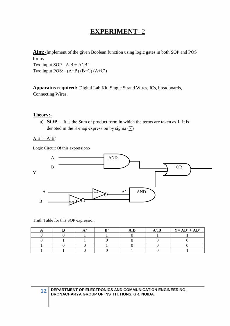
EXPERIMENT- 2
Aim:-Implement of the given Boolean function using logic gates in both SOP and POS
forms
Two input SOP - A.B + A’.B’
Two input POS: - (A+B) (B+C) (A+C’)
Apparatus required:-Digital Lab Kit, Single Strand Wires, ICs, breadboards,
Connecting Wires.
Theory:-
a) SOP: - It is the Sum of product form in which the terms are taken as 1. It is
denoted in the K-map expression by sigma (∑)
A.B. + A’B’
Logic Circuit Of this expression:-
A AND
B OR
Y
A NOT A’ AND
B NOTB’
Truth Table for this SOP expression
A B A’ B’ A.B A’.B’ Y= AB’ + AB’
0 0 1 1 0 1 1
0 1 1 0 0 0 0
1 0 0 1 0 0 0
1 1 0 0 1 0 1

13 DEPARTMENT OF ELECTRONICS AND COMMUNICATION ENGINEERING, DRONACHARYA GROUP OF INSTITUTIONS, GR. NOIDA.
AND
b) POS: - It is the product of the sums form in which the terms are taken as 0. It is
denoted in the K-Map expression by the Sign pie (π)
(A+B) (B+ C) (A + C’)
Circuit Diagram
A
B OR Y
C OR
A
CNOT
NOT OR
Truth Table foe POS expression
A B C A+B B+C A+C’ Y= (A+B)(B+C)(A+C’)
0 0 0 0 0 1 0
0 0 1 0 1 0 0
0 1 0 1 1 1 1
0 1 1 1 1 0 0
1 0 0 1 0 1 0
1 0 1 1 1 1 1
1 1 0 1 1 1 1
1 1 1 1 1 1 1
Procedure: -
For SOP form: - A.B + A’.B’
1. Place the Digital lab kit at one place.
2. Take the one AND gate ICs i.e. IC no.7408, one NOT gate IC i.e. IC no. 7404 and one OR
gate IC i.e. IC no. 7432.
3. Place these 3 ICs in the breadboard one by one.
4. Now, connect the AND gate with the inputs of A and B and other AND gate in the same
IC is given by the complement input of the A and B i.e. A’ and B’ by using NOT gate with
the help of connecting wires.
5. Give the output voltage Vcc and GROUND to all the ICs separately.
AND

14 DEPARTMENT OF ELECTRONICS AND COMMUNICATION ENGINEERING, DRONACHARYA GROUP OF INSTITUTIONS, GR. NOIDA.
6. When whole configuration is read, gently on the switch and note there output of different
values of A and B i.e. either 0 or 1.
For POS form :- (A+B)(B+C)(A+C’)
1. Place the Digital lab kit at one place.
2. Take the 1 OR, 1 AND, 1 NOT gates IC
3. Place these 3 ICs in the breadboard one by one.
4. Now, connect the OR gate of Input A or B, B or C and last one is A or C’ (i.e. complement
of C using NOT gate. Inputs are connected with the help of connecting wires.
5. When whole circuit is complete, on the switch and note down the output with different
values of A, B and C.
Result:-Hence, given Boolean Expression is implemented by the Logic Gates.
i.e. (i) A.B + A’.B’
(ii) (A+B) (B+C) (A+C’)
Precautions:-
1. Connecting wires should be rubbed with sand papers so that there is no rust.
2. Make sure that the apparatus is switched off while placing ICs and connecting of wires.
3. The connections should be tights.
4. ICs are placed in a proper way in the breadboard. There is no short of current in the in
same inputs.
Pre Experiment Questions:-
1) What is a combinational circuit?
Ans : A combinational circuit is one where the output at any time depends only on the
present combinations of inputs at that point of time.
2) What is a sequential circuit?
Ans: Sequential circuit consists of a combinational circuit to which storage elements are
Connected to form a feedback path.

15 DEPARTMENT OF ELECTRONICS AND COMMUNICATION ENGINEERING, DRONACHARYA GROUP OF INSTITUTIONS, GR. NOIDA.
3) What are the various methods of simplifying the Boolean function.
Ans: (1) Algebraic method
(2) Karnaugh method
(3) Variable entered mapping technique
(4) Quine – McCiuskey method
4) What do you mean by minterm?
Ans: Minterms are the product terms which contain all variables either in normal or
complement form.
5) What do you mean by maxterm?
Ans: Maxterms are the sum terms which contain all variables either in normal or
complement form.
Post Experiment Questions:-
1) Convert the expression Y=ACl+ AB+AC into SOP form.
Ans : Y= ACl(B+B
l ) + AB ( C+ C
l) + BC (A+A
l)
= ABCl+ AB
lC
l+ ABC + ABC
l+ABC + A
lBC
= ABCl+ AB
lC
l+ ABC + A
lBC
2) Convert the POS expression Y= (A+B) (B+C) (A+C) into canonical POS
expression.
Ans: Y= ( A+B+CCl) ( B+C+AA
l) (A+C +BB
l)
= ( A+B+C) (A+B+Cl) ( A+B+C) ( A
l+B+C) ( A+B+C) ( A+B
l+C)
= ( A+B+C) (A+B+Cl) ( A+B+C) ( A
l+B+C)
3) Define POS.
Ans: POS form expresson contains two or more OR terms which are ANDed together
to form POS expression.
4) Define SOP.

16 DEPARTMENT OF ELECTRONICS AND COMMUNICATION ENGINEERING, DRONACHARYA GROUP OF INSTITUTIONS, GR. NOIDA.
Ans: SOP form expression contains two or more AND terms which are ORed together.
5) Define canonical form representation of Boolean function.
Ans: If each term in SOP and POS form contains all the literals that are known then these
are known as canonical form.

17 DEPARTMENT OF ELECTRONICS AND COMMUNICATION ENGINEERING, DRONACHARYA GROUP OF INSTITUTIONS, GR. NOIDA.
EXPERIMENT- 3
Aim: -Verification of state tables of
1 . R-S flip-flop
2. J - K flip-flop
3. T Flip-Flop
4. D Flip-Flop
Using NAND and NOR gates.
Apparatus:- IC 7400 (NAND Gate), IC 7402 (NOR Gate), IC 7408 (AND Gate).
Theory: -In case of sequential circuits the effect of all previous inputs on the
outputs is represented by a state of the circuit. Thus, the output of the circuit at any time
depends upon its current state and the input. These also determine the next state
of the circuit. The relationship that exists among the inputs, outputs, present states
and next states can be specified by either the state table or the state diagram.
State Table: -The state table representation of a sequential circuit consists of
three sections labelledpresent state next stateand output. T he p r e sen t s t a t e
d e s i gn a t e s t h e s t a t e o f f l i p - f l op s be f o re t h e occurrence of a clock pulse.
The next state shows the states of flip -flops after the clock pulse, and the output
section lists the value of the output variables during the present state.
Flip-Flop:-The basic one bit digital memory circuit is known as flip-flop.It can store
either 0or 1. Flip-flops are classifieds according to the number of inputs.
R-S Flip-Flop:- The circuit is similar to SR latch except enable signal is replaced by
clock pulse.

18 DEPARTMENT OF ELECTRONICS AND COMMUNICATION ENGINEERING, DRONACHARYA GROUP OF INSTITUTIONS, GR. NOIDA.
Logic Diagram
Characteristic table for S-R flip flop
D Flip-Flop:-The modified clocked SR flip-flop is known as D-flip-flop.From the truth
tableof SR flip-flop we see that the output of the SR flip-flop is in unpredictable state
when the inputsare same and high. In many practical applications, these input conditions
are not required. These inputconditions can be avoided by making then complement of
each other.
Logic Diagram

19 DEPARTMENT OF ELECTRONICS AND COMMUNICATION ENGINEERING, DRONACHARYA GROUP OF INSTITUTIONS, GR. NOIDA.
Characteristic table for D flip flop
J-K Flip-Flop:- In a RS flip-flop the input R=S=1 leads to an indeterminate output. The
RSflip-flop circuit may be re-joined if both inputs are 1 than also the outputs are
complement of each other.
Logic Diagram
Characteristic table for J-K flip flop
20 DEPARTMENT OF ELECTRONICS AND COMMUNICATION ENGINEERING, DRONACHARYA GROUP OF INSTITUTIONS, GR. NOIDA.
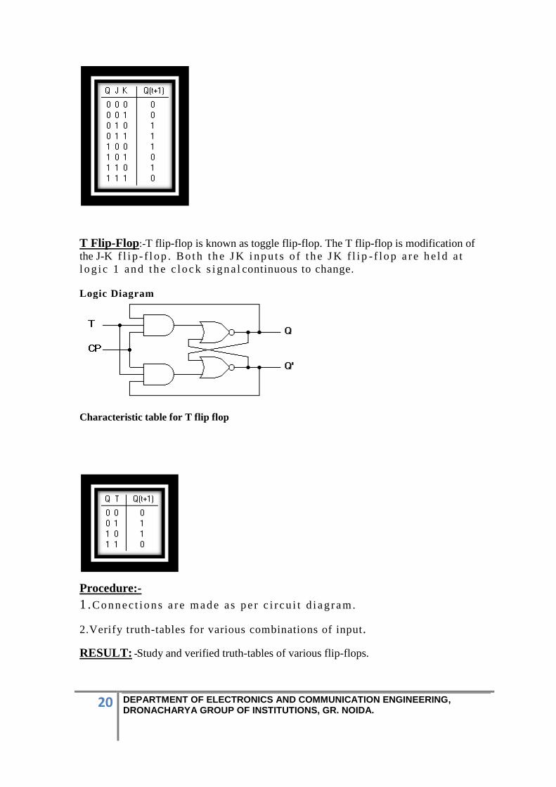
T Flip-Flop:-T flip-flop is known as toggle flip-flop. The T flip-flop is modification of
the J-K f l i p - f l op . Bo t h th e J K i np u t s o f t h e J K f l i p - f lo p a r e h e l d a t
l o g i c 1 an d th e c lock s i gn a l continuous to change.
Logic Diagram
Characteristic table for T flip flop
Procedure:-
1 .Co nn ec t io ns a r e m ad e as p e r c i rcu i t d i ag r am.
2.Verify truth-tables for various combinations of input.
RESULT: -Study and verified truth-tables of various flip-flops.

21 DEPARTMENT OF ELECTRONICS AND COMMUNICATION ENGINEERING, DRONACHARYA GROUP OF INSTITUTIONS, GR. NOIDA.
Precaution:-
1. All the IC’s should be checked before use the apparatus.
2. All LED’s should be checked.
3. All connections should be tight.
4. Always connect GROUND first and then Vcc
5. The circuit should be off before change the connections.6.After
completing the experiment switch off the supply to apparatus.
Pre Experiment Questions:-
1) What is a latch?
Ans: Storage elements that operate with signal levels are referred to as latches.
2) What is a flip flop?
Ans: Storage elements controlled by a clock transitions are called flip flop.
3) Differentiate between a latch and a flip flop.
Latch Flip flop
1) A latch checks all its inputs
continuously and changes its
outputs accordingly at any time.
1) Flip flop samples its inputs and
changes its outputs only at a time
as determined by a clocking
signal.
2) No clock is used 2) A clock is used
4) Differentiate between combinational and sequential circuits.
Combinational circuits.
Sequential circuits.
1) A circuit whose output is
dependent only on the inputs at
that instant
1) It depends on present and past
history of the inputs
2) Easy to design 2) Harder to design
3) More expensive circuit 3) Cheaper circuit
5) What happens to the JK flip flop if the J input is treated as an inverter is wired
between J and K inputs?
Ans: JK flip flop becomes D flip flop
Post Experiment Questions:-
1) How is a JK flip flop made to toggle?
Ans : If J=1 and K=1

22 DEPARTMENT OF ELECTRONICS AND COMMUNICATION ENGINEERING, DRONACHARYA GROUP OF INSTITUTIONS, GR. NOIDA.
2) When a JK flip flop isis in a no change condition?
Ans: If J=0 and K=0
3) Which is the basic sequential building block in which the output follows the data
input as long as the enable input is active?
Ans: D latch
4) Define the characteristic equation of a flip flop.
Ans: The algebraic description of the next state of the flip flop is called characteristic
equation.
5) How many stable states a flip flop has?
Ans: 2 stable states

23 DEPARTMENT OF ELECTRONICS AND COMMUNICATION ENGINEERING, DRONACHARYA GROUP OF INSTITUTIONS, GR. NOIDA.
EXPERIMENT -4
Aim: -Implementation and verification of decoder, de-multiplexer and encoder, using
logic gates.
Apparatus: -Digital trainer kit, 7432 IC, 7404 IC, 7411 IC and Connecting wires.
Theory:-
Decoder:-A decoder is a multi-inputand multi output combinational logic circuit which
converts coded input into coded outputs, where the input and output coded are different.
Logic Diagram of 2 to 4 decoder
Truth table of 2 to 4 decoder
Procedure:-
Connect the supply from the trainer kit through patch cords; also connect circuit as
per circuit diagram.

24 DEPARTMENT OF ELECTRONICS AND COMMUNICATION ENGINEERING, DRONACHARYA GROUP OF INSTITUTIONS, GR. NOIDA.
Give the input to A, B and EN trough switch.
Observe the output Y0 to Y3 on the trainer kit through LEDs.
For different combinations of inputs observe the outputs and match them with truth
table.
ENCODER:-An encoder is a combinational logic circuit .It is the reverse of a decoder
function. It has 2 to the power n input and n output lines. An encoder accepts an active
level on one of its inputs representing a digit such as a decimal /octal digit and it convert to
coded output.
Encoder is used at the starting stage to encode the message into a unique code.
Encoder encodes different types of messages into various forms. In Digital Circuits it
encodes a decimal value into a binary word. The encoded binary word has number of bits
associated with it. The number of bits depends upon the decimal value which is being
encoded. For example in case of decimal values ranging from 0 to 7 the number of bits
required to encode these values is 3.
Logic diagram of encoder

25 DEPARTMENT OF ELECTRONICS AND COMMUNICATION ENGINEERING, DRONACHARYA GROUP OF INSTITUTIONS, GR. NOIDA.
Truth trable of encoder
Procedure:-
1. Connect the supply from the trainer kit through patch chords; also connect circuit as
per circuit diagram.
2 . Givetheinputconnectionsto I0 , I1 , I2 an d I3 .
3. Observe the output Y0, Y1 on the trainer kit through LED’s
4. For different combinations of inputs observe the output and match the truth table
De- multiplexers:-.A demultiplexer sometimes abbreviated d-mux, is a circuit that has one
input and more than one output. It is used when a circuit wishes to send a signal to one of many
devices. This description sounds similar to the description given for a decoder, but a decoder is
used to select among many devices while a demultiplexer is used to send a signal among many devices.
Logic diagram of demultiplexer

26 DEPARTMENT OF ELECTRONICS AND COMMUNICATION ENGINEERING, DRONACHARYA GROUP OF INSTITUTIONS, GR. NOIDA.
Truth table of demultiplexer
Procedure:-
1. Connect the supply from the trainer kit through patch chords, also connect circuit
as per circuit diagram
2. Give input connections at I, and at selection line.
3. Observe the output D0,D1 on the trainer kit through LED’s.
4. For different combinations of inputs observe the output and match the truth table
RESULT:-Truth tables of Encoder,de-multiplexers and decoder are verified
Precautions:-
All connections should be made neat and tight.
Digital lab kits and ICs should be handled with utmost care.
While making connections main voltage should be kept switched off.
Never touch live and naked wires.
Pre Experiment Questions:-
1) What is a decoder?
Ans: A decoder is a combinational circuit which has n inputs and to a maximum of 2n
outputs.
2) What is a demultiplexer?
Ans: Demultoplexer is a combinational logic circuit which accepts one input and
distributes it over several outputs.

27 DEPARTMENT OF ELECTRONICS AND COMMUNICATION ENGINEERING, DRONACHARYA GROUP OF INSTITUTIONS, GR. NOIDA.
3) Differentiate between decoder and demultiplexer.
Ans: A decoder is a combinational circuit which has n inputs and to a maximum of 2n
outputs. A decoder with enable input is known as demultiplexer.
4) What is an encoder?
Ans: An encoder is a combinational circuit which has 2n
input lines and n output lines.
5) What is priority encoder?
Ans: In priority encoder if two or more inputs are equal to 1 at the same time, the input
having the highest priority will take precedence.
Post Experiment Questions:-
1) Which digital system translates coded characters into a more useful form?
Ans: Decoder
2) Why is a demultiplexer called data distributor?
Ans: Because the input will be distributed to one of the outputs.
3) Give the applications of decoder.
Ans: Decoders are used for data distribution, code conversion and they are used to route
the input data to a specified output line.
4) How many control inputs are there in 1:16 demultiplexer?
Ans: 4

28 DEPARTMENT OF ELECTRONICS AND COMMUNICATION ENGINEERING, DRONACHARYA GROUP OF INSTITUTIONS, GR. NOIDA.
EXPERIMENT-5
Aim:-Implementation of 4x1 multiplexer, using logic gates.
Apparatus: -Digital trainer kit, AND-7411, OR-7432, NOT-7404 Gate IC, Connecting
wires.
Theory:-
MULTIPLEXER: -A multiplexer (MUX) is a device that accepts data from one of
many inputsources for transmission over a common shared line. To achieve this
MUX has severaldata lines and a single output along with data-select inputs, which
permit digital data onany of the inputs to be switched to the output line. The
logic symbol for a 1 to 4 dataselector/multiplexer is shown in Figure
Block diagram of multiplexer
The selection lines decide the number of inputs lines of particular multiplexer.
If the number of n inputs lines is equal to 2m, then m select lines are required
to select one of the n input line.
Note that if a binary zero appears on the data-select lines then data on input line D0
willappear on the output. Thus, data output Y is equal to D0 if and only if S1=0 and S0=0.
Y=D0.S1’.S0’Similarly, the data output is equal to D1, D2 and D3 for y=C1.S1’.S0’
,Y=C2.S0’. S1 and Y=C3.S0.S1 respectively. Thus the total multiplexer logic expression,
formed from ORing terms i
The implementation of this equation is as shown in figure:

29 DEPARTMENT OF ELECTRONICS AND COMMUNICATION ENGINEERING, DRONACHARYA GROUP OF INSTITUTIONS, GR. NOIDA.
Logic diagram of multiplexer
Truth table of mux
DATA SELECT INPUT INPUT
SELECTED S1 S0
0 0 D0
0 1 D1
1 0 D2
1 1 D3

30 DEPARTMENT OF ELECTRONICS AND COMMUNICATION ENGINEERING, DRONACHARYA GROUP OF INSTITUTIONS, GR. NOIDA.
PROCEDURE:-
1 . Connections are made as per circuit diagram.
2. Verify the truth table.
3. Also connect Vcc and Ground then performed experiment.
Result:-Study of 4×1 multiplexer and verified its truth table.
Precautions:-
1. All ICs should be checked before starting the experiment.
2. All the connection should be tight.
3. Always connect ground first and then connect Vcc.
4. Suitable type wire should be used for different types of circuit.
5. The kit should be off before change the connections.
6. After completed the experiments switch off the supply of the apparatus
Pre Experiment Questions:-
1) What is a multiplexer?
Ans: A multiplexer accepts two or more streams of data and combines them into one
stream.
2) How many select lines will a 16 to 1 multiplexer will have?
Ans: 4
3) What is the function of enable input on a multiplexer chip?
Ans: To activate the entire chip.
Post Experiment Questions:-
1) Why multiplexer is called as data selector?
Ans: Because multiplexer selects one of several input signals and directs to the output.
2) Give the applications of multiplexer.
Ans: Multiplexers are used in data routing, data selection, parallel to serial conversion
and waveform generation.

31 DEPARTMENT OF ELECTRONICS AND COMMUNICATION ENGINEERING, DRONACHARYA GROUP OF INSTITUTIONS, GR. NOIDA.
3) How many control inputs are there in 16 to 1 demultiplexer?
Ans: 4
4) How many select lines will a 32:1 multiplexer will have?
Ans: For 32 inputs, 5 select lines will be required, as 25= 32.

32 DEPARTMENT OF ELECTRONICS AND COMMUNICATION ENGINEERING, DRONACHARYA GROUP OF INSTITUTIONS, GR. NOIDA.
EXPERIMENT-6
Aim: -Implementation of 4-bit parallel adder, using 7483 IC.
Apparatus:-
1. Digital Trainer Kit.
2. IC 7483
3. Connecting Wires
Theory:-
Adder: -An adder is a logic circuit which adds two or three bits at a time and give sum and
carry as the result.
Parallel Adder:-
A n-bit parallel adder can be constructed using number of full adders circuit connected in
parallel the carry output of each is connected to the carry input of the next higher-order
adder. Since all the bits of the augends and addend are fed into the adder circuits
simultaneously and the additions in each position are known as parallel adder.
A3 A2 A1 A0 → Augends bits
B3 B2 B1 B0 → Addend bits
S3 S2 S1 S0 → Sum bits
LOGIC DIAGRAM OF BCD ADDER
Pin diagram of IC 7483

33 DEPARTMENT OF ELECTRONICS AND COMMUNICATION ENGINEERING, DRONACHARYA GROUP OF INSTITUTIONS, GR. NOIDA.
Procedure:-
1 .Connect ground and Vcc to 7483 IC from trainer kit through patch cords.
2. Connect inputs A0, A1, A2, A3 and B0, B1, B2, B3 to logic input switches.
3. Connect carry in from pin no.13 to ground so that carry input (CY1) will be logic
‘0’state.
4. Connect S0, S1, S2, S3 and carry out (CY0) from pin nos. 9, 6, 2, 15 and 14 to the
outputdisplay.5.Verify truth tables for different combinations of inputs.
TRUTH TABLE:- The Truth table operation of the 4-bit Parallel Adder is shown below:
INPUTS
OUTPUTS
A0 A1 A2 A3 B0 B1 B2 B3 CY1 S0 S1 S2 S3 CY0
0 0 0 1 0 1 0 1 1 1 1 0 0 1
1 0 0 0 1 1 1 0 0 0 0 0 0 1
Result:-
For various combinations of selected input lines, observed the LED output and verified the
truth table.

34 DEPARTMENT OF ELECTRONICS AND COMMUNICATION ENGINEERING, DRONACHARYA GROUP OF INSTITUTIONS, GR. NOIDA.
Precautions:-
1. All ICs should be checked before starting the experiment.
2. All the connection should be tight.
3. Always connect ground first and then connect Vcc.
4. Suitable type wire should be used for different types of circuit.
5. The kit should be off before change the connections.
6. After completed the experiments switch off the supply of the apparatus.
Pre Experiment Questions:-
1) What is half adder?
Ans: A logic circuit which performs the operation of two binary bits is called a half
adder.
2) Write the truth table for half adder.
Ans:
Inputs Outputs
A B S C
0 0 0 0
0 1 1 0
1 0 1 0
1 1 0 1
3) What is full adder?
Ans: A full adder is a combinational logic circuit that performs the arithmetic sum of
three input bits.
4) What is parallel adder?
Ans: Parallel adders are digital circuits that compute the addition of variable binary strings
of equivalent or different size in parallel.
5) Write the truth table for full adder.
Ans:
A B C S Co
0 0 0 0 0
0 0 1 1 0
0 1 0 1 0
0 1 1 0 1
1 0 0 1 0

35 DEPARTMENT OF ELECTRONICS AND COMMUNICATION ENGINEERING, DRONACHARYA GROUP OF INSTITUTIONS, GR. NOIDA.
1 0 1 0 1
1 1 0 0 1
1 1 1 1 1
Post Experiment Questions:-
1) Draw the block diagram of full adder as a combination of two half adder.
Ans:
2) Write the Boolean expression for the outputs S and Co of a full adder from the
truth table.
Ans: S = C ( A B )
Co = AB + C( A B )
3) What is the difference between adder and parallel adder?
Ans: serial adder adds bits serially but parallel adder add bits at the same time.
Serial adder depends on previous outputs but parallel adder does not depends on
previous outputs. Parallel adder takes less time to execute compare to serial adder.
4) How many full adders are required to construct an m-bit parallel adder?
Ans: m full adder

36 DEPARTMENT OF ELECTRONICS AND COMMUNICATION ENGINEERING, DRONACHARYA GROUP OF INSTITUTIONS, GR. NOIDA.
EXPERIMENT-7 Aim:- Design, and verify the 4-bit synchronous counter.
Apparatus:-
S.No. COMPONENT SPECIFICATION QTY.
1. JK FLIP FLOP IC 7476 2
2. 4 I/P AND GATE IC 7411 1
3. OR GATE IC 7432 1
4. XOR GATE IC 7486 1
5. NOT GATE IC 7404 1
6. IC TRAINER KIT - 1
7. PATCH CORDS - 35
Theory:-
Synchronous counter: -A simple way of implementing the logic for each bit of an
ascending counter (which is what is depicted in the image to the right) is for each bit to
toggle when all of the less significant bits are at a logic high state. For example, bit 1
toggles when bit 0 is logic high; bit 2 toggles when both bit 1 and bit 0 are logic high; bit 3
toggles when bit 2, bit 1 and bit 0 are all high; and so on.
Synchronous counters can also be implemented with hardware finite state machines.Which
are more complex but allow for smoother, more stable transitions?
Hardware-based counters are of this type and they can be implemented using the IC 7476
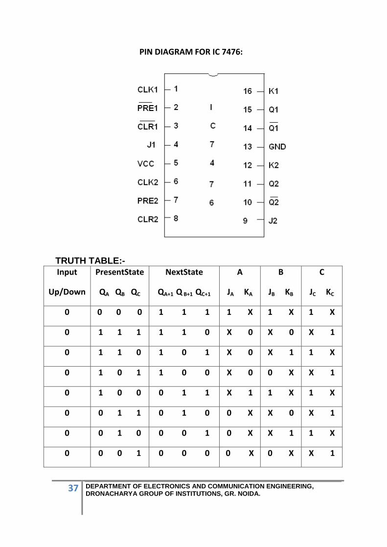
37 DEPARTMENT OF ELECTRONICS AND COMMUNICATION ENGINEERING, DRONACHARYA GROUP OF INSTITUTIONS, GR. NOIDA.
PIN DIAGRAM FOR IC 7476:
TRUTH TABLE:-
Input
Up/Down
PresentState
QA QB QC
NextState
QA+1 Q B+1 QC+1
A
JA KA
B
JB KB
C
JC KC
0 0 0 0 1 1 1 1 X 1 X 1 X
0 1 1 1 1 1 0 X 0 X 0 X 1
0 1 1 0 1 0 1 X 0 X 1 1 X
0 1 0 1 1 0 0 X 0 0 X X 1
0 1 0 0 0 1 1 X 1 1 X 1 X
0 0 1 1 0 1 0 0 X X 0 X 1
0 0 1 0 0 0 1 0 X X 1 1 X
0 0 0 1 0 0 0 0 X 0 X X 1

38 DEPARTMENT OF ELECTRONICS AND COMMUNICATION ENGINEERING, DRONACHARYA GROUP OF INSTITUTIONS, GR. NOIDA.
1 0 0 0 0 0 1 0 X 0 X 1 X
1 0 0 1 0 1 0 0 X 1 X X 1
1 0 1 0 0 1 1 0 X X 0 1 X
1 0 1 1 1 0 0 1 X X 1 X 1
1 1 0 0 1 0 1 X 0 0 X 1 X
1 1 0 1 1 1 0 X 0 1 X X 1
1 1 1 0 1 1 1 X 0 X 0 1 X
1 1 1 1 0 0 0 X 1 X 1 X 1
TRUTH TABLE OF 4 BIT SYNCHRONOUS COUNTERS
LOGIC DIAGRAM

39 DEPARTMENT OF ELECTRONICS AND COMMUNICATION ENGINEERING, DRONACHARYA GROUP OF INSTITUTIONS, GR. NOIDA.
State diagram
Procedure:-
(i) Connections are given as per circuit diagram.
(ii) Logical inputs are given as per circuit diagram.
(iii) Observe the output and verify the truth table.
Result: -Study of 4 bit synchronous counters and verified its truth table.
Precautions:-
1. All ICs should be checked before starting the experiment.
2. All the connection should be tight.
3. Always connect ground first and then connect Vcc.
4. Suitable type wire should be used for different types of circuit.
5. The kit should be off before change the connections.
6. After completed the experiments switch off the supply of the apparatus

40 DEPARTMENT OF ELECTRONICS AND COMMUNICATION ENGINEERING, DRONACHARYA GROUP OF INSTITUTIONS, GR. NOIDA.
Pre Experiment Questions:-
1) What is a register?
Ans: A register is basically a set of flip flops logically connected to perform
various operations.
2) What is the need of a register?
Ans Registers are used for temporary storage of binary information. Registers are
also used for shifting the binary information stored in it.
3) What is a counter?
Ans: A counter is a sequential logic circuit capable of counting the number of clock
pulses arriving at its clock input.
4) What is a synchronous counter?
Ans: Synchronous counter is one in which all the flip flops are triggered
simultaneously by clock pulse.
5) How the synchronous counter eliminate the delay problems encountered with
asynchronous counters.
Ans: :In synchronous counters all the flip flops are triggered simultaneously by
clock pulse. This eliminates the delay problem.
Post Experiment Questions:-
1) How many flip flops are required to construct a decade counter?
Ans: 4
2) How many different states a 3 bit synchronous counter have?
Ans: 8
3) For how many clock pulses the final output of a modulus 8 counter occur?
Ans: 8 clock pulses
4) A 4 bit up/down binary counter is in the down mode and in the 1100 state. To
what state does the counter go on the next clock pulse.
Ans: 1011

41 DEPARTMENT OF ELECTRONICS AND COMMUNICATION ENGINEERING, DRONACHARYA GROUP OF INSTITUTIONS, GR. NOIDA.
EXPERIMENT-8
AIM: - To design and verify 4 bit ripple (asynchronous counter).
APPARATUS REQUIRED:-
S.No. COMPONENT SPECIFICATION QTY.
1. JK FLIP FLOP IC 7476 2
2. NAND GATE IC 7400 1
3. IC TRAINER KIT - 1
4. PATCH CORDS - 30
THEORY:-
A counter is a register capable of counting number of clock pulse arriving at its clock
input. Counter represents the number of clock pulses arrived. A specified sequence of
states appears as counter output. This is the main difference between a register and a
counter. There are two types of counter, synchronous and asynchronous. In synchronous
common clock is given to all flip flop and in asynchronous first flip flop is clocked by
external pulse and then each successive flip flop is clocked by Q or Q output of previous
stage. A soon the clock of second stage is triggered by output of first stage. Because of
inherent propagation delay time all flip flops are not activated at same time which results
in asynchronous operation.

42 DEPARTMENT OF ELECTRONICS AND COMMUNICATION ENGINEERING, DRONACHARYA GROUP OF INSTITUTIONS, GR. NOIDA.
PIN DIAGRAM FOR IC 7476:
LOGIC DIAGRAM FOR 4 BIT RIPPLE COUNTER:

43 DEPARTMENT OF ELECTRONICS AND COMMUNICATION ENGINEERING, DRONACHARYA GROUP OF INSTITUTIONS, GR. NOIDA.
TRUTH TABLE:-
CLK QA QB QC QD
0 0 0 0 0
1 1 0 0 0
2 0 1 0 0
3 1 1 0 0
4 0 0 1 0
5 1 0 1 0
6 0 1 1 0
7 1 1 1 0
8 0 0 0 1
9 1 0 0 1
10 0 1 0 1
11 1 1 0 1
12 0 0 1 1
13 1 0 1 1
14 0 1 1 1
15 1 1 1 1

44 DEPARTMENT OF ELECTRONICS AND COMMUNICATION ENGINEERING, DRONACHARYA GROUP OF INSTITUTIONS, GR. NOIDA.
Procedure:-
(i) Connections are given as per circuit diagram.
(ii) Logical inputs are given as per circuit diagram.
(iii) Observe the output and verify the truth table.
Result: -
Study of 4 bit synchronous counter and verified its truth table
Precautions:-
1. All ICs should be checked before starting the experiment.
2. All the connection should be tight.
3. Always connect ground first and then connect Vcc.
4. Suitable type wire should be used for different types of circuit.
5. The kit should be off before change the connections.
6. After completed the experiments switch off the supply of the apparatus
Pre Experiment Questions:-
1) What is an asynchronous counter?
Ans: Asynchronous counter is one in which flip flops are connected in such a way
that the first flip flop output is the clock for the nest flip flop.
2) What is the major drawback of asynchronous counters?
Ans: High frequency applications are limited because of internal propagation delay.
3) What is modulus counter?
Ans: The number of states through which the counter passes before returning to the
starting state is called modulus counter.
4) What is a state diagram?
Ans: A state diagram is a graphical representation represented by circles and the
transition between states is indicated by directed lines connecting the circles.

45 DEPARTMENT OF ELECTRONICS AND COMMUNICATION ENGINEERING, DRONACHARYA GROUP OF INSTITUTIONS, GR. NOIDA.
5) What is state table?
Ans: The state table represents the state diagram in tabular form. It consists of
present state, next state and flip flop inputs.
Post ExperimentQuestions:-
1) What factor determines whether a counter will operate as a count up or count
down counter?
Ans: When the signal is high, the counter operates as an up counter, when the
signal is low the counter operates as a down counter.
2) How many different states 2 bit asynchronous counters have?
Ans: 4
3) Differentiate between synchronous and asynchronous counters.
Asynchronous counter Synchronous counter
1) All flip flops are not clocked
simultaneously
1) All flip flops are clocked
simultaneously
2) Design is very simple eve for
more number of states
2) Complex logic circuits as the
number of states increases.
3) Low speed 3) Higher speed as compared to
asynchronous counters
4) How the up counter can be made to work as a down counter?
Ans: By taking the counter outputs Qlinstead of Q the up counter can be made to
work as a down counter.