logic design ii (17.342) spring 2012 lecture...
TRANSCRIPT

1
Logic Design II (17.342)
Spring 2012
Lecture Outline
Class # 01
January 26, 2012
Dohn Bowden

2
Today’s Lecture
• Administrative
• General Course Overview
• Main Lecture Topic
• Lab
• Homework

3
CourseAdmin

4
Administrative
• Admin for tonight …
– Attendance/Introductions/Backgrounds
– Syllabus
– Textbook
– 17.342 Web Site
– Email List creation
– Course Objectives

5
Attendance/Introductions/Backgrounds
• Attendance …
– When called … please introduce yourself
• Include the following
– When did you take Logic Design I
– Education
– Work Experience
– Other notable work/engineering/hobbies
– Future Plans

6
My Background
• Education
• Work Experience
• Other notable work/engineering/hobbies
• Future Plans

7
Syllabus
• Syllabus
– Hard copies available
– Electronic copy available on the class website
• Web Address will be provided in an upcoming slide
8
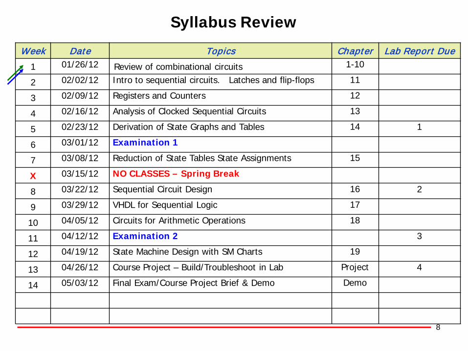
Syllabus Review
Week Date Topics Chapter Lab Report Due
1 01/26/12 Review of combinational circuits 1-10
2 02/02/12 Intro to sequential circuits. Latches and flip-flops 11
3 02/09/12 Registers and Counters 12
4 02/16/12 Analysis of Clocked Sequential Circuits 13
5 02/23/12 Derivation of State Graphs and Tables 14 1
6 03/01/12 Examination 1
7 03/08/12 Reduction of State Tables State Assignments 15
X 03/15/12 NO CLASSES – Spring Break
8 03/22/12 Sequential Circuit Design 16 2
9 03/29/12 VHDL for Sequential Logic 17
10 04/05/12 Circuits for Arithmetic Operations 18
11 04/12/12 Examination 2 3
12 04/19/12 State Machine Design with SM Charts 19
13 04/26/12 Course Project – Build/Troubleshoot in Lab Project 4
14 05/03/12 Final Exam/Course Project Brief & Demo Demo

9
Grading Policy
• Grading Policy is also located at the bottom of syllabus
• Exam # 1 (20%) Exam #2 (20%)
• Laboratory … including lab reports (30%)
• Final Exam/Course Project (30%)
A 93-100 A- 90-92 B+ 87-89 B 83-86 B- 80-82C+ 77-79 C 73-76 C- 70-72D+ 67-69 D 60-66F Below 60

10
Class Hours
• Thursday evenings … 6:30 – 9:30 PM in PA-411 (Pasteur)• See syllabus for schedule of classes
• Call/email if you will not be in class …
• I am available for extra help Before /After class • If possible … please schedule in advance so I will ensure that
I am available
11
Textbooks
• Roth & Kinney, “Fundamentals of Logic Design, 6th ED, CengageLearning, 2010

12
Software (Optional)
• If you want to purchase the software …
– Capilano Computing Systems Ltd., “LogicWorks 5: Interactive Circuit Design Software”, Addison Wesley, 2004
… OR …
– Capilano Computing Systems Ltd., “LogicWorks 4: Interactive Circuit Design Software”, Addison Wesley, 1999
• Otherwise either LogicWorks 4 or 5 is available in the computer laboratory (BL - 420) … OR … Engineering Laboratory (EB - 321)

13
Course Web Site
• The Course Homepage is at:
http://faculty.uml.edu/dbowden
• This website will contain the following:
• Syllabus • Lab material
– Labs procedures– Datasheets
• Reference documents– Such as the textbook material– Links
• Additional class material • Homework

14
Email Distribution List
• I will be creating a class email list
• Email me at:
• This will ensure that your correct email address or addresses are included
• The email list will allow me to provide information to each of you

15
Course Objectives
• What do you want to get out of this class?
• My goals for the course …

16
Questions?

17
General Course Overview

18
General Course Overview
• Typical Lecture/Class Structure
– Administrative
– Main Lecture Topic(s)
– Lab Discussion
– Homework

19
General Overview
• This is a lecture orientated course WITH associated lab work …
– Labs are mainly problem solving utilizing interactive circuit design software
• Software is …
– LogicWorks 5 … OR …
– LogicWorks 4

20
General Overview
• Homework
– Homework exercises will not be collected/graded
– Homework exercises will not be counted towards the course grade
– It is important that you practice these exercises in order to understand the course materials.
• Solutions (or answers for simpler problems) to the homework exercises will be provided so that you can verify your work

21
General Course Overview

22
Review of
Logic Design I
(17.341)

23
Logic Design I (17.341)
• Overview/review of Logic Design I (17.341) material
– Basic high level overview …
• What was learned?
• How did we use it?
– We will then go into some details of Logic Design I material
• IMPORTANT - Logic Design I is the foundation for Logic Design II
– Suggest each of you review Chapters 1 – 10 of the text
24
Logic Design I (17.341) – con’t
• Logic Design I topics are NOT independent of each other … it’s the foundation for the material in Logic Design II!
• They ALL inter-relate to one another
• The goals tonight are …
– To see how they relate to one another … AND …
– How do we use them
• If needed … I shall expand on topics that may be cause for confusion … HOWEVER … you should review areas that you are weak in

25
Logic Design I (17.341) – con’t
• First we introduced the basic digital systems …
• We then reviewed Numbers and Codes …
– Which is the Foundation for our course material
• Boolean Algebra was discussed in detail …
– Basic logical operations– Basic laws– Standard forms for expressions– Theorems
26
Logic Design I (17.341) – con’t
• Then we looked at the relationship between Boolean functions and digital circuits
– Functions were translated into circuits … and …– We analyzed circuit diagrams to determine the function of a
given circuit
• Karnaugh Maps (K-Maps)
– Like Boolean algebra, K-Maps are a simplification tool applicable to digital logic
– Graphical method for Boolean functions
27
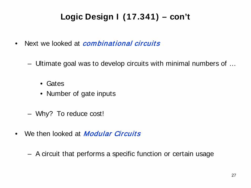
Logic Design I (17.341) – con’t
• Next we looked at combinational circuits
– Ultimate goal was to develop circuits with minimal numbers of …
• Gates• Number of gate inputs
– Why? To reduce cost!
• We then looked at Modular Circuits
– A circuit that performs a specific function or certain usage
28
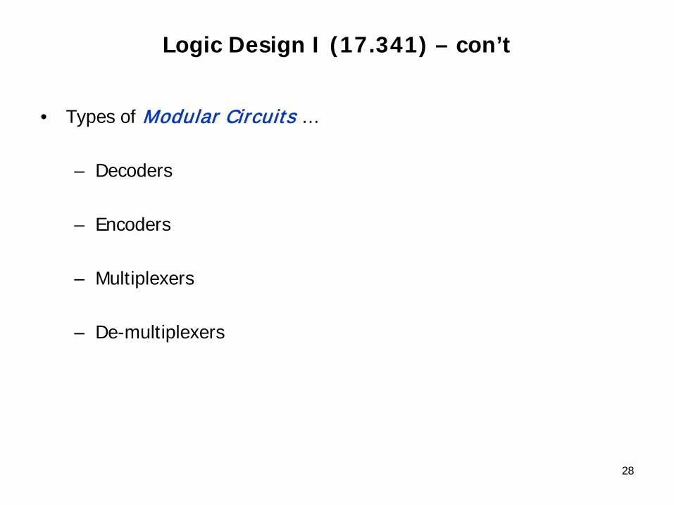
Logic Design I (17.341) – con’t
• Types of Modular Circuits …
– Decoders
– Encoders
– Multiplexers
– De-multiplexers
29
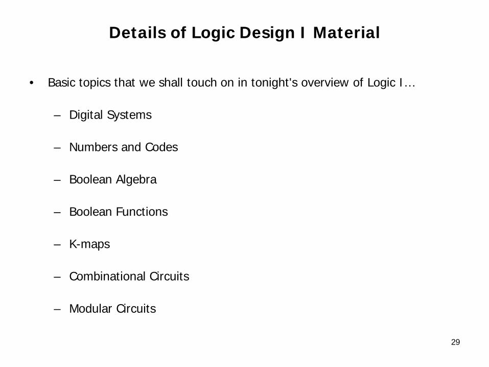
Details of Logic Design I Material
• Basic topics that we shall touch on in tonight's overview of Logic I…
– Digital Systems
– Numbers and Codes
– Boolean Algebra
– Boolean Functions
– K-maps
– Combinational Circuits
– Modular Circuits

30
Chapter 1 …
Introduction and
Number Systems/Conversions

31
Introduction to Digital Systems …
32
Introduction to Digital Systems
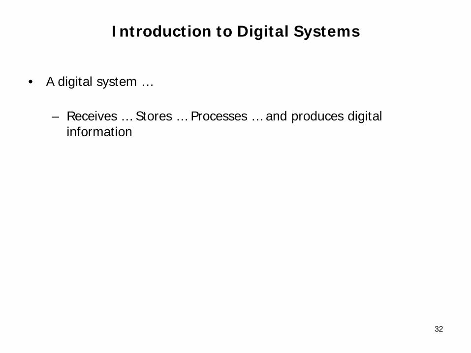
• A digital system …
– Receives … Stores … Processes … and produces digital information

33
Introduction to Digital Systems
• Takes a set of discrete information inputs and discrete internal information (system state) and generates a set of discrete information outputs.
System State
DiscreteInformationProcessingSystem
DiscreteInputs Discrete
Outputs
34
Introduction to Digital Systems
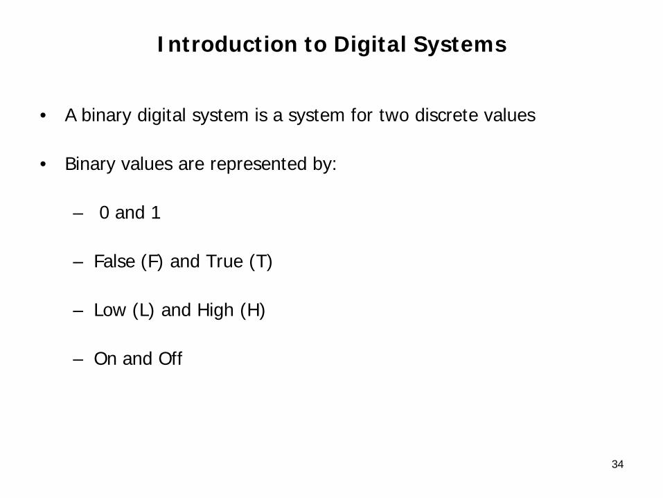
• A binary digital system is a system for two discrete values
• Binary values are represented by:
– 0 and 1
– False (F) and True (T)
– Low (L) and High (H)
– On and Off
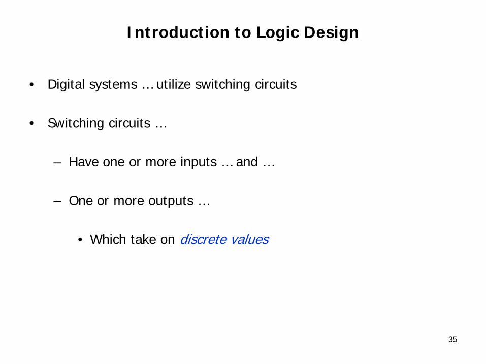
Introduction to Logic Design
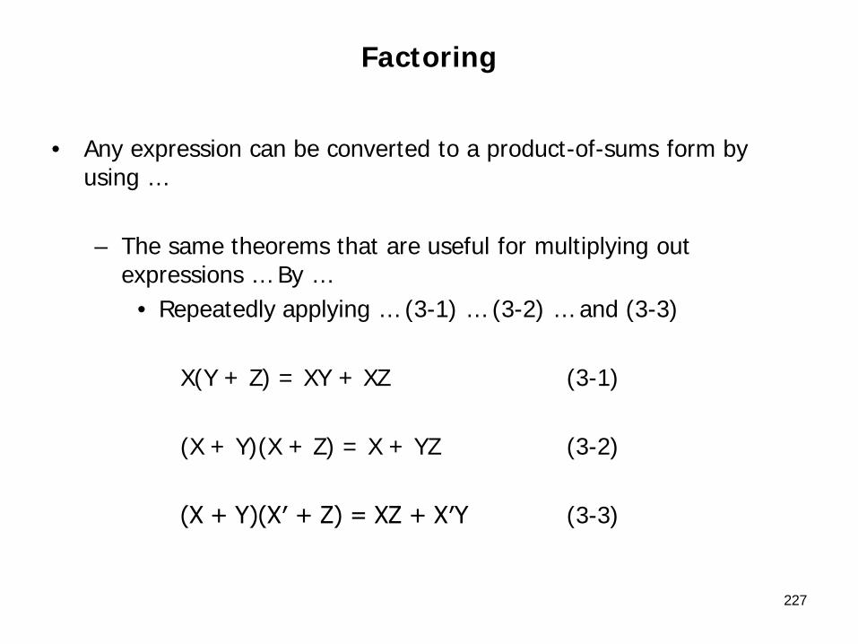
• Digital systems … utilize switching circuits
• Switching circuits …
– Have one or more inputs … and …
– One or more outputs …
• Which take on discrete values
35

Introduction to Logic Design
36

Introduction to Logic Design
• Logic circuits have …
– A specified relationship between signals at the input terminals of the circuit … and …
– Signals at the output terminals of the circuit
37
Introduction to Logic Design
• We applied switching theory …to …
– The solution of logic design problems
• We learned both …
– The basic theory of switching circuits … and …
– How to apply it
38
39
Introduction to Digital Systems
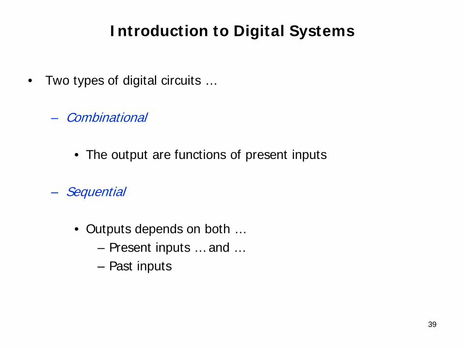
• Two types of digital circuits …
– Combinational
• The output are functions of present inputs
– Sequential
• Outputs depends on both …– Present inputs … and …– Past inputs
40
Number Systems …
Binary Numbers
• We use binary numbers …
– Because the outputs of most switching devices assume only two different values
• Binary numbers and number systems were discussed …
– Overview is as follows …
41

42
Positional Notation
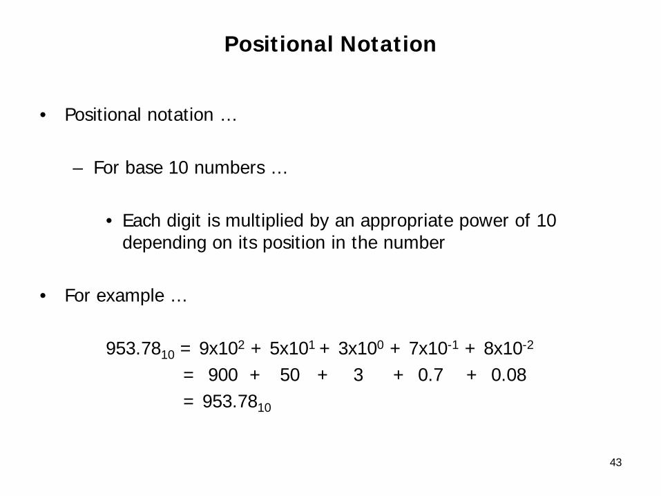
Positional Notation
• Positional notation …
– For base 10 numbers …
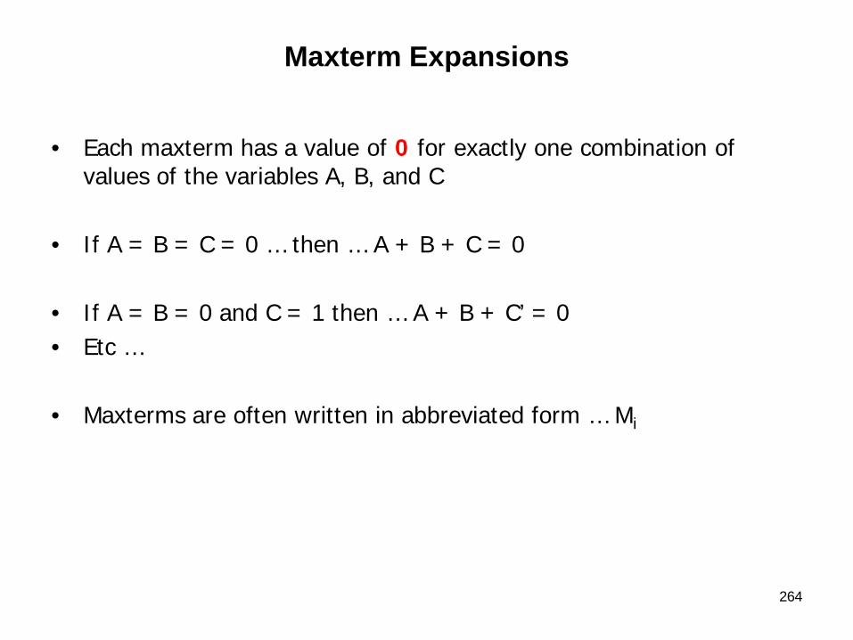
• Each digit is multiplied by an appropriate power of 10 depending on its position in the number
• For example …
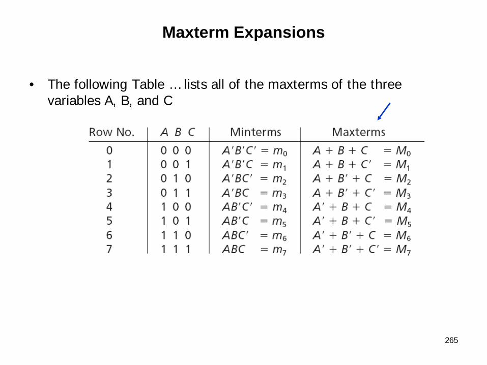
953.7810 = 9x10² + 5x101 + 3x100 + 7x10⁻¹ + 8x10-2
= 900 + 50 + 3 + 0.7 + 0.08= 953.7810
43

Positional/Polynomial Representations
44
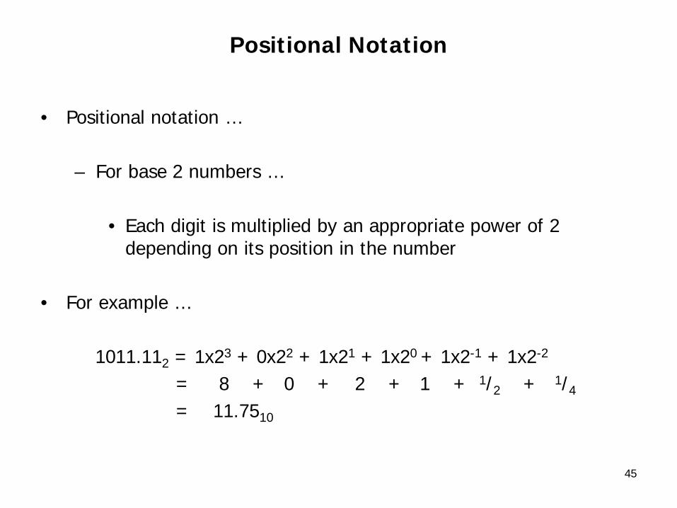
Positional Notation
• Positional notation …
– For base 2 numbers …
• Each digit is multiplied by an appropriate power of 2 depending on its position in the number
• For example …
1011.112 = 1x23 + 0x22 + 1x21 + 1x20 + 1x2-1 + 1x2-2
= 8 + 0 + 2 + 1 + 1/2 + 1/4
= 11.7510
45

Positional Notation
• The decimal and binary points separates the …
– Positive and negative powers
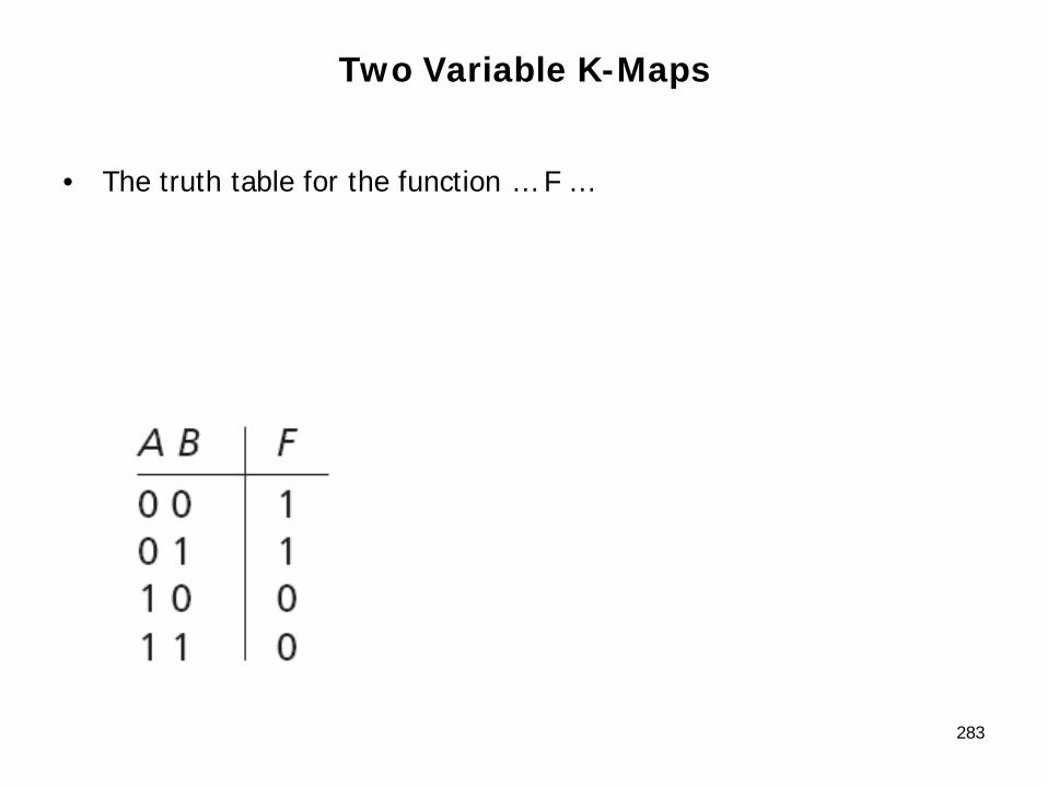
953.7810 = 9x10² + 5x101 + 3x100 + 7x10⁻¹ + 8x10⁻²
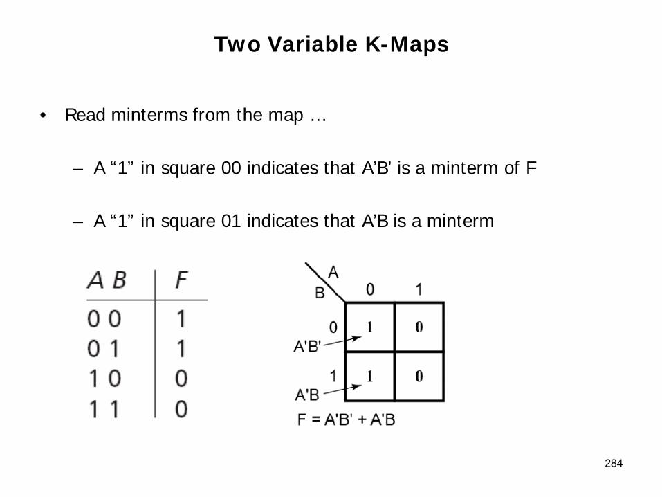
1011.112 = 1x23 + 0x22 + 1x21 + 1x20 + 1x2-1 + 1x2-2
46

Positional Notation
• The base of a number system … such as …
– Base 10
953.7810
– … or …
– Base 2
1011.112
• Is also called the Radix47

48
Numbers …
• The base or radix of a number system is …
– The total number of digits for that system
SYSTEM Radix (base)• Binary 2• Octal 8• Decimal 10• Hexadecimal 16
Fundamentals of Logic DesignCh 2, page 5
Logic and Computer Design FundamentalsCh 1, page 13
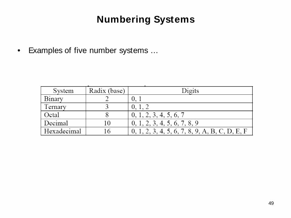
Numbering Systems
• Examples of five number systems …
49
Numbering Systems
• Conversions were discussed …
50

51
Power Series Expansion
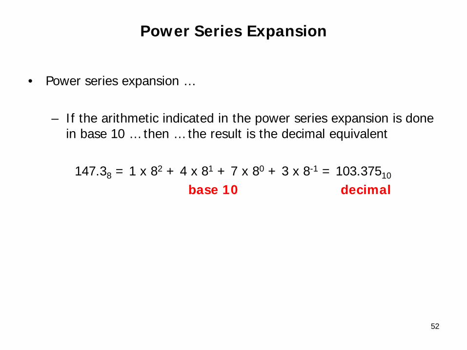
Power Series Expansion
• Power series expansion …
– If the arithmetic indicated in the power series expansion is done in base 10 … then … the result is the decimal equivalent
147.38 = 1 x 82 + 4 x 81 + 7 x 80 + 3 x 8-1 = 103.37510
base 10 decimal
52

Power Series Expansion
• The power series expansion can be used to convert to any base …
– Converting 14710 to base 3 would be written as …
14710 = 1 x (101)2 + (11) x (101)1 + (21) x (101)0
base 3
» Where all the numbers on the right hand side are base 3 numbers … MUST USE base 3 arithmetic
– Then … the result is base 3 equivalent
• However … this is not very convenient if the arithmetic is being done by hand
53
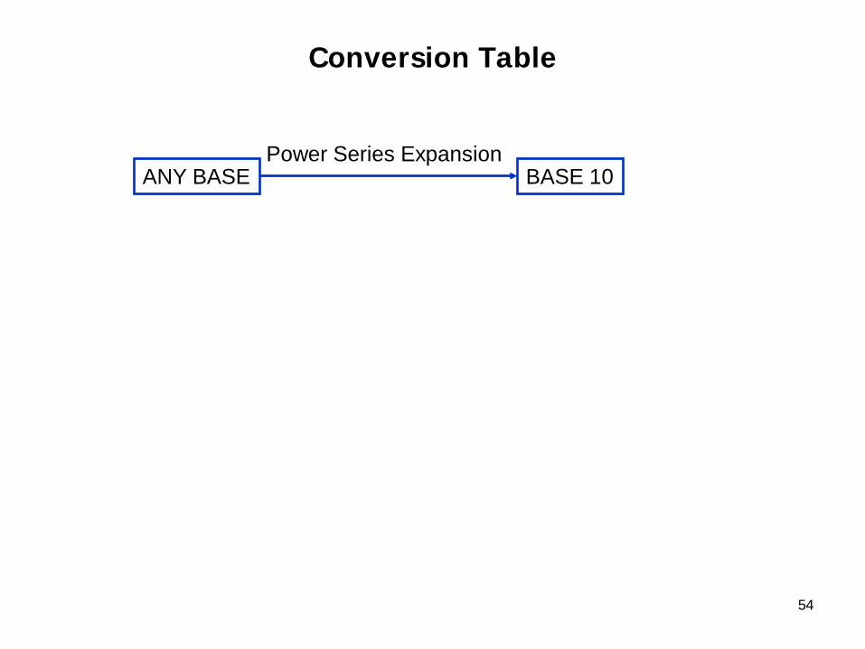
Conversion Table
54
ANY BASE BASE 10Power Series Expansion
55
Division Method

Division Method
• Division Method …
– The conversion of a decimal integer N to base R
N = (a0a1a2….an)R
56
Division Method
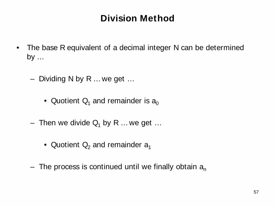
• The base R equivalent of a decimal integer N can be determined by ...
– Dividing N by R … we get …
• Quotient Q1 and remainder is a0
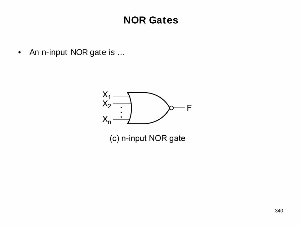
– Then we divide Q1 by R … we get …
• Quotient Q2 and remainder a1
– The process is continued until we finally obtain an
57
Division Method
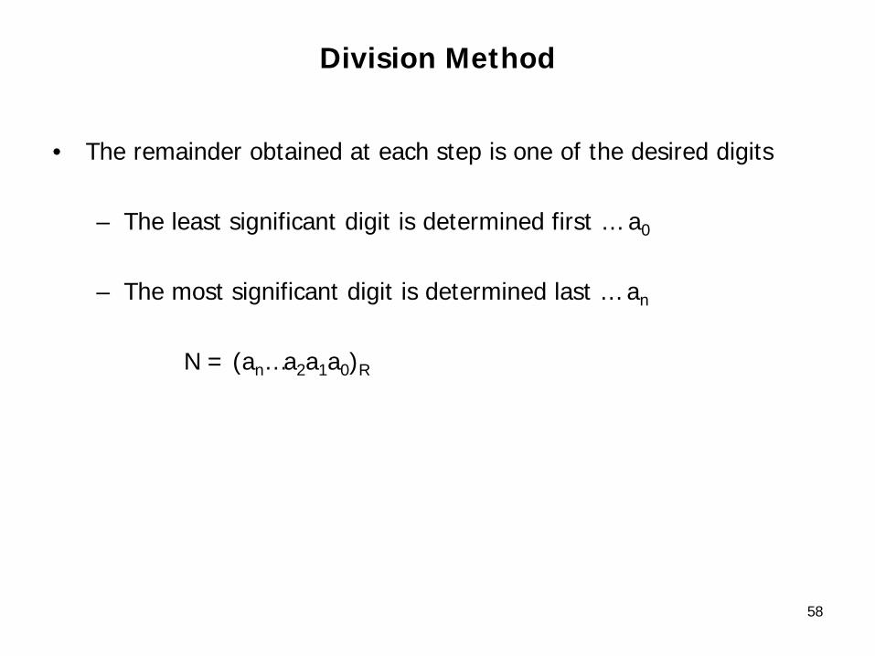
• The remainder obtained at each step is one of the desired digits
– The least significant digit is determined first … a0
– The most significant digit is determined last … an
N = (an…a2a1a0)R
58
Division Method
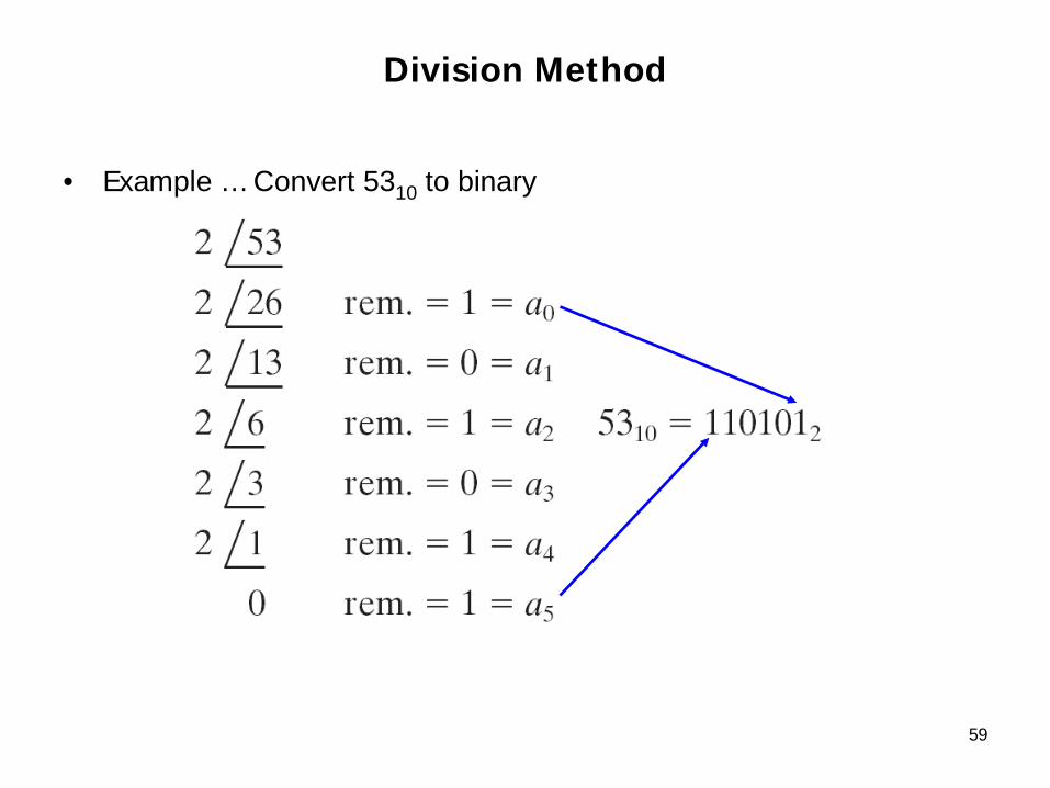
• Example … Convert 5310 to binary
59

Conversion Table
60
ANY BASE BASE 10Power Series Expansion
Division Method
61
Successive Multiplications

Successive Multiplications
• Successive Multiplications …
– Conversion of a decimal fraction F to base R
• Accomplished by using successive multiplications by R
• The integer part obtained at each step is one of the desired digits
• The most significant digit is obtained first
62

Successive Multiplications
• EXAMPLE … Convert 0.62510 to binary
63
Successive Multiplications
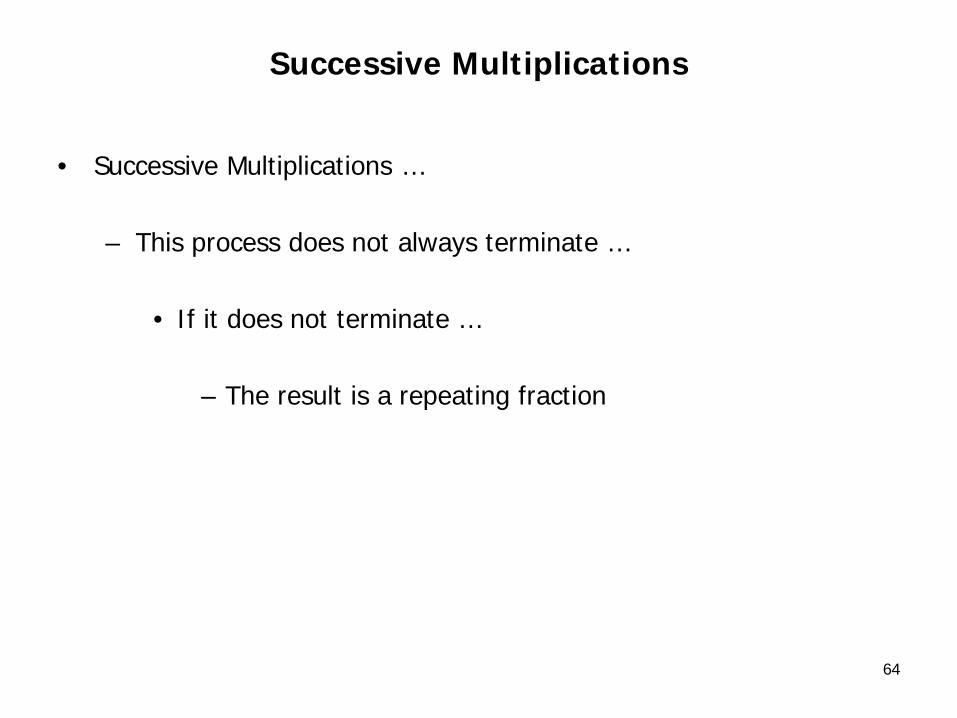
• Successive Multiplications …
– This process does not always terminate …
• If it does not terminate …
– The result is a repeating fraction
64

Successive Multiplications
• EXAMPLE … Convert 0.710 to binary
65

Conversion Table
66
ANY BASE BASE 10Power Series Expansion
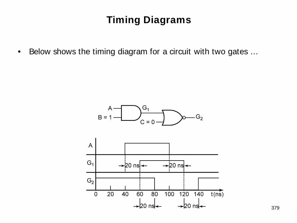
Division Method
BASE 10 FractionSuccessive Multiplication

67
Conversions Between
Two Bases
Conversions Between Two Bases
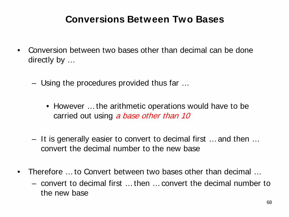
• Conversion between two bases other than decimal can be done directly by …
– Using the procedures provided thus far …
• However … the arithmetic operations would have to be carried out using a base other than 10
– It is generally easier to convert to decimal first … and then … convert the decimal number to the new base
• Therefore … to Convert between two bases other than decimal …– convert to decimal first … then … convert the decimal number to
the new base68
Conversions Between Two Bases
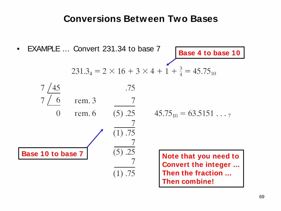
• EXAMPLE … Convert 231.34 to base 7
69
Base 4 to base 10
Base 10 to base 7 Note that you need toConvert the integer …Then the fraction …Then combine!
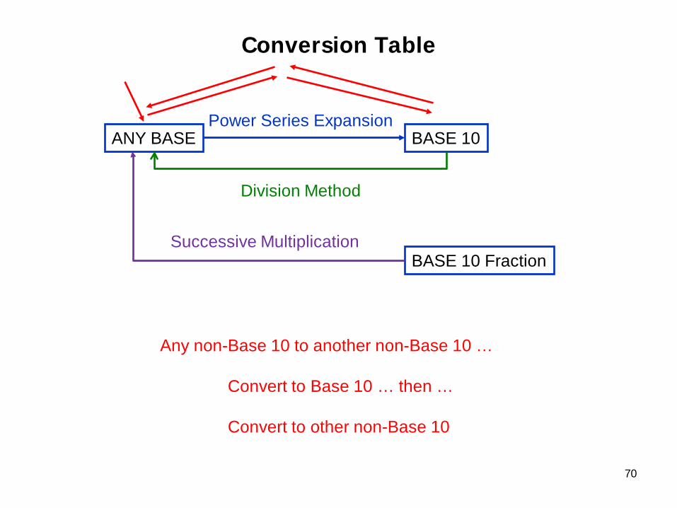
Conversion Table
70
ANY BASE BASE 10Power Series Expansion
Division Method
BASE 10 FractionSuccessive Multiplication
Any non-Base 10 to another non-Base 10 …
Convert to Base 10 … then …
Convert to other non-Base 10
71
Binaryto
Hexadecimal Conversions

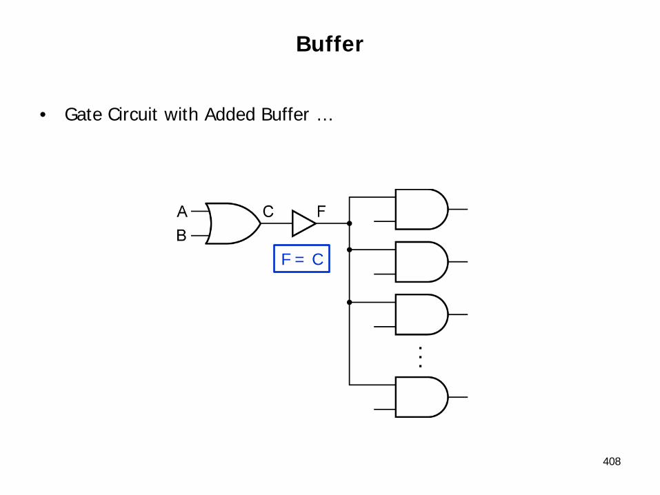
Binary Hexadecimal Conversion
• Conversion from binary to hexadecimal … and … conversely …
– Convert by inspection …
• Each hexadecimal digit corresponds to exactly four binary digits (bits)
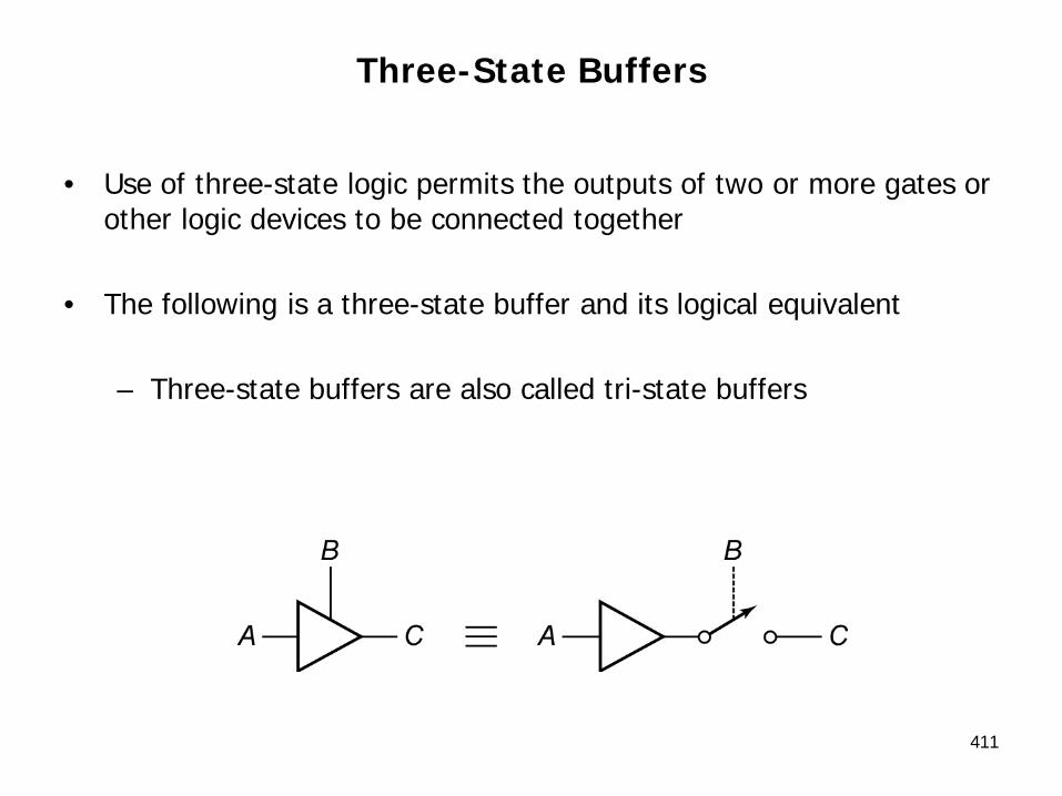
• Starting at the binary point …
– The bits are divided into groups of four– Each group is replaced by a hexadecimal digit
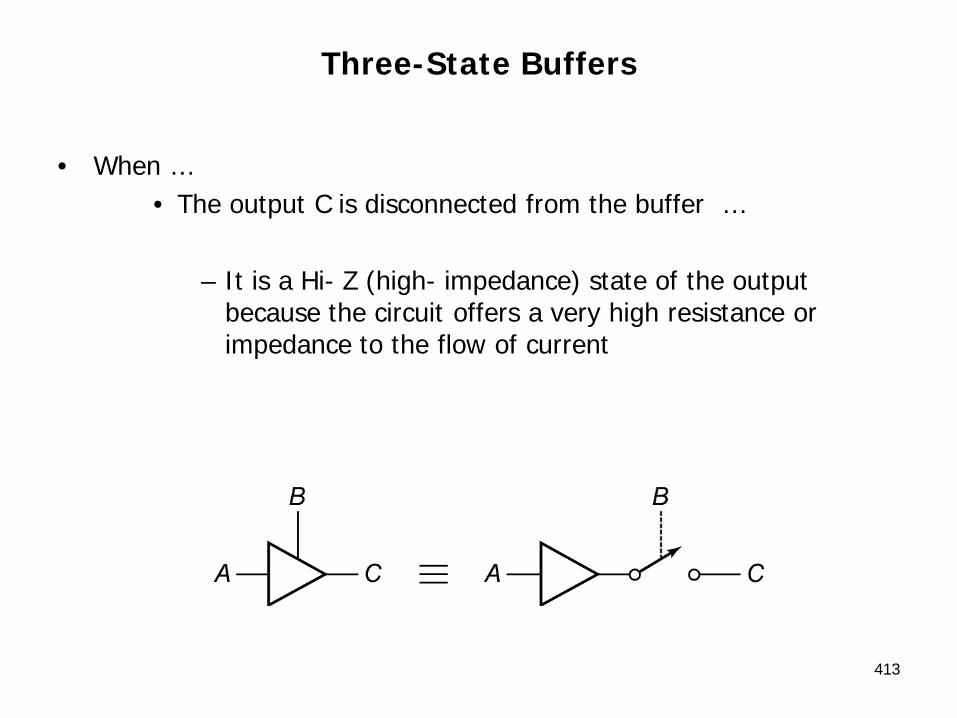
• Extra 0’s are added at each end of the bit string as needed to fill out the groups of four bits
72
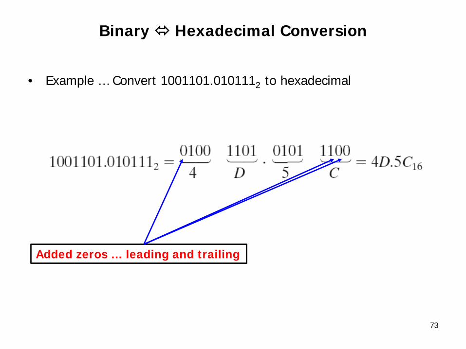
Binary Hexadecimal Conversion
• Example … Convert 1001101.0101112 to hexadecimal
73
Added zeros … leading and trailing
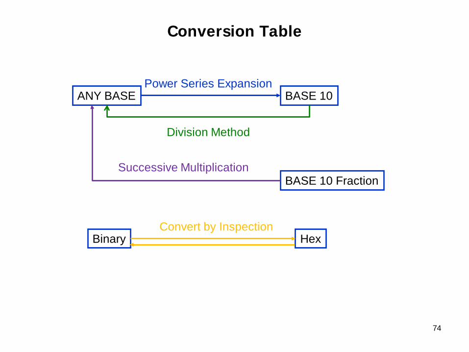
Conversion Table
74
ANY BASE BASE 10Power Series Expansion
Division Method
BASE 10 FractionSuccessive Multiplication
Binary HexConvert by Inspection

75
Summary …

Summary
• The Power Series Expansion can be used to convert to any base
• Division Method … the conversion of a decimal integer N to base RN = (a0a1a2….an)R
• Successive Multiplications … Conversion of a decimal fraction F to base R
• Conversion between two bases other than decimal … convert to decimal first … then … convert the decimal number to the new base
• Conversion from binary to hexadecimal … and … conversely … convert by inspection … Each hexadecimal digit corresponds to exactly four binary digits (bits)
76

Conversion Table
77
ANY BASE BASE 10Power Series Expansion
Division Method
BASE 10 FractionSuccessive Multiplication
Binary HexConvert by Inspection

78
Binary Arithmetic

Binary Arithmetic
• Arithmetic operations in digital systems are …
– Usually performed in binary
• The design of logic circuits to perform binary arithmetic is much easier than for decimal
79

80
Binary Addition
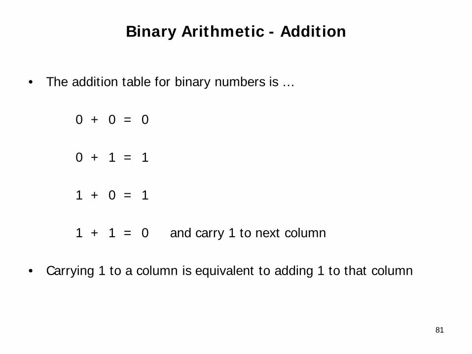
Binary Arithmetic - Addition
• The addition table for binary numbers is …
0 + 0 = 0
0 + 1 = 1
1 + 0 = 1
1 + 1 = 0 and carry 1 to next column
• Carrying 1 to a column is equivalent to adding 1 to that column
81

82
Binary Subtraction
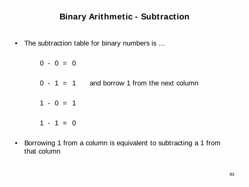
Binary Arithmetic - Subtraction
• The subtraction table for binary numbers is …
0 - 0 = 0
0 - 1 = 1 and borrow 1 from the next column
1 - 0 = 1
1 - 1 = 0
• Borrowing 1 from a column is equivalent to subtracting a 1 from that column
83

84
Binary Multiplication

Binary Arithmetic - Multiplication
• The multiplication table for binary numbers is …
0 x 0 = 00 x 1 = 01 x 0 = 01 x 1 = 1
85

• Example … multiply 1310 by 1110 in binary …
1310 = 11012
1110 =10112 … therefore …
X
Binary Arithmetic - Multiplication
86
X
Binary Arithmetic - Multiplication
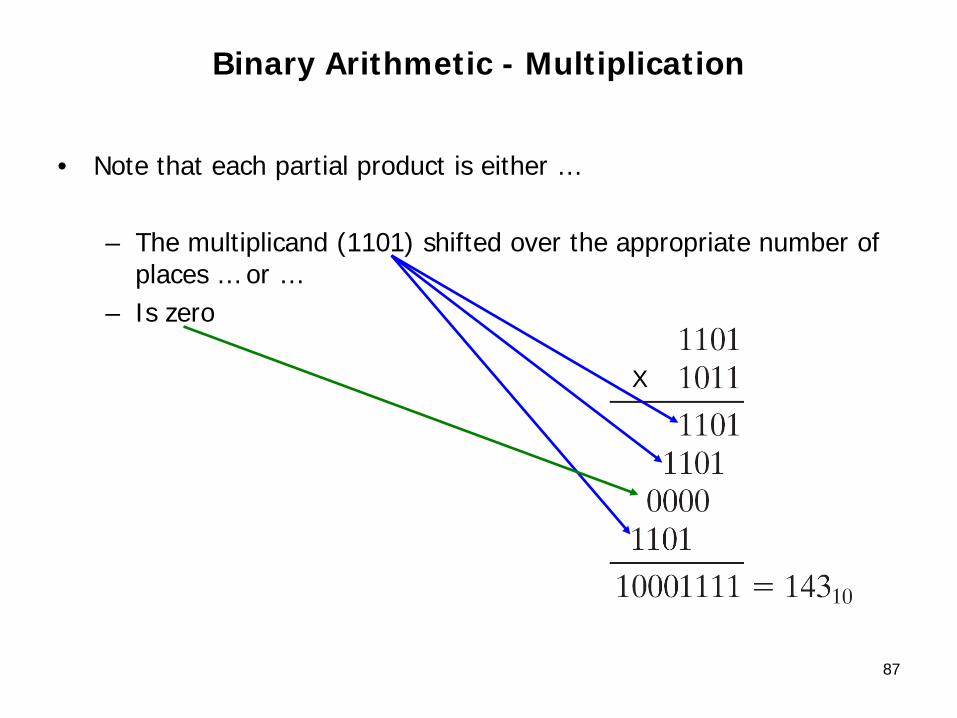
• Note that each partial product is either …
– The multiplicand (1101) shifted over the appropriate number of places … or …
– Is zero
87
Binary Arithmetic - Multiplication
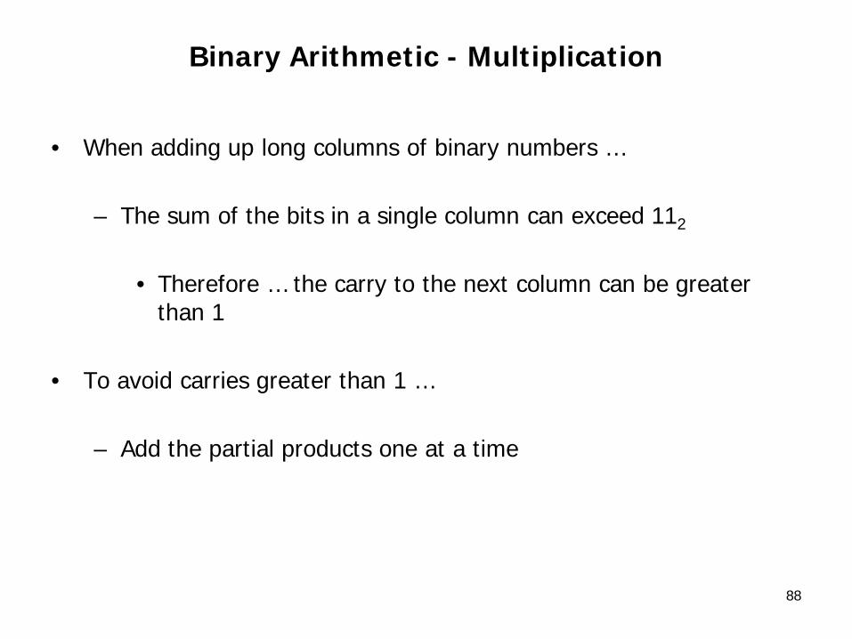
• When adding up long columns of binary numbers …
– The sum of the bits in a single column can exceed 112
• Therefore … the carry to the next column can be greater than 1
• To avoid carries greater than 1 …
– Add the partial products one at a time
88
Binary Arithmetic - Multiplication
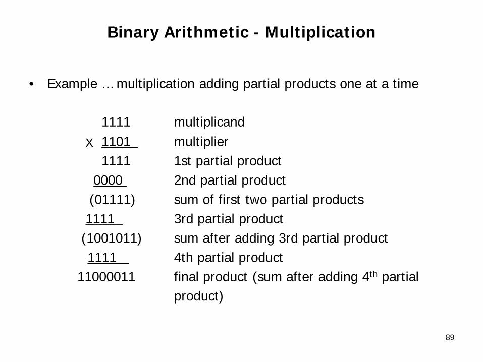
• Example … multiplication adding partial products one at a time
1111 multiplicand1101 multiplier1111 1st partial product
0000 2nd partial product(01111) sum of first two partial products1111 3rd partial product
(1001011) sum after adding 3rd partial product1111 4th partial product
11000011 final product (sum after adding 4th partialproduct)
89
X
90
Binary Division
Binary Arithmetic - Division
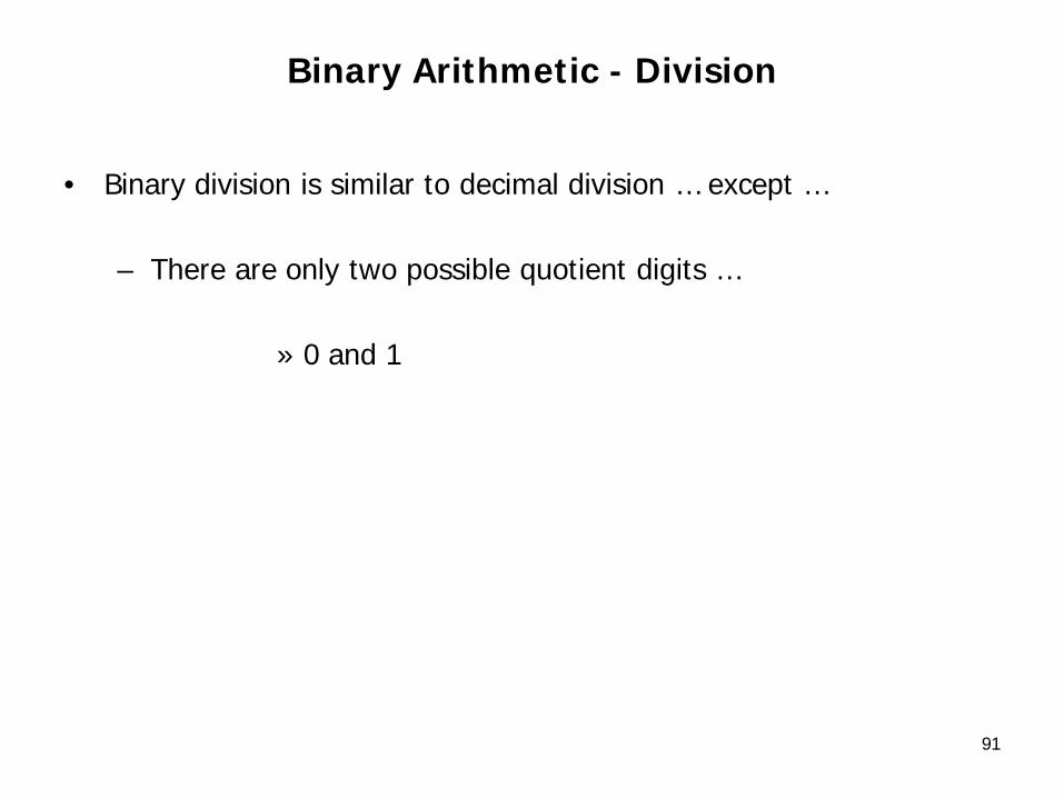
• Binary division is similar to decimal division … except …
– There are only two possible quotient digits …
» 0 and 1
91
Binary Arithmetic - Division
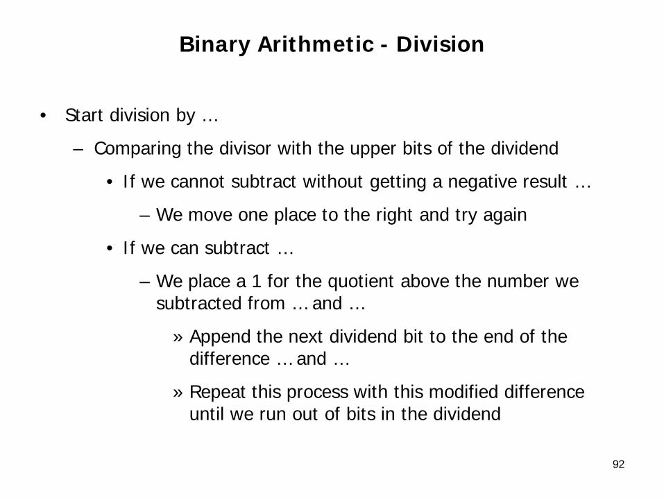
• Start division by …
– Comparing the divisor with the upper bits of the dividend
• If we cannot subtract without getting a negative result …
– We move one place to the right and try again
• If we can subtract …
– We place a 1 for the quotient above the number we subtracted from … and …
» Append the next dividend bit to the end of the difference … and …
» Repeat this process with this modified difference until we run out of bits in the dividend
92
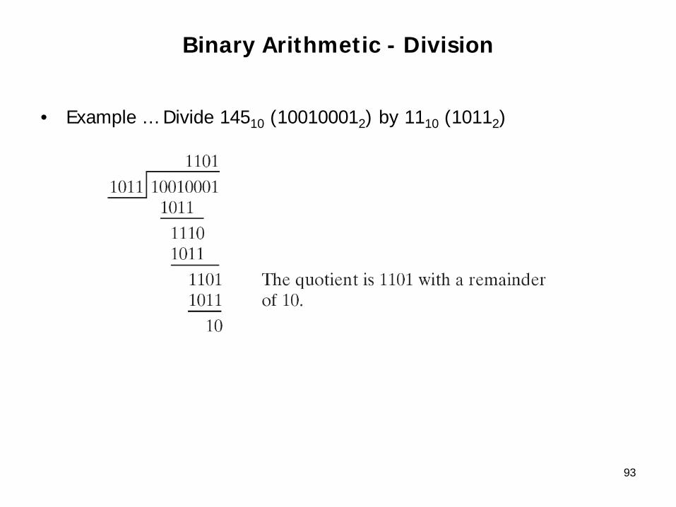
Binary Arithmetic - Division
• Example … Divide 14510 (100100012) by 1110 (10112)
93
94
Representation of Negative Numbers
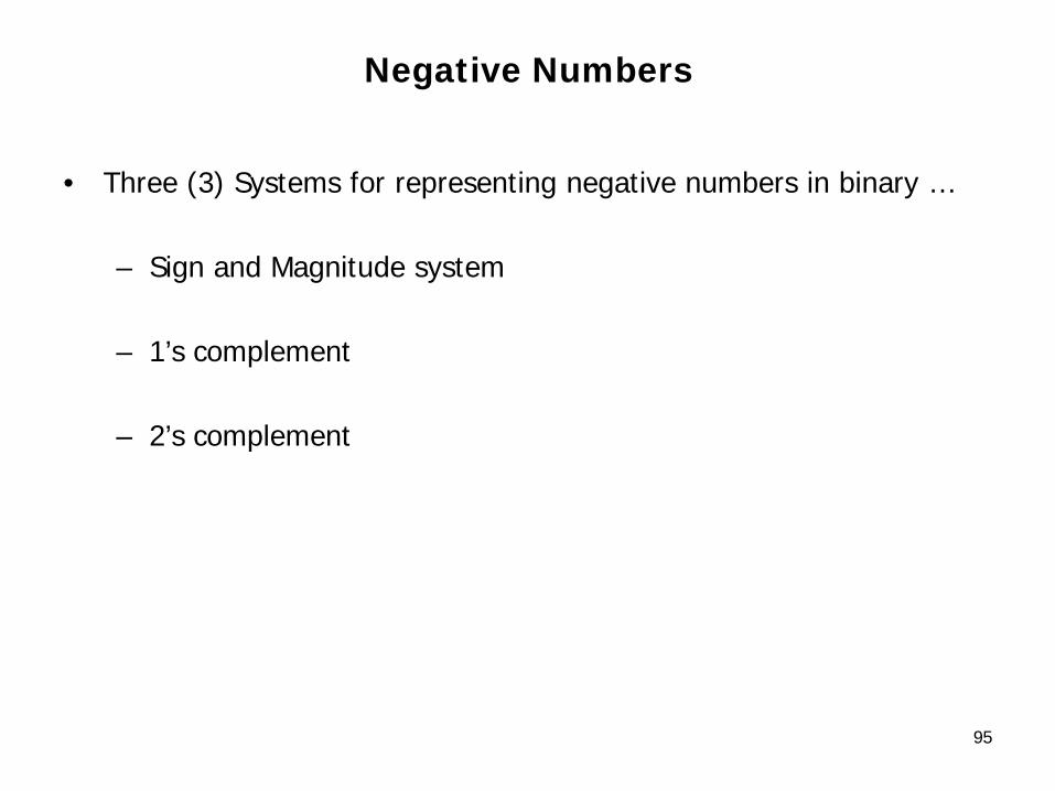
Negative Numbers
• Three (3) Systems for representing negative numbers in binary …
– Sign and Magnitude system
– 1’s complement
– 2’s complement
95

96
Negative Numbers - Sign and Magnitude

Negative Numbers - Sign and Magnitude
• Sign and Magnitude system …
– Most significant bit is the sign
• Example …
– 510 = 11012
97

98
Negative Numbers - 1’s Complement

Negative Numbers - 1’s Complement
• 1’s Complement …
– A negative number … – N
– Word length of … n bits
– 1’s complement … N
• 1’s complement is defined as …
N = (2n – 1) – N
99
Negative Numbers - 1’s Complement
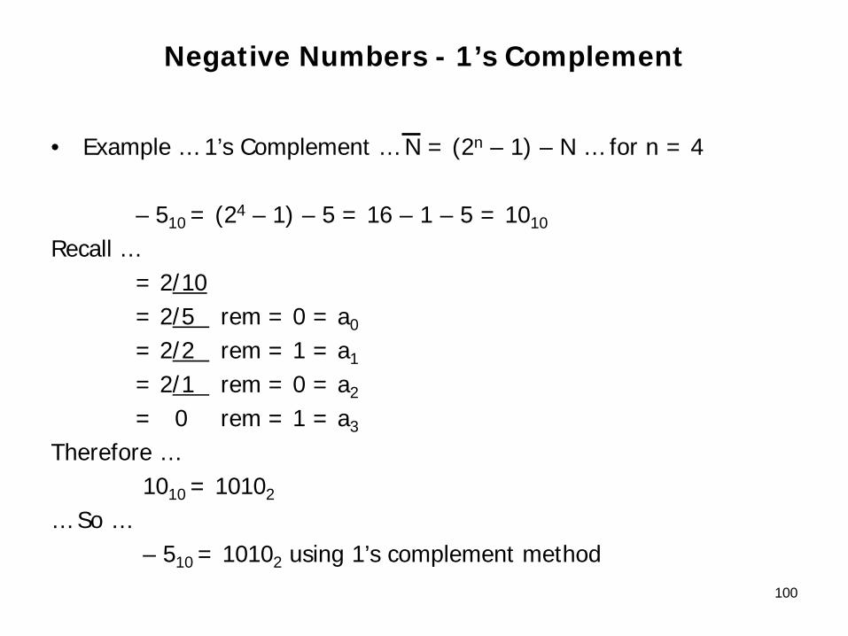
• Example … 1’s Complement … N = (2n – 1) – N … for n = 4
– 510 = (24 – 1) – 5 = 16 – 1 – 5 = 1010
Recall …= 2/10= 2/5 rem = 0 = a0
= 2/2 rem = 1 = a1
= 2/1 rem = 0 = a2
= 0 rem = 1 = a3
Therefore …1010 = 10102
… So …– 510 = 10102 using 1’s complement method
100
Negative Numbers - 1’s Complement
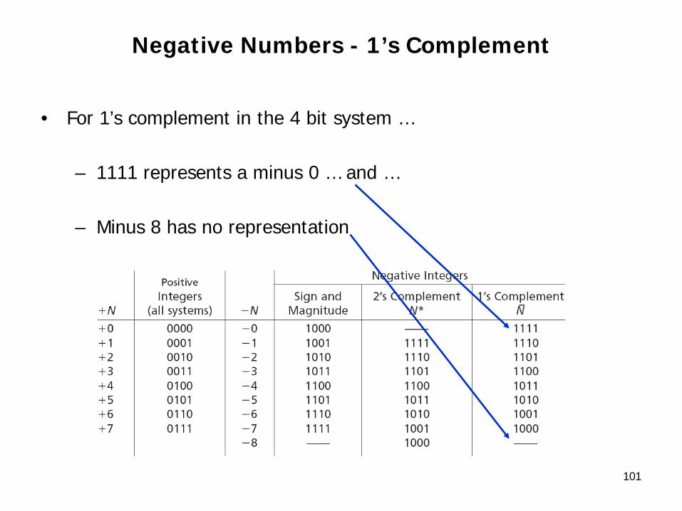
• For 1’s complement in the 4 bit system …
– 1111 represents a minus 0 … and …
– Minus 8 has no representation
101

Negative Numbers - 1’s Complement
• An alternate way to form the 1’ s complement is to …
– Complement N bit-by-bit by replacing 0’ s with 1’ s and 1’ s with 0’ s
• So … for N = 5 … the 1’s complement of N is found …
N = 0101 by using the alternate method abovereplacing 0’ s with 1’ s and 1’ s with 0’ s
N = 1010 … which is the same as previous example
102
103
Negative Numbers - 2’s Complement
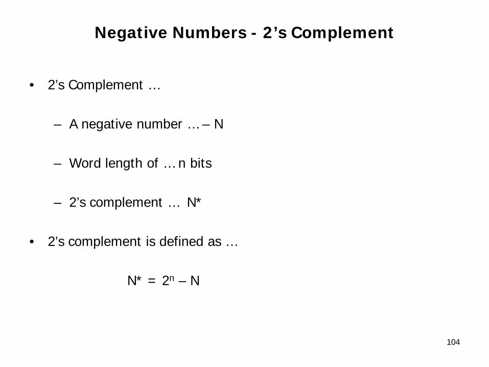
Negative Numbers - 2’s Complement
• 2’s Complement …
– A negative number … – N
– Word length of … n bits
– 2’s complement … N*
• 2’s complement is defined as …
N* = 2n – N
104
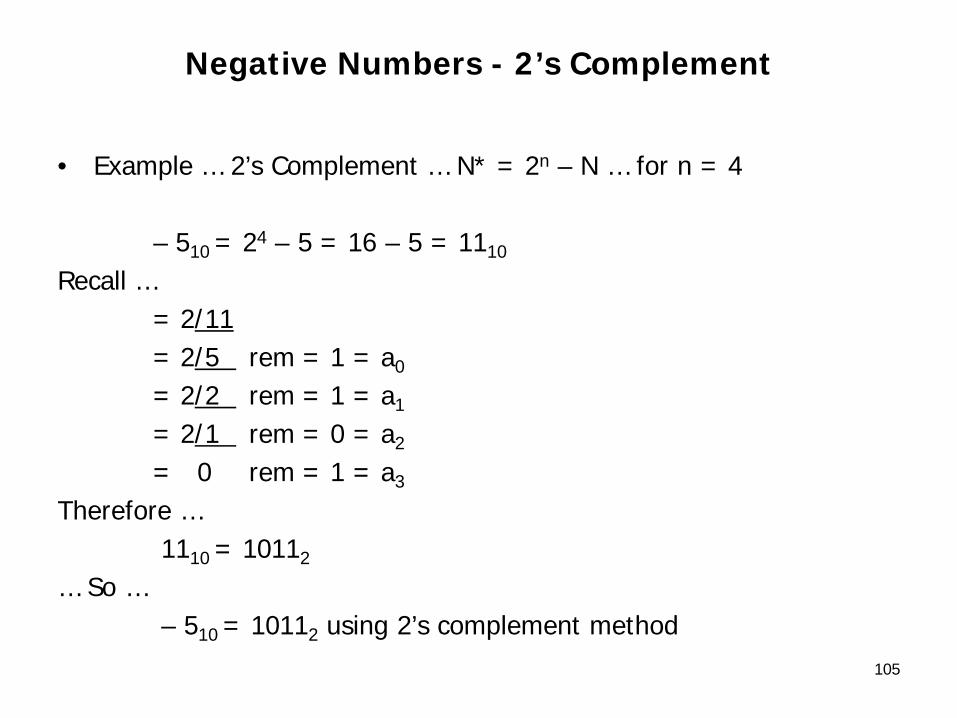
Negative Numbers - 2’s Complement
• Example … 2’s Complement … N* = 2n – N … for n = 4
– 510 = 24 – 5 = 16 – 5 = 1110
Recall …= 2/11= 2/5 rem = 1 = a0
= 2/2 rem = 1 = a1
= 2/1 rem = 0 = a2
= 0 rem = 1 = a3
Therefore …1110 = 10112
… So …– 510 = 10112 using 2’s complement method
105
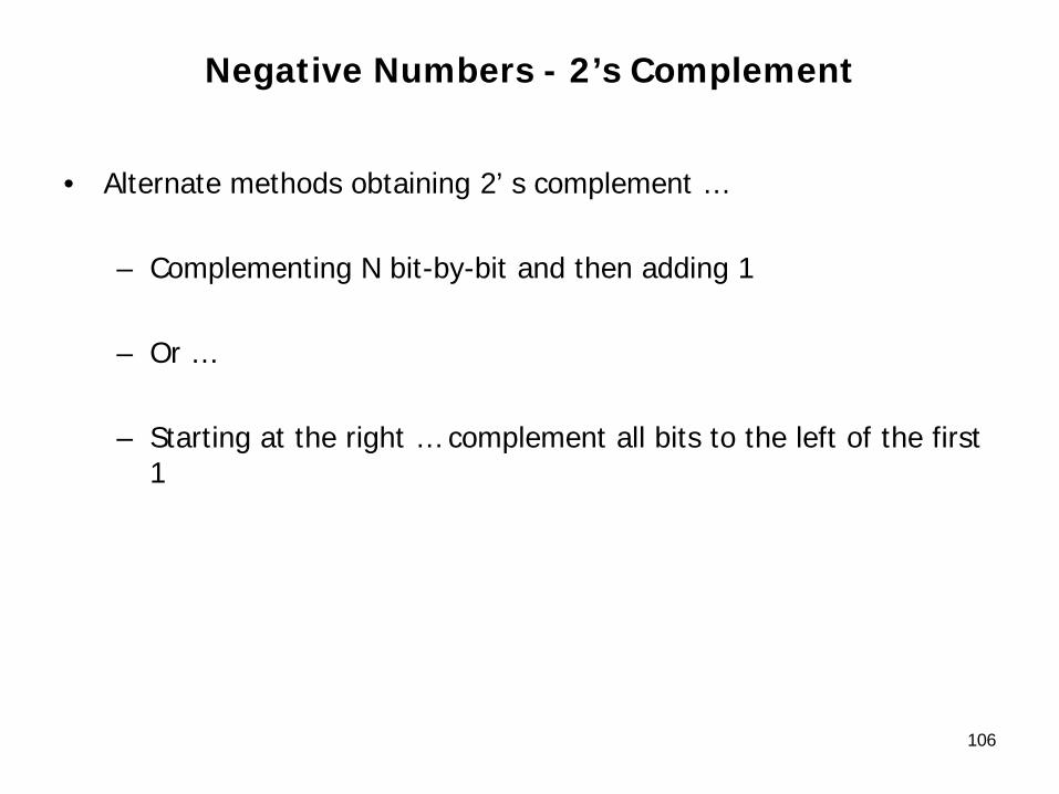
Negative Numbers - 2’s Complement
• Alternate methods obtaining 2’ s complement …
– Complementing N bit-by-bit and then adding 1
– Or …
– Starting at the right … complement all bits to the left of the first 1
106
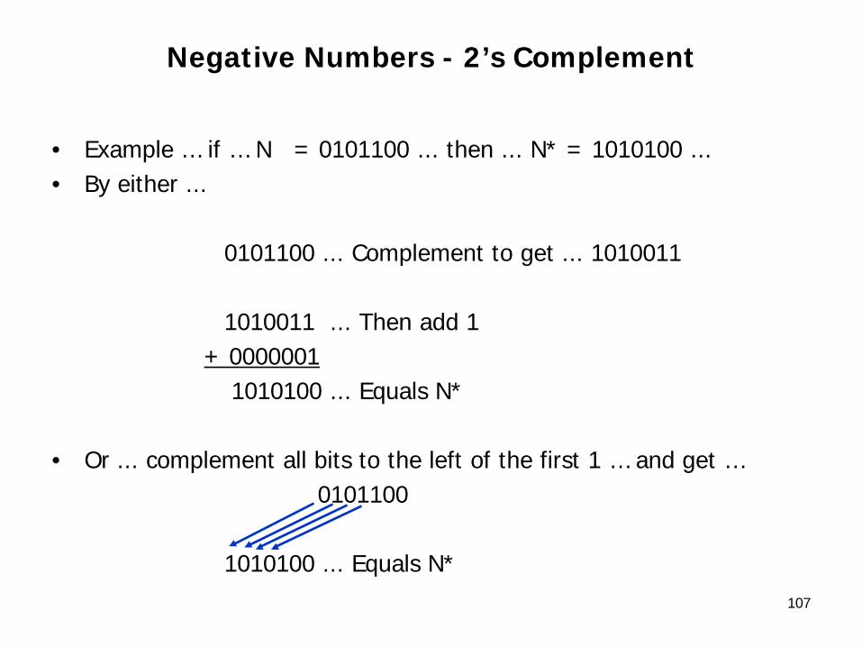
Negative Numbers - 2’s Complement
• Example … if … N = 0101100 ... then ... N* = 1010100 ... • By either ...
0101100 ... Complement to get ... 1010011
1010011 ... Then add 1+ 0000001
1010100 ... Equals N*
• Or ... complement all bits to the left of the first 1 … and get … 0101100
1010100 ... Equals N*107
108
Signed Binary Integers
(Word Length n = 4)
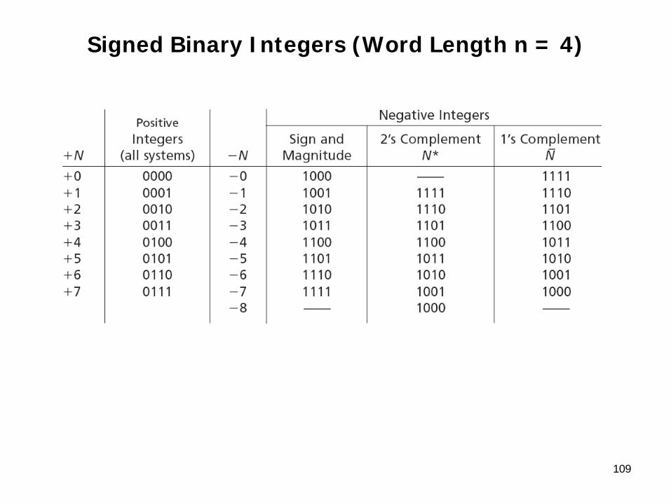
Signed Binary Integers (Word Length n = 4)
109
110
Determine Magnitude of Negative Numbers
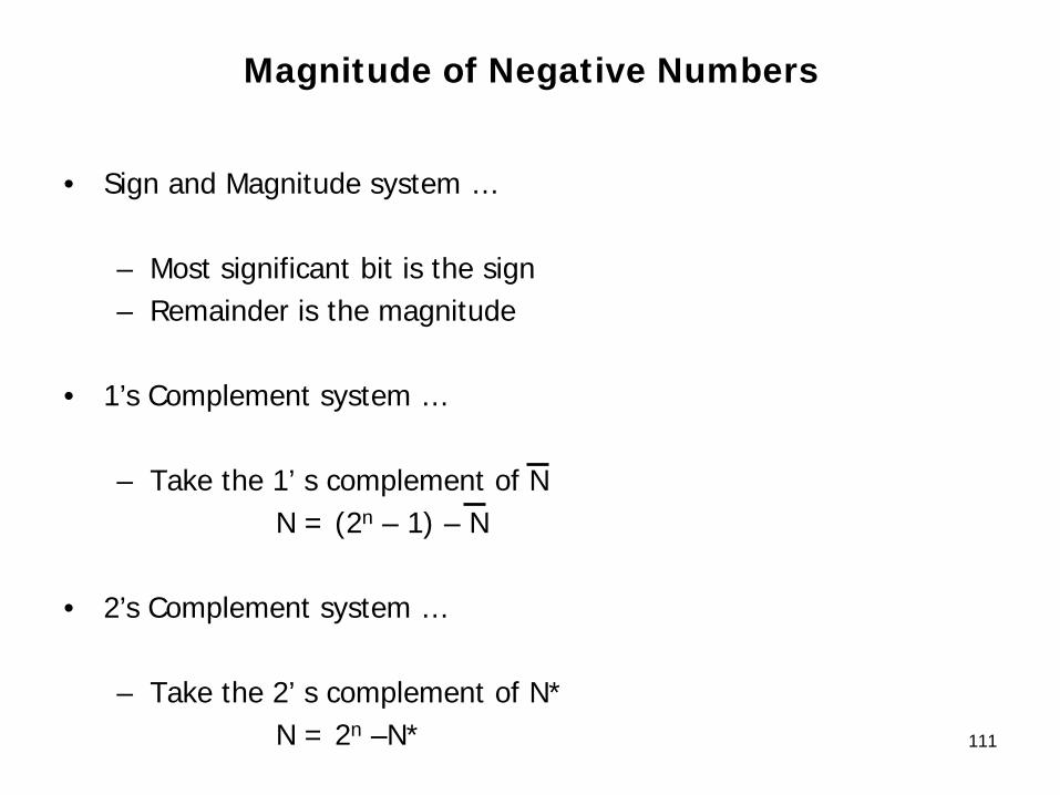
Magnitude of Negative Numbers
• Sign and Magnitude system …
– Most significant bit is the sign– Remainder is the magnitude
• 1’s Complement system …
– Take the 1’ s complement of NN = (2n – 1) – N
• 2’s Complement system …
– Take the 2’ s complement of N*N = 2n –N* 111

112
Addition of 2’s Complement Numbers
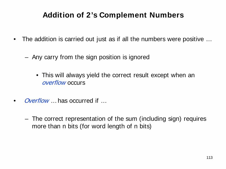
Addition of 2’s Complement Numbers
• The addition is carried out just as if all the numbers were positive …
– Any carry from the sign position is ignored
• This will always yield the correct result except when an overflow occurs
• Overflow … has occurred if …
– The correct representation of the sum (including sign) requires more than n bits (for word length of n bits)
113
Addition of 2’s Complement Numbers
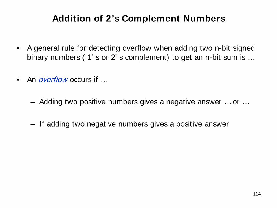
• A general rule for detecting overflow when adding two n-bit signed binary numbers ( 1’ s or 2’ s complement) to get an n-bit sum is …
• An overflow occurs if …
– Adding two positive numbers gives a negative answer … or …
– If adding two negative numbers gives a positive answer
114
115
Addition of 1’s Complement Numbers
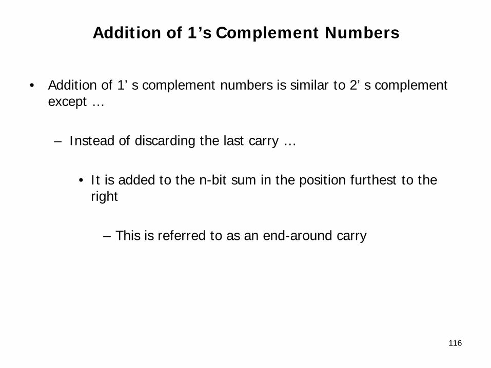
Addition of 1’s Complement Numbers
• Addition of 1’ s complement numbers is similar to 2’ s complement except …
– Instead of discarding the last carry …
• It is added to the n-bit sum in the position furthest to the right
– This is referred to as an end-around carry
116

Addition of 1’s Complement Numbers
• RECALL … A general rule for detecting overflow when adding two n-bit signed binary numbers ( 1’ s or 2’ s complement) to get an n-bit sum is …
• An overflow occurs if …
– Adding two positive numbers gives a negative answer … or …
– If adding two negative numbers gives a positive answer
117

118
Binary Codes

Binary Code
• Most computers work internally with binary numbers … however …
– Input-output equipment generally use decimal numbers
• Most logic circuits only accept two-valued signals … therefore …
– Decimal numbers must be coded in terms of binary signals
– In the simplest form of binary code, each decimal digit is replaced by its binary equivalent. For example, 937.25 is represented by:
119

Binary Code
• In the simplest form of binary code …
– Each decimal digit is replaced by its binary equivalent
• Example … 937.25 is represented by …
• The result is quite different than that obtained by converting the number as a whole into binary
120

121
Binary-Coded Decimal(BCD)

Binary-Coded Decimal - (BCD)
• The following representation is referred to as binary-coded-decimal (BCD) … or …
– 8-4-2-1 BCD
– There are only ten decimal digits … therefore …
• 1010 through 1111 are not valid BCD codes
122
123
Other Binary Codes
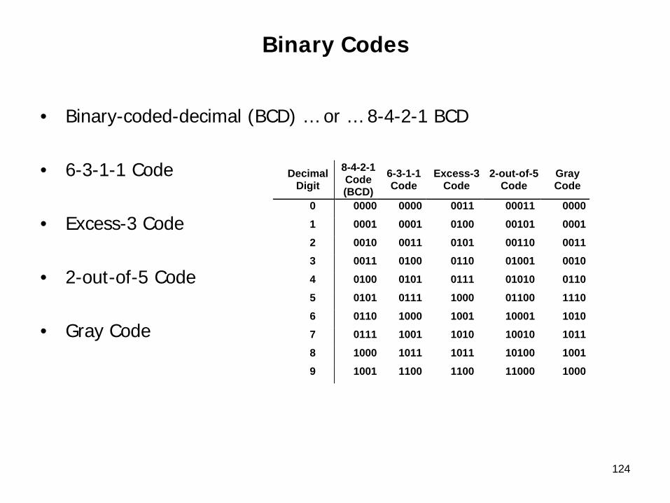
Binary Codes
• Binary-coded-decimal (BCD) … or … 8-4-2-1 BCD
• 6-3-1-1 Code
• Excess-3 Code
• 2-out-of-5 Code
• Gray Code
124
Decimal Digit
8-4-2-1 Code (BCD)
6-3-1-1 Code
Excess-3 Code
2-out-of-5 Code
Gray Code
0 0000 0000 0011 00011 0000
1 0001 0001 0100 00101 0001
2 0010 0011 0101 00110 0011 3 0011 0100 0110 01001 0010
4 0100 0101 0111 01010 0110
5 0101 0111 1000 01100 1110
6 0110 1000 1001 10001 1010 7 0111 1001 1010 10010 1011
8 1000 1011 1011 10100 1001
9 1001 1100 1100 11000 1000
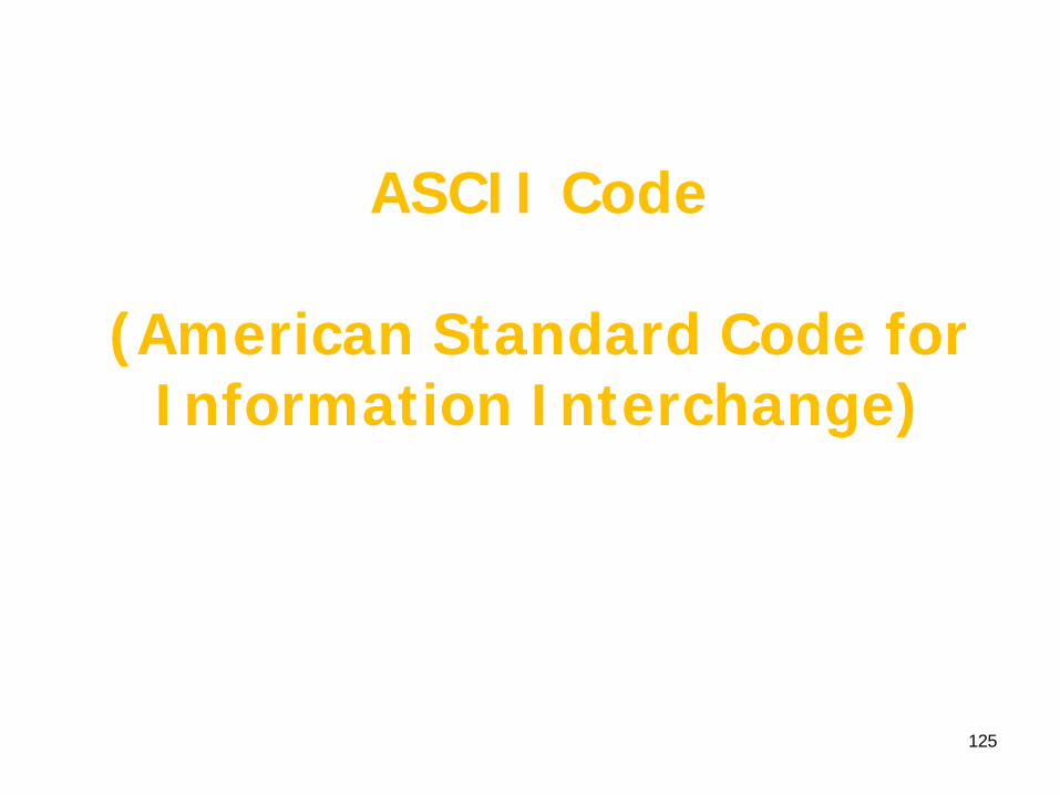
125
ASCII Code
(American Standard Code for Information Interchange)

ASCII Code
• ASCII Code (American Standard Code for Information Interchange)
– Many applications of computers require the processing of data which contains …
• Numbers, letters, and other symbols such as punctuation marks
– In order to transmit such alphanumeric data to or from a computer or store it internally in a computer …
• Each symbol must be represented by a binary code
126

ASCII Code
• A 7-bit code … therefore …
– 27 (128) different code combinations are available …
• They can represent …
– Letters
– Numbers
– And other symbols
127
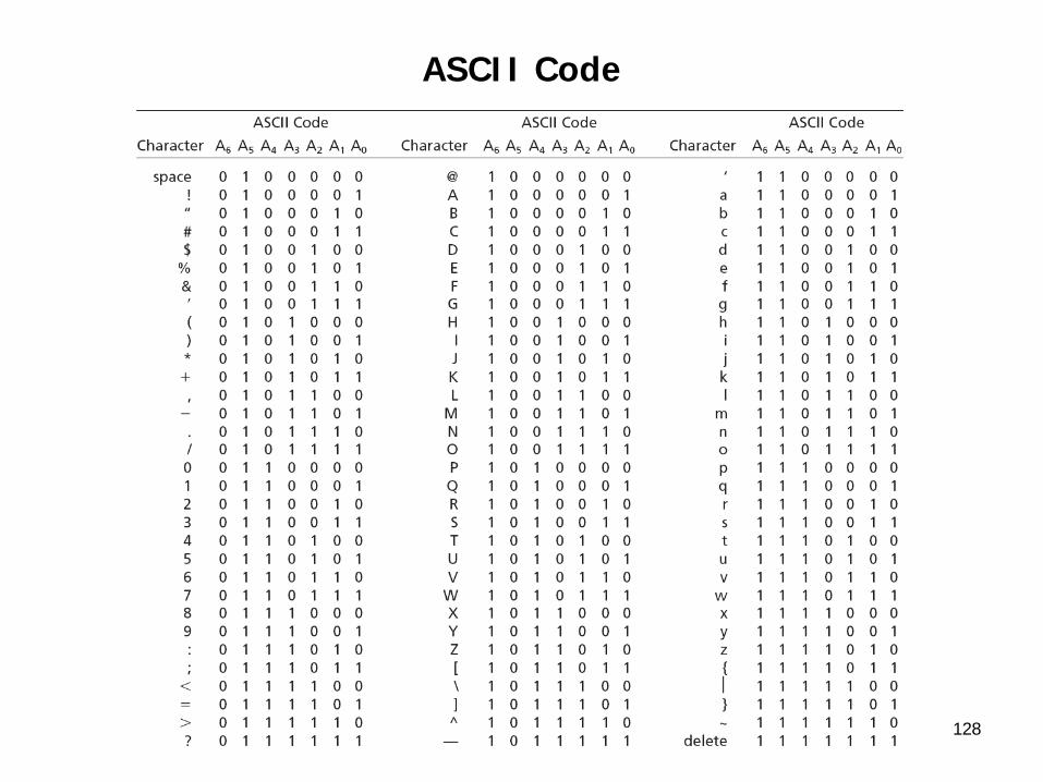
ASCII Code
128

129
Warning: Conversion or Coding?
• Do NOT mix up conversion of a decimal number to a binary number with coding a decimal number with a BINARY CODE
– 1310 = 11012 (This is conversion)
– 13 ⇔ 0001|0011 (This is coding)

130
Chapter 2 …
Boolean Algebra
Summary
• Laws and theorems of Boolean algebra
• We were able to …
1. Understand the basic operations and laws of Boolean algebra
2. Relate these operations and laws to … • Circuits composed of AND gates, OR gates, and INVERTERS• Circuits composed of switches
3. Prove any of these laws using a truth table
131

Summary
4. Applied laws to the manipulation of algebraic expressions including …
a) Multiplying out an expression to obtain a sum of products (SOP)
b) Factoring an expression to obtain a product of sums (POS)
c) Simplifying an expression by applying one of the laws
d) Finding the complement of an expression
132

133
Introduction
Introduction
• Boolean algebra …
– The basic mathematics needed for the study of the logic design of digital systems
• Switching circuits are essentially …
– Two-state devices …such as …
• A transistor with high or low output voltage
• We will study the special case of Boolean algebra in which all of the variables assume only one of two values … Referred to as switching algebra
134

Introduction
• Boolean variable … such as X or Y …
– Represents the input or output of a switching circuit
• Assume these variables can take on only two different values
– Symbols “ 0” and “ 1”
• If X is a Boolean (switching) variable …then …
– Either X = 0 … or … X = 1
135
Introduction
• Symbols “ 0” and “ 1” … do not …
– Have a numeric value
• They represent two different states
– In a logic gate circuit … “0” represents a range of low voltages … and …
– “1” represents a range of high voltages
136
Introduction
• For Switch circuits …
– “0” … represents an open switch … and … – “1” represents a closed circuit
• In general “0” and “1” can be used to represent …
– The two states in any binary-valued system
137

138
Basic Operations
Basic Operations
• Basic operations …
– AND
– OR
– Complement .. or … Inverse
139

140
Complement

Complement
• The complement of …
– 0 … is … 1
– 1 … is … 0
• Symbolically … where the prime (') denotes complementation
0' = 1
and
1' = 0 141

Complement
• X is a switching variable … therefore …
X' = 1 … if … X = 0
and
X' = 0 … if … X = 1
142
Complement
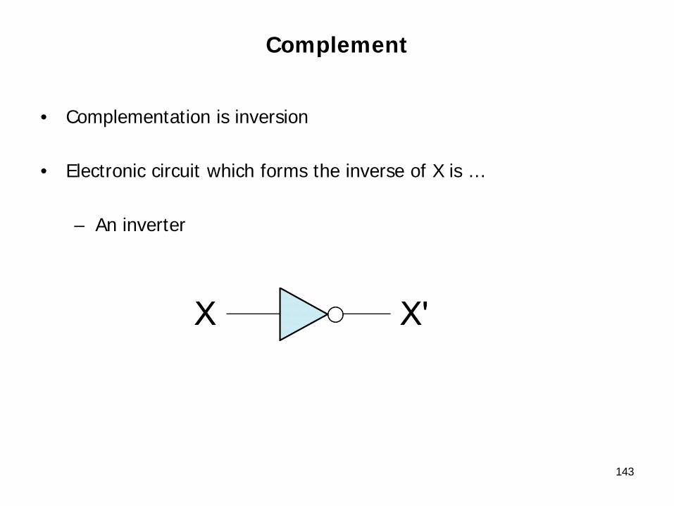
• Complementation is inversion
• Electronic circuit which forms the inverse of X is …
– An inverter
143

144
AND operation

AND operation
• The AND operation … where “•” denotes AND …
0 • 0 = 0 0 • 1 = 0 1 • 0 = 0 1 • 1 = 1
145
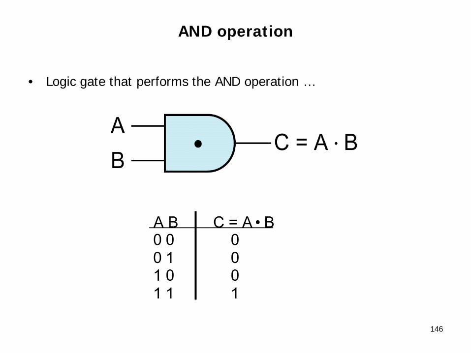
AND operation
• Logic gate that performs the AND operation …
146

147
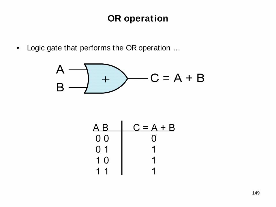
OR operation

OR operation
• The OR operation can be defined as follows …
0 + 0 = 0 0 + 1 = 1 1 + 0 = 1 1 + 1 = 1
• “+” denotes OR
148
OR operation
• Logic gate that performs the OR operation …
149

150
Switches

Switches
• Applying switching algebra to circuits containing switches
• Each switch is labeled with a variable
– If switch X is open … the value of X is 0
– If switch X is closed … the value of X is 1
151

Switches
• Therefore …
– Switches in a series perform the AND operation …
– Switches in parallel perform the OR operation
152
153
Boolean Expressions and
Truth Tables

154
Boolean Expressions

Boolean Expressions
• Boolean expressions are formed by …
– Application of the basic operations to one or more variables or constants
• The simplest expressions consist of a …
– Single constant or variable …
• 0• X• Y’
155

Boolean Expressions
• More complicated expressions are formed by …
– Combining two or more other expressions using …
» AND» OR» Or by complementing another expression
• Examples …
AB' + C
[A(C + D)]' + BE 156
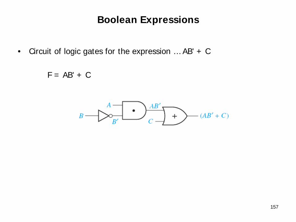
Boolean Expressions
• Circuit of logic gates for the expression … AB' + C
F = AB' + C
157
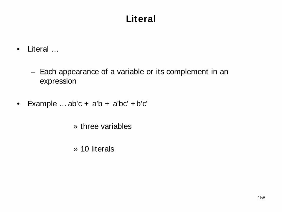
Literal
• Literal …
– Each appearance of a variable or its complement in an expression
• Example … ab'c + a’b + a’bc' +b’c'
» three variables
» 10 literals
158

159
Truth Table
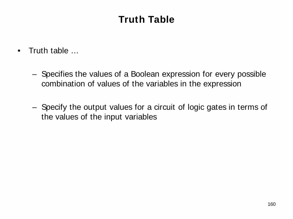
Truth Table
• Truth table …
– Specifies the values of a Boolean expression for every possible combination of values of the variables in the expression
– Specify the output values for a circuit of logic gates in terms of the values of the input variables
160
Truth Table
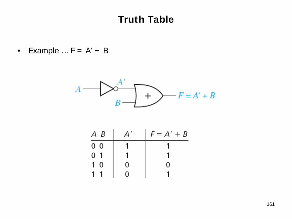
• Example … F = A’ + B
161
Truth Table
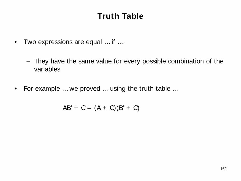
• Two expressions are equal … if …
– They have the same value for every possible combination of the variables
• For example … we proved … using the truth table …
AB’ + C = (A + C)(B’ + C)
162

Truth Table
• Prove … AB’ + C = (A + C)(B’ + C) … using the truth table …
Values for all 8 combinations are equal
163
A B C B’ AB’ AB’+C A+C B’+C (A+C)(B’+C) 0 0 0 1 0 0 0 1 0 0 0 1 1 0 1 1 1 1 0 1 0 0 0 0 0 0 0 0 1 1 0 0 1 1 1 1 1 0 0 1 1 1 1 1 1 1 0 1 1 1 1 1 1 1 1 1 0 0 0 0 1 0 0 1 1 1 0 0 1 1 1 1
164
Basic Theorems
165
Operations with 0 and 1
Theorem 2-4
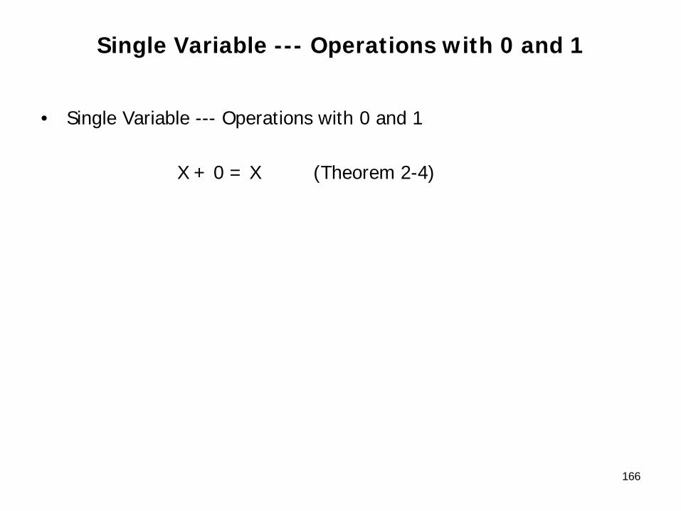
Single Variable --- Operations with 0 and 1
• Single Variable --- Operations with 0 and 1
X + 0 = X (Theorem 2-4)
166

167
Dual

Dual
• Dual …
– Is formed by replacing …
» AND with OR» OR with AND» 0 with 1» 1 with 0
– Variables and complements are left unchanged
168
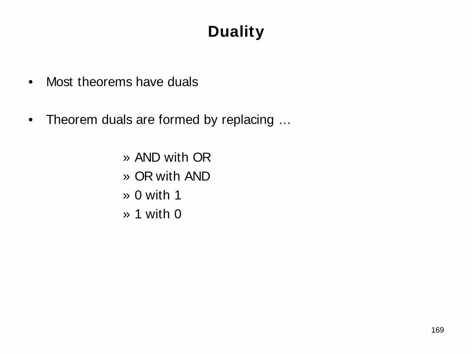
Duality
• Most theorems have duals
• Theorem duals are formed by replacing …
» AND with OR» OR with AND» 0 with 1» 1 with 0
169
170
Operations with 0 and 1
Theorem 2-4D

Single Variable --- Operations with 0 and 1
• Single Variable --- Operations with 0 and 1
X + 0 = X (2-4)
X • 1 = X (2-4D)
171

172
Operations with 0 and 1
Theorem 2-5
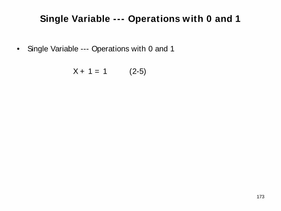
Single Variable --- Operations with 0 and 1
• Single Variable --- Operations with 0 and 1
X + 1 = 1 (2-5)
173

174
Operations with 0 and 1
Theorem 2-5D

Single Variable --- Operations with 0 and 1
• Single Variable --- Operations with 0 and 1
X + 1 = 1 (2-5)
X • 0 = 0 (2-5D)
175
176
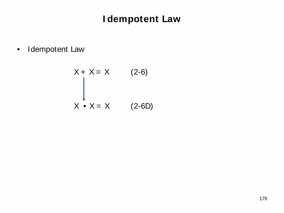
Idempotent Laws
Theorem 2-6
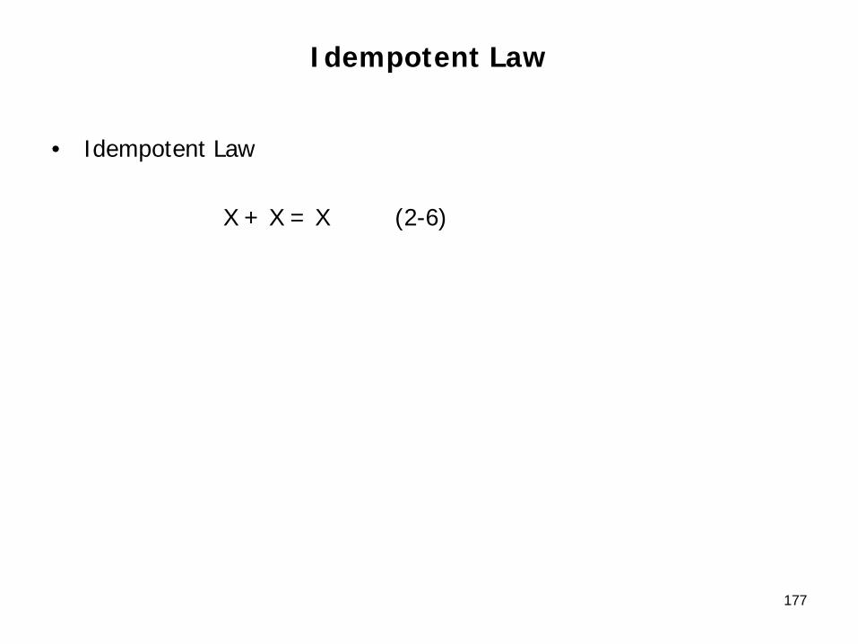
Idempotent Law
• Idempotent Law
X + X = X (2-6)
177

178
Idempotent Laws
Theorem 2-6D
Idempotent Law
• Idempotent Law
X + X = X (2-6)
X • X = X (2-6D)
179

180
Involution Law
Theorem 2-7

Involution Law
• Involution Law
(X’)’ = X (2-7)
• There is NO DUAL for 2-7
181

182
Laws of Complementarity
Theorem 2-8

Laws of Complementarity
• Laws of Complementarity
X + X’ = 1 (2-8)
183

184
Laws of Complementarity
Theorem 2-8D
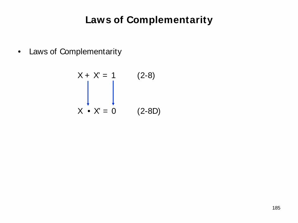
Laws of Complementarity
• Laws of Complementarity
X + X’ = 1 (2-8)
X • X’ = 0 (2-8D)
185
186
General Theorem
Information
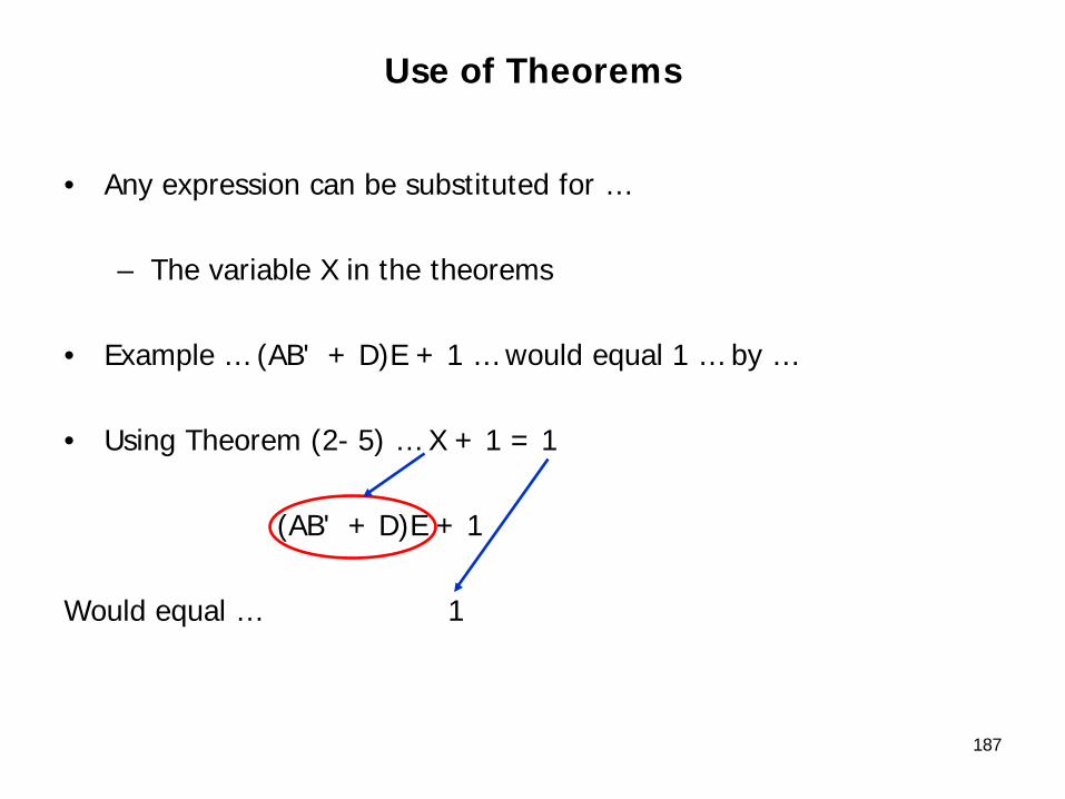
Use of Theorems
• Any expression can be substituted for …
– The variable X in the theorems
• Example … (AB' + D)E + 1 … would equal 1 … by …
• Using Theorem (2- 5) … X + 1 = 1
(AB' + D)E + 1
Would equal … 1
187
188
Commutative,Associative, and
Distributive Laws
Commutative, Associative, and Distributive Laws
• Many of the laws of ordinary algebra …such as …
– The commutative and associative laws …
• Also apply to Boolean algebra
189

190
Commutative Laws
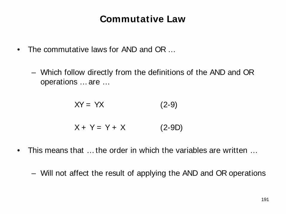
Commutative Law
• The commutative laws for AND and OR …
– Which follow directly from the definitions of the AND and OR operations … are …
XY = YX (2-9)
X + Y = Y + X (2-9D)
• This means that … the order in which the variables are written …
– Will not affect the result of applying the AND and OR operations
191

192
Associative Laws

Associative Laws
• The associate laws also apply to AND and OR …
(XY)Z = X(YZ) = XYZ (2-10)
(X + Y) + Z = X + (Y + Z) = X + Y + Z (2-10D)
193
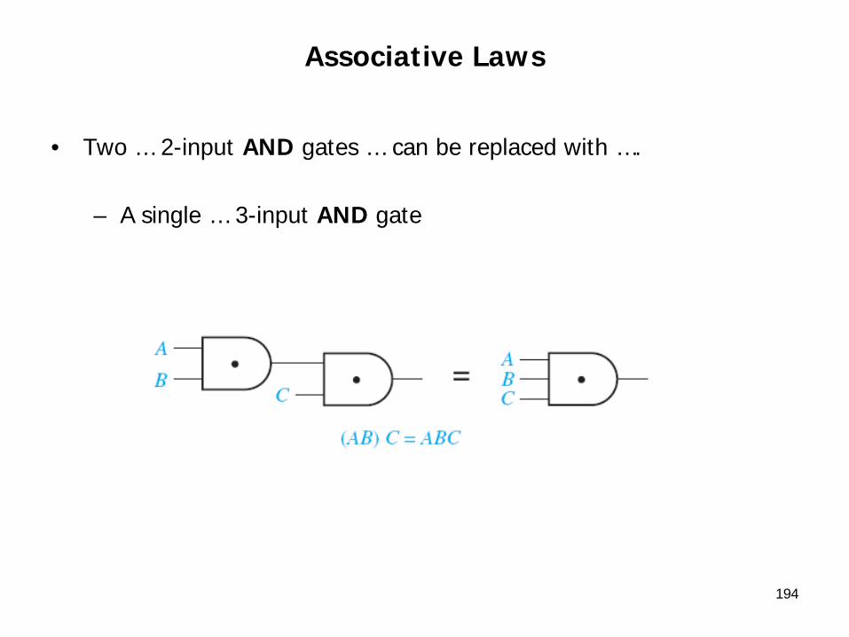
Associative Laws
• Two … 2-input AND gates … can be replaced with ….
– A single … 3-input AND gate
194

Associative Laws
• Two … 2-input OR gates … can be replaced with …
– A single … 3-input OR gate
195

Associative Laws
• When two or more variables are ANDed together …
– The value of the result will be 1 …
• iff … all of the variables have the value 1
– If any of the variables have the value 0 … then
• The result of the AND operation will be 0
196

Associative Laws
• When two or more variables are ORed together …
– The value of the result will be 1 if …
• Any of the variables have the value 1
– The result of the OR operation will be 0 …
• iff all of the variables have the value 0
197
198
Distributive Laws

Distributive Law
• Ordinary (algebra) distributive law …
X(Y + Z) = XY + XZ
– The ordinary distributive law states that …
• The AND operation distributes over OR
199
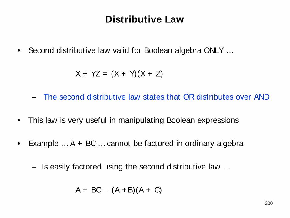
Distributive Law
• Second distributive law valid for Boolean algebra ONLY …
X + YZ = (X + Y)(X + Z)
– The second distributive law states that OR distributes over AND
• This law is very useful in manipulating Boolean expressions
• Example … A + BC … cannot be factored in ordinary algebra
– Is easily factored using the second distributive law …
A + BC = (A +B)(A + C)200
201
Simplification Theorems

Simplification Theorems
• The following theorems are useful in simplifying Boolean expressions …
XY + XY’ = X (2-12) (X + Y)(X + Y’) = X (2-12D)
X + XY = X (2-13) X(X + Y) = X (2-13D)
(X + Y’)Y = XY (2-14) XY’ + Y = X + Y (2-14D)
202

203
Multiplying Out
and
Factoring

204
Sum-Of-Products (SOP) …
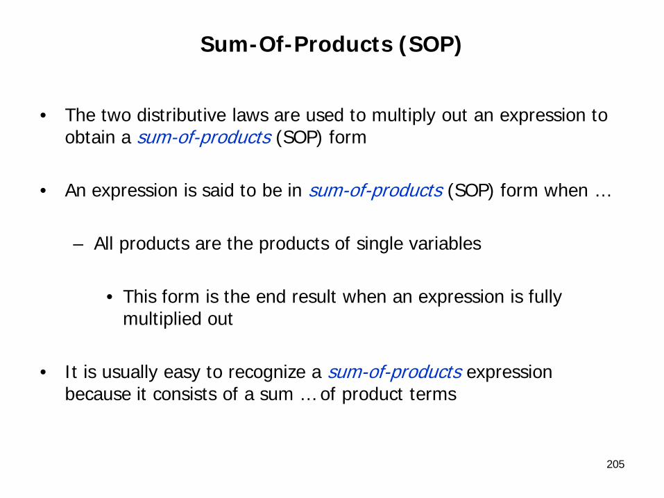
Sum-Of-Products (SOP)
• The two distributive laws are used to multiply out an expression to obtain a sum-of-products (SOP) form
• An expression is said to be in sum-of-products (SOP) form when …
– All products are the products of single variables
• This form is the end result when an expression is fully multiplied out
• It is usually easy to recognize a sum-of-products expression because it consists of a sum … of product terms
205

Sum-Of-Products (SOP)
• Sum-of-products examples …
AB’ + CD’E + AC’E’
A + B’ + C + D’E “degenerated” example
• Examples that are NOT sum-of-products
(A + B)CD + EF (A + B) is not a single variable
206

Sum-Of-Products (SOP)
• A sum-of-products expression can always be realized directly by …
– One or more AND gates feeding a single OR gate at the circuit output
207
Sum-Of-Products (SOP)
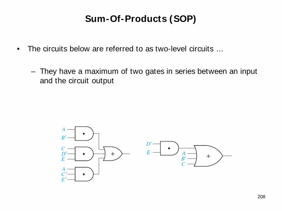
• The circuits below are referred to as two-level circuits …
– They have a maximum of two gates in series between an input and the circuit output
208

209
Product-Of-Sums (POS) …

Product-Of-Sums (POS)
• Both distributive laws can be used to factor an expression to obtain a product-of-sums form
• An expression is in product-of-sums (POS) form when …
– All sums are the sums of single variables
• It is usually easy to recognize a product-of-sums expression since it consists of a product … of sum terms
210
Product-Of-Sums (POS)
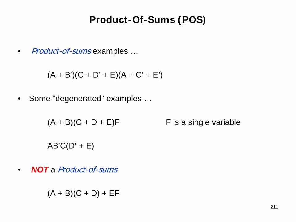
• Product-of-sums examples …
(A + B’)(C + D’ + E)(A + C’ + E’)
• Some “degenerated” examples …
(A + B)(C + D + E)F F is a single variable
AB’C(D’ + E)
• NOT a Product-of-sums
(A + B)(C + D) + EF211
Product-Of-Sums (POS)
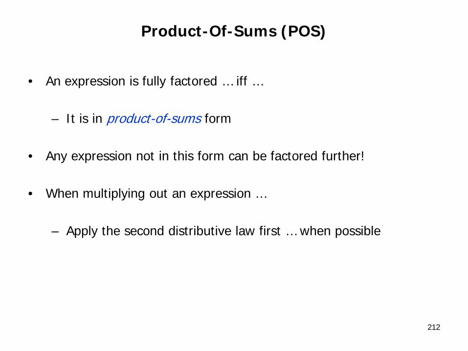
• An expression is fully factored … iff …
– It is in product-of-sums form
• Any expression not in this form can be factored further!
• When multiplying out an expression …
– Apply the second distributive law first … when possible
212

Product-Of-Sums (POS)
• A product-of-sums expression can always be realized directly by …
– One or more OR gates feeding a single AND gate at the circuit output
• The circuits below are referred to as two- level circuits because they have a maximum of two gates in series between an input and the circuit output
213

214
DeMorgan’s Laws
DeMorgan’s Laws
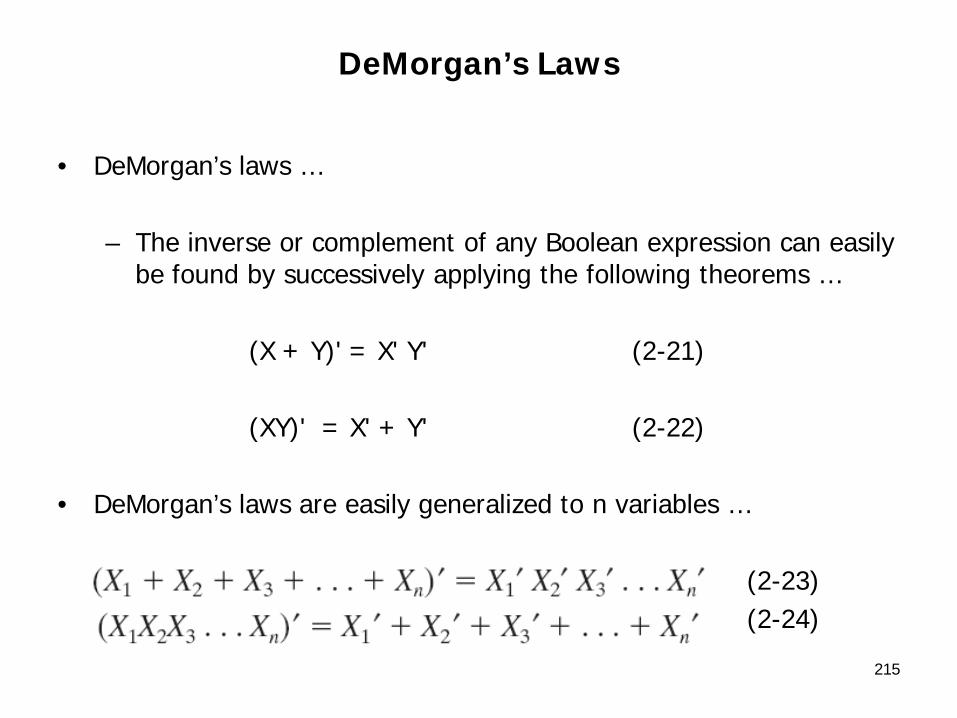
• DeMorgan’s laws …
– The inverse or complement of any Boolean expression can easily be found by successively applying the following theorems …
(X + Y)' = X' Y' (2-21)
(XY)' = X' + Y' (2-22)
• DeMorgan’s laws are easily generalized to n variables …
(2-23)(2-24)
215

DeMorgan’s Laws
• Referring to the …
– OR operation as the logical sum … and …
– The AND operation as logical product …
• DeMorgan’s laws can be stated as …
– The complement of the product is the sum of the complements– The complement of the sum is the product of the complements
• To form the complement of an expression containing both OR and AND operations … DeMorgan’s laws are applied alternately
216

217
LAWS AND THEOREMS
Page 55

218

219
Chapter 3 …
Boolean Algebra(Continued)
Summary
• Understand and apply Chapter 2 Boolean algebra Laws and Theorems
– Applied laws and theorems to the manipulation of algebraic expressions including …
• Simplifying an expression
• Finding the complement of an expression
• Multiplying out and factoring an expression
220

Summary
• Continued …
– Proved theorems using a truth table or algebraic proof
– Defined the exclusive-OR and equivalence operations
– Use the consensus theorem to delete terms from and add terms to a switching expression
– Given an equation … • Proved algebraically that it is valid … or …
• Showed that it is not valid
221
222
Multiplying Outand
Factoring Expressions

223
Multiplying Out

Multiplying Out
• Given an expression in product-of-sums form …
– The corresponding sum-of-products expression can be obtained by …
– Multiplying out … using … the following two distributive laws …
X(Y + Z) = XY + XZ (3-1)
(X + Y)(X + Z) = X + YZ (3-2)
224
Multiplying Out
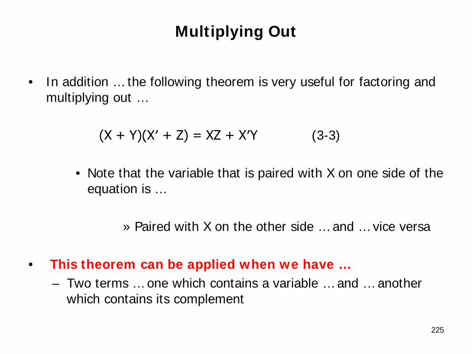
• In addition … the following theorem is very useful for factoring and multiplying out …
(X + Y)(X′ + Z) = XZ + X′Y (3-3)
• Note that the variable that is paired with X on one side of the equation is …
» Paired with X on the other side … and … vice versa
• This theorem can be applied when we have …– Two terms … one which contains a variable … and … another
which contains its complement
225
226
Factoring
Factoring
• Any expression can be converted to a product-of-sums form by using …
– The same theorems that are useful for multiplying out expressions … By …
• Repeatedly applying … (3-1) … (3-2) … and (3-3)
X(Y + Z) = XY + XZ (3-1)
(X + Y)(X + Z) = X + YZ (3-2)
(X + Y)(X′ + Z) = XZ + X′Y (3-3)
227
228
Exclusive-OR
and
Equivalence Operations

229
Exclusive-OR

• The exclusive-OR operation ( ) is defined as follows …
Exclusive-OR
230
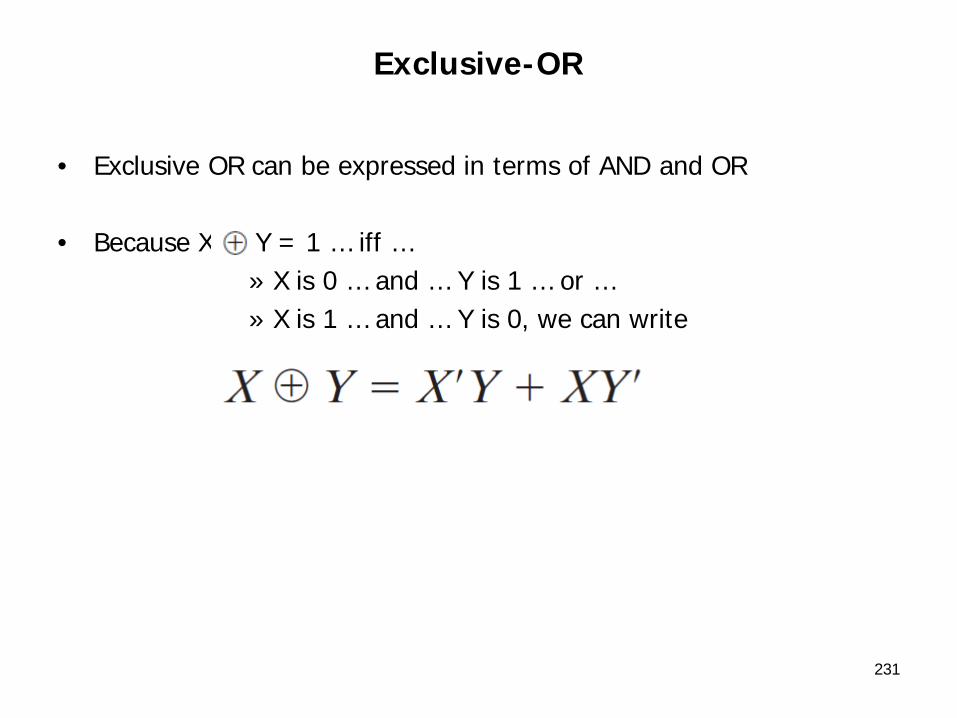
• Exclusive OR can be expressed in terms of AND and OR
• Because X Y = 1 … iff …» X is 0 … and … Y is 1 … or …» X is 1 … and … Y is 0, we can write
Exclusive-OR
231
Exclusive-OR
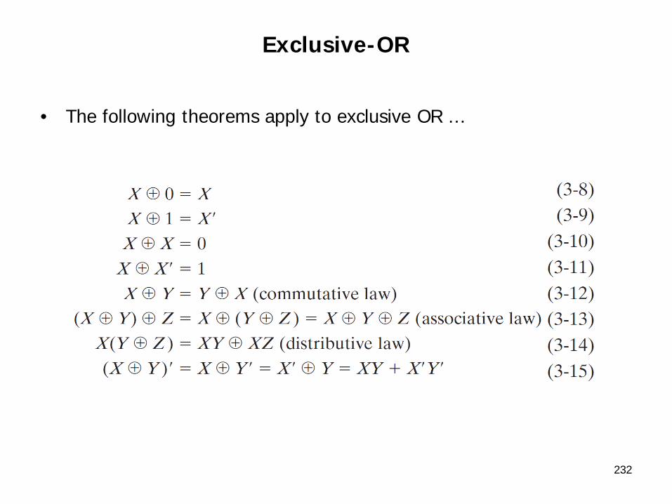
• The following theorems apply to exclusive OR …
232
233
Equivalence Operations
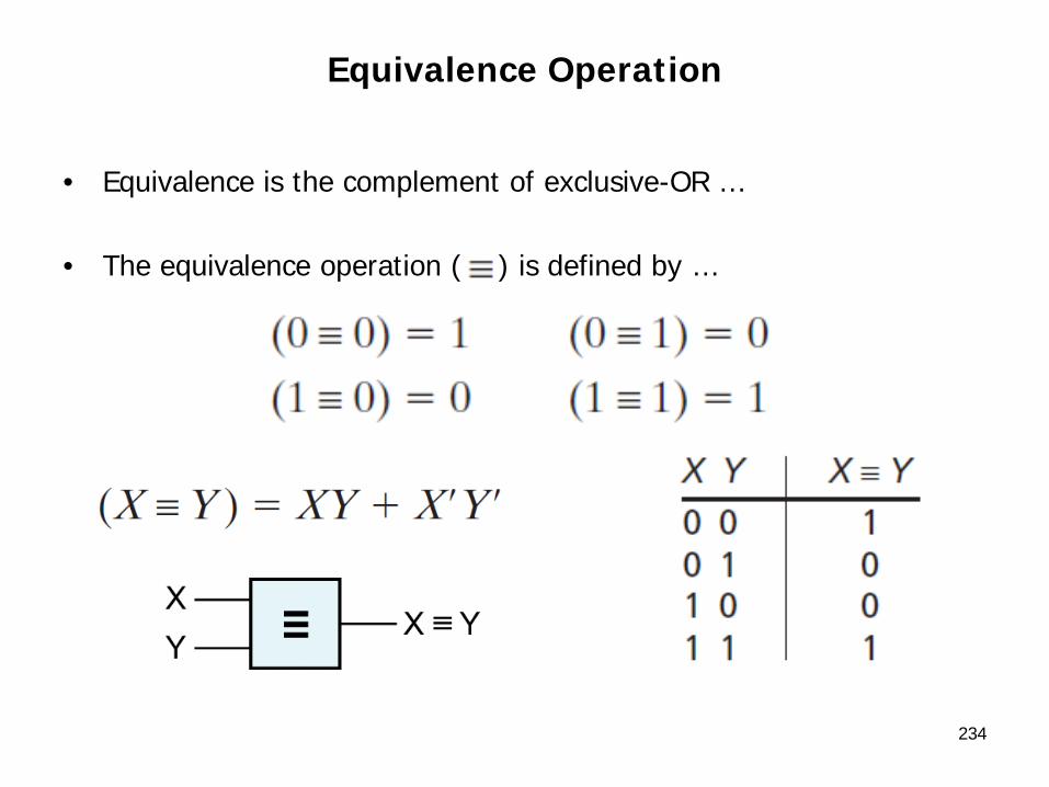
Equivalence Operation
• Equivalence is the complement of exclusive-OR …
• The equivalence operation ( ) is defined by …
234
Equivalence Operation
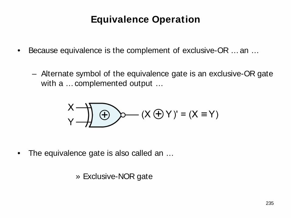
• Because equivalence is the complement of exclusive-OR … an …
– Alternate symbol of the equivalence gate is an exclusive-OR gate with a … complemented output …
• The equivalence gate is also called an …
» Exclusive-NOR gate
235

236
The Consensus Theorem

Consensus Theorem
• The consensus theorem is very useful in simplifying Boolean expressions
• Given an expression of the form …
• The term YZ is redundant … and …
– Can be eliminated to form the equivalent expression …
– The term that was eliminated is referred to as the consensus term
237
XY + X'Z + YZ
XY + X'Z
Consensus Theorem
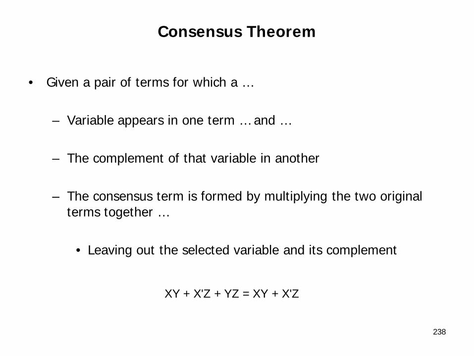
• Given a pair of terms for which a …
– Variable appears in one term … and …
– The complement of that variable in another
– The consensus term is formed by multiplying the two original terms together …
• Leaving out the selected variable and its complement
238
XY + X'Z + YZ = XY + X'Z
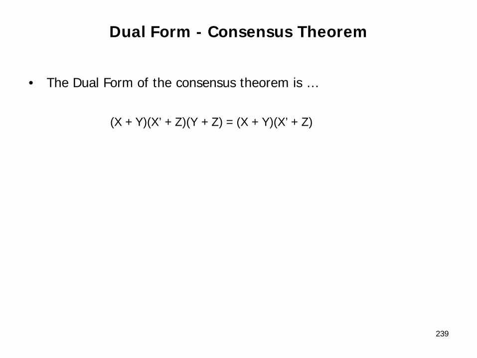
Dual Form - Consensus Theorem
• The Dual Form of the consensus theorem is …
239
(X + Y)(X’ + Z)(Y + Z) = (X + Y)(X’ + Z)

240
Basic Methods
for
Simplifying Functions
241
Combining Terms
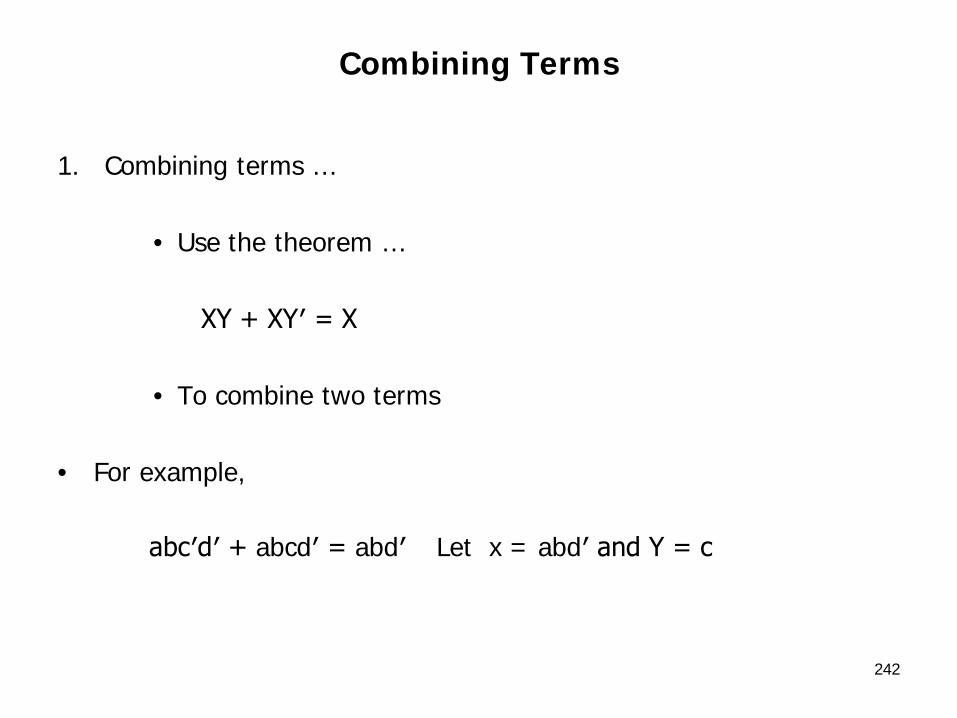
Combining Terms
1. Combining terms …
• Use the theorem …
XY + XY′ = X
• To combine two terms
• For example,
242
abc′d′ + abcd′ = abd′ Let x = abd′ and Y = c

243
Eliminating Terms

Eliminating Terms
2. Eliminating terms …
– Use the theorem …
X + XY = X
• To eliminate redundant terms if possible … then …
• Try to apply the consensus theorem …
XY + X′Z + YZ = XY + X′Z
• To eliminate any consensus terms244

245
Eliminating Literals

Eliminating Literals
3. Eliminating literals …
– Use the theorem …
X + X’Y = X + Y
– … To eliminate redundant literals
– Simple factoring may be necessary before the theorem is applied
246

247
Adding Redundant Terms
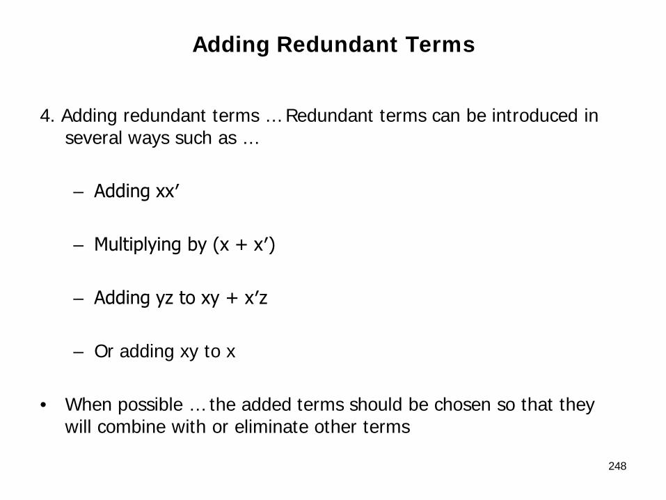
Adding Redundant Terms
4. Adding redundant terms … Redundant terms can be introduced in several ways such as …
– Adding xx′
– Multiplying by (x + x′)
– Adding yz to xy + x′z
– Or adding xy to x
• When possible … the added terms should be chosen so that they will combine with or eliminate other terms
248

249
Chapter 4 …
APPLICATIONS OF BOOLEAN ALGEBRA
MINTERM AND MAXTERM EXPANSIONS
Applying Boolean Algebra
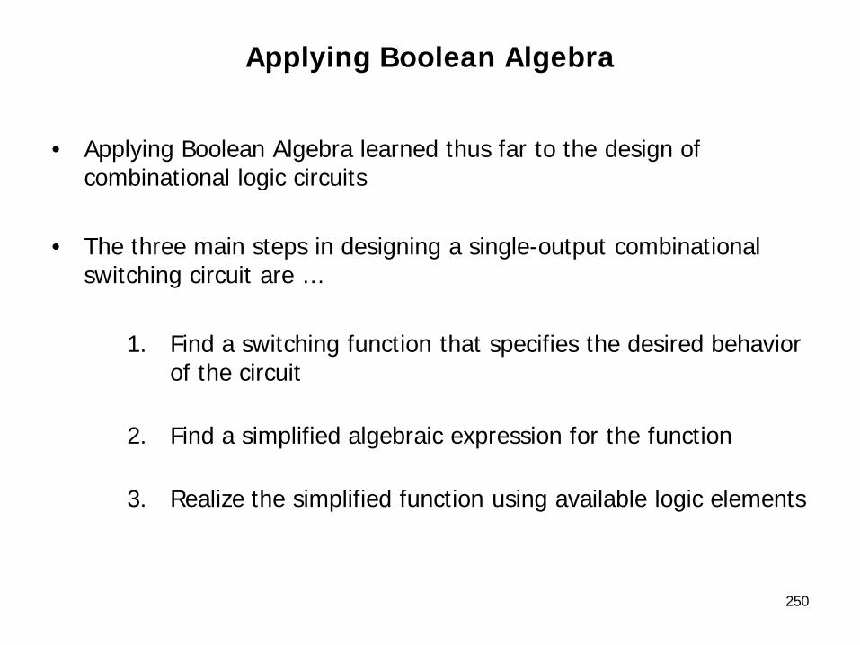
• Applying Boolean Algebra learned thus far to the design of combinational logic circuits
• The three main steps in designing a single-output combinational switching circuit are …
1. Find a switching function that specifies the desired behavior of the circuit
2. Find a simplified algebraic expression for the function
3. Realize the simplified function using available logic elements
250
251
Conversionof
English Sentences to
Boolean Equations
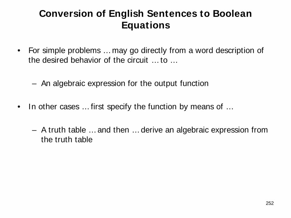
Conversion of English Sentences to Boolean Equations
• For simple problems … may go directly from a word description of the desired behavior of the circuit … to …
– An algebraic expression for the output function
• In other cases … first specify the function by means of …
– A truth table … and then … derive an algebraic expression from the truth table
252
253
Combinational Logic Design Using a
Truth Table
Combinational Logic Design Using a Truth Table
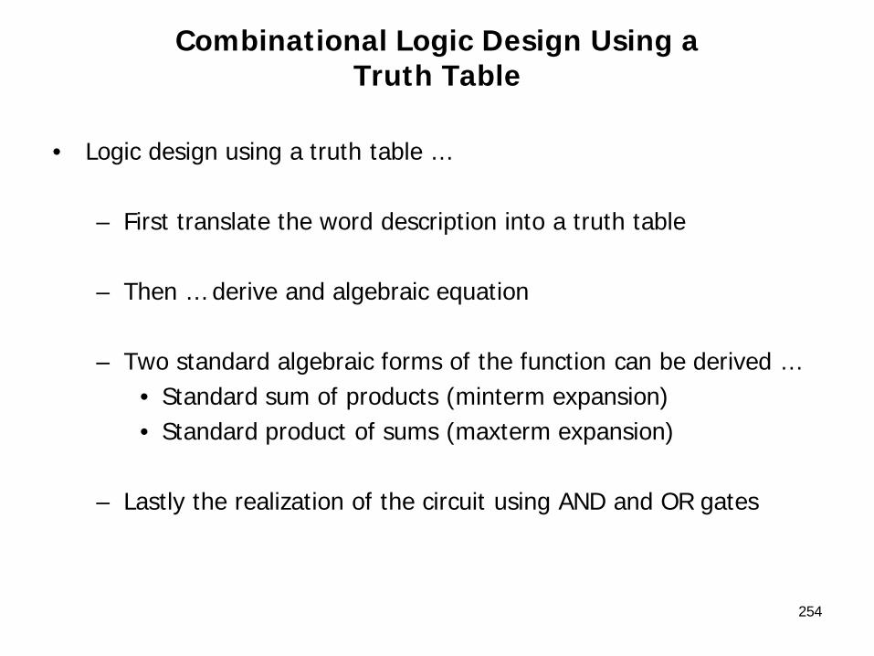
• Logic design using a truth table …
– First translate the word description into a truth table
– Then … derive and algebraic equation
– Two standard algebraic forms of the function can be derived …• Standard sum of products (minterm expansion) • Standard product of sums (maxterm expansion)
– Lastly the realization of the circuit using AND and OR gates
254

255
Minterm and Maxterm Expansions

256
Minterm Expansions

Minterm Expansions
• Each of the terms in the equation from our prior example …
f = A′BC + AB′C′ + AB′C + ABC′ + ABC
• Recall that a literal is a variable or its complement
• Is referred to as a minterm …
– In general … a minterm of n variables is …• A product of n literals in which …
– Each variable appears exactly once in either true or complemented form … but not both
257
Minterm Expansions
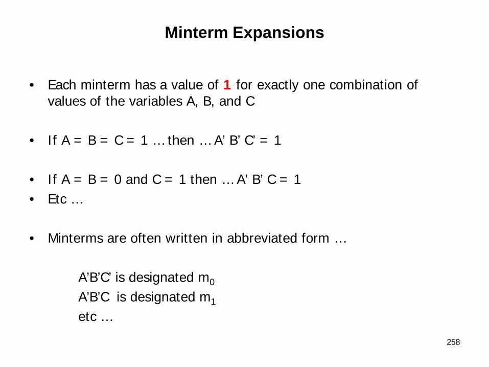
• Each minterm has a value of 1 for exactly one combination of values of the variables A, B, and C
• If A = B = C = 1 … then … A’ B’ C’ = 1
• If A = B = 0 and C = 1 then … A’ B’ C = 1• Etc …
• Minterms are often written in abbreviated form …
A’B’C’ is designated m0
A’B’C is designated m1
etc …
258

Minterm Expansions
• The following Table … lists all of the minterms of the three variables A, B, and C
• In general … the minterm which corresponds to row i of the truth table is designated mi … NOTE … i is usually written in decimal
259
Minterm Expansions
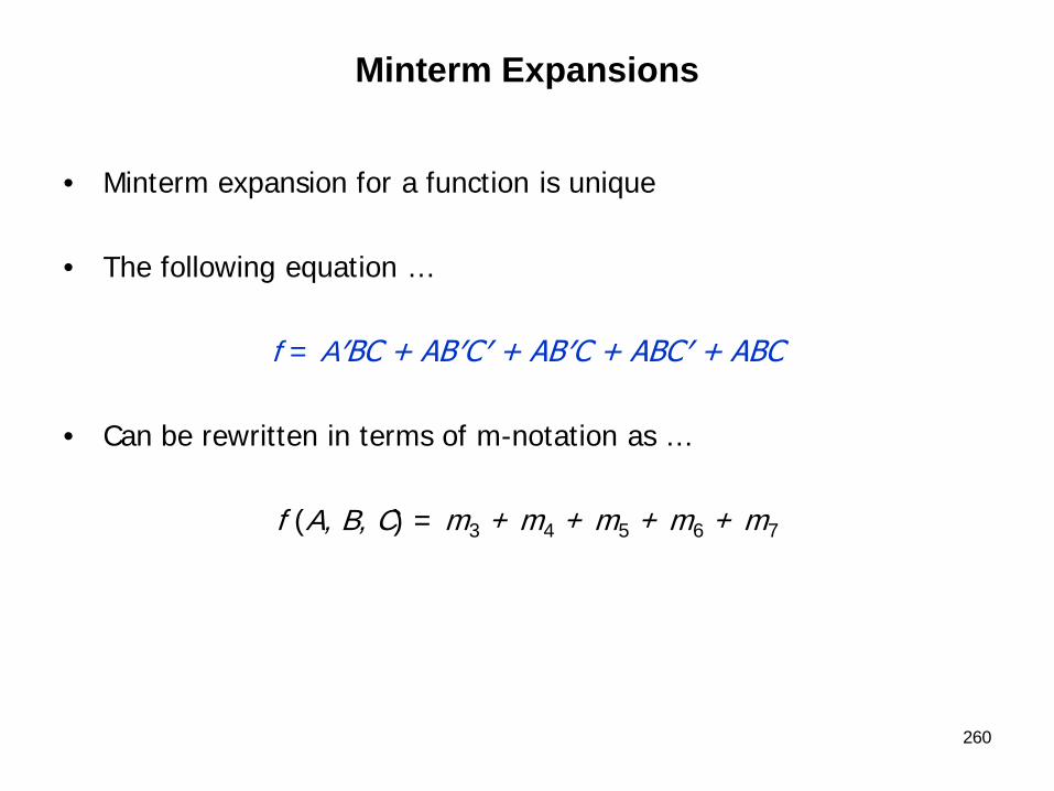
• Minterm expansion for a function is unique
• The following equation …
f = A′BC + AB′C′ + AB′C + ABC′ + ABC
• Can be rewritten in terms of m-notation as …
f (A, B, C) = m3 + m4 + m5 + m6 + m7
260
Minterm Expansions
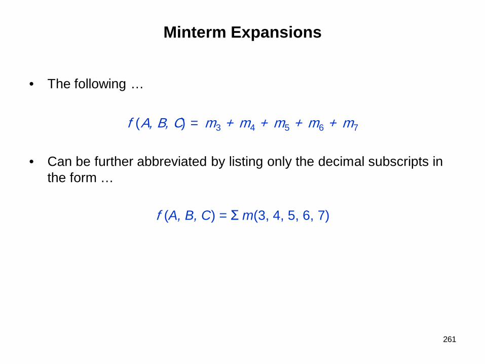
• The following …
f (A, B, C) = m3 + m4 + m5 + m6 + m7
• Can be further abbreviated by listing only the decimal subscripts in the form …
f (A, B, C) = Ʃ m(3, 4, 5, 6, 7)
261

262
Maxterm Expansions

Maxterm Expansions
• Each of the sum terms (factors) in the equation from our prior example …
f = (A + B + C)(A + B + C′)(A + B′ + C)
• Is referred to as a maxterm …
– In general … a maxterm of n variables is …• A sum of n literals in which …
– Each variable appears exactly once in either true or complemented form … but not both
263
Maxterm Expansions
• Each maxterm has a value of 0 for exactly one combination of values of the variables A, B, and C
• If A = B = C = 0 … then … A + B + C = 0
• If A = B = 0 and C = 1 then … A + B + C’ = 0• Etc …
• Maxterms are often written in abbreviated form … Mi
264
Maxterm Expansions
• The following Table … lists all of the maxterms of the three variables A, B, and C
265

Maxterm Expansions
• Maxterm expansion for a function is unique
• The following equation …
f = (A + B + C)(A + B + C′)(A + B′ + C)
• Can be rewritten in terms of M-notation as …
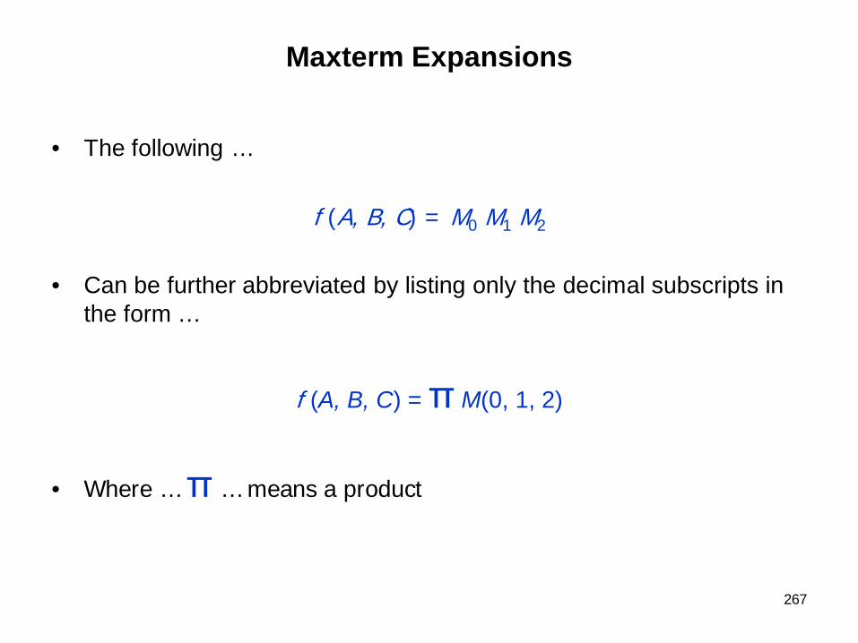
f (A, B, C) = M0 M1 M2
266
Maxterm Expansions
• The following …
f (A, B, C) = M0 M1 M2
• Can be further abbreviated by listing only the decimal subscripts in the form …
f (A, B, C) = π M(0, 1, 2)
• Where … π … means a product
267

268
General
Minterm and Maxterm Expansions

General Minterm and Maxterm Expansions
• Table below summarizes the procedures for conversion between minterm and maxterm expansions of F and F'
269

270
Incompletely Specified Functions
Incompletely Specified Functions
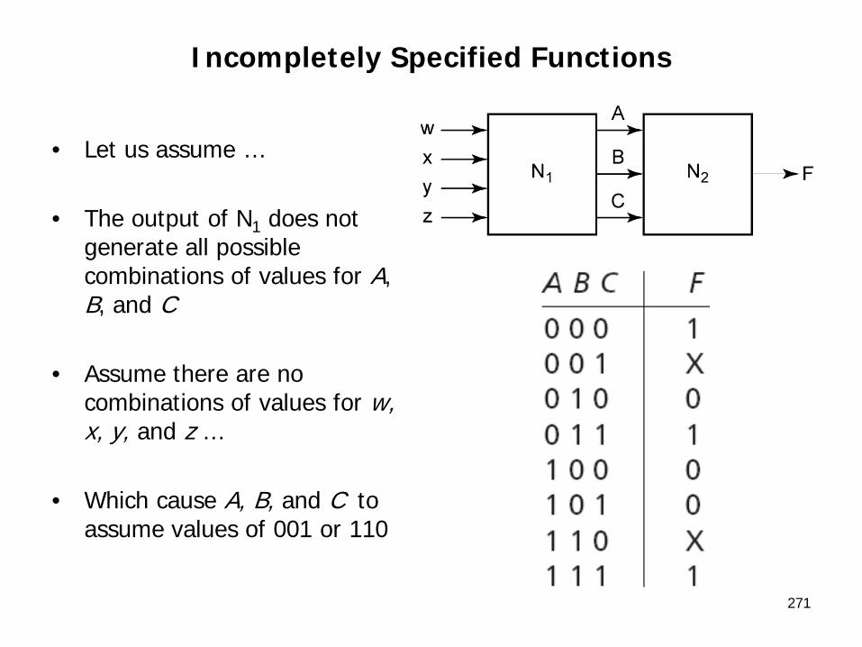
• Let us assume …
• The output of N1 does not generate all possible combinations of values for A, B, and C
• Assume there are no combinations of values for w, x, y, and z …
• Which cause A, B, and C to assume values of 001 or 110
271

Incompletely Specified Functions
• The minterm expansion for the Table is …
• The maxterm expansion for Table is …
272

273
Design of Binary Adders
andSubtractors
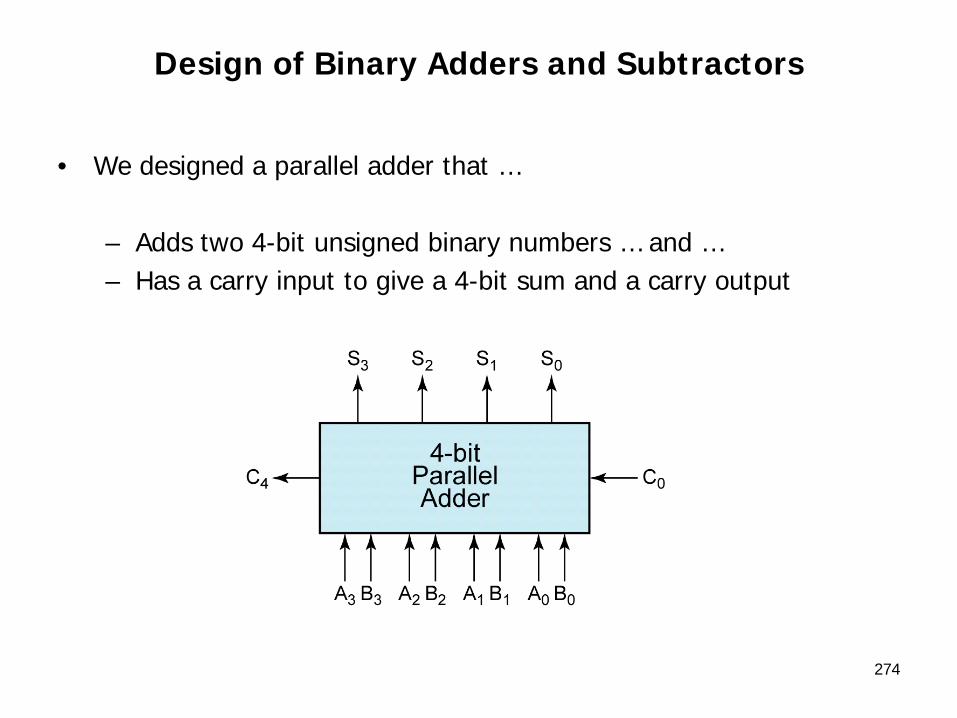
Design of Binary Adders and Subtractors
• We designed a parallel adder that …
– Adds two 4-bit unsigned binary numbers … and … – Has a carry input to give a 4-bit sum and a carry output
274

Design of Binary Adders and Subtractors
275

Design of Binary Adders and Subtractors
• The full adder …
• Truth table output for the full adder can be developed as folllows …
– Each row of the table are found by adding up the input bits … and …
– Splitting the result into a carry out … and … a sum bit
276

Design of Binary Adders and Subtractors
277
X Y Cin Cout Sum 0 0 0 0 0 0 0 1 0 1 0 1 0 0 1 0 1 1 1 0 1 0 0 0 1 1 0 1 1 0 1 1 0 1 0 1 1 1 1 1

278
Chapter 5 …
KARNAUGH MAPS

Karnaugh map (K-map) - Introduction
• Switching functions … can generally be simplified by using …
– Algebraic techniques
• Two problems arise when algebraic procedures are used …
– The procedures are difficult to apply in a systematic way
– It is difficult to tell when you have arrived at a minimum solution
• The Karnaugh map … aka … K-Map method is …
– Generally faster and easier to apply than other simplification methods
279
280
Karnaugh map (K-map) - Introduction
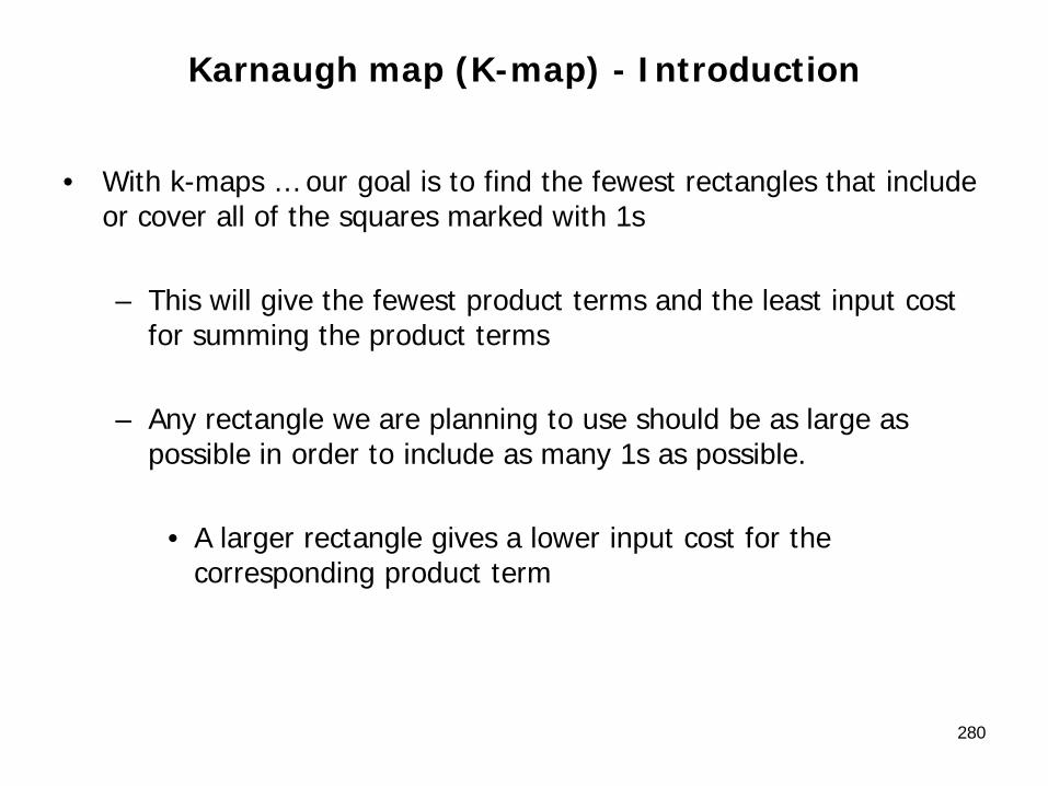
• With k-maps … our goal is to find the fewest rectangles that include or cover all of the squares marked with 1s
– This will give the fewest product terms and the least input cost for summing the product terms
– Any rectangle we are planning to use should be as large as possible in order to include as many 1s as possible.
• A larger rectangle gives a lower input cost for the corresponding product term
281
Two … and … Three Variable K-Maps
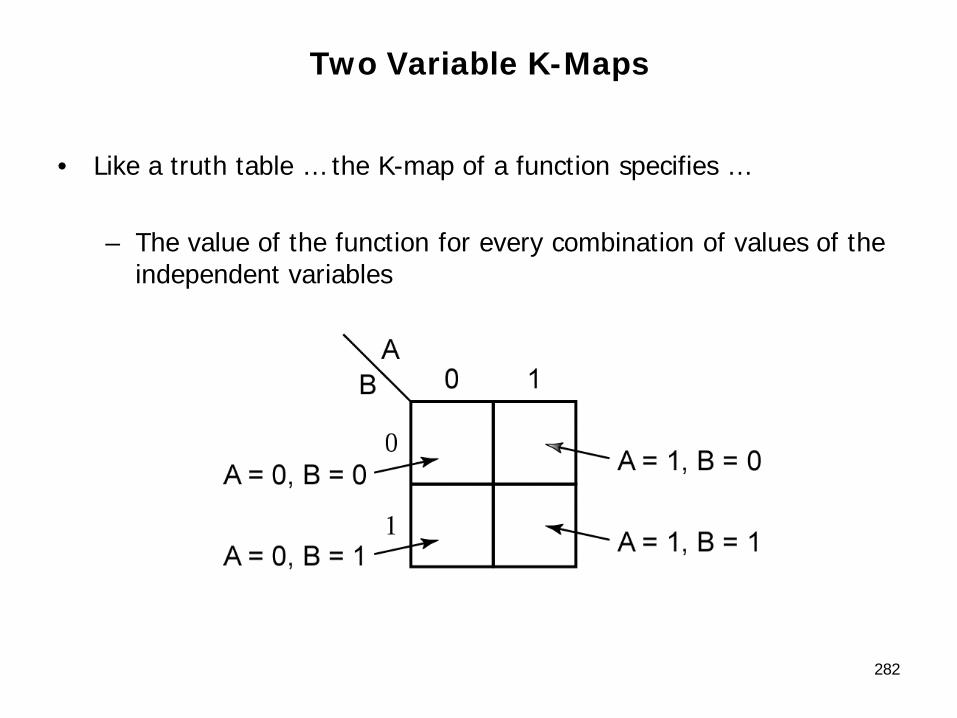
Two Variable K-Maps
• Like a truth table … the K-map of a function specifies …
– The value of the function for every combination of values of the independent variables
282
Two Variable K-Maps
• The truth table for the function … F …
283
Two Variable K-Maps
• Read minterms from the map …
– A “1” in square 00 indicates that A’B’ is a minterm of F
– A “1” in square 01 indicates that A’B is a minterm
284

Two Variable K-Maps
• Minterms in adjacent squares of the map can be combined since they differ in only one variable
• A’B’ and A’B combine to form A’ …
– Indicate by looping the corresponding 1’s on the map
285

286
Three Variable K-Maps
Three Variable K-Maps
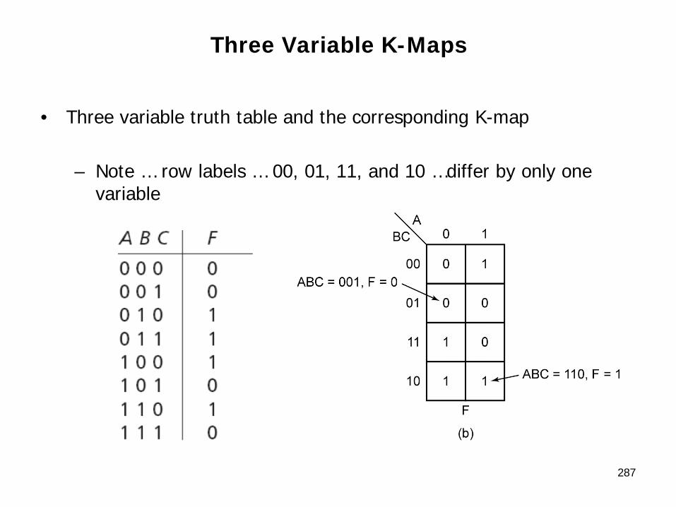
• Three variable truth table and the corresponding K-map
– Note … row labels … 00, 01, 11, and 10 …differ by only one variable
287

Three Variable K-Maps
• Location of Minterms on a Three Variable K-Map …
288

Three Variable K-Maps
• Minterms in adjacent squares of the map differ in only one variable … therefore … can be combined using the theorem XY’ + XY = X
289

Three Variable K-Maps
• K-Map of F (a, b, c) = Σ m(1, 3, 5) = ∏ M(0, 2, 4, 6, 7)
290

291
K-Maps for Product Terms
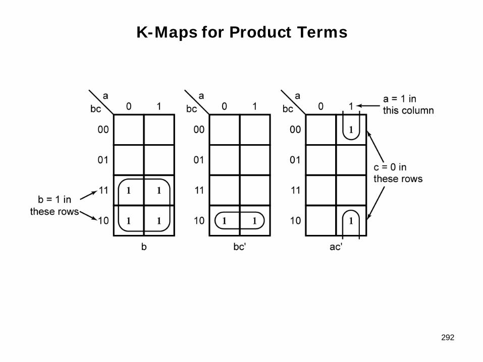
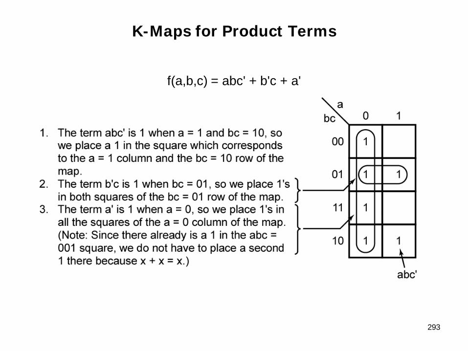
K-Maps for Product Terms
292
K-Maps for Product Terms
f(a,b,c) = abc' + b'c + a'
293
294
Simplification of aThree-Variable Function

Simplification of aThree-Variable Function
295

296
Complement
Complement
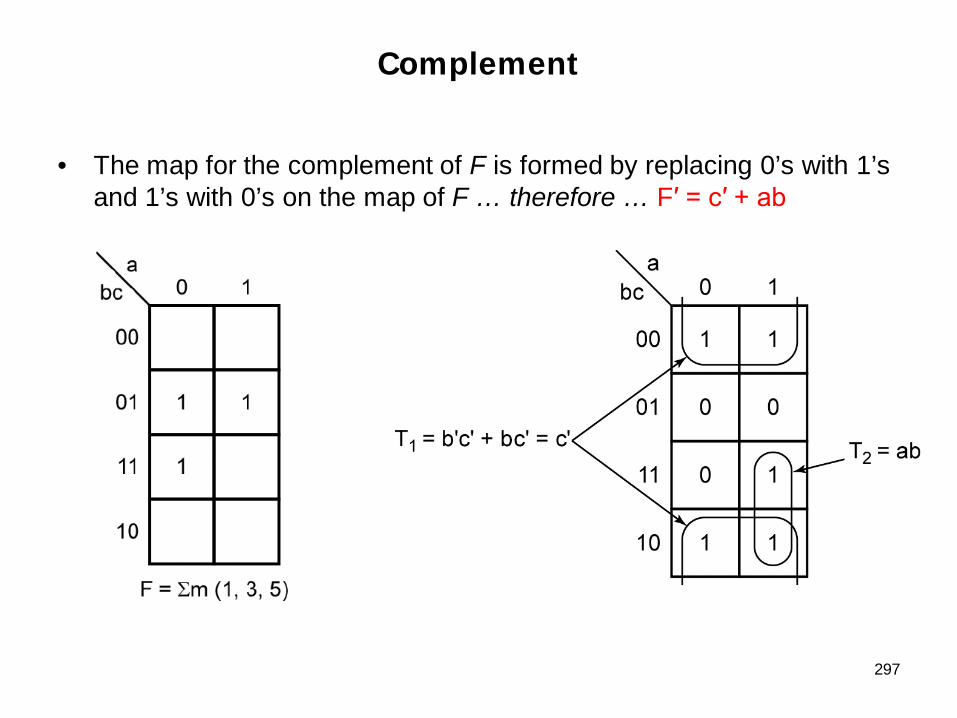
• The map for the complement of F is formed by replacing 0’s with 1’s and 1’s with 0’s on the map of F … therefore … F′ = c′ + ab
297

298
Four-Variable K-Map

Four Variable K-Map
• Each minterm is located adjacent to the four terms … with which it can combine
• For example … m5 (0101) could combine with … m1 (0001) … m4 (0100) … m7 (0111) … or … m13 (1101)
299

300
Simplification of an Incompletely Specified
Function
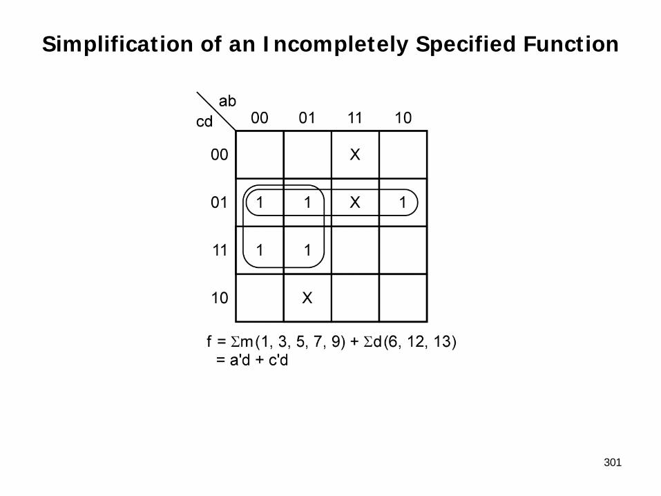
Simplification of an Incompletely Specified Function
301

302
Determination of MinimumExpressions
UsingEssential Prime Implicants

Implicants and Prime Implicants
• Any single 1 … or … any group of 1’s … which …
– Can be combined together on a map of the function F …
• Represents a product term which is called an implicant of F
303
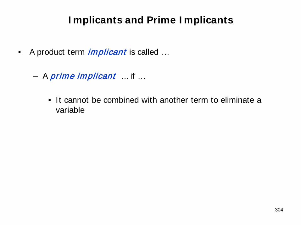
Implicants and Prime Implicants
• A product term implicant is called …
– A prime implicant … if …
• It cannot be combined with another term to eliminate a variable
304
Implicants and Prime Implicants
305
Implicant
Prime Implicant
Prime Implicant
Prime Implicant
Implicant
Implicant

306
Essential Prime Implicants
Essential Prime Implicants
• If a minterm is covered by only one prime implicant …– That prime implicant is said to be essential … and …
– It must be included in the minimum sum of products
307
Essential Prime Implicants
Prime Implicants
Implicants
Essential Prime Implicants
• 1’s shaded in blue are covered by only one prime implicant (essential) …– All other 1’s are covered by at least two prime implicants
308

309
Five Variable K-Maps
Five Variable K-Maps
• A five-variable map can be constructed in three dimensions by placing one four-variable map on top of a second one. Terms in the bottom layer are numbered 0 through 15 and corresponding terms in the top layer are numbered 16 through 31, so that the terms in the bottom layer contain A' and those in the top layer contain A.
• To represent the map in two dimensions, we will divide each square in a four-variable map by a diagonal line and place terms in the bottom layer below the line and terms in the top layer above the line.
310
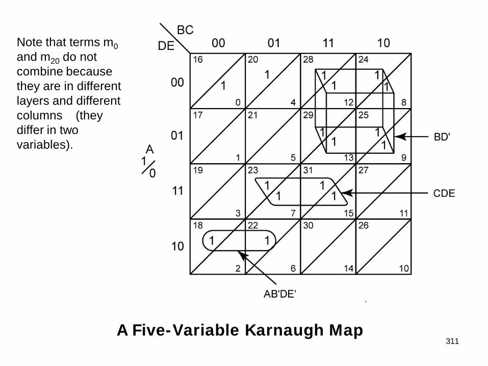
311A Five-Variable Karnaugh Map
Note that terms m0and m20 do not combine because they are in different layers and different columns (they differ in two variables).

312
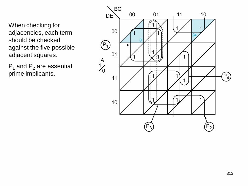
Each term can be adjacent to exactly five other terms: four in the same layer and one in the other layer.
313
When checking for adjacencies, each term should be checked against the five possible adjacent squares.
P1 and P2 are essential prime implicants.

314
Karnaugh map (K-map)
315
Chapter 6 …
Quine-McCluskey Method

Quine-McCluskey Method
• We did not cover this chapter!!!
316

317
Chapter 7 …
MULTI-LEVEL GATE CIRCUITS
NAND AND NOR GATES
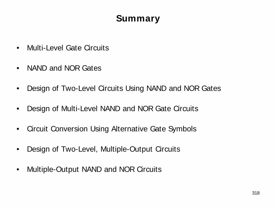
Summary
• Multi-Level Gate Circuits
• NAND and NOR Gates
• Design of Two-Level Circuits Using NAND and NOR Gates
• Design of Multi-Level NAND and NOR Gate Circuits
• Circuit Conversion Using Alternative Gate Symbols
• Design of Two-Level, Multiple-Output Circuits
• Multiple-Output NAND and NOR Circuits
318

319
Multi-Level Gate Circuits

320
Terminology

Terminology
• AND-OR circuit …– A two-level circuit composed of a level of AND gates followed by
an OR gate at the output
• OR-AND circuit …– A two-level circuit composed of a level of OR gates followed by
an AND gate at the output
• OR-AND-OR circuit … – A three-level circuit composed of a level of OR gates followed by
a level of AND gates followed by an OR gate at the output
321

Terminology
• Circuit of AND and OR gates …– Implies no particular ordering of the gates …
• The output gate may be either AND or OR
322

323
Tree Diagrams

Tree Diagrams
• Tree diagram created from a Given expression …– Has … 4 Levels
• Each node on a tree diagram represents a gate …– 6 Gates
• The number of gate inputs is written beside each node … – 13 Inputs
324

Tree Diagrams
• Corresponding circuit for the Four-Level Realization of Z …
325

326
Changing the Number of Levels
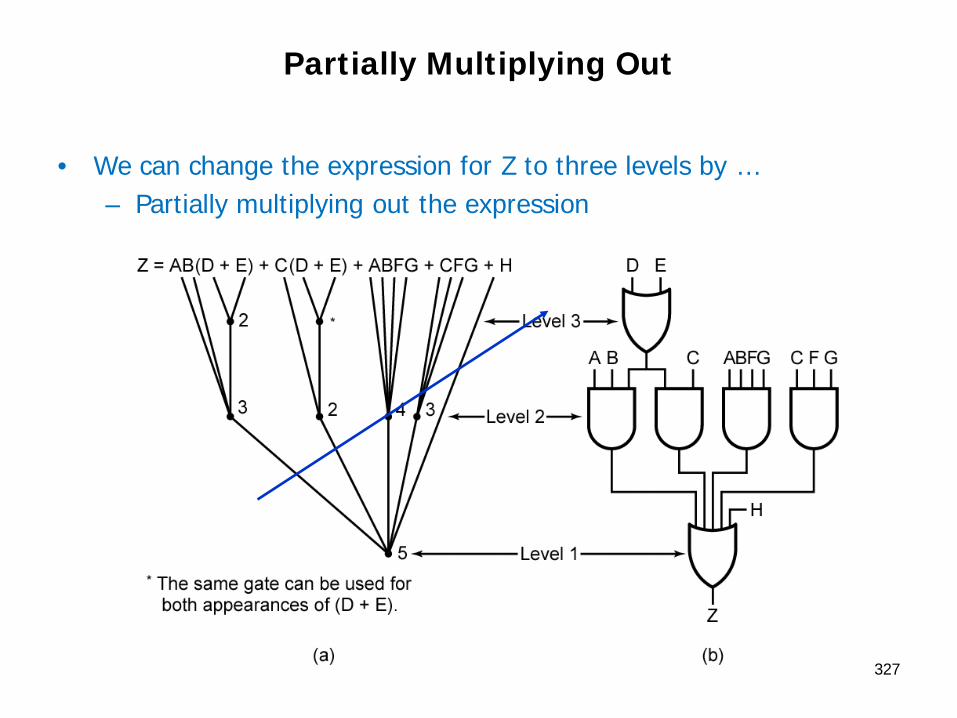
Partially Multiplying Out
• We can change the expression for Z to three levels by … – Partially multiplying out the expression
327
328
To get a Three-Level Circuit …

Three-level circuit with an AND gate output
• To get a three-level circuit with an AND gate output …
– We partially multiply out using … (X + Y)(X + Z) = X + Y Z
329

330
Minimum Solution …

Minimum Solution Determination
• In general … to be sure of obtaining a minimum solution …
– One must find both the circuit with the AND-gate output and the one with the OR-gate output
331

332
NAND and NOR Gates

333
NAND Gates

NAND Gates
• Below … shows a three-input NAND gate
• The small circle (or “bubble”) at the gate output …
– Indicates inversion
334

NAND Gates
• The NAND gate output is …
F = (ABC)′ = A′ + B′ + C′
335

NAND Gates
• An n-input NAND gate is …
336

337
NOR Gates
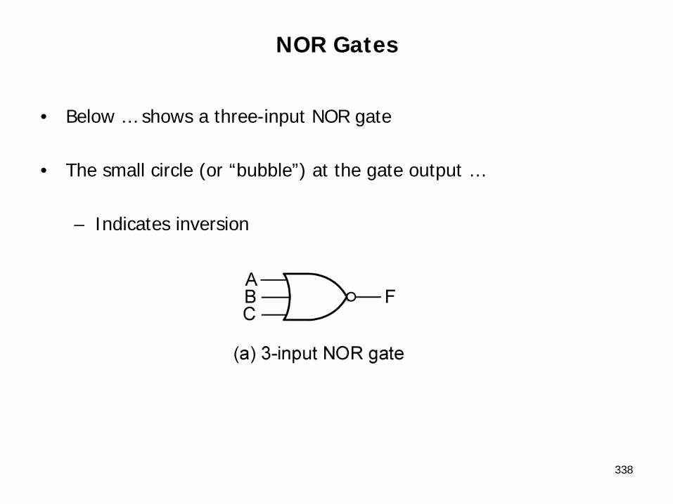
NOR Gates
• Below … shows a three-input NOR gate
• The small circle (or “bubble”) at the gate output …
– Indicates inversion
338

NOR Gates
• Therefore … the NOR gate is equivalent to …
– An OR gate followed by an inverter
• The NOR gate output is …
F = (A + B + C)′ = A′B′C′
339
NOR Gates
• An n-input NOR gate is …
340

341
Functionally Complete Set of Gates
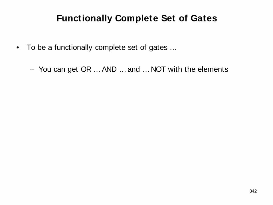
Functionally Complete Set of Gates
• To be a functionally complete set of gates …
– You can get OR … AND … and … NOT with the elements
342
Functionally Complete Set of Gates
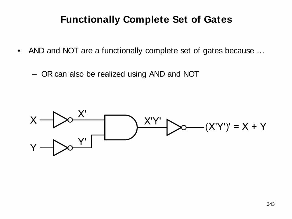
• AND and NOT are a functionally complete set of gates because …
– OR can also be realized using AND and NOT
343
Functionally Complete Set of Gates
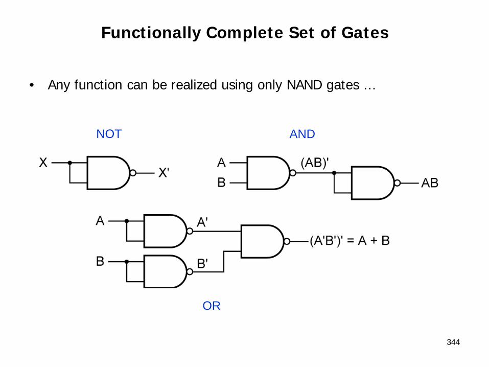
• Any function can be realized using only NAND gates …
344
OR
ANDNOT
345
Design of Two-Level NAND-and NOR-Gate Circuits
346
Design of Two-Level NAND-Gate Circuits
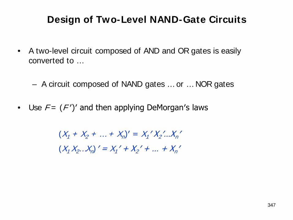
Design of Two-Level NAND-Gate Circuits
• A two-level circuit composed of AND and OR gates is easily converted to …
– A circuit composed of NAND gates … or … NOR gates
• Use F = (F ′)′ and then applying DeMorgan′s laws
(X1 + X2 + … + Xn)′ = X1′ X2′…Xn′
(X1 X2…Xn)′ = X1′ + X2′ + … + Xn′
347

349
Design of Two-Level NOR-Gate Circuits

Design of Two-Level NOR-Gate Circuits
• If we want a two-level circuit containing only NOR gates …
– Start with the minimum product-of-sums form for F instead of the minimum sum-of-products
350

Design of Two-Level NOR-Gate Circuits
• After obtaining the minimum product-of-sums from a K-map …
– F can be written in the following two-level forms again using F = (F ′)′ and then applying DeMorgan′s laws …
F = (A + B + C)(A + B′ + C′)(A + C′ + D) OR-AND
= {[(A + B + C)(A + B′ + C′)(A + C′ + D)]′ }′
= [(A + B + C)′ + (A + B′ + C′)′ + (A + C′ + D)′]′ NOR-NOR
= (A′B′C′ + A′BC + A′CD′)′ AND-NOR
= (A′B′C′)′ • (A′BC)′ • (A′CD′)′ NAND-AND
• The next slide shows the above circuits …
351


353
Design of Minimum Two-Level NAND-NAND Circuits
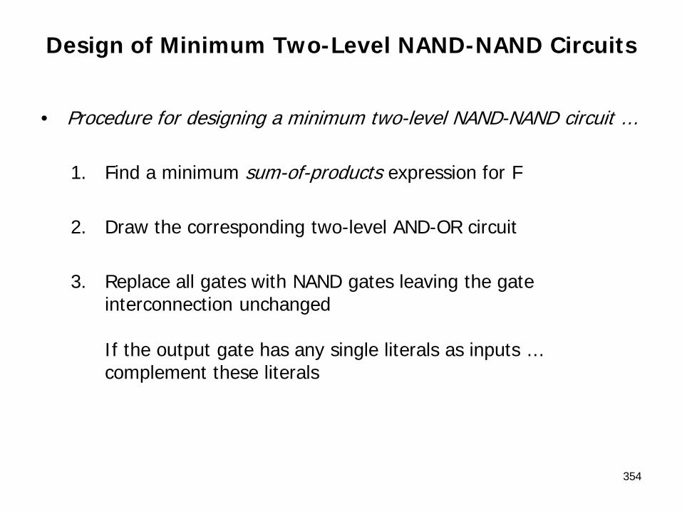
Design of Minimum Two-Level NAND-NAND Circuits
• Procedure for designing a minimum two-level NAND-NAND circuit …
1. Find a minimum sum-of-products expression for F
2. Draw the corresponding two-level AND-OR circuit
3. Replace all gates with NAND gates leaving the gate interconnection unchanged
If the output gate has any single literals as inputs … complement these literals
354

355
Design of Multi-Level NAND-and NOR-Gate Circuits

Design of Multi-Level NAND- and NOR-Gate Circuits
• The following procedure may be used to design multi-level NAND-gate circuits …
1. Simplify the switching function to be realized
2. Design a multi-level circuit of AND and OR gates. The output gate must be OR. AND gate outputs cannot be used as AND-gate inputs; OR-gate outputs cannot be used as OR-gate inputs
3. Number the levels starting with the output gate as level 1. Replace all gates with NAND gates, leaving all interconnections between gates unchanged, leave the inputs to levels 2,4,6,… unchanged. Invert any literals which appear as inputs to levels 1,3,5,…
356
357
Alternative Gate Symbols
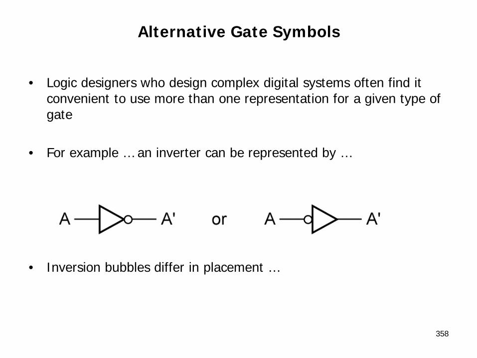
Alternative Gate Symbols
• Logic designers who design complex digital systems often find it convenient to use more than one representation for a given type of gate
• For example … an inverter can be represented by …
• Inversion bubbles differ in placement …
358

Alternative Gate Symbols
• Equivalent gate symbols based on DeMorgan′s Laws
359

Alternate Symbols
• Can use alternate symbols to facilitate analysis and design of NAND and NOR gate circuits
360

361
Design of Two-Level, Multiple-Output Circuits
Design of Two-Level, Multiple-Output Circuits
• Solution of digital design problems often requires the realization of several functions of the same variables
• Although each function could be realized separately …
– The use of some gates in common between two or more functions sometimes leads to a more economical realization
362

363
Multiple-Output NAND- and NOR-Gate Circuits

Multiple-Output NAND- and NOR-Gate Circuits
• The procedure for … single-output … multi-level NAND- and NOR-gate circuits …
– Also applies to multiple-output circuits
• If all outputs are OR gates …
– Direct conversion to a NAND-gate circuit is possible
• If all outputs are AND gates …
– Direct conversion to a NOR-gate circuit is possible
364
365
Chapter 8 …
COMBINATIONAL CIRCUIT DESIGN AND SIMULATION
USING GATES

Overview
• Review of Combinational Circuit Design
• Design Circuits with Limited Gate Fan-In
• Gate Delays and Timing Diagrams
• Hazards in Combinational Logic
• Simulation and Testing of Logic Circuits
366
367
Design of Circuits with Limited Gate Fan-In
Design of Circuits with Limited Gate Fan-In
• Fan-in …
– The maximum number of inputs on each gate
• In practical logic design problems …
– The maximum number of inputs on each gate is limited
368
Design of Circuits with Limited Gate Fan-In
• If a two-level realization of a circuit requires more gate inputs than allowed …
– Factoring the logic expression to obtain a multi-level realization is necessary
369
370
Multiple Output Circuits …

Design of Multiple-Output Circuits
• Previous techniques for designing two-level … multiple-output circuits …
– Are not very effective for designing multiple-output circuits with more than two levels
• When two-level expressions had common terms …
– Most of these common terms would be lost when the expressions were factored
371
Design of Multiple-Output Circuits
• When designing multiple-output circuits … with more than two levels …
– It is usually best to minimize each function separately
• The resulting two-level expressions must then be factored to increase the number of levels
– Factoring should be done in such a way as to introduce common terms wherever possible
372
373
Gate Delays and Timing Diagrams

374
Gate Delays …

Gate Delays
• When the input to a logic gate is changed …
– The output will not change instantaneously
• The transistors or other switching elements within the gate take a finite time to react to a change in input … so that …
– The change in the gate output is delayed with respect to the input change
375

Propagation Delay in an Inverter
• Below shows possible input and output waveforms for an inverter
376

377
Timing Diagrams …

Timing Diagrams
• Timing diagrams are frequently used in the analysis of sequential circuits
• They show various signals in the circuit as a function of time
• Several variables are plotted with the same time scale … so that …
– The times at which these variables change with respect to each other can easily be observed
378
Timing Diagrams
• Below shows the timing diagram for a circuit with two gates …
379
380
Hazards in Combinational Logic

Hazards in Combinational Logic
• When the input to a combinational circuit changes …
– Unwanted switching transients may appear in the output
• These transients occur when …
– Different paths from input to output have different propagation delays
381
Hazards in Combinational Logic
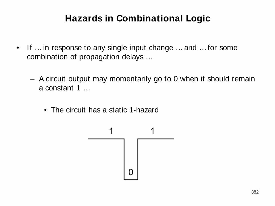
• If … in response to any single input change … and … for some combination of propagation delays …
– A circuit output may momentarily go to 0 when it should remain a constant 1 …
• The circuit has a static 1-hazard
382
Hazards in Combinational Logic
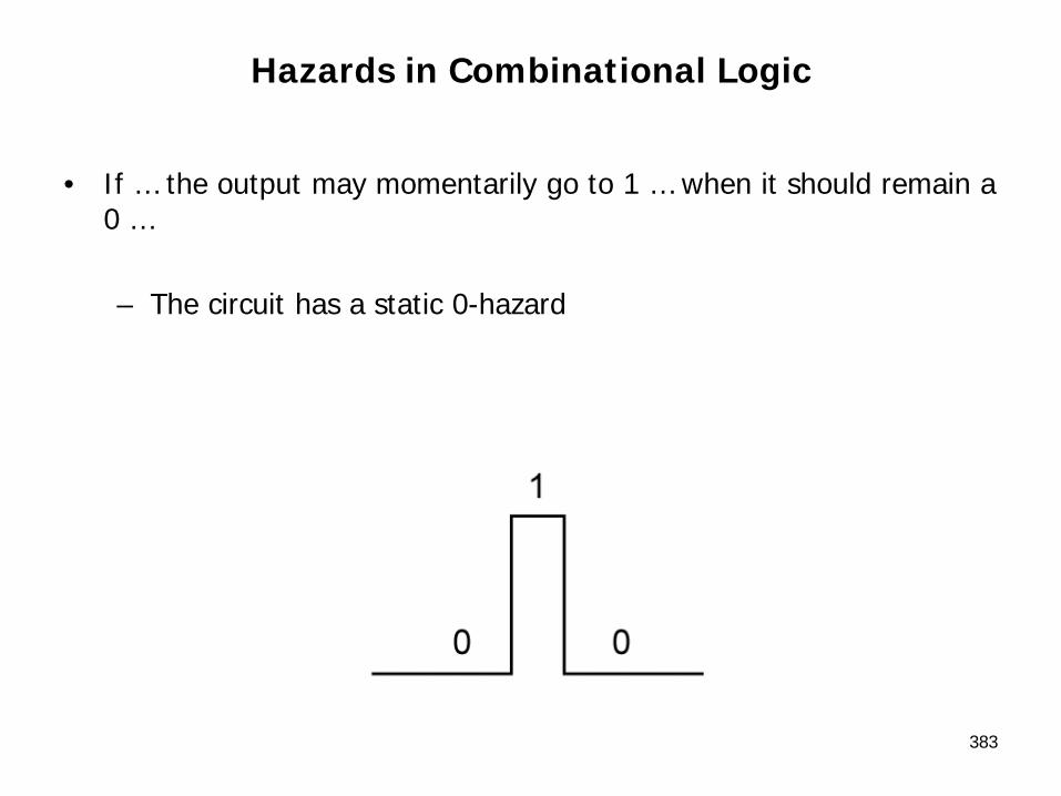
• If … the output may momentarily go to 1 … when it should remain a 0 …
– The circuit has a static 0-hazard
383
Hazards in Combinational Logic
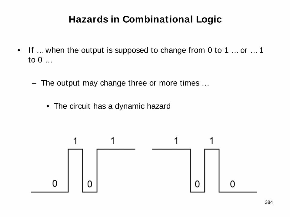
• If … when the output is supposed to change from 0 to 1 … or … 1 to 0 …
– The output may change three or more times …
• The circuit has a dynamic hazard
384
Hazards in Combinational Logic
• In each case the steady-state output of the circuit is correct …
– But … a switching transient appears at the circuit output when the input is changed
385

386
Detecting Hazards …
Detecting Hazards
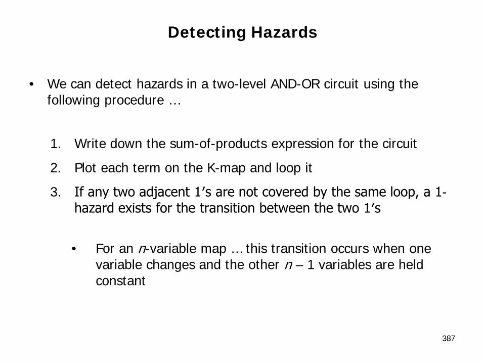
• We can detect hazards in a two-level AND-OR circuit using the following procedure …
1. Write down the sum-of-products expression for the circuit
2. Plot each term on the K-map and loop it
3. If any two adjacent 1′s are not covered by the same loop, a 1-hazard exists for the transition between the two 1′s
• For an n-variable map … this transition occurs when one variable changes and the other n – 1 variables are held constant
387
Detecting Hazards
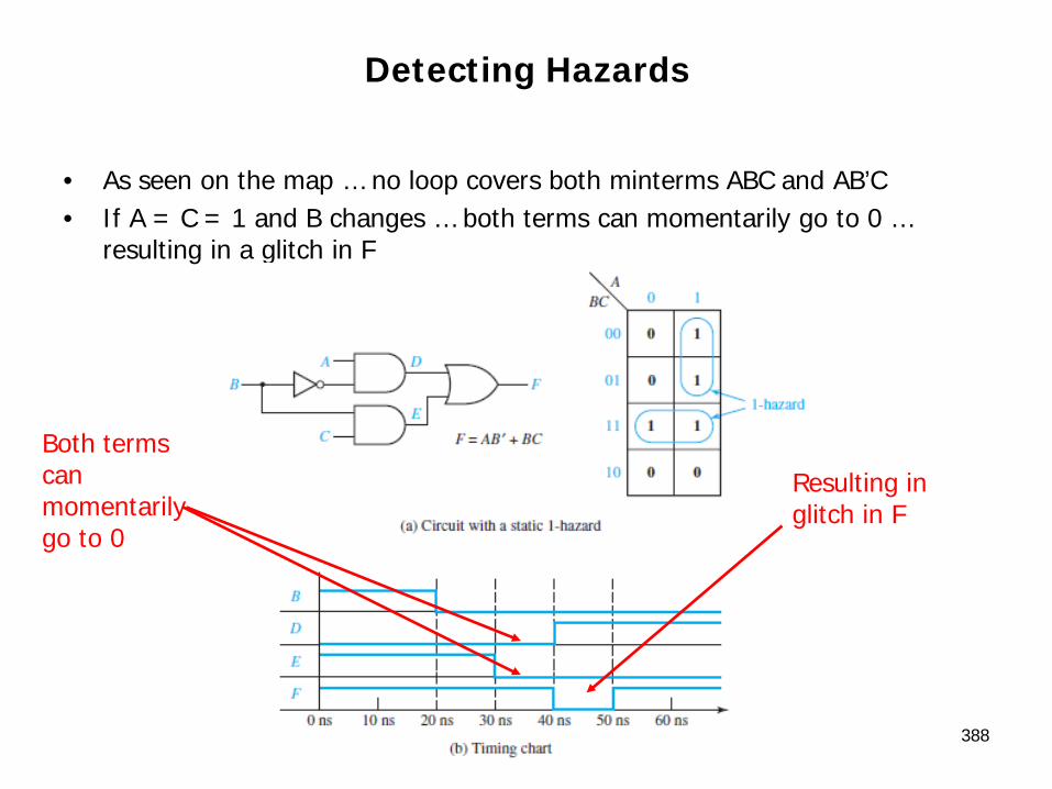
• As seen on the map … no loop covers both minterms ABC and AB’C• If A = C = 1 and B changes … both terms can momentarily go to 0 …
resulting in a glitch in F
388
Both terms can momentarily go to 0
Resulting in glitch in F
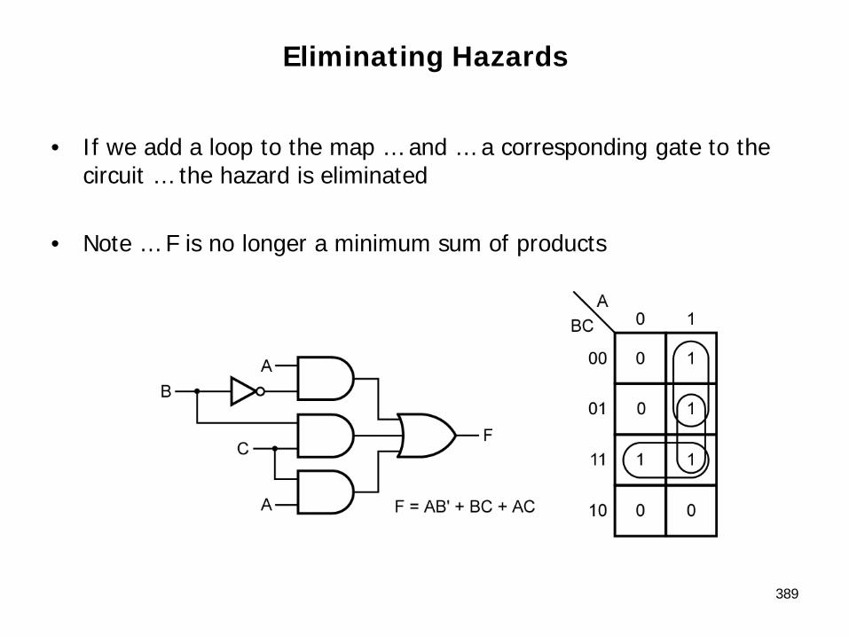
Eliminating Hazards
• If we add a loop to the map … and … a corresponding gate to the circuit … the hazard is eliminated
• Note … F is no longer a minimum sum of products
389

390
Designing a Circuit Free of Hazards …
Designing a Circuit Free of Hazards
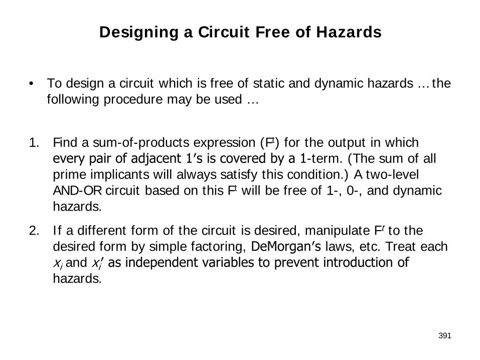
• To design a circuit which is free of static and dynamic hazards … the following procedure may be used …
1. Find a sum-of-products expression (Ft) for the output in which every pair of adjacent 1′s is covered by a 1-term. (The sum of all prime implicants will always satisfy this condition.) A two-level AND-OR circuit based on this Ft will be free of 1-, 0-, and dynamic hazards.
2. If a different form of the circuit is desired, manipulate Ft to the desired form by simple factoring, DeMorgan′s laws, etc. Treat each xi and xi′ as independent variables to prevent introduction of hazards.
391
392
Simulation and Testing of Logic Circuits …
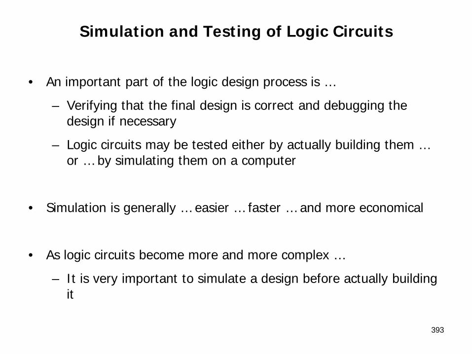
Simulation and Testing of Logic Circuits
• An important part of the logic design process is …
– Verifying that the final design is correct and debugging the design if necessary
– Logic circuits may be tested either by actually building them … or … by simulating them on a computer
• Simulation is generally … easier … faster … and more economical
• As logic circuits become more and more complex …
– It is very important to simulate a design before actually building it
393
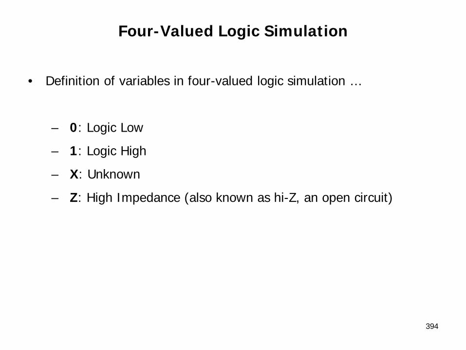
Four-Valued Logic Simulation
• Definition of variables in four-valued logic simulation …
– 0: Logic Low
– 1: Logic High
– X: Unknown
– Z: High Impedance (also known as hi-Z, an open circuit)
394
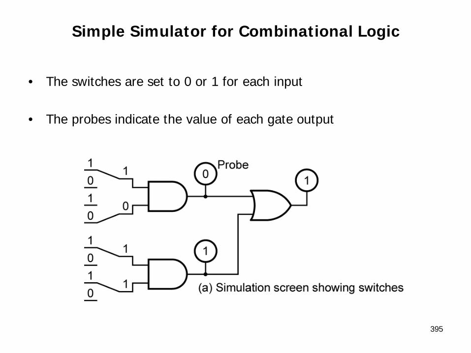
Simple Simulator for Combinational Logic
• The switches are set to 0 or 1 for each input
• The probes indicate the value of each gate output
395
Simple Simulator for Combinational Logic
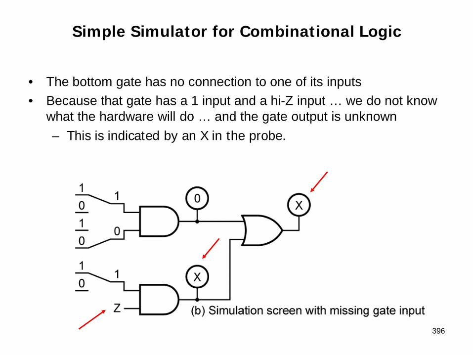
• The bottom gate has no connection to one of its inputs• Because that gate has a 1 input and a hi-Z input … we do not know
what the hardware will do … and the gate output is unknown– This is indicated by an X in the probe.
396
397
Chapter 9 …
MULTIPLEXERS, DECODERS, AND PROGRAMMABLE LOGIC
DEVICES

398
Multiplexers

Multiplexers
• A multiplexer has …
– A group of data inputs … and …
– A group of control inputs
• Used to select one of the data inputs and connect it to the output terminal
• A multiplexer … AKA … MUX …
– Acts like a switch that selects one input
399

2-to-1 Multiplexer and Switch Analog
400
Z = A′I0 + AI1
Data Inputs
Data Controls

Multiplexers
• 8 to 1 MUX needs 3 control inputs to select one data input …• 8 to 1 MUX output equation …Z = A′B′C′I0 + A′B′CI1 + A′BC′I2 + A′BCI3 + AB′C′I4 + AB′CI5 + ABC′I6 + ABCI7
Values for A ... B … and C …
are a binary count!
401
Multiplexers
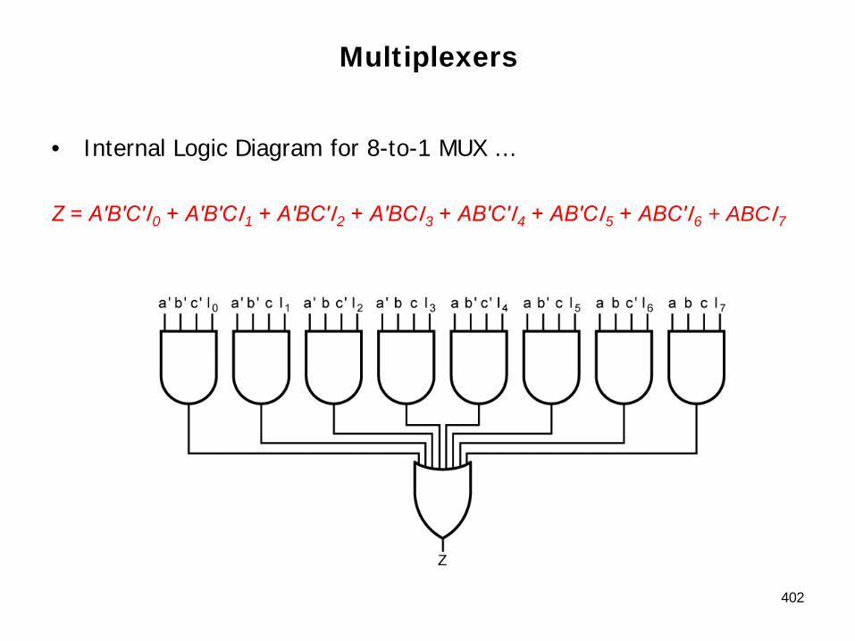
• Internal Logic Diagram for 8-to-1 MUX …
Z = A′B′C′I0 + A′B′CI1 + A′BC′I2 + A′BCI3 + AB′C′I4 + AB′CI5 + ABC′I6 + ABCI7
402

Multiplexers
• Multiplexers are frequently used in digital system design to select the data which is to be processed or stored
403

Quad Multiplexer with Bus Inputs and Output
• The quad MUX … is redrawn … using …
– Bus inputs X and Y … and … bus output Z• The X bus represents the four signals x0 … x1 … x2 … and …
x3 …and … similarly for the Y and Z buses (4 signals)
404

405
Three-State Buffers

406
Buffers

Buffers
• A gate output can only be connected to a limited number of other device inputs with-out degrading the performance of a digital system
• A buffer may be used to increase the driving capability of a gate output
• Buffers are non-inverting …
– Logic value in … is the same as the logic value out
407
Buffer
• Gate Circuit with Added Buffer …
408
F = C

409
Three-State Buffers

Three-State Buffers
• A logic circuit will not operate correctly if the outputs of two or more gates or other logic devices are directly connected to each other
• Example … if one gate has a 0 output (a low voltage) … and … another has a 1 output (a high voltage) …
– When the gate outputs are connected together the resulting output voltage may be some intermediate value that does not clearly represent either a 0 or a 1
410
Three-State Buffers
• Use of three-state logic permits the outputs of two or more gates or other logic devices to be connected together
• The following is a three-state buffer and its logical equivalent
– Three-state buffers are also called tri-state buffers
411

Three-State Buffers
• When …– The enable input B is 1 … the output C equals A– When B is 0 … the output C acts like an open circuit
• Output C is disconnected from the buffer output so that no current can flow
412
Three-State Buffers
• When …• The output C is disconnected from the buffer …
– It is a Hi- Z (high- impedance) state of the output because the circuit offers a very high resistance or impedance to the flow of current
413

414
Multiple Source Selection
Multiple Source Selection
• A multiplexer may be used to select one of several sources to drive a device input
• As an example … if an adder input must come from four different sources …
– A 4-to-1 MUX may be used to select one of the four sources
415

Multiple Source Selection
• Below is a three-state bus …
• 4-Bit Adder with Four Sources for One Operand
– It uses three-state buffers to select one of the sources
416
417
Bi-DirectionalInput / Output Pin
Bi-Directional Input/Output Pin
• Integrated circuits are often designed using bi-directional pins for input and output
– A microcontroller is an example with bi-directional pins
• Bi-directional means … the same pin can be used as an input pin … and …
– As an output pin … but … not both at the same time
418
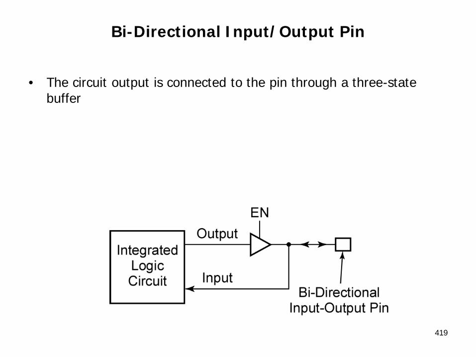
Bi-Directional Input/Output Pin
• The circuit output is connected to the pin through a three-state buffer
419

420
Decoders and Encoders

421
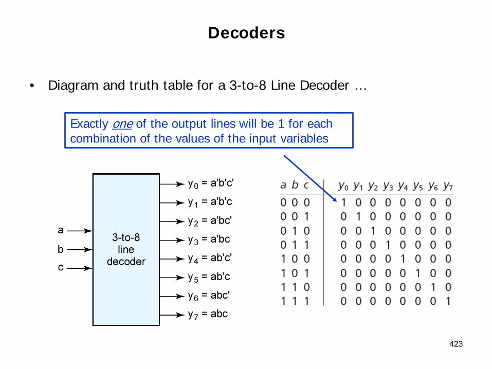
Decoders

Decoders
• The decoder is another commonly used type of integrated circuit
• The decoder generates …
– All of the minterms of the three input variables
• Exactly one of the output lines will be 1 for each combination of the values of the input variables
422
Decoders
• Diagram and truth table for a 3-to-8 Line Decoder …
423
Exactly one of the output lines will be 1 for each combination of the values of the input variables

424
Encoders
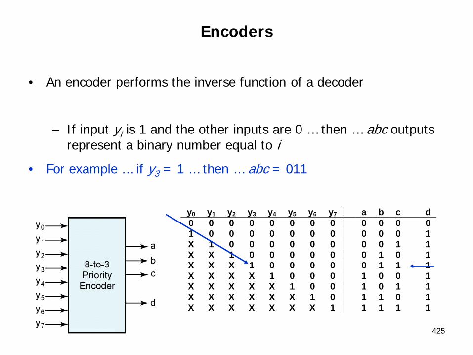
Encoders
• An encoder performs the inverse function of a decoder
– If input yi is 1 and the other inputs are 0 … then … abc outputs represent a binary number equal to i
• For example … if y3 = 1 … then … abc = 011
425
y0 y1 y2 y3 y4 y5 y6 y7 a b c d 0 0 0 0 0 0 0 0 0 0 0 0 1 0 0 0 0 0 0 0 0 0 0 1 X 1 0 0 0 0 0 0 0 0 1 1 X X 1 0 0 0 0 0 0 1 0 1 X X X 1 0 0 0 0 0 1 1 1 X X X X 1 0 0 0 1 0 0 1 X X X X X 1 0 0 1 0 1 1 X X X X X X 1 0 1 1 0 1 X X X X X X X 1 1 1 1 1
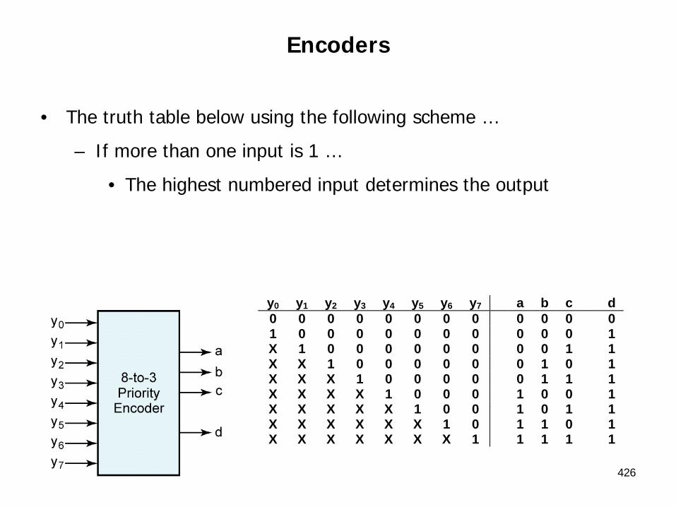
Encoders
• The truth table below using the following scheme …
– If more than one input is 1 …
• The highest numbered input determines the output
426
y0 y1 y2 y3 y4 y5 y6 y7 a b c d 0 0 0 0 0 0 0 0 0 0 0 0 1 0 0 0 0 0 0 0 0 0 0 1 X 1 0 0 0 0 0 0 0 0 1 1 X X 1 0 0 0 0 0 0 1 0 1 X X X 1 0 0 0 0 0 1 1 1 X X X X 1 0 0 0 1 0 0 1 X X X X X 1 0 0 1 0 1 1 X X X X X X 1 0 1 1 0 1 X X X X X X X 1 1 1 1 1

427
Programmable Logic Devices (PLDs)
428
Programmable Logic Devices ( PLDs)
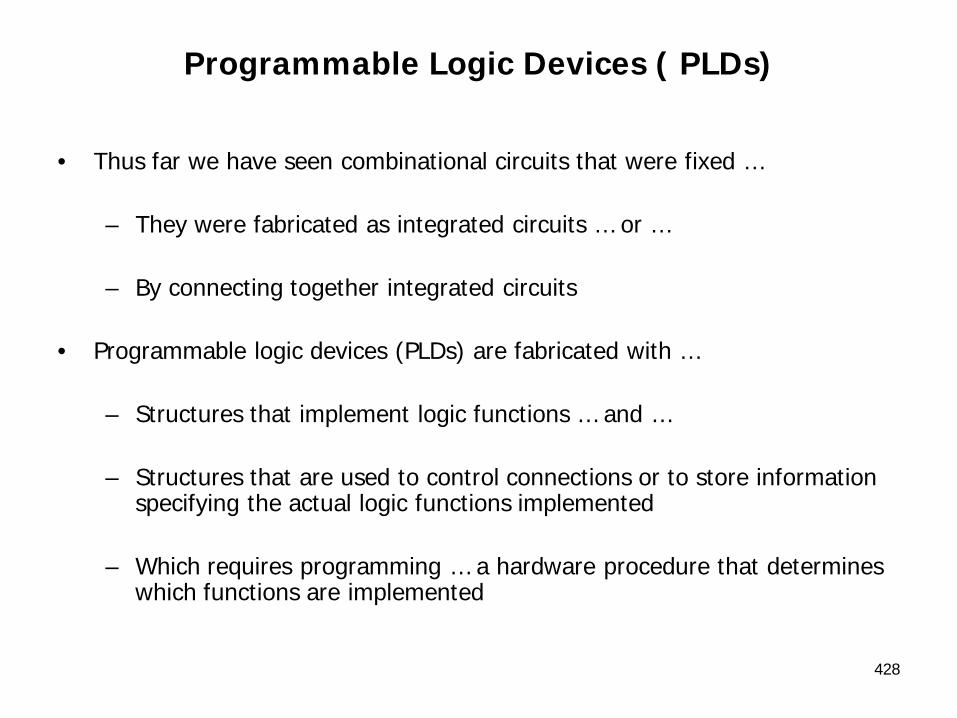
• Thus far we have seen combinational circuits that were fixed …
– They were fabricated as integrated circuits … or …
– By connecting together integrated circuits
• Programmable logic devices (PLDs) are fabricated with …
– Structures that implement logic functions … and …
– Structures that are used to control connections or to store information specifying the actual logic functions implemented
– Which requires programming … a hardware procedure that determines which functions are implemented

429
Programmable Logic Devices ( PLDs)
• Basic programmable logic devices …
– The read- only memory (ROM)
– The programmable logic array (PLA) …and …
– The programmable array logic (PAL) device
– Complex Programmable Logic Devices (CPLD)
– Field-Programmable Gate Arrays (FPGA)
430
Programmable Logic Devices ( PLDs)
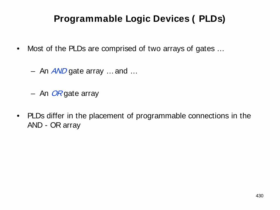
• Most of the PLDs are comprised of two arrays of gates …
– An AND gate array … and …
– An OR gate array
• PLDs differ in the placement of programmable connections in the AND - OR array

431
Notations …
432
Connections
• There are two types of connections between two perpendicular lines …
– Programmable … and …
– Non-programmable
• Also known as a hard-wired connection
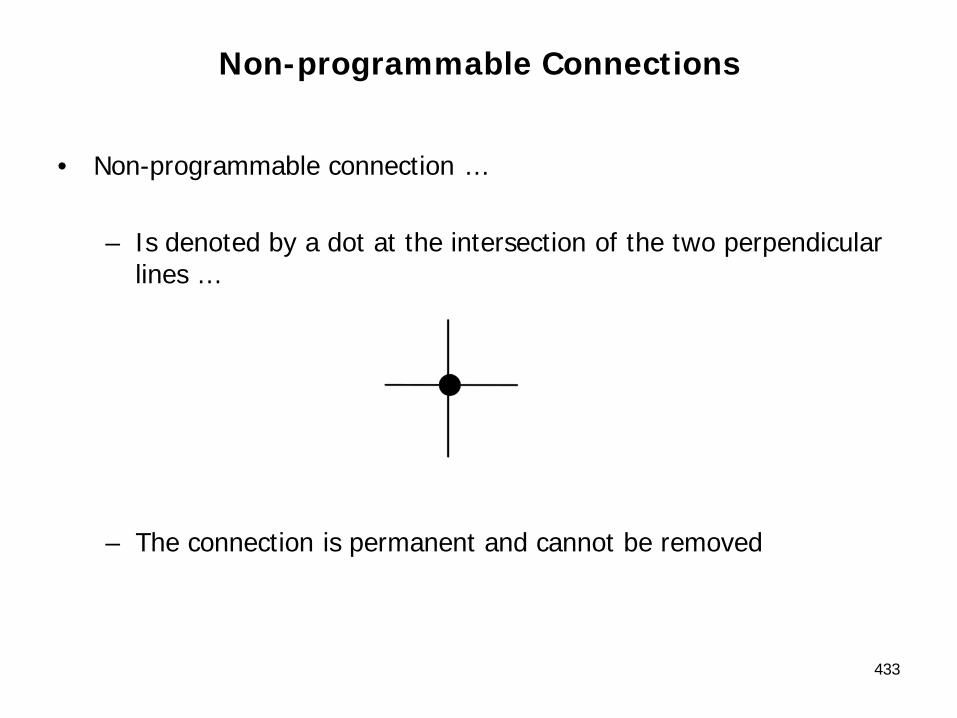
433
Non-programmable Connections
• Non-programmable connection …
– Is denoted by a dot at the intersection of the two perpendicular lines …
– The connection is permanent and cannot be removed

434
Programmable Connections
• Programmable connection …
– A switching element is used to connect two lines …
• Which is shown by an “X” at the intersection of the two lines
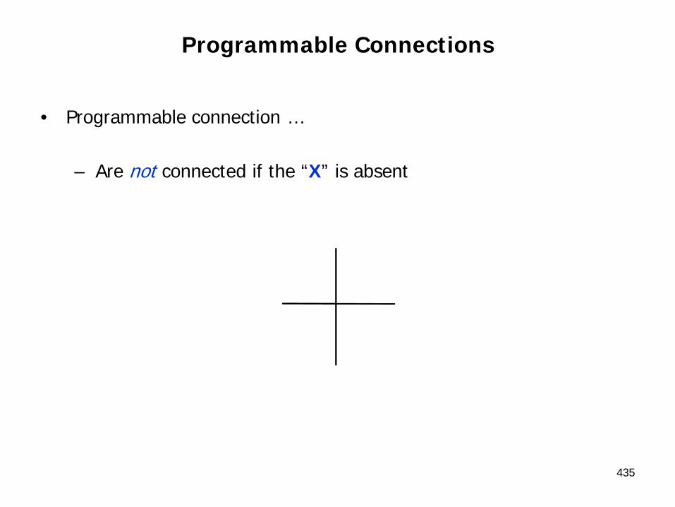
435
Programmable Connections
• Programmable connection …
– Are not connected if the “X” is absent

436
Phase Splitter
• A Phase Splitter is used to generate …
– The TRUE form … and …
– The COMPLEMENTED form of an input

437
Programmable Gates
• For an n-input programmable gate …
– Only one line is drawn and connected to the gate
– A gate can be disconnected by removing the ”X”

438
Read-Only Memories(ROM)
Read-Only Memories
• A read-only memory (ROM) consists of …
– An array of semiconductor devices that are interconnected to store an array of binary data
• Once binary data is stored in the ROM … it can be read out whenever desired … but …
– The data that is stored cannot be changed under normal operating conditions
439

Read-Only Memories
• Below is a ROM which has three input lines and four output lines along with it’s truth table
• The truth table relates the ROM inputs and outputs• For each combination of input values on the three input lines, the
corresponding pattern of 0’ s and 1’ s appears on the ROM output lines.
440

Read-Only Memories
• For each combination of input values on the three input lines … the corresponding pattern of 0’ s and 1’ s appears on the ROM output
• If the combination ABC = 010 is applied to the input lines … the pattern F0F1F2F3 = 0111 appears on the output lines
441
Read-Only Memories
• Each of the output patterns that is stored in the ROM is called a word
• Because the ROM has three input lines … we have 23 eight different combinations of input values– Each input combination serves as an address which can select
one of the eight words stored in the memory
442

Read-Only Memories
• For the ROM below … there are four output lines … therefore …
– Each word is four bits long … and …
• The size of this ROM is 8 words x 4 bits
443
Read-Only Memories
• The input lines serve as an address to select one of the 2n words
• When an input combination is applied to the ROM … the pattern of 0’ s and 1’ s … which is stored in the corresponding word in the memory … appears at the output lines
444

445
Read-Only Memories
• Basic ROM structure …
InputsFixed
AND array(decoder)
ProgrammableOR array OutputsProgrammable
Connections
446
Read-Only Memories
• Depending on the programming technology and approaches … read-only memories have different names …
– ROM … mask programmed
– PROM … fuse or anti-fuse programmed
– EPROM … erasable floating gate programmed
– EEPROM or E2PROM … electrically erasable floating gate programmed
– FLASH Memory … electrically erasable floating gate with multiple erasure and programming modes

447
Chapter 9 …
MULTIPLEXERS, DECODERS, AND PROGRAMMABLE LOGIC
DEVICES

448
Programmable Logic Devices
Programmable Logic Devices
• A programmable logic device … or … PLD …
– A general name for a digital integrated circuit capable of being programmed to provide a variety of different logic functions
449
Programmable Logic Devices
• For digital system is designed using a PLD …
– Changes in the design can easily be made by …
• Changing the programming of the PLD …
– Without having to change the wiring in the system
450

451
Programmable Logic Arrays

Programmable Logic Arrays
• Programmable logic array … PLA
• Performs the same basic function as a ROM
452

Programmable Logic Arrays
• A PLA with n inputs and m outputs can realize m functions of nvariables
453
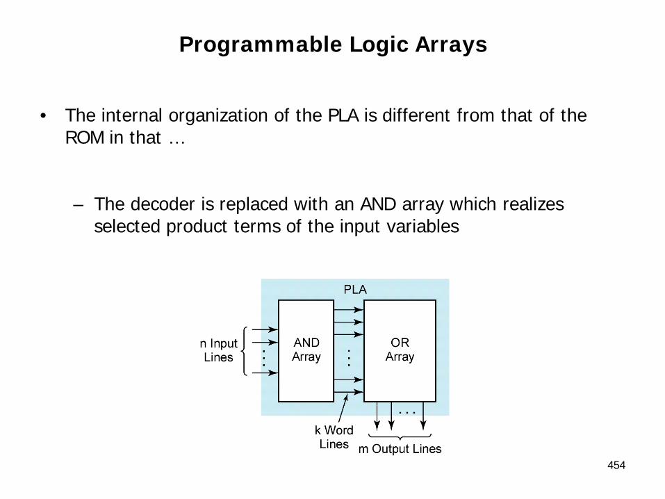
Programmable Logic Arrays
• The internal organization of the PLA is different from that of the ROM in that …
– The decoder is replaced with an AND array which realizes selected product terms of the input variables
454
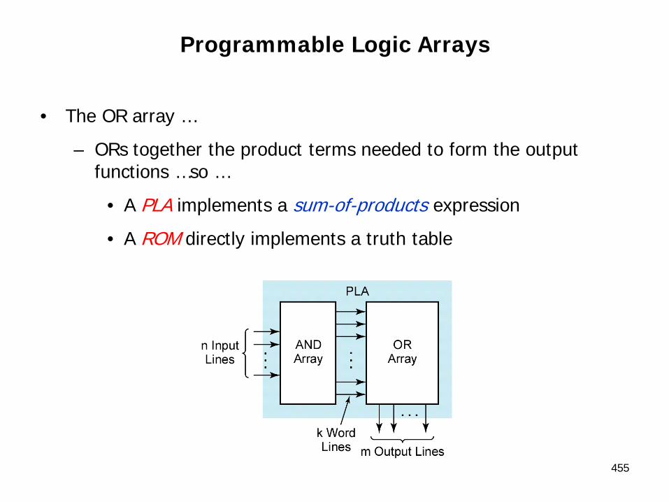
Programmable Logic Arrays
• The OR array …
– ORs together the product terms needed to form the output functions …so …
• A PLA implements a sum-of-products expression
• A ROM directly implements a truth table
455
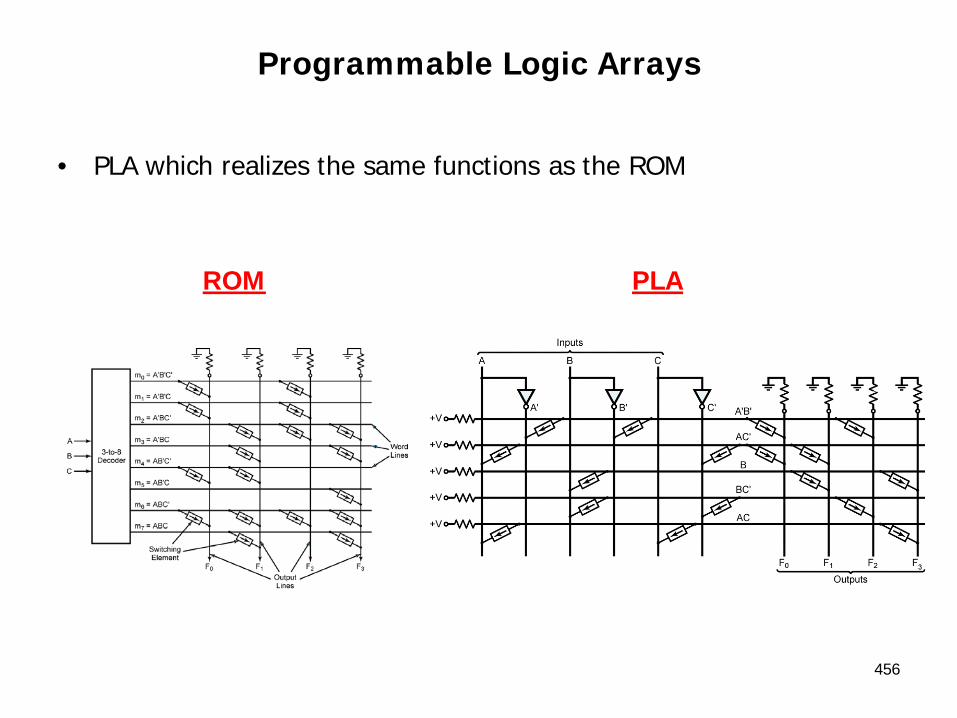
Programmable Logic Arrays
• PLA which realizes the same functions as the ROM
ROM PLA
456

Programmable Logic Arrays
• Product terms are formed in the AND array by connecting switching elements at appropriate points in the array
457
458
Programmable Array Logic

Programmable Array Logic
• Programmable Array Logic … PAL
• The PAL is a special case of the PLA in which …
– The AND array is programmable and the OR array is fixed
• Because only the AND array is programmable …
– The PAL is less expensive than the more general PLA … and …
• The PAL is easier to program
459
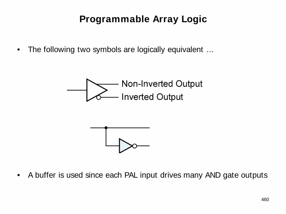
Programmable Array Logic
• The following two symbols are logically equivalent …
• A buffer is used since each PAL input drives many AND gate outputs
460
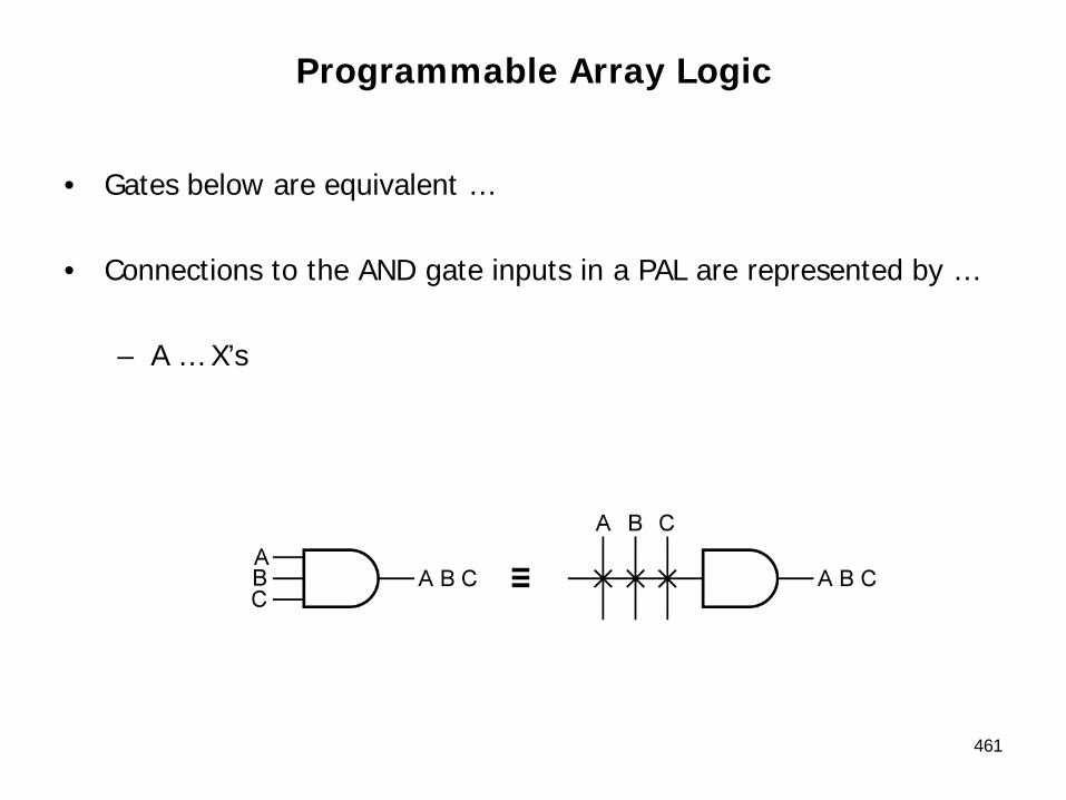
Programmable Array Logic
• Gates below are equivalent …
• Connections to the AND gate inputs in a PAL are represented by …
– A … X’s
461

462
Complex Programmable Logic Devices

Complex Programmable Logic Devices
• As integrated circuit technology continues to improve …
– More and more gates can be placed on a single chip
• This has allowed the development of …
– Complex programmable logic devices … CPLDs ...
463

Complex Programmable Logic Devices
• Instead of a single PAL or PLA on a chip …
– Many PALs or PLAs can be placed on a single CPLD chip and interconnected
• When storage elements such as flip-flops are also included on the same integrated circuit (IC) …
– A small digital system can be implemented with a single CPLD
464

465
Field-Programmable Gate Arrays

Field-Programmable Gate Arrays
• Field-Programmable Gate Array … FPGA
– Is an IC that contains an array of identical logic cells with programmable interconnections
• The user can program the functions realized by each logic cell and the connections between the cells
466
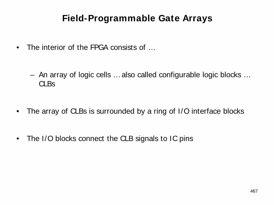
Field-Programmable Gate Arrays
• The interior of the FPGA consists of …
– An array of logic cells … also called configurable logic blocks … CLBs
• The array of CLBs is surrounded by a ring of I/O interface blocks
• The I/O blocks connect the CLB signals to IC pins
467

468
Shannon′s Expansion Theorem
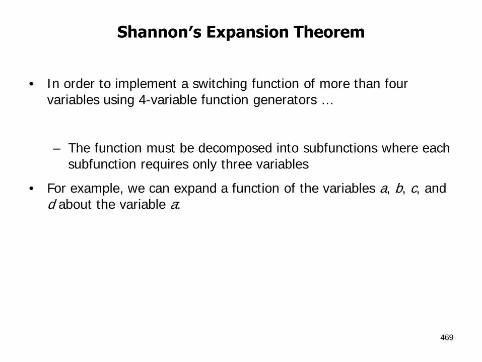
Shannon′s Expansion Theorem
• In order to implement a switching function of more than four variables using 4-variable function generators …
– The function must be decomposed into subfunctions where each subfunction requires only three variables
• For example, we can expand a function of the variables a, b, c, and d about the variable a:
469
470
Chapter 10 …
INTRODUCTION TO VHDL

VHDL Description of Combinational Circuits
• VHDL …
– Very high speed integrated circuits Hardware Description Language
• A VHDL signal is used to … describe a signal in a physical system
471
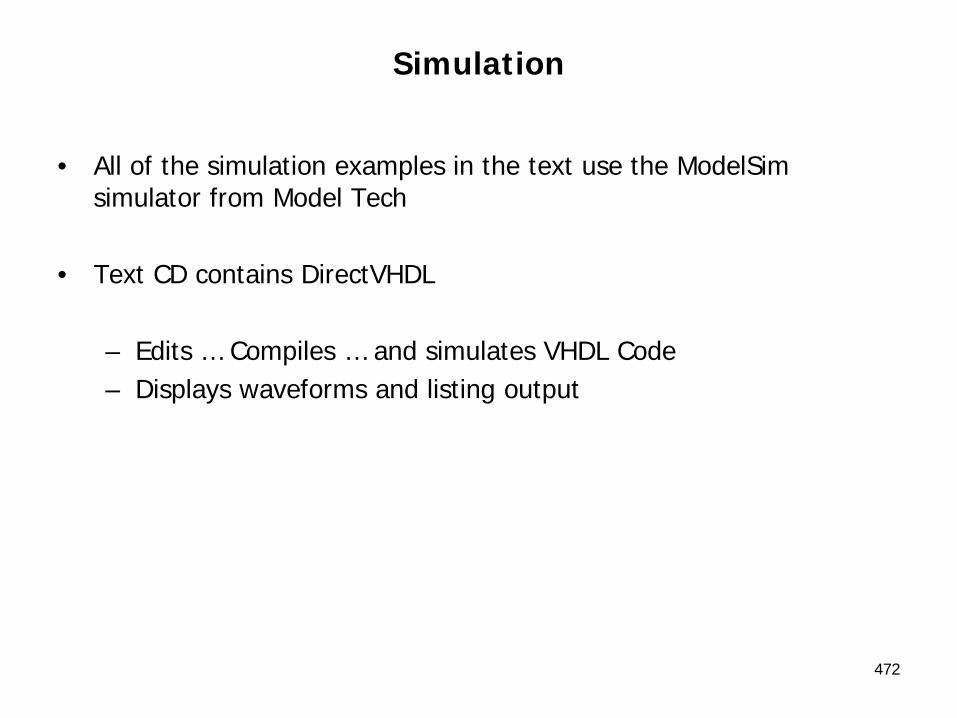
Simulation
• All of the simulation examples in the text use the ModelSimsimulator from Model Tech
• Text CD contains DirectVHDL
– Edits … Compiles … and simulates VHDL Code– Displays waveforms and listing output
472

Simulation - Results
473

Summary
• After the VHDL code for a digital system has been simulated to verify that it works correctly …
– The VHDL code can be synthesized to produce a list of required components and their interconnections
• The synthesizer output can then be used to implement the digital system using specific hardware such as a CPLD or FPGA
• The CAD software used for implementation generates the necessary information to program the CPLD or FPGA hardware
• The synthesis and implementation of digital logic from VHDL code will be discussed in more detail this semester
474

Summary
• We covered the basics of VHDL
• We have shown how to use VHDL to model combinational logic and how to construct a VHDL module using an entity-architecture pair
• Because VHDL is a hardware description language … it differs from an ordinary programming language in several ways
– Most importantly … VHDL statements execute concurrently because they must model real hardware in which the components are all in operation at the same time
475

476
Questions?

477
Lab

478
LABS
• To be discussed next week

479
Next Week …

480
Next Week Topics
• Chapter 11 … Latches and Flip-Flops
• Pages 317 – 347

481
Home Work

482
Homework
1. Send an email with your email address or addresses (for class distribution list)
2. Send me your UMS# (will be on your Access Card) so I can get access to BL-420 and EB-321 (computer labs), if you currently do not have access
3. Read … – Chapter 11 … Latches and Flip-Flops
– Pages 317 – 347