local-fields and disorder effects in free-standing and embedded si nanocrystallites
TRANSCRIPT
Phys. Status Solidi B 247, No. 8, 2113–2117 (2010) / DOI 10.1002/pssb.200983926 p s sb
statu
s
soli
di
www.pss-b.comph
ysi
ca
basic solid state physics
Local-fields and disorder effects in
free-standing and embedded Si nanocrystallitesRoberto Guerra*,1, Elena Degoli2, Margherita Marsili3, Olivia Pulci3, and Stefano Ossicini2
1 S3-Istituto Nanoscienze CNR and Dipartimento di Fisica, Universita di Modena e Reggio Emilia, via Campi 213/A, 41123 Modena,
Italy2 S3-Istituto Nanoscienze CNR and Dipartimento di Scienze e Metodi dell’Ingegneria, Universita di Modena e Reggio Emilia,
via Amendola 2 Pad. Morselli, 42122 Reggio Emilia, Italy3 Dipartimento di Fisica dell’Universita di Roma Tor Vergata, European Theoretical Spectroscopy Facility (ETSF), CNR-INFM-SMC,
NAST, via della Ricerca Scientifica, 00133 Roma, Italy
Received 4 September 2009, revised 28 January 2010, accepted 17 February 2010
Published online 18 June 2010
Keywords ab initio calculations, nanocrystals, optical properties, silicon
* Corresponding author: e-mail [email protected], Phone: þ39 0522 522116, Fax: þ39 059 374794
The case study of a 32-atoms Si nanocrystallite (NC) embedded
in a SiO2 matrix, both crystalline and amorphous, or free-
standing with different conditions of passivation and strain is
analyzed through ab-initio approaches. The Si32/SiO2 hetero-
junction shows a type I band offset highlighting a separation
between the NC plus the interface and the matrix around. The
consequence of this separation is the possibility to correctly
reproduce the low energy electronic and optical properties of
the composed system simply by studying the suspended NC
plus interface oxygens with the appropriate strain. Moreover,
through the definition of an optical absorption threshold we
found that, beside the quantum confinement trend, the
amorphization introduces an additional redshift that increases
with increasing NC size, i.e. the gap tends faster to the bulk
limit. Finally, the important changes in the calculated DFT-
RPA optical spectra upon inclusion of local fields point towards
the need of a proper treatment of the optical response of the
interface region.
� 2010 WILEY-VCH Verlag GmbH & Co. KGaA, Weinheim
1 Introduction Light emission in the visible spectralrange and at room temperature has been observed in the lasttwo decades in porous Si before and in nanostructured Siafter. Si nanocrystallites embedded in a silicon dioxidematrix, in particular, have attracted much attention in recentyears [1–3]. In these structures, Si acts as the low-energygap material. The strong quantum confinement induced bythe dielectric matrix enlarges the band-gap and increasesthe spatial overlap of the electron and hole wave functions,thus increasing the spontaneous emission rate and shiftingthe emission peak to energies higher than bulk Si band-gap.Despite the large number of experiments and theoreticalstudies, many questions are still open concerning the natureof the optical properties of Si-NCs embedded in a silicamatrix. Actually, too many parameters, like size, shape,strain, and interface structure, influence the spectralresponse of the system. The characterization of thesequantities is thus of fundamental importance in order todetermine the best condition for light emission andoptical gain.
In this work, we present DFT calculations on a crystallineand amorphous 32-atoms Si-NC, passivated with hydrogens,OH groups, and embedded in a SiO2 matrix. The comparisonbetween the embedded and suspended NCs can give someinsight on the role played by the strain in the determination ofthe electronic and optical properties of the composed system,while the different passivation regimes can reveal thecontribution given separately by the NC, the interface andthe matrix to the properties of the whole system.
The paper is organized as follows. A description of thetheoretical methods and of the systems is given in Section 2.The electronic and optical properties of the consideredsystems are analyzed in Section 3 while conclusions arepresented in Section 4.
2 Theoretical method Ab-initio calculations ofstructural, electronic, and optical properties for a 32 atomsSi-NC with different surface passivations or embedded in aSiO2 matrix have been carried out within the densityfunctional theory (DFT) [9]. For what concerns the
� 2010 WILEY-VCH Verlag GmbH & Co. KGaA, Weinheim

2114 R. Guerra et al.: Free-standing and embedded Si nanocrystallitesp
hys
ica ssp st
atu
s
solid
i b
embedding medium we have also analyzed the role of thedisorder by considering a crystalline phase or an amorphousglass. For the crystalline structure we have considered acubic cell (of side L’ 2:1 nm) of b-cristobalite (BC) SiO2
which is well known to give rise to one of the simplest Si/SiO2 interface because of its diamond-like structure [4]. TheNC/matrix crystalline structure has been obtained from aSi216O432 matrix by removing the 36 oxygens included in asphere of radius 0.6 nm placed at the center of the cubicsupercell (see Fig. 1, top panel). The result is a structure of216 Si and 396 O atoms with 32 Si bonded together to form asmall crystalline skeleton with Td local symmetry beforerelaxation. In such core, Si atoms show a larger bond length(3.1 A) with respect to that of the Si bulk structure (2.35 A).No defects (dangling bonds) are present at the interface andall the O atoms at the NC surface are single bonded with theSi atoms of the cluster. The dimension of the matrixpreserves a separation of at least 1 nm between the NCsreplica, ensuring a proper shielding of the introduced strain[5–7]. The optimized structure has been achieved by fullyrelaxing the atomic positions and the cell shape and size. Thehost matrix gets distorted after the relaxation (essentially dueto the metastable nature of the BC), producing an opticalbehavior similar to that of a completely amorphized silica,but with practically irrelevant effects on the NC crystallinity.Therefore, the final system should be considered more like acrystalline NC in an amorphous SiO2.
Together with the crystalline structure, the complemen-tary case of an amorphous silica (a-SiO2) has beenconsidered. The glass model has been generated by classicalmolecular dynamics (MD) simulations of quenching from a
� 2010 WILEY-VCH Verlag GmbH & Co. KGaA, Weinheim
melt using semi-empirical ionic potentials [8]. The amor-phous dot structure has been obtained starting from aSi216O432 amorphous silica cell by removing the 40 oxygenatoms included in a sphere of radius 0.6 nm placed at thecenter of the cell, as shown in Fig. 1 (bottom panel).Calculations of both the crystalline and amorphous struc-tures have been performed using the SIESTA code [10, 11]with core-corrected Troullier-Martins pseudopotentials anda cutoff of 150Ry on density. No additional external pressureor stress were applied. Atomic positions and cell parametershave been left totally free to move. We note that thecrystalline and the amorphous clusters present a nearest-neighbor distance of about 2.46 A, strained respect to thetypical Si-bulk value (2.35 A), in good agreement with theoutcomes of Yilmaz et al. [12].
In parallel to the crystalline and amorphous Si32/SiO2
systems, three other structures have been studied: (i) the purematrix (in the same phases as used for the embedded NCcalculations), (ii) the isolated NCs as extracted from therelaxed NC-silica complexes and capped by hydrogen atoms(Si32–H), and (iii) the NCs together with the first interfaceoxygens extracted as in point (ii) and then passivated byhydrogen atoms (Si32–OH). In the last two cases only thehydrogen atoms have been relaxed. The goal is to distinguishbetween the properties that depend only on the embeddedNC from those that are instead influenced by the presence ofthe matrix. The comparison of the results relative to differentpassivation regimes (H or OH groups) could give someinsight on the role played by the interface region. As lastpoint, the structures obtained as in point (ii) and (iii) havebeen fully relaxed in order to infer, through the comparison
Figure 1 (online color at: www.pss-b.com)Stick and ball pictures of the final optimizedstructure of Si32 in b-cristobalite matrix (toppanels) or in amorphous glass (a-SiO2)(bottompanels). Red (dark gray) spheres represent theO atoms, cyan (gray) the Si of the matrix, andyellow (light gray) the Si atoms of the NC. Onthe structures, Kohn-Sham orbitals at 10% oftheir maximum amplitude are reported. Inwhite are the sum of all band-edges orbitalslocalized on the NC while in black is first thestate delocalized on the matrix: a) NC: fromHOMO to HOMO� 15, matrix: HOMO� 16,b) NC: from LUMO to LUMOþ 17, matrix:LUMOþ 18, c) NC: from HOMO toHOMO� 8, matrix: HOMO� 9, d) NC: fromLUMO to LUMOþ 18, matrix: LUMOþ 19.
www.pss-b.com
Phys. Status Solidi B 247, No. 8 (2010) 2115
Original
Paper
with the unrelaxed structures, the role played the straininduced by the lattice mismatch between Si and SiO2.
Electronic and optical properties of the relaxed structureshave been obtained in the framework of DFT, using theESPRESSO package [13]. Calculations have been performedusing norm-conserving pseudopotentials within the LDAapproximation with a Ceperley-Alder exchange-correlationpotential, as parametrized by Perdew-Zunger. An energycutoff of 60 Ry on the plane wave basis has been employed.
Local fields (LF) contribution to the optical properties inthe random phase approximation (RPA) has also beencomputed using the EXC code [14].
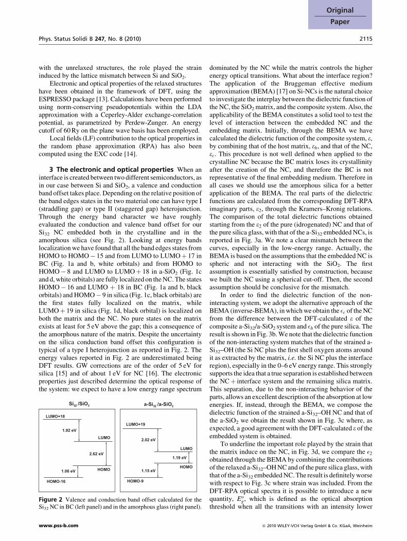
3 The electronic and optical properties When aninterface is created between two different semiconductors, asin our case between Si and SiO2, a valence and conductionband offset takes place. Depending on the relative position ofthe band edges states in the two material one can have type I(straddling gap) or type II (staggered gap) heterojunction.Through the energy band character we have roughlyevaluated the conduction and valence band offset for ourSi32 NC embedded both in the crystalline and in theamorphous silica (see Fig. 2). Looking at energy bandslocalization we have found that all the band edges states fromHOMO to HOMO� 15 and from LUMO to LUMOþ 17 inBC (Fig. 1a and b, white orbitals) and from HOMO toHOMO� 8 and LUMO to LUMOþ 18 in a-SiO2 (Fig. 1cand d, white orbitals) are fully localized on the NC. The statesHOMO� 16 and LUMO þ 18 in BC (Fig. 1a and b, blackorbitals) and HOMO� 9 in silica (Fig. 1c, black orbitals) arethe first states fully localized on the matrix, whileLUMOþ 19 in silica (Fig. 1d, black orbital) is localized onboth the matrix and the NC. No pure states on the matrixexists at least for 5 eV above the gap; this a consequence ofthe amorphous nature of the matrix. Despite the uncertaintyon the silica conduction band offset this configuration istypical of a type I heterojunction as reported in Fig. 2. Theenergy values reported in Fig. 2 are underestimated beingDFT results. GW corrections are of the order of 5 eV forsilica [15] and of about 1 eV for NC [16]. The electronicproperties just described determine the optical response ofthe system: we expect to have a low energy range spectrum
Figure 2 Valence and conduction band offset calculated for theSi32 NC in BC (left panel) and in the amorphous glass (right panel).
www.pss-b.com
dominated by the NC while the matrix controls the higherenergy optical transitions. What about the interface region?The application of the Bruggeman effective mediumapproximation (BEMA) [17] on Si-NCs is the natural choiceto investigate the interplay between the dielectric function ofthe NC, the SiO2 matrix, and the composite system. Also, theapplicability of the BEMA constitutes a solid tool to test thelevel of interaction between the embedded NC and theembedding matrix. Initially, through the BEMA we havecalculated the dielectric function of the composite system, e,by combining that of the host matrix, eh, and that of the NC,ec. This procedure is not well defined when applied to thecrystalline NC because the BC matrix loses its crystallinityafter the creation of the NC, and therefore the BC is notrepresentative of the final embedding medium. Therefore inall cases we should use the amorphous silica for a betterapplication of the BEMA. The real parts of the dielectricfunctions are calculated from the corresponding DFT-RPAimaginary parts, e2, through the Kramers–Kronig relations.The comparison of the total dielectric functions obtainedstarting from the e2 of the pure (idrogenated) NC and that ofthe pure silica glass, with that of the a-Si32 embedded NCs, isreported in Fig. 3a. We note a clear mismatch between thecurves, especially in the low-energy range. Actually, theBEMA is based on the assumptions that the embedded NC isspheric and not interacting with the SiO2. The firstassumption is essentially satisfied by construction, becausewe built the NC using a spherical cut-off. Then, the secondassumption should be conclusive for the mismatch.
In order to find the dielectric function of the non-interacting system, we adopt the alternative approach of theBEMA (inverse-BEMA), in which we obtain the �c of the NCfrom the difference between the DFT-calculated e of thecomposite a-Si32/a-SiO2 system and �h of the pure silica. Theresult is shown in Fig. 3b. We note that the dielectric functionof the non-interacting system matches that of the strained a-Si32–OH (the Si NC plus the first shell oxygen atoms aroundit as extracted by the matrix, i.e. the Si NC plus the interfaceregion), especially in the 0–6 eV energy range. This stronglysupports the idea that a true separation is established betweenthe NCþ interface system and the remaining silica matrix.This separation, due to the non-interacting behavior of theparts, allows an excellent description of the absorption at lowenergies. If, instead, through the BEMA, we compose thedielectric function of the strained a-Si32–OH NC and that ofthe a-SiO2 we obtain the result shown in Fig. 3c where, asexpected, a good agreement with the DFT-calculated e of theembedded system is obtained.
To underline the important role played by the strain thatthe matrix induce on the NC, in Fig. 3d, we compare the �2
obtained through the BEMA by combining the contributionsof the relaxed a-Si32–OH NC and of the pure silica glass, withthat of the a-Si32 embedded NC. The result is definitely worsewith respect to Fig. 3c where strain was included. From theDFT-RPA optical spectra it is possible to introduce a newquantity, Eo
g, which is defined as the optical absorptionthreshold when all the transitions with an intensity lower
� 2010 WILEY-VCH Verlag GmbH & Co. KGaA, Weinheim

2116 R. Guerra et al.: Free-standing and embedded Si nanocrystallitesp
hys
ica ssp st
atu
s
solid
i b
a)
0
0.5
1
1.5
2
2.5
3
3.5
4
4.5
0 2 4 6 8 10 12
ε(ω
) (a
rb.u
.)
Energy (eV)
Re
Im
a-Si32/a-SiO2Bruggeman
b)
0
0.5
1
1.5
2
2.5
0 2 4 6 8 10 12
ε(ω
) (a
rb.u
.)
Energy (eV)
Im
Rea-Si32-OH
inverse-Bruggeman
c)
0
0.5
1
1.5
2
2.5
3
3.5
4
4.5
0 2 4 6 8 10 12
ε(ω
) (a
rb.u
.)
Energy (eV)
Re
Im a-Si32/a-SiO2Bruggeman
d)
0
0.5
1
1.5
2
2.5
3
3.5
4
4.5
0 2 4 6 8 10 12
ε(ω
) (a
rb.u
.)
Energy (eV)
Im
Re
a-Si32/a-SiO2Bruggeman
Figure 3 Comparisonbetween thedielectric functionofa) thea-Si32/a-SiO2 and thatobtainedbytheBEMAcomposing thestraineda-Si32–H NCs and the a-SiO2, b) the strained a-Si32–OH and that obtained by the inverse-BEMA composing the a-Si32/a-SiO2 and the a-SiO2,c) the a-Si32/a-SiO2 and that obtained by the BEMA composing the strained a-Si32–OH NCs and the a-SiO2, d) the a-Si32/a-SiO2 andthat obtained by the BEMA composing the relaxed a-Si32–OH NCs and the a-SiO2. Real and imaginary parts are indicated by labels.
than 1% of the highest peak are neglected. By neglectingvery low oscillator strength optical transitions we introduce asort of ‘‘instrument resolution’’ that can connect theoreticaland experimental results concerning the optical activityof a system. The obtained Eo
g values for the embeddedsystems are reported in Table 1. Here Eo
g has been calculatedfor Si-NC containing 2, 5, 10, and 32 atoms and comparedwith that of pure silica. While the increasing of the NC sizealways results in a reduction in Eo
g, the effect of theamorphization is to introduce an additional redshift (D) thatprogressively increase and becomes relevant for larger NCs.As a consequence the band gap tends faster to the bulk limitin the amorphous system with respect to the crystalline one.Finally, we investigated the optical properties of the Si32 anda-Si32 embedded NCs. In accordance with Delerue andcoworkers [18] that found, for Si-NC larger than 1.2 nm (this
Table 1 Calculated Eog values (in eV) for different size Si nano-
crystals embedded in crystalline or amorphous silica, comparedwith that of pure SiO2. In the last line the difference between thecrystalline and amorphous case are reported.
SiO2 Si2/SiO2 Si5/SiO2 Si10/SiO2 Si32/SiO2
crystalline 6.72 5.66 4.20 3.06 2.46amorphous 6.25 5.49 3.76 1.91 1.10D 0.47 0.17 0.44 1.15 1.36
� 2010 WILEY-VCH Verlag GmbH & Co. KGaA, Weinheim
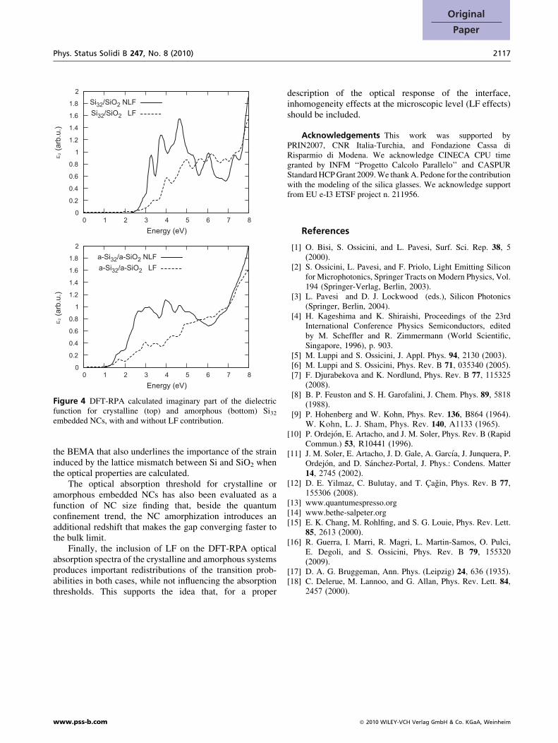
is approximatively our cluster dimension), a mutualcancellation of self-energy and Coulomb corrections, weneglect Many-Body effects. LF effects, instead, seem to havemuch more influence for Si/SiO2 aggregates, as shown in Ref[16]. Hence, we have investigated the optical properties ofthe Si32 and a-Si32 embedded NCs including LF effects. Theresults are shown in Fig. 4. We note a strong similarity of theLF effects on the crystalline and amorphous systems with aprogressive lowering of the spectra intensity as approachingthe low energies. This matches well with the previousresults that associates the low-energy absorption to theinterface. Around the interface a strong charge discontinuity(inhomogeneity) occurs, and this could reasonably explainthe strong LF effects in this region.
4 Conclusions DFT calculations of the electronic andoptical properties of a crystalline and an amorphous 32-atoms Si-NC embedded in a SiO2 matrix are described andcompared with that of the same NC extracted by the matrixwith or without the interface oxygen atoms and passivatedwith H. We find that the NC/matrix heterojunction shows atype I character with the band edges states and consequentlythe low energy range optical spectrum is completely due tothe Si NC plus the interface oxygens. Only higher in energythe response of the system is dominated by the matrix. Thisseparation established between the NCþ interface systemand the silica matrix is also supported by the application of
www.pss-b.com
Phys. Status Solidi B 247, No. 8 (2010) 2117
Original
Paper
0
0.2
0.4
0.6
0.8
1
1.2
1.4
1.6
1.8
2
0 1 2 3 4 5 6 7 8
ε 2(a
rb.u
.)ε 2
(arb
.u.)
Energy (eV)
Si32/SiO2 NLFSi32/SiO2 LF
0
0.2
0.4
0.6
0.8
1
1.2
1.4
1.6
1.8
2
0 1 2 3 4 5 6 7 8
Energy (eV)
a-Si32/a-SiO2 NLFa-Si32/a-SiO2 LF
Figure 4 DFT-RPA calculated imaginary part of the dielectricfunction for crystalline (top) and amorphous (bottom) Si32
embedded NCs, with and without LF contribution.
the BEMA that also underlines the importance of the straininduced by the lattice mismatch between Si and SiO2 whenthe optical properties are calculated.
The optical absorption threshold for crystalline oramorphous embedded NCs has also been evaluated as afunction of NC size finding that, beside the quantumconfinement trend, the NC amorphization introduces anadditional redshift that makes the gap converging faster tothe bulk limit.
Finally, the inclusion of LF on the DFT-RPA opticalabsorption spectra of the crystalline and amorphous systemsproduces important redistributions of the transition prob-abilities in both cases, while not influencing the absorptionthresholds. This supports the idea that, for a proper
www.pss-b.com
description of the optical response of the interface,inhomogeneity effects at the microscopic level (LF effects)should be included.
Acknowledgements This work was supported byPRIN2007, CNR Italia-Turchia, and Fondazione Cassa diRisparmio di Modena. We acknowledge CINECA CPU timegranted by INFM ‘‘Progetto Calcolo Parallelo’’ and CASPURStandard HCP Grant 2009. We thank A. Pedone for the contributionwith the modeling of the silica glasses. We acknowledge supportfrom EU e-I3 ETSF project n. 211956.
References
[1] O. Bisi, S. Ossicini, and L. Pavesi, Surf. Sci. Rep. 38, 5(2000).
[2] S. Ossicini, L. Pavesi, and F. Priolo, Light Emitting Siliconfor Microphotonics, Springer Tracts on Modern Physics, Vol.194 (Springer-Verlag, Berlin, 2003).
[3] L. Pavesi and D. J. Lockwood (eds.), Silicon Photonics(Springer, Berlin, 2004).
[4] H. Kageshima and K. Shiraishi, Proceedings of the 23rdInternational Conference Physics Semiconductors, editedby M. Scheffler and R. Zimmermann (World Scientific,Singapore, 1996), p. 903.
[5] M. Luppi and S. Ossicini, J. Appl. Phys. 94, 2130 (2003).[6] M. Luppi and S. Ossicini, Phys. Rev. B 71, 035340 (2005).[7] F. Djurabekova and K. Nordlund, Phys. Rev. B 77, 115325
(2008).[8] B. P. Feuston and S. H. Garofalini, J. Chem. Phys. 89, 5818
(1988).[9] P. Hohenberg and W. Kohn, Phys. Rev. 136, B864 (1964).
W. Kohn, L. J. Sham, Phys. Rev. 140, A1133 (1965).[10] P. Ordejon, E. Artacho, and J. M. Soler, Phys. Rev. B (Rapid
Commun.) 53, R10441 (1996).[11] J. M. Soler, E. Artacho, J. D. Gale, A. Garcıa, J. Junquera, P.
Ordejon, and D. Sanchez-Portal, J. Phys.: Condens. Matter14, 2745 (2002).
[12] D. E. Yilmaz, C. Bulutay, and T. Cagin, Phys. Rev. B 77,155306 (2008).
[13] www.quantumespresso.org[14] www.bethe-salpeter.org[15] E. K. Chang, M. Rohlfing, and S. G. Louie, Phys. Rev. Lett.
85, 2613 (2000).[16] R. Guerra, I. Marri, R. Magri, L. Martin-Samos, O. Pulci,
E. Degoli, and S. Ossicini, Phys. Rev. B 79, 155320(2009).
[17] D. A. G. Bruggeman, Ann. Phys. (Leipzig) 24, 636 (1935).[18] C. Delerue, M. Lannoo, and G. Allan, Phys. Rev. Lett. 84,
2457 (2000).
� 2010 WILEY-VCH Verlag GmbH & Co. KGaA, Weinheim