lmx19 high speed dual comparator (rev. b) · lm119 –55 125 lm219 –25 85 °c lm319a, lm319 0 70...
TRANSCRIPT

Product
Folder
Sample &Buy
Technical
Documents
Tools &
Software
Support &Community
An IMPORTANT NOTICE at the end of this data sheet addresses availability, warranty, changes, use in safety-critical applications,intellectual property matters and other important disclaimers. PRODUCTION DATA.
LM119, LM219, LM319SNOSBJ2B –AUGUST 2000–REVISED JANUARY 2016
LMx19 High Speed Dual Comparator
1
1 Features1• Two Independent Comparators• Operates from a Single 5-V Supply• Typically 80-ns Response Time at ±15 V• Minimum Fan-out of 2 Each Side• Maximum Input Current of 1 μA Over
Temperature• Inputs and Outputs can be Isolated from System
Ground• High Common-Mode Slew Rate
Connection Diagram
Typical Application - Relay Driver
2 DescriptionThe LM119 series are precision high-speed dualcomparators fabricated on a single monolithic chip.They are designed to operate over a wide range ofsupply voltages down to a single 5-V logic supply andground. They have higher gain and lower inputcurrents than devices such as the LM710. Theuncommitted collector of the output stage makes theLM119 compatible with RTL, DTL, and TTL, as wellas capable of driving lamps and relays at currents ofup to 25 mA.
The LM319A offers improved precision over thestandard LM319, with tighter tolerances on offsetvoltage, offset current, and voltage gain.
Although designed primarily for applications requiringoperation from digital logic supplies, the LM119 seriesare fully specified for power supplies up to ±15 V.The series features faster response than the LM111,at the expense of higher power dissipation. However,the high-speed, wide operating voltage range and lowpackage count make the LM119 more versatile thanolder devices such as the LM711.
The LM119 is specified from −55°C to +125°C, theLM219 is specified from −25°C to +85°C, and theLM319A and LM319 are specified from 0°C to +70°C.
Device Information(1)
PART NUMBER PACKAGE BODY SIZE (NOM)
LM119, LM219,LM319
TO-100 (10) 8.96 mm × 8.96 mm
CDIP (14) 6.67 mm × 19.56mm
(1) For all available packages, see the orderable addendum atthe end of the data sheet.
2
LM119, LM219, LM319SNOSBJ2B –AUGUST 2000–REVISED JANUARY 2016 www.ti.com
Product Folder Links: LM119 LM219 LM319
Submit Documentation Feedback Copyright © 2000–2016, Texas Instruments Incorporated
Table of Contents1 Features .................................................................. 12 Description ............................................................. 13 Revision History..................................................... 24 Pin Configuration and Functions ......................... 35 Specifications......................................................... 4
5.1 Absolute Maximum Ratings ...................................... 45.2 ESD Ratings.............................................................. 45.3 Thermal Information .................................................. 45.4 Electrical Characteristics LM119, LM219.................. 55.5 Electrical Characteristics LM319, LM319A ............... 65.6 Typical Characteristics .............................................. 7
6 Detailed Description ............................................ 106.1 Functional Block Diagram ....................................... 10
7 Application and Implementation ........................ 117.1 Typical Applications ................................................ 11
8 Device and Documentation Support.................. 128.1 Related Links .......................................................... 128.2 Community Resources............................................ 128.3 Trademarks ............................................................. 128.4 Electrostatic Discharge Caution.............................. 128.5 Glossary .................................................................. 12
9 Mechanical, Packaging, and OrderableInformation ........................................................... 12
3 Revision History
Changes from Revision A (May 2004) to Revision B Page
• Changed datasheet to new TI format from National. ............................................................................................................. 1• Added Pin Functions and Thermal Information tables, the Device and Documentation Support section, and
Mechanical, Packaging, and Orderable Information section .................................................................................................. 1

3
LM119, LM219, LM319www.ti.com SNOSBJ2B –AUGUST 2000–REVISED JANUARY 2016
Product Folder Links: LM119 LM219 LM319
Submit Documentation FeedbackCopyright © 2000–2016, Texas Instruments Incorporated
4 Pin Configuration and Functions
D, J, or NFF Package14-Pins CDIP and PDIP
Top ViewLME Package
10-Pins TO-100 (Metal Can Package)Top View
NAD Package10-Pins CFP
Top View
Pin FunctionsPIN I/O DESCRIPTION
NAME NO.(D, J, NFF 14)
NO.(LME 10)
NO.(NAD 10)
OUTPUT 1 1 12 1 O Comparator 1 outputGND 1 2 3 2 G Comparator 1 ground connectionINPUT 1+ 3 4 3 I Comparator 1 inputINPUT 1- 4 5 4 I Comparator 1 inputV- 5 6 5 P Negative supply voltageOUTPUT 2 6 7 6 O Comparator 2 outputGND 2 7 8 7 G Comparator 2 ground connectionINPUT 2+ 8 9 8 I Comparator 2 inputINPUT 2- 9 10 9 I Comparator 2 inputV+ 10 11 10 P Positive supply voltageNC 1,2,13,14 No connect. Do not connect to ground.
4
LM119, LM219, LM319SNOSBJ2B –AUGUST 2000–REVISED JANUARY 2016 www.ti.com
Product Folder Links: LM119 LM219 LM319
Submit Documentation Feedback Copyright © 2000–2016, Texas Instruments Incorporated
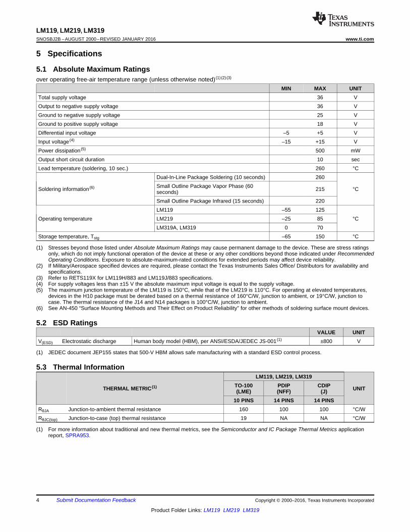
(1) Stresses beyond those listed under Absolute Maximum Ratings may cause permanent damage to the device. These are stress ratingsonly, which do not imply functional operation of the device at these or any other conditions beyond those indicated under RecommendedOperating Conditions. Exposure to absolute-maximum-rated conditions for extended periods may affect device reliability.
(2) If Military/Aerospace specified devices are required, please contact the Texas Instruments Sales Office/ Distributors for availability andspecifications.
(3) Refer to RETS119X for LM119H/883 and LM119J/883 specifications.(4) For supply voltages less than ±15 V the absolute maximum input voltage is equal to the supply voltage.(5) The maximum junction temperature of the LM119 is 150°C, while that of the LM219 is 110°C. For operating at elevated temperatures,
devices in the H10 package must be derated based on a thermal resistance of 160°C/W, junction to ambient, or 19°C/W, junction tocase. The thermal resistance of the J14 and N14 packages is 100°C/W, junction to ambient.
(6) See AN-450 “Surface Mounting Methods and Their Effect on Product Reliability” for other methods of soldering surface mount devices.
5 Specifications
5.1 Absolute Maximum Ratingsover operating free-air temperature range (unless otherwise noted) (1) (2) (3)
MIN MAX UNITTotal supply voltage 36 VOutput to negative supply voltage 36 VGround to negative supply voltage 25 VGround to positive supply voltage 18 VDifferential input voltage –5 +5 VInput voltage (4) –15 +15 VPower dissipation (5) 500 mWOutput short circuit duration 10 secLead temperature (soldering, 10 sec.) 260 °C
Soldering information (6)
Dual-In-Line Package Soldering (10 seconds) 260
°CSmall Outline Package Vapor Phase (60seconds) 215
Small Outline Package Infrared (15 seconds) 220
Operating temperatureLM119 –55 125
°CLM219 –25 85LM319A, LM319 0 70
Storage temperature, Tstg –65 150 °C
(1) JEDEC document JEP155 states that 500-V HBM allows safe manufacturing with a standard ESD control process.
5.2 ESD RatingsVALUE UNIT
V(ESD) Electrostatic discharge Human body model (HBM), per ANSI/ESDA/JEDEC JS-001 (1) ±800 V
(1) For more information about traditional and new thermal metrics, see the Semiconductor and IC Package Thermal Metrics applicationreport, SPRA953.
5.3 Thermal Information
THERMAL METRIC (1)
LM119, LM219, LM319
UNITTO-100(LME)
PDIP(NFF)
CDIP(J)
10 PINS 14 PINS 14 PINSRθJA Junction-to-ambient thermal resistance 160 100 100 °C/WRθJC(top) Junction-to-case (top) thermal resistance 19 NA NA °C/W

5
LM119, LM219, LM319www.ti.com SNOSBJ2B –AUGUST 2000–REVISED JANUARY 2016
Product Folder Links: LM119 LM219 LM319
Submit Documentation FeedbackCopyright © 2000–2016, Texas Instruments Incorporated
(1) The offset voltages and offset currents given are the maximum values required to drive the output within a volt of either supply with a 1-mA load. Thus, these parameters define an error band and take into account the worst case effects of voltage gain and inputimpedance.
(2) Output is pulled up to 15 V through a 1.4-kW resistor.(3) The response time specified is for a 100-mV input step with 5-mV overdrive.
5.4 Electrical Characteristics LM119, LM219These specifications apply for VS = ±15 V, and the Ground pin at ground, and −55°C ≤ TA ≤ +125°C, unless otherwise stated.With the LM219, all temperature specifications are limited to −25°C ≤ TA ≤ +85°C. The offset voltage, offset current and biascurrent specifications apply for any supply voltage from a single 5-V supply up to ±15-V supplies. Do not operate the devicewith more than 16 V from ground to VS.
PARAMETER TEST CONDITIONS MIN TYP MAX UNITInput Offset Voltage (1) TA = 25°C, RS ≤ 5k 0.7 4 mVInput Offset Current (1) TA = 25°C 30 75 nAInput Bias Current TA = 25°C 150 500 nAVoltage Gain TA = 25°C (2) 10 40 V/mVResponse Time (3) TA = 25°C, VS = ±15 V 80 ns
Saturation Voltage VIN ≤ −5 mV, IOUT = 25 mATA = 25°C 0.75 1.5 V
Output Leakage Current VIN ≥ 5 mV, VOUT = 35 VTA = 25°C 0.2 2 µA
Input Offset Voltage (1) RS ≤ 5k 7 mVInput Offset Current (1) 100 nAInput Bias Current 1000 nA
Input Voltage RangeVS = ±15 V –12 ±13 +12
VV+ = 5 V, V- = 0 1 3
Saturation Voltage
V+ ≥ 4.5 V, V− = 0VIN ≤ −6 mV, ISINK ≤ 3.2 mA
VTA ≥ 0°C 0.23 0.4TA ≤ 0°C 0.6
Output Leakage Current VIN ≥ 5 mV, VOUT = 35 V, V− = VGND= 0 V 1 10 µA
Differential Input Voltage ±5 VPositive Supply Current TA = 25°C, V+ = 5 V, V− = 0 4.3 mAPositive Supply Current TA = 25°C, VS = ±15 V 8 11.5 mANegative Supply Current TA = 25°C, VS = ±15 V 3 4.5 mA

6
LM119, LM219, LM319SNOSBJ2B –AUGUST 2000–REVISED JANUARY 2016 www.ti.com
Product Folder Links: LM119 LM219 LM319
Submit Documentation Feedback Copyright © 2000–2016, Texas Instruments Incorporated
(1) The offset voltages and offset currents given are the maximum values required to drive the output within a volt of either supply with a 1-mA load. Thus, these parameters define an error band and take into account the worst case effects of voltage gain and inputimpedance.
(2) Output is pulled up to 15 V through a 1.4-kW resistor.(3) The response time specified is for a 100-mV input step with 5-mV overdrive.
5.5 Electrical Characteristics LM319, LM319AThese specifications apply for VS = ±15 V, and 0°C ≤ TA ≤ 70°C, unless otherwise stated. The offset voltage, offset current,and bias current specifications apply for any supply voltage from a single 5-V supply up to ±15-V supplies. Do not operate thedevice with more than 16 V from ground to VS.
PARAMETER TEST CONDITIONSLM319A LM319
UNITMIN TYP MAX MIN TYP MAX
Input Offset Voltage (1) TA = 25°C, RS ≤ 5k 0.5 1 2 8 mVInput Offset Current (1) TA = 25°C 20 40 80 200 nAInput Bias Current TA = 25°C 150 500 250 1000 nAVoltage Gain TA = 25°C (2) 20 40 8 40 V/mVResponse Time (3) TA = 25°C, VS = ±15 V 80 80 ns
Saturation Voltage VIN ≤ −10 mV, IOUT = 25 mATA = 25°C 0.75 1.5 0.75 1.5 V
Output Leakage Current VIN ≥ 10 mV, VOUT = 35 VV− = VGND = 0 V, TA = 25°C 0.2 10 0.2 10 µA
Input Offset Voltage (1) RS ≤ 5k 10 10 mVInput Offset Current (1) 300 300 nAInput Bias Current 1000 1200 nA
Input Voltage RangeVS = ±15 V ±13 ±13
VV+ = 5 V, V- = 0 1 3 1 3
Saturation Voltage V+ ≥ 4.5 V, V− = 0VIN ≤ −10 mV, ISINK ≤ 3.2 mA 0.3 0.4 0.3 0.4 V
Differential Input Voltage ±5 ±5 VPositive Supply Current TA = 25°C, V+ = 5 V, V− = 0 4.3 4.3 mAPositive Supply Current TA = 25°C, VS = ±15 V 8 12.5 8 12.5 mANegative Supply Current TA = 25°C, VS = ±15 V 3 5 3 5 mA

7
LM119, LM219, LM319www.ti.com SNOSBJ2B –AUGUST 2000–REVISED JANUARY 2016
Product Folder Links: LM119 LM219 LM319
Submit Documentation FeedbackCopyright © 2000–2016, Texas Instruments Incorporated
5.6 Typical Characteristics
5.6.1 Typical Characteristics – LM119, LM119A, LM219
Figure 1. Input Currents Figure 2. Common-Mode Limits
Figure 3. Transfer Function Figure 4. Response Time for Various Input Overdrives
Figure 5. Response Time for Various Input Overdrives Figure 6. Input Characteristics
Figure 7. Response Time for Various Input Overdrives Figure 8. Response Time for Various Input Overdrives
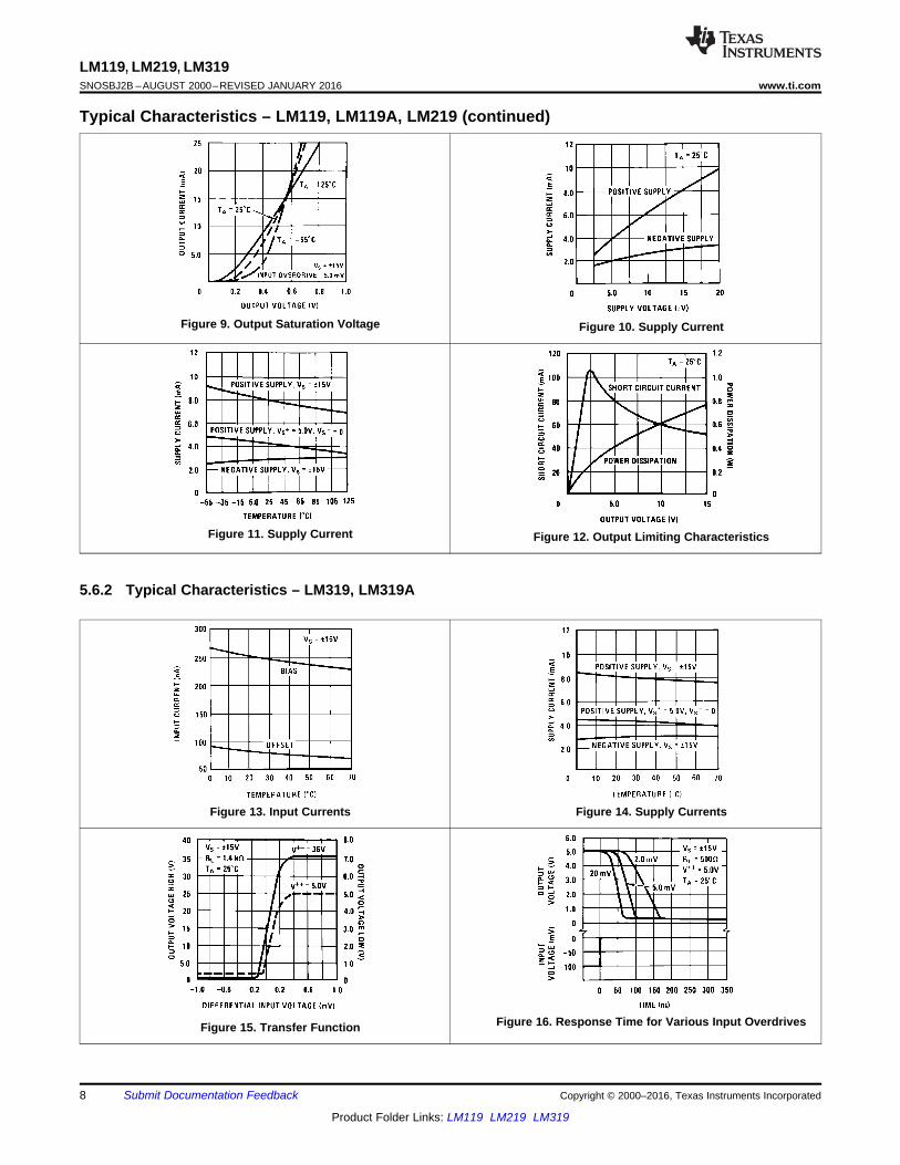
8
LM119, LM219, LM319SNOSBJ2B –AUGUST 2000–REVISED JANUARY 2016 www.ti.com
Product Folder Links: LM119 LM219 LM319
Submit Documentation Feedback Copyright © 2000–2016, Texas Instruments Incorporated
Typical Characteristics – LM119, LM119A, LM219 (continued)
Figure 9. Output Saturation Voltage Figure 10. Supply Current
Figure 11. Supply Current Figure 12. Output Limiting Characteristics
5.6.2 Typical Characteristics – LM319, LM319A
Figure 13. Input Currents Figure 14. Supply Currents
Figure 15. Transfer Function Figure 16. Response Time for Various Input Overdrives
9
LM119, LM219, LM319www.ti.com SNOSBJ2B –AUGUST 2000–REVISED JANUARY 2016
Product Folder Links: LM119 LM219 LM319
Submit Documentation FeedbackCopyright © 2000–2016, Texas Instruments Incorporated
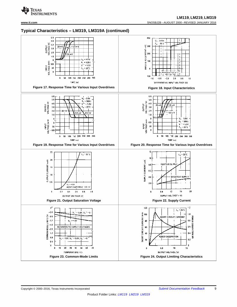
Typical Characteristics – LM319, LM319A (continued)
Figure 17. Response Time for Various Input Overdrives Figure 18. Input Characteristics
Figure 19. Response Time for Various Input Overdrives Figure 20. Response Time for Various Input Overdrives
Figure 21. Output Saturation Voltage Figure 22. Supply Current
Figure 23. Common-Mode Limits Figure 24. Output Limiting Characteristics
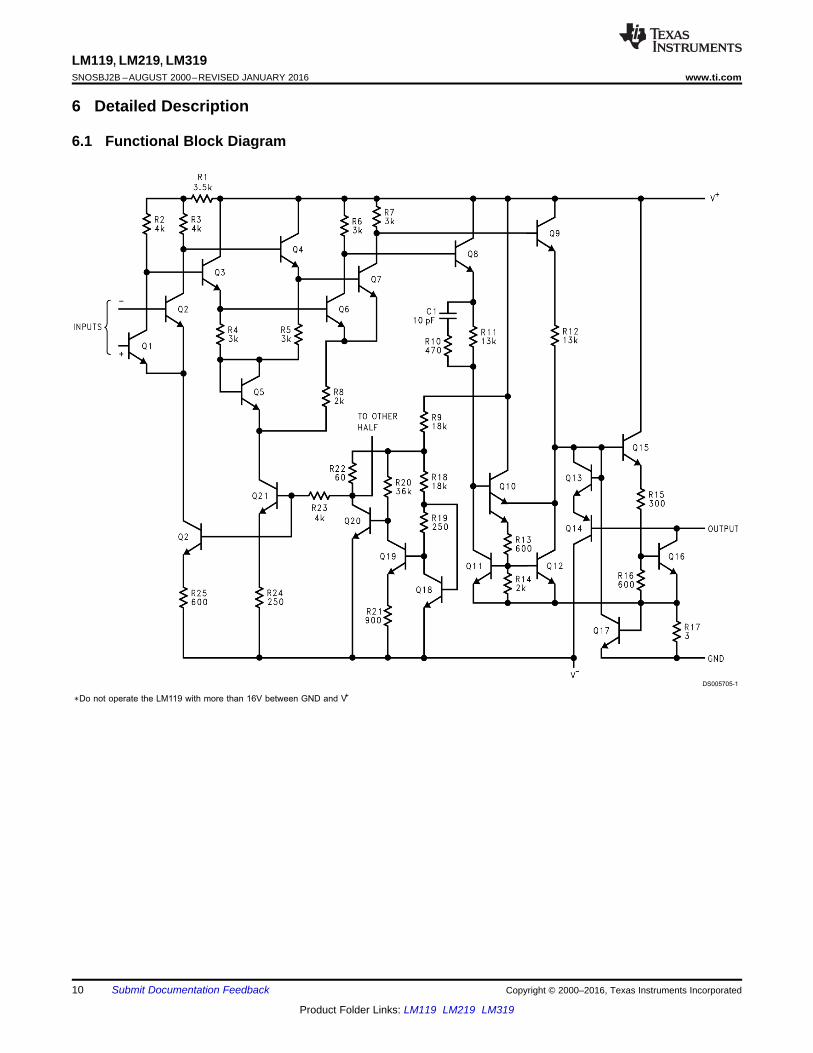
DS005705-1
∗Do not operate the LM119 with more than 16V between GND and V+
10
LM119, LM219, LM319SNOSBJ2B –AUGUST 2000–REVISED JANUARY 2016 www.ti.com
Product Folder Links: LM119 LM219 LM319
Submit Documentation Feedback Copyright © 2000–2016, Texas Instruments Incorporated
6 Detailed Description
6.1 Functional Block Diagram

11
LM119, LM219, LM319www.ti.com SNOSBJ2B –AUGUST 2000–REVISED JANUARY 2016
Product Folder Links: LM119 LM219 LM319
Submit Documentation FeedbackCopyright © 2000–2016, Texas Instruments Incorporated
7 Application and Implementation
NOTEInformation in the following applications sections is not part of the TI componentspecification, and TI does not warrant its accuracy or completeness. TI’s customers areresponsible for determining suitability of components for their purposes. Customers shouldvalidate and test their design implementation to confirm system functionality.
7.1 Typical Applications
7.1.1 Relay Driver
Figure 25. Relay Driver
7.1.2 Window Detector
Figure 26. Window Detector
12
LM119, LM219, LM319SNOSBJ2B –AUGUST 2000–REVISED JANUARY 2016 www.ti.com
Product Folder Links: LM119 LM219 LM319
Submit Documentation Feedback Copyright © 2000–2016, Texas Instruments Incorporated
8 Device and Documentation Support
8.1 Related LinksThe table below lists quick access links. Categories include technical documents, support and communityresources, tools and software, and quick access to sample or buy.
Table 1. Related Links
PARTS PRODUCT FOLDER SAMPLE & BUY TECHNICALDOCUMENTS
TOOLS &SOFTWARE
SUPPORT &COMMUNITY
LM119 Click here Click here Click here Click here Click hereLM219 Click here Click here Click here Click here Click hereLM319 Click here Click here Click here Click here Click here
8.2 Community ResourcesThe following links connect to TI community resources. Linked contents are provided "AS IS" by the respectivecontributors. They do not constitute TI specifications and do not necessarily reflect TI's views; see TI's Terms ofUse.
TI E2E™ Online Community TI's Engineer-to-Engineer (E2E) Community. Created to foster collaborationamong engineers. At e2e.ti.com, you can ask questions, share knowledge, explore ideas and helpsolve problems with fellow engineers.
Design Support TI's Design Support Quickly find helpful E2E forums along with design support tools andcontact information for technical support.
8.3 TrademarksE2E is a trademark of Texas Instruments.All other trademarks are the property of their respective owners.
8.4 Electrostatic Discharge CautionThese devices have limited built-in ESD protection. The leads should be shorted together or the device placed in conductive foamduring storage or handling to prevent electrostatic damage to the MOS gates.
8.5 GlossarySLYZ022 — TI Glossary.
This glossary lists and explains terms, acronyms, and definitions.
9 Mechanical, Packaging, and Orderable InformationThe following pages include mechanical, packaging, and orderable information. This information is the mostcurrent data available for the designated devices. This data is subject to change without notice and revision ofthis document. For browser-based versions of this data sheet, refer to the left-hand navigation.

PACKAGE OPTION ADDENDUM
www.ti.com 17-Mar-2017
Addendum-Page 1
PACKAGING INFORMATION
Orderable Device Status(1)
Package Type PackageDrawing
Pins PackageQty
Eco Plan(2)
Lead/Ball Finish(6)
MSL Peak Temp(3)
Op Temp (°C) Device Marking(4/5)
Samples
LM119H ACTIVE TO-100 LME 10 500 TBD Call TI Call TI -55 to 125 ( LM119H ~ LM119H)
LM119H/NOPB ACTIVE TO-100 LME 10 500 Green (RoHS& no Sb/Br)
Call TI Level-1-NA-UNLIM -55 to 125 ( LM119H ~ LM119H)
LM119J ACTIVE CDIP J 14 25 TBD Call TI Call TI -55 to 125 LM119J
LM319AM NRND SOIC D 14 55 TBD Call TI Call TI 0 to 70 LM319AM
LM319AM/NOPB ACTIVE SOIC D 14 55 Green (RoHS& no Sb/Br)
CU SN Level-1-260C-UNLIM 0 to 70 LM319AM
LM319AMX/NOPB ACTIVE SOIC D 14 2500 Green (RoHS& no Sb/Br)
CU SN Level-1-260C-UNLIM 0 to 70 LM319AM
LM319M NRND SOIC D 14 55 TBD Call TI Call TI 0 to 70 LM319M
LM319M/NOPB ACTIVE SOIC D 14 55 Green (RoHS& no Sb/Br)
CU SN Level-1-260C-UNLIM 0 to 70 LM319M
LM319MX/NOPB ACTIVE SOIC D 14 2500 Green (RoHS& no Sb/Br)
CU SN Level-1-260C-UNLIM 0 to 70 LM319M
LM319N/NOPB ACTIVE PDIP NFF 14 25 Green (RoHS& no Sb/Br)
CU SN Level-1-NA-UNLIM 0 to 70 LM319N
(1) The marketing status values are defined as follows:ACTIVE: Product device recommended for new designs.LIFEBUY: TI has announced that the device will be discontinued, and a lifetime-buy period is in effect.NRND: Not recommended for new designs. Device is in production to support existing customers, but TI does not recommend using this part in a new design.PREVIEW: Device has been announced but is not in production. Samples may or may not be available.OBSOLETE: TI has discontinued the production of the device.
(2) Eco Plan - The planned eco-friendly classification: Pb-Free (RoHS), Pb-Free (RoHS Exempt), or Green (RoHS & no Sb/Br) - please check http://www.ti.com/productcontent for the latest availabilityinformation and additional product content details.TBD: The Pb-Free/Green conversion plan has not been defined.Pb-Free (RoHS): TI's terms "Lead-Free" or "Pb-Free" mean semiconductor products that are compatible with the current RoHS requirements for all 6 substances, including the requirement thatlead not exceed 0.1% by weight in homogeneous materials. Where designed to be soldered at high temperatures, TI Pb-Free products are suitable for use in specified lead-free processes.Pb-Free (RoHS Exempt): This component has a RoHS exemption for either 1) lead-based flip-chip solder bumps used between the die and package, or 2) lead-based die adhesive used betweenthe die and leadframe. The component is otherwise considered Pb-Free (RoHS compatible) as defined above.Green (RoHS & no Sb/Br): TI defines "Green" to mean Pb-Free (RoHS compatible), and free of Bromine (Br) and Antimony (Sb) based flame retardants (Br or Sb do not exceed 0.1% by weightin homogeneous material)
(3) MSL, Peak Temp. - The Moisture Sensitivity Level rating according to the JEDEC industry standard classifications, and peak solder temperature.

PACKAGE OPTION ADDENDUM
www.ti.com 17-Mar-2017
Addendum-Page 2
(4) There may be additional marking, which relates to the logo, the lot trace code information, or the environmental category on the device.
(5) Multiple Device Markings will be inside parentheses. Only one Device Marking contained in parentheses and separated by a "~" will appear on a device. If a line is indented then it is a continuationof the previous line and the two combined represent the entire Device Marking for that device.
(6) Lead/Ball Finish - Orderable Devices may have multiple material finish options. Finish options are separated by a vertical ruled line. Lead/Ball Finish values may wrap to two lines if the finishvalue exceeds the maximum column width.
Important Information and Disclaimer:The information provided on this page represents TI's knowledge and belief as of the date that it is provided. TI bases its knowledge and belief on informationprovided by third parties, and makes no representation or warranty as to the accuracy of such information. Efforts are underway to better integrate information from third parties. TI has taken andcontinues to take reasonable steps to provide representative and accurate information but may not have conducted destructive testing or chemical analysis on incoming materials and chemicals.TI and TI suppliers consider certain information to be proprietary, and thus CAS numbers and other limited information may not be available for release.
In no event shall TI's liability arising out of such information exceed the total purchase price of the TI part(s) at issue in this document sold by TI to Customer on an annual basis.

TAPE AND REEL INFORMATION
*All dimensions are nominal
Device PackageType
PackageDrawing
Pins SPQ ReelDiameter
(mm)
ReelWidth
W1 (mm)
A0(mm)
B0(mm)
K0(mm)
P1(mm)
W(mm)
Pin1Quadrant
LM319AMX/NOPB SOIC D 14 2500 330.0 16.4 6.5 9.35 2.3 8.0 16.0 Q1
LM319MX/NOPB SOIC D 14 2500 330.0 16.4 6.5 9.35 2.3 8.0 16.0 Q1
PACKAGE MATERIALS INFORMATION
www.ti.com 7-Jan-2016
Pack Materials-Page 1

*All dimensions are nominal
Device Package Type Package Drawing Pins SPQ Length (mm) Width (mm) Height (mm)
LM319AMX/NOPB SOIC D 14 2500 367.0 367.0 35.0
LM319MX/NOPB SOIC D 14 2500 367.0 367.0 35.0
PACKAGE MATERIALS INFORMATION
www.ti.com 7-Jan-2016
Pack Materials-Page 2


www.ti.com
PACKAGE OUTLINE
C
A
9.408.51
( 3.56)STAND-OFF
0.860.71
5.84
2.92
8.517.75
5.72 MAX4.704.191.02 MAX
10X 12.7 MIN
10X 0.530.41
STAND-OFF1.020.25
1.140.74
36 TYP
TO-CAN - 5.72 mm max heightLME0010AMETAL CYLINDRICAL PACKAGE
4220604/A 05/2017
NOTES: 1. All linear dimensions are in millimeters. Any dimensions in parenthesis are for reference only. Dimensioning and tolerancing per ASME Y14.5M.2. This drawing is subject to change without notice.3. Reference JEDEC registration MO-006/TO-100.
0.25 C A
SEATING PLANE
1
2
3
45
6
7
10
8
9
SCALE 0.800

www.ti.com
EXAMPLE BOARD LAYOUT
0.07 MAXALL AROUND
9X 0.07 MAXALL AROUND
( 5.84)
( 1.4)
9X ( 1.4)METAL
10X ( 0.8)VIA
(R0.05)TYP
(36 ) TYP
TO-CAN - 5.72 mm max heightLME0010AMETAL CYLINDRICAL PACKAGE
4220604/A 05/2017
LAND PATTERN EXAMPLENON-SOLDER MASK DEFINED
SCALE: 12X
9X SOLDER MASK OPENING
SOLDER MASKOPENING
METAL
1
2
3
4
5
6
7
10
8
9


www.ti.com
PACKAGE OUTLINE
C
14X .008-.014 [0.2-0.36]TYP
-150
AT GAGE PLANE
-.314.308-7.977.83[ ]
14X -.026.014-0.660.36[ ]14X -.065.045
-1.651.15[ ]
.2 MAX TYP[5.08]
.13 MIN TYP[3.3]
TYP-.060.015-1.520.38[ ]
4X .005 MIN[0.13]
12X .100[2.54]
.015 GAGE PLANE[0.38]
A
-.785.754-19.9419.15[ ]
B -.283.245-7.196.22[ ]
CDIP - 5.08 mm max heightJ0014ACERAMIC DUAL IN LINE PACKAGE
4214771/A 05/2017
NOTES: 1. All controlling linear dimensions are in inches. Dimensions in brackets are in millimeters. Any dimension in brackets or parenthesis are for reference only. Dimensioning and tolerancing per ASME Y14.5M.2. This drawing is subject to change without notice. 3. This package is hermitically sealed with a ceramic lid using glass frit.4. Index point is provided on cap for terminal identification only and on press ceramic glass frit seal only.5. Falls within MIL-STD-1835 and GDIP1-T14.
7 8
141
PIN 1 ID(OPTIONAL)
SCALE 0.900
SEATING PLANE
.010 [0.25] C A B

www.ti.com
EXAMPLE BOARD LAYOUT
ALL AROUND[0.05]
MAX.002
.002 MAX[0.05]ALL AROUND
SOLDER MASKOPENING
METAL
(.063)[1.6]
(R.002 ) TYP[0.05]
14X ( .039)[1]
( .063)[1.6]
12X (.100 )[2.54]
(.300 ) TYP[7.62]
CDIP - 5.08 mm max heightJ0014ACERAMIC DUAL IN LINE PACKAGE
4214771/A 05/2017
LAND PATTERN EXAMPLENON-SOLDER MASK DEFINED
SCALE: 5X
SEE DETAIL A SEE DETAIL B
SYMM
SYMM
1
7 8
14
DETAIL ASCALE: 15X
SOLDER MASKOPENING
METAL
DETAIL B13X, SCALE: 15X


MECHANICAL DATA
N0014A
www.ti.com
N14A (Rev G)

IMPORTANT NOTICE
Texas Instruments Incorporated (TI) reserves the right to make corrections, enhancements, improvements and other changes to itssemiconductor products and services per JESD46, latest issue, and to discontinue any product or service per JESD48, latest issue. Buyersshould obtain the latest relevant information before placing orders and should verify that such information is current and complete.TI’s published terms of sale for semiconductor products (http://www.ti.com/sc/docs/stdterms.htm) apply to the sale of packaged integratedcircuit products that TI has qualified and released to market. Additional terms may apply to the use or sale of other types of TI products andservices.Reproduction of significant portions of TI information in TI data sheets is permissible only if reproduction is without alteration and isaccompanied by all associated warranties, conditions, limitations, and notices. TI is not responsible or liable for such reproduceddocumentation. Information of third parties may be subject to additional restrictions. Resale of TI products or services with statementsdifferent from or beyond the parameters stated by TI for that product or service voids all express and any implied warranties for theassociated TI product or service and is an unfair and deceptive business practice. TI is not responsible or liable for any such statements.Buyers and others who are developing systems that incorporate TI products (collectively, “Designers”) understand and agree that Designersremain responsible for using their independent analysis, evaluation and judgment in designing their applications and that Designers havefull and exclusive responsibility to assure the safety of Designers' applications and compliance of their applications (and of all TI productsused in or for Designers’ applications) with all applicable regulations, laws and other applicable requirements. Designer represents that, withrespect to their applications, Designer has all the necessary expertise to create and implement safeguards that (1) anticipate dangerousconsequences of failures, (2) monitor failures and their consequences, and (3) lessen the likelihood of failures that might cause harm andtake appropriate actions. Designer agrees that prior to using or distributing any applications that include TI products, Designer willthoroughly test such applications and the functionality of such TI products as used in such applications.TI’s provision of technical, application or other design advice, quality characterization, reliability data or other services or information,including, but not limited to, reference designs and materials relating to evaluation modules, (collectively, “TI Resources”) are intended toassist designers who are developing applications that incorporate TI products; by downloading, accessing or using TI Resources in anyway, Designer (individually or, if Designer is acting on behalf of a company, Designer’s company) agrees to use any particular TI Resourcesolely for this purpose and subject to the terms of this Notice.TI’s provision of TI Resources does not expand or otherwise alter TI’s applicable published warranties or warranty disclaimers for TIproducts, and no additional obligations or liabilities arise from TI providing such TI Resources. TI reserves the right to make corrections,enhancements, improvements and other changes to its TI Resources. TI has not conducted any testing other than that specificallydescribed in the published documentation for a particular TI Resource.Designer is authorized to use, copy and modify any individual TI Resource only in connection with the development of applications thatinclude the TI product(s) identified in such TI Resource. NO OTHER LICENSE, EXPRESS OR IMPLIED, BY ESTOPPEL OR OTHERWISETO ANY OTHER TI INTELLECTUAL PROPERTY RIGHT, AND NO LICENSE TO ANY TECHNOLOGY OR INTELLECTUAL PROPERTYRIGHT OF TI OR ANY THIRD PARTY IS GRANTED HEREIN, including but not limited to any patent right, copyright, mask work right, orother intellectual property right relating to any combination, machine, or process in which TI products or services are used. Informationregarding or referencing third-party products or services does not constitute a license to use such products or services, or a warranty orendorsement thereof. Use of TI Resources may require a license from a third party under the patents or other intellectual property of thethird party, or a license from TI under the patents or other intellectual property of TI.TI RESOURCES ARE PROVIDED “AS IS” AND WITH ALL FAULTS. TI DISCLAIMS ALL OTHER WARRANTIES ORREPRESENTATIONS, EXPRESS OR IMPLIED, REGARDING RESOURCES OR USE THEREOF, INCLUDING BUT NOT LIMITED TOACCURACY OR COMPLETENESS, TITLE, ANY EPIDEMIC FAILURE WARRANTY AND ANY IMPLIED WARRANTIES OFMERCHANTABILITY, FITNESS FOR A PARTICULAR PURPOSE, AND NON-INFRINGEMENT OF ANY THIRD PARTY INTELLECTUALPROPERTY RIGHTS. TI SHALL NOT BE LIABLE FOR AND SHALL NOT DEFEND OR INDEMNIFY DESIGNER AGAINST ANY CLAIM,INCLUDING BUT NOT LIMITED TO ANY INFRINGEMENT CLAIM THAT RELATES TO OR IS BASED ON ANY COMBINATION OFPRODUCTS EVEN IF DESCRIBED IN TI RESOURCES OR OTHERWISE. IN NO EVENT SHALL TI BE LIABLE FOR ANY ACTUAL,DIRECT, SPECIAL, COLLATERAL, INDIRECT, PUNITIVE, INCIDENTAL, CONSEQUENTIAL OR EXEMPLARY DAMAGES INCONNECTION WITH OR ARISING OUT OF TI RESOURCES OR USE THEREOF, AND REGARDLESS OF WHETHER TI HAS BEENADVISED OF THE POSSIBILITY OF SUCH DAMAGES.Unless TI has explicitly designated an individual product as meeting the requirements of a particular industry standard (e.g., ISO/TS 16949and ISO 26262), TI is not responsible for any failure to meet such industry standard requirements.Where TI specifically promotes products as facilitating functional safety or as compliant with industry functional safety standards, suchproducts are intended to help enable customers to design and create their own applications that meet applicable functional safety standardsand requirements. Using products in an application does not by itself establish any safety features in the application. Designers mustensure compliance with safety-related requirements and standards applicable to their applications. Designer may not use any TI products inlife-critical medical equipment unless authorized officers of the parties have executed a special contract specifically governing such use.Life-critical medical equipment is medical equipment where failure of such equipment would cause serious bodily injury or death (e.g., lifesupport, pacemakers, defibrillators, heart pumps, neurostimulators, and implantables). Such equipment includes, without limitation, allmedical devices identified by the U.S. Food and Drug Administration as Class III devices and equivalent classifications outside the U.S.TI may expressly designate certain products as completing a particular qualification (e.g., Q100, Military Grade, or Enhanced Product).Designers agree that it has the necessary expertise to select the product with the appropriate qualification designation for their applicationsand that proper product selection is at Designers’ own risk. Designers are solely responsible for compliance with all legal and regulatoryrequirements in connection with such selection.Designer will fully indemnify TI and its representatives against any damages, costs, losses, and/or liabilities arising out of Designer’s non-compliance with the terms and provisions of this Notice.
Mailing Address: Texas Instruments, Post Office Box 655303, Dallas, Texas 75265Copyright © 2017, Texas Instruments Incorporated