lmv3xx-n/-q1 single, dual, and quad general … in automotive aec-q100 grade 1 and 3 versions •...
TRANSCRIPT

Product
Folder
Sample &Buy
Technical
Documents
Tools &
Software
Support &Community
An IMPORTANT NOTICE at the end of this data sheet addresses availability, warranty, changes, use in safety-critical applications,intellectual property matters and other important disclaimers. PRODUCTION DATA.
LMV321-N, LMV321-N-Q1, LMV358-NLMV358-N-Q1, LMV324-N, LMV324-N-Q1SNOS012J –AUGUST 2000–REVISED DECEMBER 2014
LMV3xx-N/-Q1 Single, Dual, and Quad General Purpose, Low-Voltage, Rail-to-Rail OutputOperational Amplifiers
1
1 Features1• (For V+ = 5 V and V− = 0 V, Unless Otherwise
Specified)• LMV321-N, LMV358-N, and LMV324-N are
available in Automotive AEC-Q100 Grade 1 and 3versions
• Ensured 2.7-V and 5-V Performance• No Crossover Distortion• Industrial Temperature Range −40°C to +125°C• Gain-Bandwidth Product 1 MHz• Low Supply Current• LMV321-N 130 μA• LMV358-N 210 μA• LMV324-N 410 μA• Rail-to-Rail Output Swing At 10 kΩ V+− 10 mV &
V−+ 65 mV• VCM Range −0.2 V to V+− 0.8 V
2 Applications• Active Filters• General Purpose Low Voltage Applications• General Purpose Portable Devices
3 DescriptionThe LMV358-N and LMV324-N are low-voltage (2.7 Vto 5.5 V) versions of the dual and quad commodity opamps LM358 and LM324 (5 V to 30 V). The LMV321-N is the single channel version. The LMV321-N,LMV358-N, and LMV324-N are the most cost-effective solutions for applications where low-voltageoperation, space efficiency, and low price areimportant. They offer specifications that meet orexceed the familiar LM358 and LM324. The LMV321-N, LMV358-N, and LMV324-N have rail-to-rail outputswing capability and the input common-mode voltagerange includes ground. They all exhibit excellentspeed to power ratio, achieving 1 MHz of bandwidthand 1-V/µs slew rate with low supply current.
Device Information(1)
PART NUMBER PACKAGE BODY SIZE (NOM)
LMV321-NSOT-23 (5) 2.90 mm x 1.60 mmSC70 (5) 2.00 mm x 1.25 mm
LMV321-N-Q1 SOT-23 (5) 2.90 mm x 1.60 mm
LMV324-NSOIC (14) 8.65 mm x 3.91 mmTSSOP (14) 5.00 mm x 4.40 mm
LMV324-N-Q1SOIC (14) 8.65 mm x 3.91 mmTSSOP (14) 5.00 mm x 4.40 mm
LMV358-NSOIC (8) 4.90 mm x 3.91 mmVSSOP (8) 3.00 mm x 3.00 mm
LMV358-N-Q1SOIC (8) 4.90 mm x 3.91 mmVSSOP (8) 3.00 mm x 3.00 mm
(1) For all available packages, see the orderable addendum atthe end of the datasheet.
Gain and Phase vs. Capacitive Load Output Voltage Swing vs. Supply Voltage

2
LMV321-N, LMV321-N-Q1, LMV358-NLMV358-N-Q1, LMV324-N, LMV324-N-Q1SNOS012J –AUGUST 2000–REVISED DECEMBER 2014 www.ti.com
Product Folder Links: LMV321-N LMV321-N-Q1 LMV358-N LMV358-N-Q1 LMV324-N LMV324-N-Q1
Submit Documentation Feedback Copyright © 2000–2014, Texas Instruments Incorporated
Table of Contents1 Features .................................................................. 12 Applications ........................................................... 13 Description ............................................................. 14 Revision History..................................................... 25 Description (Continued) ........................................ 36 Pin Configuration and Functions ......................... 37 Specifications......................................................... 4
7.1 Absolute Maximum Ratings ...................................... 47.2 ESD Ratings - Commercial ....................................... 47.3 ESD Ratings - Automotive ........................................ 47.4 Recommended Operating Conditions....................... 47.5 Thermal Information .................................................. 57.6 2.7-V DC Electrical Characteristics........................... 57.7 2.7-V AC Electrical Characteristics ........................... 57.8 5-V DC Electrical Characteristics.............................. 67.9 5-V AC Electrical Characteristics .............................. 77.10 Typical Characteristics ............................................ 8
8 Detailed Description ............................................ 16
8.1 Overview ................................................................. 168.2 Functional Block Diagram ....................................... 178.3 Feature Description................................................. 178.4 Device Functional Modes........................................ 19
9 Application and Implementation ........................ 209.1 Application Information............................................ 209.2 Typical Applications ................................................ 20
10 Power Supply Recommendations ..................... 3211 Layout................................................................... 32
11.1 Layout Guidelines ................................................. 3211.2 Layout Example .................................................... 33
12 Device and Documentation Support ................. 3412.1 Related Links ........................................................ 3412.2 Trademarks ........................................................... 3412.3 Electrostatic Discharge Caution............................ 3412.4 Glossary ................................................................ 34
13 Mechanical, Packaging, and OrderableInformation ........................................................... 34
4 Revision HistoryNOTE: Page numbers for previous revisions may differ from page numbers in the current version.
Changes from Revision I (February 2013) to Revision J Page
• Added Pin Configuration and Functions section, ESD Ratings table, Feature Description section, Device FunctionalModes, Application and Implementation section, Power Supply Recommendations section, Layout section, Deviceand Documentation Support section, and Mechanical, Packaging, and Orderable Information section .............................. 1
Changes from Revision H (February 2013) to Revision I Page
• Changed layout of National Data Sheet to TI format ........................................................................................................... 32
3
LMV321-N, LMV321-N-Q1, LMV358-NLMV358-N-Q1, LMV324-N, LMV324-N-Q1
www.ti.com SNOS012J –AUGUST 2000–REVISED DECEMBER 2014
Product Folder Links: LMV321-N LMV321-N-Q1 LMV358-N LMV358-N-Q1 LMV324-N LMV324-N-Q1
Submit Documentation FeedbackCopyright © 2000–2014, Texas Instruments Incorporated
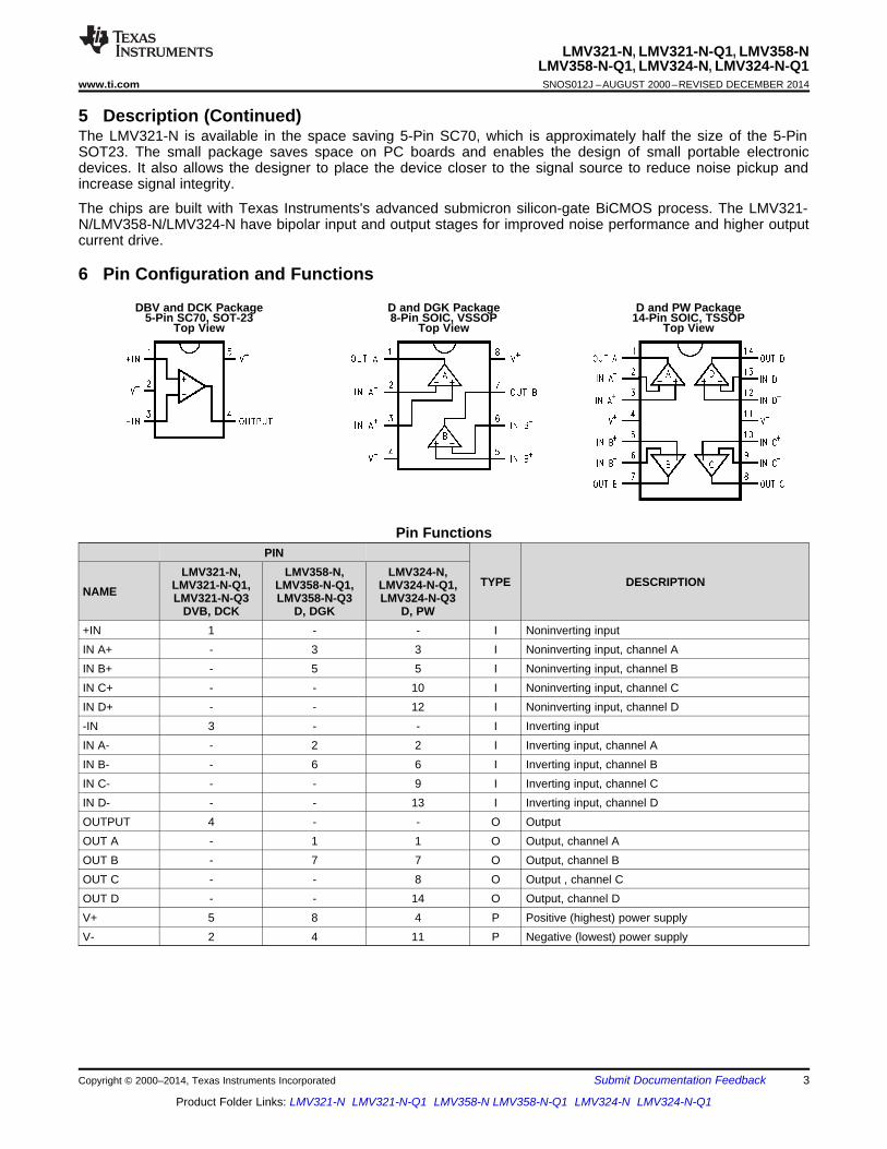
5 Description (Continued)The LMV321-N is available in the space saving 5-Pin SC70, which is approximately half the size of the 5-PinSOT23. The small package saves space on PC boards and enables the design of small portable electronicdevices. It also allows the designer to place the device closer to the signal source to reduce noise pickup andincrease signal integrity.
The chips are built with Texas Instruments's advanced submicron silicon-gate BiCMOS process. The LMV321-N/LMV358-N/LMV324-N have bipolar input and output stages for improved noise performance and higher outputcurrent drive.
6 Pin Configuration and Functions
DBV and DCK Package5-Pin SC70, SOT-23
Top View
D and DGK Package8-Pin SOIC, VSSOP
Top View
D and PW Package14-Pin SOIC, TSSOP
Top View
Pin FunctionsPIN
TYPE DESCRIPTIONNAME
LMV321-N,LMV321-N-Q1,LMV321-N-Q3
DVB, DCK
LMV358-N,LMV358-N-Q1,LMV358-N-Q3
D, DGK
LMV324-N,LMV324-N-Q1,LMV324-N-Q3
D, PW+IN 1 - - I Noninverting inputIN A+ - 3 3 I Noninverting input, channel AIN B+ - 5 5 I Noninverting input, channel BIN C+ - - 10 I Noninverting input, channel CIN D+ - - 12 I Noninverting input, channel D-IN 3 - - I Inverting inputIN A- - 2 2 I Inverting input, channel AIN B- - 6 6 I Inverting input, channel BIN C- - - 9 I Inverting input, channel CIN D- - - 13 I Inverting input, channel DOUTPUT 4 - - O OutputOUT A - 1 1 O Output, channel AOUT B - 7 7 O Output, channel BOUT C - - 8 O Output , channel COUT D - - 14 O Output, channel DV+ 5 8 4 P Positive (highest) power supplyV- 2 4 11 P Negative (lowest) power supply

4
LMV321-N, LMV321-N-Q1, LMV358-NLMV358-N-Q1, LMV324-N, LMV324-N-Q1SNOS012J –AUGUST 2000–REVISED DECEMBER 2014 www.ti.com
Product Folder Links: LMV321-N LMV321-N-Q1 LMV358-N LMV358-N-Q1 LMV324-N LMV324-N-Q1
Submit Documentation Feedback Copyright © 2000–2014, Texas Instruments Incorporated
(1) Absolute Maximum Ratings indicate limits beyond which damage to the device may occur. Recommended Operating Conditions indicateconditions for which the device is intended to be functional, but specific performance is not ensured. For ensured specifications and thetest conditions, see the Electrical Characteristics.
(2) If Military/Aerospace specified devices are required, please contact the Texas Instruments Sales Office / Distributors for availability andspecifications.
(3) Shorting output to V+ will adversely affect reliability.(4) Shorting output to V- will adversely affect reliability.(5) The maximum power dissipation is a function of TJ(MAX), RθJA. The maximum allowable power dissipation at any ambient temperature is
PD = (TJ(MAX) – TA)/ RθJA. All numbers apply for packages soldered directly onto a PC Board.
7 Specifications
7.1 Absolute Maximum RatingsSee (1) (2).
MIN MAX UNITDifferential Input Voltage ±Supply Voltage VInput Voltage −0.3 +Supply Voltage VSupply Voltage (V+–V −) 5.5 VOutput Short Circuit to V + (3)
Output Short Circuit to V − (4)
Soldering Information: Infrared or Convection (30 sec) 260 °CJunction Temperature (5) 150 °CStorage temperature Tstg −65 150 °C
(1) JEDEC document JEP155 states that 500-V HBM allows safe manufacturing with a standard ESD control process.
7.2 ESD Ratings - CommercialVALUE UNIT
LMV358-N, and LMV324-N in all packages
V(ESD) Electrostatic dischargeHuman-body model (HBM), per ANSI/ESDA/JEDEC JS-001 (1) ±2000
VMachine model ±100
LMV321-N in all packages
V(ESD) Electrostatic dischargeHuman-body model (HBM), per ANSI/ESDA/JEDEC JS-001 (1) ±900
VMachine model ±100
(1) AEC Q100-002 indicates that HBM stressing shall be in accordance with the ANSI/ESDA/JEDEC JS-001 specification.
7.3 ESD Ratings - AutomotiveVALUE UNIT
LMV358-N-Q1, LMV324-N-Q1, LMV358-N-Q3 and LMV324-N-Q3 in all packages
V(ESD) Electrostatic dischargeHuman-body model (HBM), per AEC Q100-002 (1) ±2000
VMachine model ±100
LM321-N-Q1 and LM321-N-Q3 in all packages
V(ESD) Electrostatic dischargeHuman-body model (HBM), per AEC Q100-002 (1) ±900
VMachine model ±100
(1) The maximum power dissipation is a function of TJ(MAX), RθJA. The maximum allowable power dissipation at any ambient temperature isPD = (TJ(MAX) – TA)/ RθJA. All numbers apply for packages soldered directly onto a PC Board.
7.4 Recommended Operating ConditionsMIN MAX UNIT
Supply Voltage 2.7 5.5 VTemperature Range (1): LMV321-N, LMV358-N, LMV324-N –40 125 °CTemperature Range (1): LMV321-N-Q1, LMV358-N-Q1, LMV324-N-Q1 –40 125 °CTemperature Range (1): LMV321-N-Q3, LMV358-N-Q3, LMV324-N-Q3 –40 85 °C

5
LMV321-N, LMV321-N-Q1, LMV358-NLMV358-N-Q1, LMV324-N, LMV324-N-Q1
www.ti.com SNOS012J –AUGUST 2000–REVISED DECEMBER 2014
Product Folder Links: LMV321-N LMV321-N-Q1 LMV358-N LMV358-N-Q1 LMV324-N LMV324-N-Q1
Submit Documentation FeedbackCopyright © 2000–2014, Texas Instruments Incorporated
(1) For more information about traditional and new thermal metrics, see the IC Package Thermal Metrics application report, SPRA953.
7.5 Thermal Information
THERMAL METRIC (1)
LMV321-N,LMV321-N-Q1,LMV321-N-Q3
LMV321-N LMV324-N,LMV324-N-Q1,LMV324-N-Q3
LMV358-N,LMV358-N-Q1,LMV358-N-Q3 UNIT
DBV DCK D PW D DGK5 PINS 14 PINS 8 PINS
RθJA Junction-to-ambient thermalresistance 265 478 145 155 190 235 °C/W
(1) All limits are ensured by testing or statistical analysis.(2) Typical values represent the most likely parametric norm as determined at the time of characterization. Actual typical values may vary
over time and will also depend on the application and configuration. The typical values are not tested and are not ensured on shippedproduction material.
7.6 2.7-V DC Electrical CharacteristicsUnless otherwise specified, all limits specified for TJ = 25°C, V+ = 2.7 V, V− = 0 V, VCM = 1.0 V, VO = V+/2 and RL > 1 MΩ.
TEST CONDITIONS MIN (1) TYP (2) MAX (1) UNITVOS Input Offset Voltage 1.7 7 mVTCVOS Input Offset Voltage Average Drift 5 µV/°CIB Input Bias Current 11 250 nAIOS Input Offset Current 5 50 nACMRR Common Mode Rejection Ratio 0 V ≤ VCM ≤ 1.7 V 50 63 dBPSRR Power Supply Rejection Ratio 2.7 V ≤ V+ ≤ 5 V
VO = 1V50 60 dB
VCM Input Common-Mode VoltageRange
For CMRR ≥ 50 dB 0 −0.2 V1.9 1.7 V
VO Output Swing RL = 10 kΩ to 1.35 V V+ −100 V+ −10 mV60 180 mV
IS Supply Current Single 80 170 µADualBoth amplifiers
140 340 µA
QuadAll four amplifiers
260 680 µA
(1) All limits are ensured by testing or statistical analysis.(2) Typical values represent the most likely parametric norm as determined at the time of characterization. Actual typical values may vary
over time and will also depend on the application and configuration. The typical values are not tested and are not ensured on shippedproduction material.
7.7 2.7-V AC Electrical CharacteristicsUnless otherwise specified, all limits specified for T J = 25°C, V+ = 2.7 V, V− = 0 V, VCM = 1.0 V, VO = V+/2 and RL > 1 MΩ.
TEST CONDITIONS MIN (1) TYP (2) MAX (1) UNITGBWP Gain-Bandwidth Product CL = 200 pF 1 MHzΦm Phase Margin 60 DegGm Gain Margin 10 dBen Input-Referred Voltage Noise f = 1 kHz 46
in Input-Referred Current Noise f = 1 kHz 0.17

6
LMV321-N, LMV321-N-Q1, LMV358-NLMV358-N-Q1, LMV324-N, LMV324-N-Q1SNOS012J –AUGUST 2000–REVISED DECEMBER 2014 www.ti.com
Product Folder Links: LMV321-N LMV321-N-Q1 LMV358-N LMV358-N-Q1 LMV324-N LMV324-N-Q1
Submit Documentation Feedback Copyright © 2000–2014, Texas Instruments Incorporated
(1) All limits are ensured by testing or statistical analysis.(2) Typical values represent the most likely parametric norm as determined at the time of characterization. Actual typical values may vary
over time and will also depend on the application and configuration. The typical values are not tested and are not ensured on shippedproduction material.
(3) RL is connected to V-. The output voltage is 0.5 V ≤ VO ≤ 4.5 V.
7.8 5-V DC Electrical CharacteristicsUnless otherwise specified, all limits specified for T J = 25°C, V+ = 5 V, V− = 0 V, VCM = 2.0 V, VO = V+/2 and R L > 1 MΩ.
TEST CONDITIONS MIN (1) TYP (2) MAX (1) UNITVOS Input Offset Voltage 1.7 7
mVOver Temperature 9
TCVOS Input Offset Voltage Average Drift 5 µV/°CIB Input Bias Current 15 250
nAOver Temperature 500
IOS Input Offset Current 5 50nA
Over Temperature 150CMRR Common Mode Rejection Ratio 0 V ≤ VCM ≤ 4 V 50 65 dBPSRR Power Supply Rejection Ratio 2.7 V ≤ V+ ≤ 5 V
VO = 1V, VCM = 1 V50 60 dB
VCM Input Common-Mode VoltageRange
For CMRR ≥ 50 dB 0 −0.2 V4.2 4 V
AV Large Signal Voltage Gain (3) RL = 2 kΩ 15 100V/mV
RL = 2 kΩ, Over Temperature 10VO Output Swing RL = 2 kΩ to 2.5 V V+ − 300 V+ −40
mV
RL = 2 kΩ to 2.5 V, Over Temperature V+ − 400RL = 2 kΩ to 2.5 V 120 300RL = 2 kΩ to 2.5 V, Over Temperature 400RL = 10 kΩ to 2.5 V V+ − 100 V+ − 10RL = 10 kΩ to 2.5 V, Over Temperature V+ − 200RL = 2 kΩ to 2.5 V 65 180RL = 2 kΩ to 2.5 V, 125°C 280
IO Output Short Circuit Current Sourcing, VO = 0 V 5 60mA
Sinking, VO = 5 V 10 160IS Supply Current Single 130 250
µA
Single, Over Temperature 350Dual (both amps) 210 440Dual (both amps), Over Temperature 615Quad (all four amps) 410 830Quad (all four amps), OverTemperature
1160

7
LMV321-N, LMV321-N-Q1, LMV358-NLMV358-N-Q1, LMV324-N, LMV324-N-Q1
www.ti.com SNOS012J –AUGUST 2000–REVISED DECEMBER 2014
Product Folder Links: LMV321-N LMV321-N-Q1 LMV358-N LMV358-N-Q1 LMV324-N LMV324-N-Q1
Submit Documentation FeedbackCopyright © 2000–2014, Texas Instruments Incorporated
(1) All limits are ensured by testing or statistical analysis.(2) Typical values represent the most likely parametric norm as determined at the time of characterization. Actual typical values may vary
over time and will also depend on the application and configuration. The typical values are not tested and are not ensured on shippedproduction material.
(3) Connected as voltage follower with 3-V step input. Number specified is the slower of the positive and negative slew rates.
7.9 5-V AC Electrical CharacteristicsUnless otherwise specified, all limits specified for TJ = 25°C, V+ = 5 V, V− = 0 V, VCM = 2.0 V, VO = V+/2 and R L > 1 MΩ.
TEST CONDITIONS MIN (1) TYP (2) MAX (1) UNITSR Slew Rate (3) 1 V/µsGBWP Gain-Bandwidth Product CL = 200 pF 1 MHzΦm Phase Margin 60 DegGm Gain Margin 10 dBen Input-Referred Voltage Noise f = 1 kHz 39
in Input-Referred Current Noise f = 1 kHz 0.21

8
LMV321-N, LMV321-N-Q1, LMV358-NLMV358-N-Q1, LMV324-N, LMV324-N-Q1SNOS012J –AUGUST 2000–REVISED DECEMBER 2014 www.ti.com
Product Folder Links: LMV321-N LMV321-N-Q1 LMV358-N LMV358-N-Q1 LMV324-N LMV324-N-Q1
Submit Documentation Feedback Copyright © 2000–2014, Texas Instruments Incorporated
7.10 Typical CharacteristicsUnless otherwise specified, VS = 5 V, single supply, TA = 25°C.
Figure 1. Supply Current vs. Supply Voltage (LMV321-N) Figure 2. Input Current vs. Temperature
Figure 3. Sourcing Current vs. Output Voltage Figure 4. Sourcing Current vs. Output Voltage
Figure 5. Sinking Current vs. Output Voltage Figure 6. Sinking Current vs. Output Voltage

9
LMV321-N, LMV321-N-Q1, LMV358-NLMV358-N-Q1, LMV324-N, LMV324-N-Q1
www.ti.com SNOS012J –AUGUST 2000–REVISED DECEMBER 2014
Product Folder Links: LMV321-N LMV321-N-Q1 LMV358-N LMV358-N-Q1 LMV324-N LMV324-N-Q1
Submit Documentation FeedbackCopyright © 2000–2014, Texas Instruments Incorporated
Typical Characteristics (continued)Unless otherwise specified, VS = 5 V, single supply, TA = 25°C.
Figure 7. Output Voltage Swing vs. Supply Voltage Figure 8. Input Voltage Noise vs. Frequency
Figure 9. Input Current Noise vs. Frequency Figure 10. Input Current Noise vs. Frequency
Figure 11. Crosstalk Rejection vs. Frequency Figure 12. PSRR vs. Frequency

10
LMV321-N, LMV321-N-Q1, LMV358-NLMV358-N-Q1, LMV324-N, LMV324-N-Q1SNOS012J –AUGUST 2000–REVISED DECEMBER 2014 www.ti.com
Product Folder Links: LMV321-N LMV321-N-Q1 LMV358-N LMV358-N-Q1 LMV324-N LMV324-N-Q1
Submit Documentation Feedback Copyright © 2000–2014, Texas Instruments Incorporated
Typical Characteristics (continued)Unless otherwise specified, VS = 5 V, single supply, TA = 25°C.
Figure 13. CMRR vs. Frequency Figure 14. CMRR vs. Input Common Mode Voltage
Figure 15. CMRR vs. Input Common Mode Voltage Figure 16. ΔVOS vs. CMR
Figure 17. ΔV OS vs. CMR Figure 18. Input Voltage vs. Output Voltage

11
LMV321-N, LMV321-N-Q1, LMV358-NLMV358-N-Q1, LMV324-N, LMV324-N-Q1
www.ti.com SNOS012J –AUGUST 2000–REVISED DECEMBER 2014
Product Folder Links: LMV321-N LMV321-N-Q1 LMV358-N LMV358-N-Q1 LMV324-N LMV324-N-Q1
Submit Documentation FeedbackCopyright © 2000–2014, Texas Instruments Incorporated
Typical Characteristics (continued)Unless otherwise specified, VS = 5 V, single supply, TA = 25°C.
Figure 19. Input Voltage vs. Output Voltage Figure 20. Open Loop Frequency Response
Figure 21. Open Loop Frequency Response Figure 22. Open Loop Frequency Response vs. Temperature
Figure 23. Gain and Phase vs. Capacitive Load Figure 24. Gain and Phase vs. Capacitive Load

12
LMV321-N, LMV321-N-Q1, LMV358-NLMV358-N-Q1, LMV324-N, LMV324-N-Q1SNOS012J –AUGUST 2000–REVISED DECEMBER 2014 www.ti.com
Product Folder Links: LMV321-N LMV321-N-Q1 LMV358-N LMV358-N-Q1 LMV324-N LMV324-N-Q1
Submit Documentation Feedback Copyright © 2000–2014, Texas Instruments Incorporated
Typical Characteristics (continued)Unless otherwise specified, VS = 5 V, single supply, TA = 25°C.
Figure 25. Slew Rate vs. Supply Voltage Figure 26. Non-Inverting Large Signal Pulse Response
Figure 27. Non-Inverting Large Signal Pulse Response Figure 28. Non-Inverting Large Signal Pulse Response
Figure 29. Non-Inverting Small Signal Pulse Response Figure 30. Non-Inverting Small Signal Pulse Response

13
LMV321-N, LMV321-N-Q1, LMV358-NLMV358-N-Q1, LMV324-N, LMV324-N-Q1
www.ti.com SNOS012J –AUGUST 2000–REVISED DECEMBER 2014
Product Folder Links: LMV321-N LMV321-N-Q1 LMV358-N LMV358-N-Q1 LMV324-N LMV324-N-Q1
Submit Documentation FeedbackCopyright © 2000–2014, Texas Instruments Incorporated
Typical Characteristics (continued)Unless otherwise specified, VS = 5 V, single supply, TA = 25°C.
Figure 31. Non-Inverting Small Signal Pulse Response Figure 32. Inverting Large Signal Pulse Response
Figure 33. Inverting Large Signal Pulse Response Figure 34. Inverting Large Signal Pulse Response
Figure 35. Inverting Small Signal Pulse Response Figure 36. Inverting Small Signal Pulse Response

14
LMV321-N, LMV321-N-Q1, LMV358-NLMV358-N-Q1, LMV324-N, LMV324-N-Q1SNOS012J –AUGUST 2000–REVISED DECEMBER 2014 www.ti.com
Product Folder Links: LMV321-N LMV321-N-Q1 LMV358-N LMV358-N-Q1 LMV324-N LMV324-N-Q1
Submit Documentation Feedback Copyright © 2000–2014, Texas Instruments Incorporated
Typical Characteristics (continued)Unless otherwise specified, VS = 5 V, single supply, TA = 25°C.
Figure 37. Inverting Small Signal Pulse ResponseFigure 38. Stability vs. Capacitive Load
Figure 39. Stability vs. Capacitive Load Figure 40. Stability vs. Capacitive Load
Figure 41. Stability vs. Capacitive Load Figure 42. THD vs. Frequency

15
LMV321-N, LMV321-N-Q1, LMV358-NLMV358-N-Q1, LMV324-N, LMV324-N-Q1
www.ti.com SNOS012J –AUGUST 2000–REVISED DECEMBER 2014
Product Folder Links: LMV321-N LMV321-N-Q1 LMV358-N LMV358-N-Q1 LMV324-N LMV324-N-Q1
Submit Documentation FeedbackCopyright © 2000–2014, Texas Instruments Incorporated
Typical Characteristics (continued)Unless otherwise specified, VS = 5 V, single supply, TA = 25°C.
Figure 43. Open Loop Output Impedance vs. Frequency Figure 44. Short Circuit Current vs. Temperature (Sinking)
Figure 45. Short Circuit Current vs. Temperature (Sourcing)

16
LMV321-N, LMV321-N-Q1, LMV358-NLMV358-N-Q1, LMV324-N, LMV324-N-Q1SNOS012J –AUGUST 2000–REVISED DECEMBER 2014 www.ti.com
Product Folder Links: LMV321-N LMV321-N-Q1 LMV358-N LMV358-N-Q1 LMV324-N LMV324-N-Q1
Submit Documentation Feedback Copyright © 2000–2014, Texas Instruments Incorporated
8 Detailed Description
8.1 OverviewThe LMV358-N/LMV324-N are low voltage (2.7 V to 5.5 V) versions of the dual and quad commodity op ampsLM358/LM324 (5 V to 30 V). The LMV321-N is the single channel version. The LMV321-N/LMV358-N/LMV324-Nare the most cost effective solutions for applications where low voltage operation, space efficiency, and low priceare important. They offer specifications that meet or exceed the familiar LM358/LM324. The LMV321-N/LMV358-N/LMV324-N have rail-to-rail output swing capability and the input common-mode voltage range includes ground.They all exhibit excellent speed to power ratio, achieving 1 MHz of bandwidth and 1-V/µs slew rate with lowsupply current.
8.1.1 Benefits of the LMV321-N/LMV358-N/LMV324-N
8.1.1.1 SizeThe small footprints of the LMV321-N/LMV358-N/LMV324-N packages save space on printed circuit boards, andenable the design of smaller electronic products, such as cellular phones, pagers, or other portable systems. Thelow profile of the LMV321-N/LMV358-N/LMV324-N make them possible to use in PCMCIA type III cards.
8.1.1.2 Signal IntegritySignals can pick up noise between the signal source and the amplifier. By using a physically smaller amplifierpackage, the LMV321-N/LMV358-N/LMV324-N can be placed closer to the signal source, reducing noise pickupand increasing signal integrity.
8.1.1.3 Simplified Board LayoutThese products help you to avoid using long PC traces in your PC board layout. This means that no additionalcomponents, such as capacitors and resistors, are needed to filter out the unwanted signals due to theinterference between the long PC traces.
8.1.1.4 Low Supply CurrentThese devices will help you to maximize battery life. They are ideal for battery powered systems.
8.1.1.5 Low Supply VoltageTexas Instruments provides ensured performance at 2.7 V and 5 V. These specifications ensure operationthroughout the battery lifetime.
8.1.1.6 Rail-to-Rail OutputRail-to-rail output swing provides maximum possible dynamic range at the output. This is particularly importantwhen operating on low supply voltages.
8.1.1.7 Input Includes GroundAllows direct sensing near GND in single supply operation.
Protection should be provided to prevent the input voltages from going negative more than −0.3V (at 25°C). Aninput clamp diode with a resistor to the IC input terminal can be used.
8.1.1.8 Ease of Use and Crossover DistortionThe LMV321-N/LMV358-N/LMV324-N offer specifications similar to the familiar LM324-N. In addition, the newLMV321-N/LMV358-N/LMV324-N effectively eliminate the output crossover distortion. The scope photos inFigure 46 and Figure 47 compare the output swing of the LMV324-N and the LM324-N in a voltage followerconfiguration, with VS = ± 2.5V and RL (= 2 kΩ) connected to GND. It is apparent that the crossover distortionhas been eliminated in the new LMV324-N.

_
+OUT
V+
V–
IN –
IN +
Copyright © 2016,Texas Instruments Incorporated
17
LMV321-N, LMV321-N-Q1, LMV358-NLMV358-N-Q1, LMV324-N, LMV324-N-Q1
www.ti.com SNOS012J –AUGUST 2000–REVISED DECEMBER 2014
Product Folder Links: LMV321-N LMV321-N-Q1 LMV358-N LMV358-N-Q1 LMV324-N LMV324-N-Q1
Submit Documentation FeedbackCopyright © 2000–2014, Texas Instruments Incorporated
Overview (continued)
Figure 46. Output Swing of LMV324 Figure 47. Output Swing of LM324
8.2 Functional Block Diagram
Figure 48. Each Amplifier
8.3 Feature Description
8.3.1 Capacitive Load ToleranceThe LMV321-N/LMV358-N/LMV324-N can directly drive 200 pF in unity-gain without oscillation. The unity-gainfollower is the most sensitive configuration to capacitive loading. Direct capacitive loading reduces the phasemargin of amplifiers. The combination of the amplifier's output impedance and the capacitive load induces phaselag. This results in either an underdamped pulse response or oscillation. To drive a heavier capacitive load, thecircuit in Figure 49 can be used.
Figure 49. Indirectly Driving a Capacitive Load Using Resistive Isolation
In Figure 49 , the isolation resistor RISO and the load capacitor CL form a pole to increase stability by adding morephase margin to the overall system. The desired performance depends on the value of RISO. The bigger the RISOresistor value, the more stable VOUT will be. Figure 50 is an output waveform of Figure 49 using 620Ω for RISOand 510 pF for CL..

18
LMV321-N, LMV321-N-Q1, LMV358-NLMV358-N-Q1, LMV324-N, LMV324-N-Q1SNOS012J –AUGUST 2000–REVISED DECEMBER 2014 www.ti.com
Product Folder Links: LMV321-N LMV321-N-Q1 LMV358-N LMV358-N-Q1 LMV324-N LMV324-N-Q1
Submit Documentation Feedback Copyright © 2000–2014, Texas Instruments Incorporated
Feature Description (continued)
Figure 50. Pulse Response of the LMV324 Circuit in Figure 49
The circuit in Figure 51 is an improvement to the one in Figure 49 because it provides DC accuracy as well asAC stability. If there were a load resistor in Figure 49, the output would be voltage divided by RISO and the loadresistor. Instead, in Figure 51, RF provides the DC accuracy by using feed-forward techniques to connect VIN toRL. Caution is needed in choosing the value of RF due to the input bias current of theLMV321-N/LMV358-N/LMV324-N. CF and RISO serve to counteract the loss of phase margin by feeding the high frequencycomponent of the output signal back to the amplifier's inverting input, thereby preserving phase margin in theoverall feedback loop. Increased capacitive drive is possible by increasing the value of CF . This in turn will slowdown the pulse response.
Figure 51. Indirectly Driving A Capacitive Load with DC Accuracy
8.3.2 Input Bias Current CancellationThe LMV321-N/LMV358-N/LMV324-N family has a bipolar input stage. The typical input bias current of LMV321-N/LMV358-N/LMV324-N is 15 nA with 5V supply. Thus a 100 kΩ input resistor will cause 1.5 mV of error voltage.By balancing the resistor values at both inverting and non-inverting inputs, the error caused by the amplifier'sinput bias current will be reduced. The circuit in Figure 52 shows how to cancel the error caused by input biascurrent.

19
LMV321-N, LMV321-N-Q1, LMV358-NLMV358-N-Q1, LMV324-N, LMV324-N-Q1
www.ti.com SNOS012J –AUGUST 2000–REVISED DECEMBER 2014
Product Folder Links: LMV321-N LMV321-N-Q1 LMV358-N LMV358-N-Q1 LMV324-N LMV324-N-Q1
Submit Documentation FeedbackCopyright © 2000–2014, Texas Instruments Incorporated
Feature Description (continued)
Figure 52. Cancelling the Error Caused by Input Bias Current
8.4 Device Functional ModesThe LMV321-N/LMV321-N-Q1/LMV358-N/LMV358-N-Q1/LMV324-N/LMV324-N-Q1 are powered on when thesupply is connected. They can be operated as a single supply or a dual supply operational amplifier dependingon the application.
20
LMV321-N, LMV321-N-Q1, LMV358-NLMV358-N-Q1, LMV324-N, LMV324-N-Q1SNOS012J –AUGUST 2000–REVISED DECEMBER 2014 www.ti.com
Product Folder Links: LMV321-N LMV321-N-Q1 LMV358-N LMV358-N-Q1 LMV324-N LMV324-N-Q1
Submit Documentation Feedback Copyright © 2000–2014, Texas Instruments Incorporated
9 Application and Implementation
NOTEInformation in the following applications sections is not part of the TI componentspecification, and TI does not warrant its accuracy or completeness. TI’s customers areresponsible for determining suitability of components for their purposes. Customers shouldvalidate and test their design implementation to confirm system functionality.
9.1 Application InformationThe LMV32x-N family of amplifiers is specified for operation from 2.7 V to 5 V (±1.35 V to ±2.5 V). Many of thespecifications apply from –40°C to 125°C. They provide ground-sensing inputs as well as rail-to-rail output swing.Parameters that can exhibit significant variance with regard to operating voltage or temperature are presented inthe Typical Characteristics.
9.2 Typical Applications
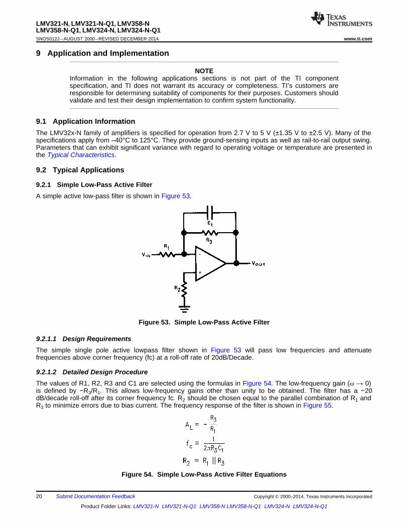
9.2.1 Simple Low-Pass Active FilterA simple active low-pass filter is shown in Figure 53.
Figure 53. Simple Low-Pass Active Filter
9.2.1.1 Design RequirementsThe simple single pole active lowpass filter shown in Figure 53 will pass low frequencies and attenuatefrequencies above corner frequency (fc) at a roll-off rate of 20dB/Decade.
9.2.1.2 Detailed Design ProcedureThe values of R1, R2, R3 and C1 are selected using the formulas in Figure 54. The low-frequency gain (ω → 0)is defined by −R3/R1. This allows low-frequency gains other than unity to be obtained. The filter has a −20dB/decade roll-off after its corner frequency fc. R2 should be chosen equal to the parallel combination of R1 andR3 to minimize errors due to bias current. The frequency response of the filter is shown in Figure 55.
Figure 54. Simple Low-Pass Active Filter Equations

21
LMV321-N, LMV321-N-Q1, LMV358-NLMV358-N-Q1, LMV324-N, LMV324-N-Q1
www.ti.com SNOS012J –AUGUST 2000–REVISED DECEMBER 2014
Product Folder Links: LMV321-N LMV321-N-Q1 LMV358-N LMV358-N-Q1 LMV324-N LMV324-N-Q1
Submit Documentation FeedbackCopyright © 2000–2014, Texas Instruments Incorporated
Typical Applications (continued)9.2.1.3 Application Curves
Figure 55. Frequency Response of Simple Low-Pass Active Filter
Note that the single-op-amp active filters are used in the applications that require low quality factor, Q( ≤ 10), lowfrequency (≤ 5 kHz), and low gain (≤ 10), or a small value for the product of gain times Q (≤ 100). The op ampshould have an open loop voltage gain at the highest frequency of interest at least 50 times larger than the gainof the filter at this frequency. In addition, the selected op amp should have a slew rate that meets the followingrequirement:
Slew Rate ≥ 0.5 × (ω HVOPP) × 10−6 V/µsec (1)
where ωH is the highest frequency of interest, and VOPP is the output peak-to-peak voltage.
9.2.2 Difference AmplifierThe difference amplifier allows the subtraction of two voltages or, as a special case, the cancellation of a signalcommon to two inputs. It is useful as a computational amplifier, in making a differential to single-endedconversion or in rejecting a common mode signal.
Figure 56. Difference Amplifier
9.2.3 Instrumentation CircuitsThe input impedance of the previous difference amplifier is set by the resistors R1, R2, R3, and R4. To eliminatethe problems of low input impedance, one way is to use a voltage follower ahead of each input as shown in thefollowing two instrumentation amplifiers.

22
LMV321-N, LMV321-N-Q1, LMV358-NLMV358-N-Q1, LMV324-N, LMV324-N-Q1SNOS012J –AUGUST 2000–REVISED DECEMBER 2014 www.ti.com
Product Folder Links: LMV321-N LMV321-N-Q1 LMV358-N LMV358-N-Q1 LMV324-N LMV324-N-Q1
Submit Documentation Feedback Copyright © 2000–2014, Texas Instruments Incorporated
Typical Applications (continued)9.2.3.1 Three-Op-Amp Instrumentation AmplifierThe quad LMV324 can be used to build a three-op-amp instrumentation amplifier as shown in Figure 57.
Figure 57. Three-Op-Amp Instrumentation Amplifier
The first stage of this instrumentation amplifier is a differential-input, differential-output amplifier, with two voltagefollowers. These two voltage followers assure that the input impedance is over 100 MΩ. The gain of thisinstrumentation amplifier is set by the ratio of R2/R1. R3 should equal R1, and R4 equal R2. Matching of R3 to R1and R4 to R2 affects the CMRR. For good CMRR over temperature, low drift resistors should be used. Making R4slightly smaller than R2 and adding a trim pot equal to twice the difference between R2 and R4 will allow theCMRR to be adjusted for optimum performance.
9.2.3.2 Two-Op-Amp Instrumentation AmplifierA two-op-amp instrumentation amplifier can also be used to make a high-input-impedance DC differentialamplifier (Figure 58). As in the three-op-amp circuit, this instrumentation amplifier requires precise resistormatching for good CMRR. R4 should equal R1 and, R3 should equal R2.
Figure 58. Two-Op-Amp Instrumentation Amplifier

23
LMV321-N, LMV321-N-Q1, LMV358-NLMV358-N-Q1, LMV324-N, LMV324-N-Q1
www.ti.com SNOS012J –AUGUST 2000–REVISED DECEMBER 2014
Product Folder Links: LMV321-N LMV321-N-Q1 LMV358-N LMV358-N-Q1 LMV324-N LMV324-N-Q1
Submit Documentation FeedbackCopyright © 2000–2014, Texas Instruments Incorporated
Typical Applications (continued)9.2.3.3 Single-Supply Inverting AmplifierThere may be cases where the input signal going into the amplifier is negative. Because the amplifier isoperating in single supply voltage, a voltage divider using R3 and R4 is implemented to bias the amplifier so theinput signal is within the input common-mode voltage range of the amplifier. The capacitor C1 is placed betweenthe inverting input and resistor R1 to block the DC signal going into the AC signal source, VIN. The values of R1and C1 affect the cutoff frequency, fc = 1/2πR1C1.
As a result, the output signal is centered around mid-supply (if the voltage divider provides V+/2 at the non-inverting input). The output can swing to both rails, maximizing the signal-to-noise ratio in a low voltage system.
Figure 59. Single-Supply Inverting Amplifier
9.2.4 Sallen-Key 2nd-Order Active Low-Pass FilterThe Sallen-Key 2nd-order active low-pass filter is illustrated in Figure 60. The DC gain of the filter is expressedas
(2)
Its transfer function is
(3)
Figure 60. Sallen-Key 2nd-Order Active Low-Pass Filter

24
LMV321-N, LMV321-N-Q1, LMV358-NLMV358-N-Q1, LMV324-N, LMV324-N-Q1SNOS012J –AUGUST 2000–REVISED DECEMBER 2014 www.ti.com
Product Folder Links: LMV321-N LMV321-N-Q1 LMV358-N LMV358-N-Q1 LMV324-N LMV324-N-Q1
Submit Documentation Feedback Copyright © 2000–2014, Texas Instruments Incorporated
Typical Applications (continued)9.2.4.1 Detailed Design ProcedureThe following paragraphs explain how to select values for R1, R2, R3, R4, C1, and C 2 for given filter requirements,such as ALP, Q, and fc.
The standard form for a 2nd-order low pass filter is
(4)
where
Q: Pole Quality Factor
ωC: Corner Frequency
A comparison between Equation 3 and Equation 4 yields
(5)
(6)
To reduce the required calculations in filter design, it is convenient to introduce normalization into thecomponents and design parameters. To normalize, let ωC = ωn = 1 rad/s, and C1 = C2 = Cn = 1F, and substitutethese values into Equation 5 and Equation 6. From Equation 5, we obtain
(7)
From Equation 6, we obtain
(8)
For minimum DC offset, V+ = V−, the resistor values at both inverting and non-inverting inputs should be equal,which means
(9)
From Equation 2 and Equation 9, we obtain
(10)
(11)
The values of C1 and C2 are normally close to or equal to
(12)
As a design example:
Require: ALP = 2, Q = 1, fc = 1 kHz
Start by selecting C1 and C2. Choose a standard value that is close to
(13)
(14)

25
LMV321-N, LMV321-N-Q1, LMV358-NLMV358-N-Q1, LMV324-N, LMV324-N-Q1
www.ti.com SNOS012J –AUGUST 2000–REVISED DECEMBER 2014
Product Folder Links: LMV321-N LMV321-N-Q1 LMV358-N LMV358-N-Q1 LMV324-N LMV324-N-Q1
Submit Documentation FeedbackCopyright © 2000–2014, Texas Instruments Incorporated
Typical Applications (continued)From Equation 7, Equation 8, Equation 10, and Equation 11,
R1= 1Ω (15)R2= 1Ω (16)R3= 4Ω (17)R4= 4Ω (18)
The above resistor values are normalized values with ωn = 1 rad/s and C1 = C2 = Cn = 1F. To scale thenormalized cutoff frequency and resistances to the real values, two scaling factors are introduced, frequencyscaling factor (kf) and impedance scaling factor (km).
(19)
Scaled values:R2 = R1 = 15.9 kΩ (20)R3 = R4 = 63.6 kΩ (21)C1 = C2 = 0.01 µF (22)
An adjustment to the scaling may be made in order to have realistic values for resistors and capacitors. Theactual value used for each component is shown in the circuit.
9.2.5 2nd-Order High Pass FilterA 2nd-order high pass filter can be built by simply interchanging those frequency selective components (R1, R2,C1, C2) in the Sallen-Key 2nd-order active low pass filter. As shown in Figure 61, resistors become capacitors,and capacitors become resistors. The resulted high pass filter has the same corner frequency and the samemaximum gain as the previous 2nd-order low pass filter if the same components are chosen.
Figure 61. Sallen-Key 2nd-Order Active High-Pass Filter
9.2.6 State Variable FilterA state variable filter requires three op amps. One convenient way to build state variable filters is with a quad opamp, such as the LMV324 (Figure 62).

26
LMV321-N, LMV321-N-Q1, LMV358-NLMV358-N-Q1, LMV324-N, LMV324-N-Q1SNOS012J –AUGUST 2000–REVISED DECEMBER 2014 www.ti.com
Product Folder Links: LMV321-N LMV321-N-Q1 LMV358-N LMV358-N-Q1 LMV324-N LMV324-N-Q1
Submit Documentation Feedback Copyright © 2000–2014, Texas Instruments Incorporated
Typical Applications (continued)This circuit can simultaneously represent a low-pass filter, high-pass filter, and bandpass filter at three differentoutputs. The equations for these functions are listed below. It is also called "Bi-Quad" active filter as it canproduce a transfer function which is quadratic in both numerator and denominator.
Figure 62. State Variable Active Filter
(23)
where for all three filters,
(24)
(25)
9.2.6.1 Detailed Design ProcedureAssume the system design requires a bandpass filter with f O = 1 kHz and Q = 50. What needs to be calculatedare capacitor and resistor values.
First choose convenient values for C1, R1 and R2:C1 = 1200 pF (26)

27
LMV321-N, LMV321-N-Q1, LMV358-NLMV358-N-Q1, LMV324-N, LMV324-N-Q1
www.ti.com SNOS012J –AUGUST 2000–REVISED DECEMBER 2014
Product Folder Links: LMV321-N LMV321-N-Q1 LMV358-N LMV358-N-Q1 LMV324-N LMV324-N-Q1
Submit Documentation FeedbackCopyright © 2000–2014, Texas Instruments Incorporated
Typical Applications (continued)2R2 = R1 = 30 kΩ (27)
Then from Equation 24,
(28)
From Equation 25,
(29)
From the above calculated values, the midband gain is H0 = R3/R2 = 100 (40 dB). The nearest 5% standardvalues have been added to Figure 62.
9.2.7 Pulse Generators and OscillatorsA pulse generator is shown in Figure 63. Two diodes have been used to separate the charge and dischargepaths to capacitor C.
Figure 63. Pulse Generator
When the output voltage VO is first at its high, VOH, the capacitor C is charged toward VOH through R2. Thevoltage across C rises exponentially with a time constant τ = R2C, and this voltage is applied to the invertinginput of the op amp. Meanwhile, the voltage at the non-inverting input is set at the positive threshold voltage(VTH+) of the generator. The capacitor voltage continually increases until it reaches VTH+, at which point theoutput of the generator will switch to its low, VOL which 0V is in this case. The voltage at the non-inverting input isswitched to the negative threshold voltage (VTH−) of the generator. The capacitor then starts to discharge towardVOL exponentially through R1, with a time constant τ = R1C. When the capacitor voltage reaches VTH−, the outputof the pulse generator switches to VOH. The capacitor starts to charge, and the cycle repeats itself.

28
LMV321-N, LMV321-N-Q1, LMV358-NLMV358-N-Q1, LMV324-N, LMV324-N-Q1SNOS012J –AUGUST 2000–REVISED DECEMBER 2014 www.ti.com
Product Folder Links: LMV321-N LMV321-N-Q1 LMV358-N LMV358-N-Q1 LMV324-N LMV324-N-Q1
Submit Documentation Feedback Copyright © 2000–2014, Texas Instruments Incorporated
Typical Applications (continued)
Figure 64. Waveforms of the Circuit in Figure 16
As shown in the waveforms in Figure 64, the pulse width (T1) is set by R2, C and VOH, and the time betweenpulses (T2) is set by R1, C and VOL. This pulse generator can be made to have different frequencies and pulsewidth by selecting different capacitor value and resistor values.
Figure 65 shows another pulse generator, with separate charge and discharge paths. The capacitor is chargedthrough R1 and is discharged through R2.

29
LMV321-N, LMV321-N-Q1, LMV358-NLMV358-N-Q1, LMV324-N, LMV324-N-Q1
www.ti.com SNOS012J –AUGUST 2000–REVISED DECEMBER 2014
Product Folder Links: LMV321-N LMV321-N-Q1 LMV358-N LMV358-N-Q1 LMV324-N LMV324-N-Q1
Submit Documentation FeedbackCopyright © 2000–2014, Texas Instruments Incorporated
Typical Applications (continued)
Figure 65. Pulse Generator
Figure 66 is a squarewave generator with the same path for charging and discharging the capacitor.
Figure 66. Squarewave Generator
9.2.8 Current Source and SinkThe LMV321-N/LMV358-N/LMV324-N can be used in feedback loops which regulate the current in external PNPtransistors to provide current sources or in external NPN transistors to provide current sinks.
9.2.8.1 Fixed Current SourceA multiple fixed current source is shown in Figure 67. A voltage (VREF = 2V) is established across resistor R3 bythe voltage divider (R3 and R4). Negative feedback is used to cause the voltage drop across R1 to be equal toVREF. This controls the emitter current of transistor Q1 and if we neglect the base current of Q1 and Q2,essentially this same current is available out of the collector of Q1.
Large input resistors can be used to reduce current loss and a Darlington connection can be used to reduceerrors due to the β of Q1.
The resistor, R2, can be used to scale the collector current of Q2 either above or below the 1 mA reference value.

30
LMV321-N, LMV321-N-Q1, LMV358-NLMV358-N-Q1, LMV324-N, LMV324-N-Q1SNOS012J –AUGUST 2000–REVISED DECEMBER 2014 www.ti.com
Product Folder Links: LMV321-N LMV321-N-Q1 LMV358-N LMV358-N-Q1 LMV324-N LMV324-N-Q1
Submit Documentation Feedback Copyright © 2000–2014, Texas Instruments Incorporated
Typical Applications (continued)
Figure 67. Fixed Current Source
9.2.8.2 High Compliance Current SinkA current sink circuit is shown in Figure 68. The circuit requires only one resistor (RE) and supplies an outputcurrent which is directly proportional to this resistor value.
Figure 68. High Compliance Current Sink

31
LMV321-N, LMV321-N-Q1, LMV358-NLMV358-N-Q1, LMV324-N, LMV324-N-Q1
www.ti.com SNOS012J –AUGUST 2000–REVISED DECEMBER 2014
Product Folder Links: LMV321-N LMV321-N-Q1 LMV358-N LMV358-N-Q1 LMV324-N LMV324-N-Q1
Submit Documentation FeedbackCopyright © 2000–2014, Texas Instruments Incorporated
Typical Applications (continued)9.2.9 Power AmplifierA power amplifier is illustrated in Figure 69. This circuit can provide a higher output current because a transistorfollower is added to the output of the op amp.
Figure 69. Power Amplifier
9.2.10 LED DriverThe LMV321-N/LMV358-N/LMV324-N can be used to drive an LED as shown in Figure 70.
Figure 70. LED Driver
9.2.11 Comparator With HysteresisThe LMV321-N/LMV358-N/LMV324-N can be used as a low power comparator. Figure 71 shows a comparatorwith hysteresis. The hysteresis is determined by the ratio of the two resistors.
VTH+ = VREF/(1+R 1/R2)+VOH/(1+R2/R1) (30)VTH− = VREF/(1+R 1/R2)+VOL/(1+R2/R1) (31)VH = (VOH−VOL)/(1+R 2/R1) (32)
where
VTH+: Positive Threshold Voltage
VTH−: Negative Threshold Voltage
VOH: Output Voltage at High
VOL: Output Voltage at Low
VH: Hysteresis Voltage
Since LMV321-N/LMV358-N/LMV324-N have rail-to-rail output, the (VOH−VOL) is equal to VS, which is the supplyvoltage.
VH = VS/(1+R2/R1) (33)

32
LMV321-N, LMV321-N-Q1, LMV358-NLMV358-N-Q1, LMV324-N, LMV324-N-Q1SNOS012J –AUGUST 2000–REVISED DECEMBER 2014 www.ti.com
Product Folder Links: LMV321-N LMV321-N-Q1 LMV358-N LMV358-N-Q1 LMV324-N LMV324-N-Q1
Submit Documentation Feedback Copyright © 2000–2014, Texas Instruments Incorporated
Typical Applications (continued)The differential voltage at the input of the op amp should not exceed the specified absolute maximum ratings.For real comparators that are much faster, we recommend you use Texas Instruments'sLMV331/LMV93/LMV339, which are single, dual and quad general purpose comparators for low voltageoperation.
Figure 71. Comparator with Hysteresis
10 Power Supply RecommendationsThe LMV3xx-N is specified for operation from 2.7 V to 5.5 V; many specifications apply from –40°C to 125°C.Parameters that can exhibit significant variance with regard to operating voltage or temperature are presented inthe Typical Characteristics.
Place 0.1-μF bypass capacitors close to the power-supply pins to reduce errors coupling in from noisy or highimpedance power supplies. For more detailed information on bypass capacitor placement, refer to the LayoutGuidelines section.
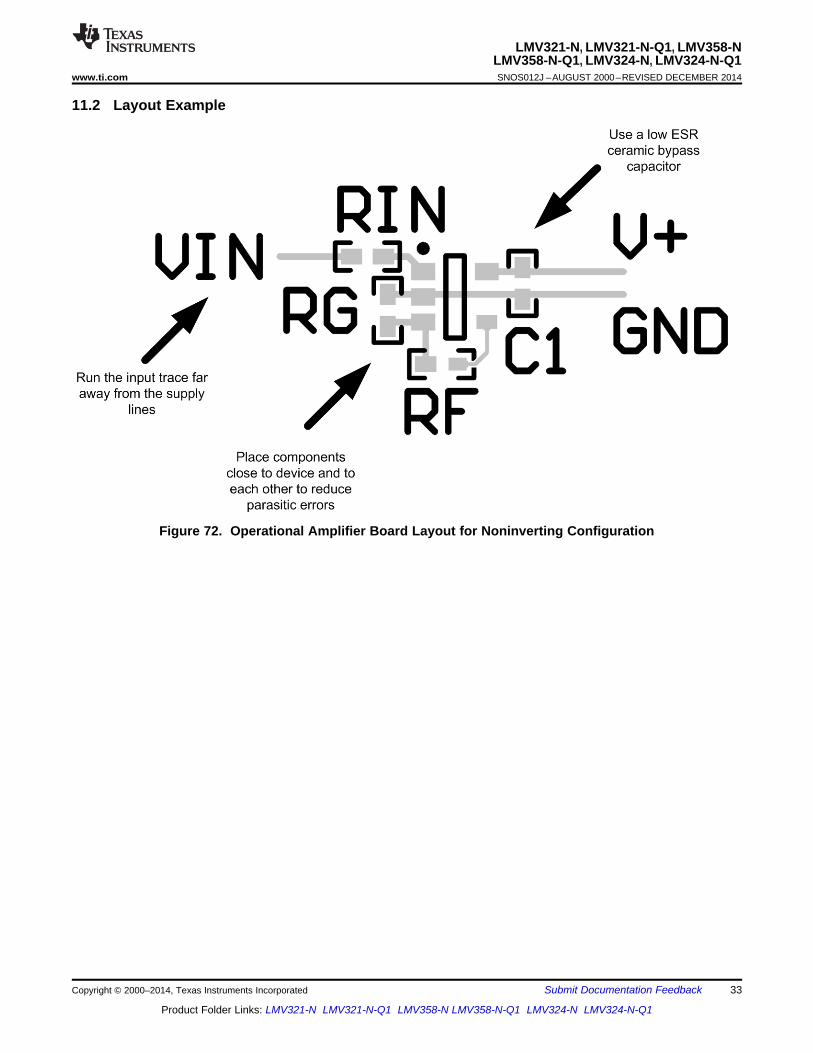
11 Layout
11.1 Layout GuidelinesFor best operational performance of the device, use good PCB layout practices, including:• Noise can propagate into analog circuitry through the power pins of the circuit as a whole and the operational
amplifier. Bypass capacitors are used to reduce the coupled noise by providing low impedance powersources local to the analog circuitry.– Connect low-ESR, 0.1-μF ceramic bypass capacitors between each supply pin and ground, placed as
close to the device as possible. A single bypass capacitor from V+ to ground is applicable for singlesupply applications.
• Separate grounding for analog and digital portions of circuitry is one of the simplest and most-effectivemethods of noise suppression. One or more layers on multilayer PCBs are usually devoted to ground planes.A ground plane helps distribute heat and reduces EMI noise pickup. Make sure to physically separate digitaland analog grounds, paying attention to the flow of the ground current. For more detailed information, refer toCircuit Board Layout Techniques, SLOA089.
• To reduce parasitic coupling, run the input traces as far away from the supply or output traces as possible. Ifit is not possible to keep them separate, it is much better to cross the sensitive trace perpendicular asopposed to in parallel with the noisy trace.
• Place the external components as close to the device as possible. Keeping RF and RG close to the invertinginput minimizes parasitic capacitance, as shown in Layout Example.
• Keep the length of input traces as short as possible. Always remember that the input traces are the mostsensitive part of the circuit.
• Consider a driven, low-impedance guard ring around the critical traces. A guard ring can significantly reduceleakage currents from nearby traces that are at different potentials.
33
LMV321-N, LMV321-N-Q1, LMV358-NLMV358-N-Q1, LMV324-N, LMV324-N-Q1
www.ti.com SNOS012J –AUGUST 2000–REVISED DECEMBER 2014
Product Folder Links: LMV321-N LMV321-N-Q1 LMV358-N LMV358-N-Q1 LMV324-N LMV324-N-Q1
Submit Documentation FeedbackCopyright © 2000–2014, Texas Instruments Incorporated
11.2 Layout Example
Figure 72. Operational Amplifier Board Layout for Noninverting Configuration

34
LMV321-N, LMV321-N-Q1, LMV358-NLMV358-N-Q1, LMV324-N, LMV324-N-Q1SNOS012J –AUGUST 2000–REVISED DECEMBER 2014 www.ti.com
Product Folder Links: LMV321-N LMV321-N-Q1 LMV358-N LMV358-N-Q1 LMV324-N LMV324-N-Q1
Submit Documentation Feedback Copyright © 2000–2014, Texas Instruments Incorporated
12 Device and Documentation Support
12.1 Related LinksThe table below lists quick access links. Categories include technical documents, support and communityresources, tools and software, and quick access to sample or buy.
Table 1. Related Links
PARTS PRODUCT FOLDER SAMPLE & BUY TECHNICALDOCUMENTS
TOOLS &SOFTWARE
SUPPORT &COMMUNITY
LMV321-N Click here Click here Click here Click here Click hereLMV321-N-Q1 Click here Click here Click here Click here Click here
LMV358-N Click here Click here Click here Click here Click hereLMV358-N-Q1 Click here Click here Click here Click here Click here
LMV324-N Click here Click here Click here Click here Click hereLMV324-N-Q1 Click here Click here Click here Click here Click here
12.2 TrademarksAll trademarks are the property of their respective owners.
12.3 Electrostatic Discharge CautionThese devices have limited built-in ESD protection. The leads should be shorted together or the device placed in conductive foamduring storage or handling to prevent electrostatic damage to the MOS gates.
12.4 GlossarySLYZ022 — TI Glossary.
This glossary lists and explains terms, acronyms, and definitions.
13 Mechanical, Packaging, and Orderable InformationThe following pages include mechanical, packaging, and orderable information. This information is the mostcurrent data available for the designated devices. This data is subject to change without notice and revision ofthis document. For browser-based versions of this data sheet, refer to the left-hand navigation.

PACKAGE OPTION ADDENDUM
www.ti.com 19-Dec-2017
Addendum-Page 1
PACKAGING INFORMATION
Orderable Device Status(1)
Package Type PackageDrawing
Pins PackageQty
Eco Plan(2)
Lead/Ball Finish(6)
MSL Peak Temp(3)
Op Temp (°C) Device Marking(4/5)
Samples
LMV321M5 NRND SOT-23 DBV 5 1000 TBD Call TI Call TI -40 to 125 A13
LMV321M5/NOPB ACTIVE SOT-23 DBV 5 1000 Green (RoHS& no Sb/Br)
CU SN Level-1-260C-UNLIM -40 to 125 A13
LMV321M5X/NOPB ACTIVE SOT-23 DBV 5 3000 Green (RoHS& no Sb/Br)
CU SN Level-1-260C-UNLIM -40 to 125 A13
LMV321M7 NRND SC70 DCK 5 1000 TBD Call TI Call TI -40 to 125 A12
LMV321M7/NOPB ACTIVE SC70 DCK 5 1000 Green (RoHS& no Sb/Br)
CU SN Level-1-260C-UNLIM -40 to 125 A12
LMV321M7X NRND SC70 DCK 5 3000 TBD Call TI Call TI -40 to 125 A12
LMV321M7X/NOPB ACTIVE SC70 DCK 5 3000 Green (RoHS& no Sb/Br)
CU SN Level-1-260C-UNLIM -40 to 125 A12
LMV321Q1M5/NOPB ACTIVE SOT-23 DBV 5 1000 Green (RoHS& no Sb/Br)
CU SN Level-1-260C-UNLIM -40 to 125 AYA
LMV321Q1M5X/NOPB ACTIVE SOT-23 DBV 5 3000 Green (RoHS& no Sb/Br)
CU SN Level-1-260C-UNLIM -40 to 125 AYA
LMV321Q3M5/NOPB ACTIVE SOT-23 DBV 5 1000 Green (RoHS& no Sb/Br)
CU SN Level-1-260C-UNLIM -40 to 85 AZA
LMV321Q3M5X/NOPB ACTIVE SOT-23 DBV 5 3000 Green (RoHS& no Sb/Br)
CU SN Level-1-260C-UNLIM -40 to 85 AZA
LMV324M NRND SOIC D 14 55 TBD Call TI Call TI -40 to 125 LMV324M
LMV324M/NOPB ACTIVE SOIC D 14 55 Green (RoHS& no Sb/Br)
CU SN Level-1-260C-UNLIM -40 to 125 LMV324M
LMV324MT/NOPB ACTIVE TSSOP PW 14 94 Green (RoHS& no Sb/Br)
CU NIPDAU | CU SN Level-1-260C-UNLIM -40 to 125 LMV324MT
LMV324MTX NRND TSSOP PW 14 2500 TBD Call TI Call TI -40 to 125 LMV324MT
LMV324MTX/NOPB ACTIVE TSSOP PW 14 2500 Green (RoHS& no Sb/Br)
CU NIPDAU | CU SN Level-1-260C-UNLIM -40 to 125 LMV324MT
LMV324MX NRND SOIC D 14 2500 TBD Call TI Call TI -40 to 125 LMV324M
LMV324MX/NOPB ACTIVE SOIC D 14 2500 Green (RoHS& no Sb/Br)
CU SN Level-1-260C-UNLIM -40 to 125 LMV324M
LMV324Q1MA/NOPB ACTIVE SOIC D 14 55 Green (RoHS& no Sb/Br)
CU SN Level-1-260C-UNLIM -40 to 125 LMV324Q1MA

PACKAGE OPTION ADDENDUM
www.ti.com 19-Dec-2017
Addendum-Page 2
Orderable Device Status(1)
Package Type PackageDrawing
Pins PackageQty
Eco Plan(2)
Lead/Ball Finish(6)
MSL Peak Temp(3)
Op Temp (°C) Device Marking(4/5)
Samples
LMV324Q1MAX/NOPB ACTIVE SOIC D 14 2500 Green (RoHS& no Sb/Br)
CU SN Level-1-260C-UNLIM -40 to 125 LMV324Q1MA
LMV324Q1MT/NOPB ACTIVE TSSOP PW 14 94 Green (RoHS& no Sb/Br)
CU SN Level-1-260C-UNLIM -40 to 125 LMV324Q1MT
LMV324Q1MTX/NOPB ACTIVE TSSOP PW 14 2500 Green (RoHS& no Sb/Br)
CU SN Level-1-260C-UNLIM -40 to 125 LMV324Q1MT
LMV324Q3MA/NOPB ACTIVE SOIC D 14 55 Green (RoHS& no Sb/Br)
CU SN Level-1-260C-UNLIM -40 to 85 LMV324Q3MA
LMV324Q3MAX/NOPB ACTIVE SOIC D 14 2500 Green (RoHS& no Sb/Br)
CU SN Level-1-260C-UNLIM -40 to 85 LMV324Q3MA
LMV324Q3MT/NOPB ACTIVE TSSOP PW 14 94 Green (RoHS& no Sb/Br)
CU SN Level-1-260C-UNLIM -40 to 85 LMV324Q3MT
LMV324Q3MTX/NOPB ACTIVE TSSOP PW 14 2500 Green (RoHS& no Sb/Br)
CU SN Level-1-260C-UNLIM -40 to 85 LMV324Q3MT
LMV358M NRND SOIC D 8 95 TBD Call TI Call TI -40 to 125 LMV358M
LMV358M/NOPB ACTIVE SOIC D 8 95 Green (RoHS& no Sb/Br)
CU SN Level-1-260C-UNLIM -40 to 125 LMV358M
LMV358MM NRND VSSOP DGK 8 1000 TBD Call TI Call TI -40 to 125 V358
LMV358MM/NOPB ACTIVE VSSOP DGK 8 1000 Green (RoHS& no Sb/Br)
CU SN Level-1-260C-UNLIM -40 to 125 V358
LMV358MMX/NOPB ACTIVE VSSOP DGK 8 3500 Green (RoHS& no Sb/Br)
CU SN Level-1-260C-UNLIM -40 to 125 V358
LMV358MX NRND SOIC D 8 2500 TBD Call TI Call TI -40 to 125 LMV358M
LMV358MX/NOPB ACTIVE SOIC D 8 2500 Green (RoHS& no Sb/Br)
CU SN Level-1-260C-UNLIM -40 to 125 LMV358M
LMV358Q1MA/NOPB ACTIVE SOIC D 8 95 Green (RoHS& no Sb/Br)
CU SN Level-1-260C-UNLIM -40 to 125 LMV358Q1MA
LMV358Q1MAX/NOPB ACTIVE SOIC D 8 2500 Green (RoHS& no Sb/Br)
CU SN Level-1-260C-UNLIM -40 to 125 LMV358Q1MA
LMV358Q1MM/NOPB ACTIVE VSSOP DGK 8 1000 Green (RoHS& no Sb/Br)
CU SN Level-1-260C-UNLIM -40 to 125 AFAA
LMV358Q1MMX/NOPB ACTIVE VSSOP DGK 8 3500 Green (RoHS& no Sb/Br)
CU SN Level-1-260C-UNLIM -40 to 125 AFAA

PACKAGE OPTION ADDENDUM
www.ti.com 19-Dec-2017
Addendum-Page 3
Orderable Device Status(1)
Package Type PackageDrawing
Pins PackageQty
Eco Plan(2)
Lead/Ball Finish(6)
MSL Peak Temp(3)
Op Temp (°C) Device Marking(4/5)
Samples
LMV358Q3MA/NOPB ACTIVE SOIC D 8 95 Green (RoHS& no Sb/Br)
CU SN Level-1-260C-UNLIM -40 to 85 LMV358Q3MA
LMV358Q3MAX/NOPB ACTIVE SOIC D 8 2500 Green (RoHS& no Sb/Br)
CU SN Level-1-260C-UNLIM -40 to 85 LMV358Q3MA
LMV358Q3MM/NOPB ACTIVE VSSOP DGK 8 1000 Green (RoHS& no Sb/Br)
CU SN Level-1-260C-UNLIM -40 to 85 AHAA
LMV358Q3MMX/NOPB ACTIVE VSSOP DGK 8 3500 Green (RoHS& no Sb/Br)
CU SN Level-1-260C-UNLIM -40 to 85 AHAA
(1) The marketing status values are defined as follows:ACTIVE: Product device recommended for new designs.LIFEBUY: TI has announced that the device will be discontinued, and a lifetime-buy period is in effect.NRND: Not recommended for new designs. Device is in production to support existing customers, but TI does not recommend using this part in a new design.PREVIEW: Device has been announced but is not in production. Samples may or may not be available.OBSOLETE: TI has discontinued the production of the device.
(2) RoHS: TI defines "RoHS" to mean semiconductor products that are compliant with the current EU RoHS requirements for all 10 RoHS substances, including the requirement that RoHS substancedo not exceed 0.1% by weight in homogeneous materials. Where designed to be soldered at high temperatures, "RoHS" products are suitable for use in specified lead-free processes. TI mayreference these types of products as "Pb-Free".RoHS Exempt: TI defines "RoHS Exempt" to mean products that contain lead but are compliant with EU RoHS pursuant to a specific EU RoHS exemption.Green: TI defines "Green" to mean the content of Chlorine (Cl) and Bromine (Br) based flame retardants meet JS709B low halogen requirements of <=1000ppm threshold. Antimony trioxide basedflame retardants must also meet the <=1000ppm threshold requirement.
(3) MSL, Peak Temp. - The Moisture Sensitivity Level rating according to the JEDEC industry standard classifications, and peak solder temperature.
(4) There may be additional marking, which relates to the logo, the lot trace code information, or the environmental category on the device.
(5) Multiple Device Markings will be inside parentheses. Only one Device Marking contained in parentheses and separated by a "~" will appear on a device. If a line is indented then it is a continuationof the previous line and the two combined represent the entire Device Marking for that device.
(6) Lead/Ball Finish - Orderable Devices may have multiple material finish options. Finish options are separated by a vertical ruled line. Lead/Ball Finish values may wrap to two lines if the finishvalue exceeds the maximum column width.
Important Information and Disclaimer:The information provided on this page represents TI's knowledge and belief as of the date that it is provided. TI bases its knowledge and belief on informationprovided by third parties, and makes no representation or warranty as to the accuracy of such information. Efforts are underway to better integrate information from third parties. TI has taken andcontinues to take reasonable steps to provide representative and accurate information but may not have conducted destructive testing or chemical analysis on incoming materials and chemicals.TI and TI suppliers consider certain information to be proprietary, and thus CAS numbers and other limited information may not be available for release.

PACKAGE OPTION ADDENDUM
www.ti.com 19-Dec-2017
Addendum-Page 4
In no event shall TI's liability arising out of such information exceed the total purchase price of the TI part(s) at issue in this document sold by TI to Customer on an annual basis.
OTHER QUALIFIED VERSIONS OF LMV321-N, LMV321-N-Q1, LMV324-N, LMV324-N-Q1, LMV358-N, LMV358-N-Q1 :
• Catalog: LMV321-N, LMV324-N, LMV358-N
• Automotive: LMV321-N-Q1, LMV324-N-Q1, LMV358-N-Q1
NOTE: Qualified Version Definitions:
• Catalog - TI's standard catalog product
• Automotive - Q100 devices qualified for high-reliability automotive applications targeting zero defects
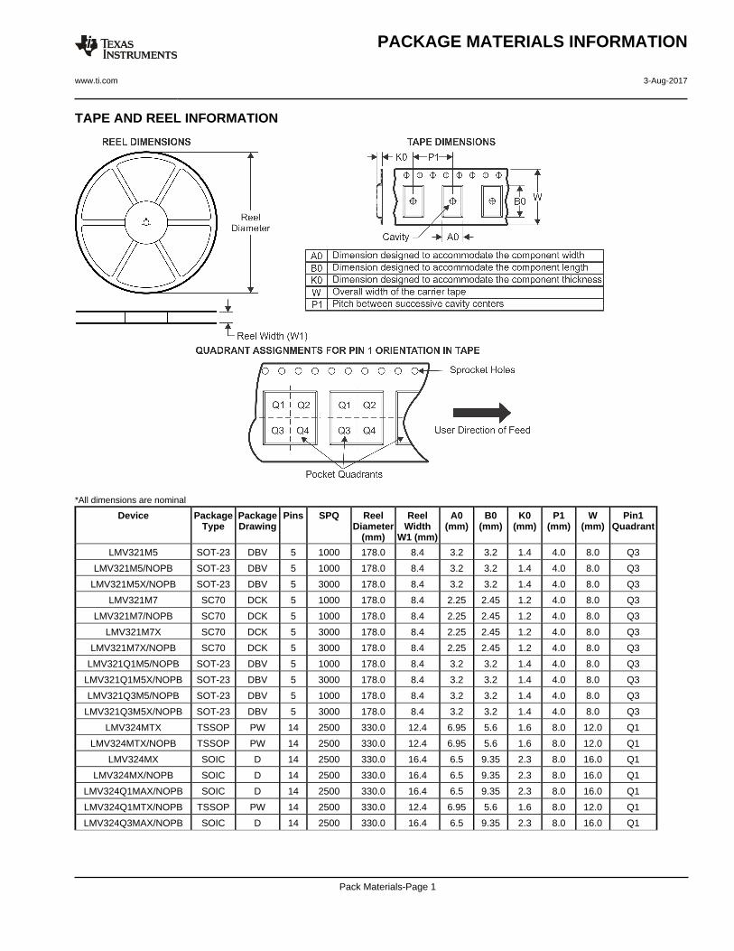
TAPE AND REEL INFORMATION
*All dimensions are nominal
Device PackageType
PackageDrawing
Pins SPQ ReelDiameter
(mm)
ReelWidth
W1 (mm)
A0(mm)
B0(mm)
K0(mm)
P1(mm)
W(mm)
Pin1Quadrant
LMV321M5 SOT-23 DBV 5 1000 178.0 8.4 3.2 3.2 1.4 4.0 8.0 Q3
LMV321M5/NOPB SOT-23 DBV 5 1000 178.0 8.4 3.2 3.2 1.4 4.0 8.0 Q3
LMV321M5X/NOPB SOT-23 DBV 5 3000 178.0 8.4 3.2 3.2 1.4 4.0 8.0 Q3
LMV321M7 SC70 DCK 5 1000 178.0 8.4 2.25 2.45 1.2 4.0 8.0 Q3
LMV321M7/NOPB SC70 DCK 5 1000 178.0 8.4 2.25 2.45 1.2 4.0 8.0 Q3
LMV321M7X SC70 DCK 5 3000 178.0 8.4 2.25 2.45 1.2 4.0 8.0 Q3
LMV321M7X/NOPB SC70 DCK 5 3000 178.0 8.4 2.25 2.45 1.2 4.0 8.0 Q3
LMV321Q1M5/NOPB SOT-23 DBV 5 1000 178.0 8.4 3.2 3.2 1.4 4.0 8.0 Q3
LMV321Q1M5X/NOPB SOT-23 DBV 5 3000 178.0 8.4 3.2 3.2 1.4 4.0 8.0 Q3
LMV321Q3M5/NOPB SOT-23 DBV 5 1000 178.0 8.4 3.2 3.2 1.4 4.0 8.0 Q3
LMV321Q3M5X/NOPB SOT-23 DBV 5 3000 178.0 8.4 3.2 3.2 1.4 4.0 8.0 Q3
LMV324MTX TSSOP PW 14 2500 330.0 12.4 6.95 5.6 1.6 8.0 12.0 Q1
LMV324MTX/NOPB TSSOP PW 14 2500 330.0 12.4 6.95 5.6 1.6 8.0 12.0 Q1
LMV324MX SOIC D 14 2500 330.0 16.4 6.5 9.35 2.3 8.0 16.0 Q1
LMV324MX/NOPB SOIC D 14 2500 330.0 16.4 6.5 9.35 2.3 8.0 16.0 Q1
LMV324Q1MAX/NOPB SOIC D 14 2500 330.0 16.4 6.5 9.35 2.3 8.0 16.0 Q1
LMV324Q1MTX/NOPB TSSOP PW 14 2500 330.0 12.4 6.95 5.6 1.6 8.0 12.0 Q1
LMV324Q3MAX/NOPB SOIC D 14 2500 330.0 16.4 6.5 9.35 2.3 8.0 16.0 Q1
PACKAGE MATERIALS INFORMATION
www.ti.com 3-Aug-2017
Pack Materials-Page 1

Device PackageType
PackageDrawing
Pins SPQ ReelDiameter
(mm)
ReelWidth
W1 (mm)
A0(mm)
B0(mm)
K0(mm)
P1(mm)
W(mm)
Pin1Quadrant
LMV324Q3MTX/NOPB TSSOP PW 14 2500 330.0 12.4 6.95 5.6 1.6 8.0 12.0 Q1
LMV358MM VSSOP DGK 8 1000 178.0 12.4 5.3 3.4 1.4 8.0 12.0 Q1
LMV358MM/NOPB VSSOP DGK 8 1000 178.0 12.4 5.3 3.4 1.4 8.0 12.0 Q1
LMV358MMX/NOPB VSSOP DGK 8 3500 330.0 12.4 5.3 3.4 1.4 8.0 12.0 Q1
LMV358MX SOIC D 8 2500 330.0 12.4 6.5 5.4 2.0 8.0 12.0 Q1
LMV358MX/NOPB SOIC D 8 2500 330.0 12.4 6.5 5.4 2.0 8.0 12.0 Q1
LMV358Q1MAX/NOPB SOIC D 8 2500 330.0 12.4 6.5 5.4 2.0 8.0 12.0 Q1
LMV358Q1MM/NOPB VSSOP DGK 8 1000 178.0 12.4 5.3 3.4 1.4 8.0 12.0 Q1
LMV358Q1MMX/NOPB VSSOP DGK 8 3500 330.0 12.4 5.3 3.4 1.4 8.0 12.0 Q1
LMV358Q3MAX/NOPB SOIC D 8 2500 330.0 12.4 6.5 5.4 2.0 8.0 12.0 Q1
LMV358Q3MM/NOPB VSSOP DGK 8 1000 178.0 12.4 5.3 3.4 1.4 8.0 12.0 Q1
LMV358Q3MMX/NOPB VSSOP DGK 8 3500 330.0 12.4 5.3 3.4 1.4 8.0 12.0 Q1
*All dimensions are nominal
Device Package Type Package Drawing Pins SPQ Length (mm) Width (mm) Height (mm)
LMV321M5 SOT-23 DBV 5 1000 210.0 185.0 35.0
LMV321M5/NOPB SOT-23 DBV 5 1000 210.0 185.0 35.0
LMV321M5X/NOPB SOT-23 DBV 5 3000 210.0 185.0 35.0
LMV321M7 SC70 DCK 5 1000 210.0 185.0 35.0
LMV321M7/NOPB SC70 DCK 5 1000 210.0 185.0 35.0
PACKAGE MATERIALS INFORMATION
www.ti.com 3-Aug-2017
Pack Materials-Page 2

Device Package Type Package Drawing Pins SPQ Length (mm) Width (mm) Height (mm)
LMV321M7X SC70 DCK 5 3000 210.0 185.0 35.0
LMV321M7X/NOPB SC70 DCK 5 3000 210.0 185.0 35.0
LMV321Q1M5/NOPB SOT-23 DBV 5 1000 210.0 185.0 35.0
LMV321Q1M5X/NOPB SOT-23 DBV 5 3000 210.0 185.0 35.0
LMV321Q3M5/NOPB SOT-23 DBV 5 1000 210.0 185.0 35.0
LMV321Q3M5X/NOPB SOT-23 DBV 5 3000 210.0 185.0 35.0
LMV324MTX TSSOP PW 14 2500 367.0 367.0 35.0
LMV324MTX/NOPB TSSOP PW 14 2500 367.0 367.0 35.0
LMV324MX SOIC D 14 2500 367.0 367.0 35.0
LMV324MX/NOPB SOIC D 14 2500 367.0 367.0 35.0
LMV324Q1MAX/NOPB SOIC D 14 2500 367.0 367.0 35.0
LMV324Q1MTX/NOPB TSSOP PW 14 2500 367.0 367.0 35.0
LMV324Q3MAX/NOPB SOIC D 14 2500 367.0 367.0 35.0
LMV324Q3MTX/NOPB TSSOP PW 14 2500 367.0 367.0 35.0
LMV358MM VSSOP DGK 8 1000 210.0 185.0 35.0
LMV358MM/NOPB VSSOP DGK 8 1000 210.0 185.0 35.0
LMV358MMX/NOPB VSSOP DGK 8 3500 367.0 367.0 35.0
LMV358MX SOIC D 8 2500 367.0 367.0 35.0
LMV358MX/NOPB SOIC D 8 2500 367.0 367.0 35.0
LMV358Q1MAX/NOPB SOIC D 8 2500 367.0 367.0 35.0
LMV358Q1MM/NOPB VSSOP DGK 8 1000 210.0 185.0 35.0
LMV358Q1MMX/NOPB VSSOP DGK 8 3500 367.0 367.0 35.0
LMV358Q3MAX/NOPB SOIC D 8 2500 367.0 367.0 35.0
LMV358Q3MM/NOPB VSSOP DGK 8 1000 210.0 185.0 35.0
LMV358Q3MMX/NOPB VSSOP DGK 8 3500 367.0 367.0 35.0
PACKAGE MATERIALS INFORMATION
www.ti.com 3-Aug-2017
Pack Materials-Page 3


www.ti.com
PACKAGE OUTLINE
C
TYP0.220.08
0.25
3.02.6
2X 0.95
1.9
1.45 MAX
TYP0.150.00
5X 0.50.3
TYP0.60.3
TYP80
1.9
A
3.052.75
B1.751.45
(1.1)
SOT-23 - 1.45 mm max heightDBV0005ASMALL OUTLINE TRANSISTOR
4214839/C 04/2017
NOTES: 1. All linear dimensions are in millimeters. Any dimensions in parenthesis are for reference only. Dimensioning and tolerancing per ASME Y14.5M.2. This drawing is subject to change without notice.3. Refernce JEDEC MO-178.
0.2 C A B
1
34
5
2
INDEX AREAPIN 1
GAGE PLANE
SEATING PLANE
0.1 C
SCALE 4.000

www.ti.com
EXAMPLE BOARD LAYOUT
0.07 MAXARROUND
0.07 MINARROUND
5X (1.1)
5X (0.6)
(2.6)
(1.9)
2X (0.95)
(R0.05) TYP
4214839/C 04/2017
SOT-23 - 1.45 mm max heightDBV0005ASMALL OUTLINE TRANSISTOR
NOTES: (continued) 4. Publication IPC-7351 may have alternate designs. 5. Solder mask tolerances between and around signal pads can vary based on board fabrication site.
SYMM
LAND PATTERN EXAMPLEEXPOSED METAL SHOWN
SCALE:15X
PKG
1
3 4
5
2
SOLDER MASKOPENINGMETAL UNDER
SOLDER MASK
SOLDER MASKDEFINED
EXPOSED METAL
METALSOLDER MASKOPENING
NON SOLDER MASKDEFINED
(PREFERRED)
SOLDER MASK DETAILS
EXPOSED METAL

www.ti.com
EXAMPLE STENCIL DESIGN
(2.6)
(1.9)
2X(0.95)
5X (1.1)
5X (0.6)
(R0.05) TYP
SOT-23 - 1.45 mm max heightDBV0005ASMALL OUTLINE TRANSISTOR
4214839/C 04/2017
NOTES: (continued) 6. Laser cutting apertures with trapezoidal walls and rounded corners may offer better paste release. IPC-7525 may have alternate design recommendations. 7. Board assembly site may have different recommendations for stencil design.
SOLDER PASTE EXAMPLEBASED ON 0.125 mm THICK STENCIL
SCALE:15X
SYMM
PKG
1
3 4
5
2


IMPORTANT NOTICE
Texas Instruments Incorporated (TI) reserves the right to make corrections, enhancements, improvements and other changes to itssemiconductor products and services per JESD46, latest issue, and to discontinue any product or service per JESD48, latest issue. Buyersshould obtain the latest relevant information before placing orders and should verify that such information is current and complete.TI’s published terms of sale for semiconductor products (http://www.ti.com/sc/docs/stdterms.htm) apply to the sale of packaged integratedcircuit products that TI has qualified and released to market. Additional terms may apply to the use or sale of other types of TI products andservices.Reproduction of significant portions of TI information in TI data sheets is permissible only if reproduction is without alteration and isaccompanied by all associated warranties, conditions, limitations, and notices. TI is not responsible or liable for such reproduceddocumentation. Information of third parties may be subject to additional restrictions. Resale of TI products or services with statementsdifferent from or beyond the parameters stated by TI for that product or service voids all express and any implied warranties for theassociated TI product or service and is an unfair and deceptive business practice. TI is not responsible or liable for any such statements.Buyers and others who are developing systems that incorporate TI products (collectively, “Designers”) understand and agree that Designersremain responsible for using their independent analysis, evaluation and judgment in designing their applications and that Designers havefull and exclusive responsibility to assure the safety of Designers' applications and compliance of their applications (and of all TI productsused in or for Designers’ applications) with all applicable regulations, laws and other applicable requirements. Designer represents that, withrespect to their applications, Designer has all the necessary expertise to create and implement safeguards that (1) anticipate dangerousconsequences of failures, (2) monitor failures and their consequences, and (3) lessen the likelihood of failures that might cause harm andtake appropriate actions. Designer agrees that prior to using or distributing any applications that include TI products, Designer willthoroughly test such applications and the functionality of such TI products as used in such applications.TI’s provision of technical, application or other design advice, quality characterization, reliability data or other services or information,including, but not limited to, reference designs and materials relating to evaluation modules, (collectively, “TI Resources”) are intended toassist designers who are developing applications that incorporate TI products; by downloading, accessing or using TI Resources in anyway, Designer (individually or, if Designer is acting on behalf of a company, Designer’s company) agrees to use any particular TI Resourcesolely for this purpose and subject to the terms of this Notice.TI’s provision of TI Resources does not expand or otherwise alter TI’s applicable published warranties or warranty disclaimers for TIproducts, and no additional obligations or liabilities arise from TI providing such TI Resources. TI reserves the right to make corrections,enhancements, improvements and other changes to its TI Resources. TI has not conducted any testing other than that specificallydescribed in the published documentation for a particular TI Resource.Designer is authorized to use, copy and modify any individual TI Resource only in connection with the development of applications thatinclude the TI product(s) identified in such TI Resource. NO OTHER LICENSE, EXPRESS OR IMPLIED, BY ESTOPPEL OR OTHERWISETO ANY OTHER TI INTELLECTUAL PROPERTY RIGHT, AND NO LICENSE TO ANY TECHNOLOGY OR INTELLECTUAL PROPERTYRIGHT OF TI OR ANY THIRD PARTY IS GRANTED HEREIN, including but not limited to any patent right, copyright, mask work right, orother intellectual property right relating to any combination, machine, or process in which TI products or services are used. Informationregarding or referencing third-party products or services does not constitute a license to use such products or services, or a warranty orendorsement thereof. Use of TI Resources may require a license from a third party under the patents or other intellectual property of thethird party, or a license from TI under the patents or other intellectual property of TI.TI RESOURCES ARE PROVIDED “AS IS” AND WITH ALL FAULTS. TI DISCLAIMS ALL OTHER WARRANTIES ORREPRESENTATIONS, EXPRESS OR IMPLIED, REGARDING RESOURCES OR USE THEREOF, INCLUDING BUT NOT LIMITED TOACCURACY OR COMPLETENESS, TITLE, ANY EPIDEMIC FAILURE WARRANTY AND ANY IMPLIED WARRANTIES OFMERCHANTABILITY, FITNESS FOR A PARTICULAR PURPOSE, AND NON-INFRINGEMENT OF ANY THIRD PARTY INTELLECTUALPROPERTY RIGHTS. TI SHALL NOT BE LIABLE FOR AND SHALL NOT DEFEND OR INDEMNIFY DESIGNER AGAINST ANY CLAIM,INCLUDING BUT NOT LIMITED TO ANY INFRINGEMENT CLAIM THAT RELATES TO OR IS BASED ON ANY COMBINATION OFPRODUCTS EVEN IF DESCRIBED IN TI RESOURCES OR OTHERWISE. IN NO EVENT SHALL TI BE LIABLE FOR ANY ACTUAL,DIRECT, SPECIAL, COLLATERAL, INDIRECT, PUNITIVE, INCIDENTAL, CONSEQUENTIAL OR EXEMPLARY DAMAGES INCONNECTION WITH OR ARISING OUT OF TI RESOURCES OR USE THEREOF, AND REGARDLESS OF WHETHER TI HAS BEENADVISED OF THE POSSIBILITY OF SUCH DAMAGES.Unless TI has explicitly designated an individual product as meeting the requirements of a particular industry standard (e.g., ISO/TS 16949and ISO 26262), TI is not responsible for any failure to meet such industry standard requirements.Where TI specifically promotes products as facilitating functional safety or as compliant with industry functional safety standards, suchproducts are intended to help enable customers to design and create their own applications that meet applicable functional safety standardsand requirements. Using products in an application does not by itself establish any safety features in the application. Designers mustensure compliance with safety-related requirements and standards applicable to their applications. Designer may not use any TI products inlife-critical medical equipment unless authorized officers of the parties have executed a special contract specifically governing such use.Life-critical medical equipment is medical equipment where failure of such equipment would cause serious bodily injury or death (e.g., lifesupport, pacemakers, defibrillators, heart pumps, neurostimulators, and implantables). Such equipment includes, without limitation, allmedical devices identified by the U.S. Food and Drug Administration as Class III devices and equivalent classifications outside the U.S.TI may expressly designate certain products as completing a particular qualification (e.g., Q100, Military Grade, or Enhanced Product).Designers agree that it has the necessary expertise to select the product with the appropriate qualification designation for their applicationsand that proper product selection is at Designers’ own risk. Designers are solely responsible for compliance with all legal and regulatoryrequirements in connection with such selection.Designer will fully indemnify TI and its representatives against any damages, costs, losses, and/or liabilities arising out of Designer’s non-compliance with the terms and provisions of this Notice.
Mailing Address: Texas Instruments, Post Office Box 655303, Dallas, Texas 75265Copyright © 2018, Texas Instruments Incorporated