lm95234 datasheet - ti.com · lm95234 snis136d – august 2006– revised march 2013 lm95234 quad...
TRANSCRIPT

LM95234
www.ti.com SNIS136D –AUGUST 2006–REVISED MARCH 2013
LM95234 Quad Remote Diode and Local Temperature Sensor with SMBus Interface andTruTherm™ Technology
Check for Samples: LM95234
1FEATURES – (e.g. Laptop, Desktop, Workstations,Server)
23• Accurately Senses Die Temperature of 4• Electronic Test EquipmentRemote ICs or Diode Junctions and Local
Temperature • Office Electronics• TruTherm BJT Beta Compensation Technology
DESCRIPTIONAccurately Senses Sub-micron ProcessLM95234 is an 11-bit digital temperature sensor withThermal Diodesa 2-wire System Management Bus (SMBus) interface• Programmable Digital Filters and Analog Frontthat can very accurately monitor the temperature ofEnd Filterfour remote diodes as well as its own temperature
• 0.125°C LSb Temperature Resolution that includes patent pending remote diodeTruTherm™ BJT beta compensation beta• 0.03125°C LSb Remote Temperaturecompensation technology. The four remote diodesResolution with Digital Filter Enabledcan be external devices such as microprocessors,• +127.875°C/–128°C and 0°C/255°C Remotegraphics processors or diode-connected 2N3904s.
Ranges The LM95234's TruTherm BJT beta compensation• Remote Diode Fault Detection, Model technology allows sensing of 90 nm or 65 nm process
Selection and Offset Correction thermal diodes accurately.• Mask and Status Register Support The LM95234 reports temperature in two different
formats for +127.875°C/–128°C range and 0°C/255°C• 3 Programmable TCRIT Outputs withrange. The LM95234 TCRIT1, TCRIT2 and TCRIT3Programmable Shared Hysteresis and Fault-outputs are triggered when any unmasked channelQueueexceeds its corresponding programmable limit and• Programmable Conversion Rate and Shutdown can be used to shutdown the system, to turn on the
Mode One-shot Conversion Control system fans or as a microcontroller interrupt function.• SMBus 2.0 Compatible Interface, Supports The current status of the TCRIT1, TCRIT2 and
TIMEOUT TCRIT3 pins can be read back from the statusregisters. Mask registers are available for further• Three-level Address Pincontrol of the TCRIT outputs.
• 14-pin WSON PackageTwo LM95234 remote temperature channels haveprogrammable digital filters while the other twoKEY SPECIFICATIONSremote channels utilize a fault-queue to minimize
• Local Temperature Accuracy ±2.0°C (max) unwanted TCRIT events when temperature spikesare encountered.• Remote Diode Temperature Accuracy ±0.875°C
(max) For optimum flexibility and accuracy, each LM95234• Supply Voltage 3.0V to 3.6V channel includes registers for sub-micron process or
2N3904 diode model selection as well as offset• Average Supply Current (1Hz conversion rate)correction. A three-level address pin allowsconnection of up to 3 LM95234s to the same SMBusAPPLICATIONSmaster. The LM95234 includes power saving
• Processor/Computer System Thermal functions such as: programmable conversion rate,Management shutdown mode, and disabling of unused channels.
1
Please be aware that an important notice concerning availability, standard warranty, and use in critical applications ofTexas Instruments semiconductor products and disclaimers thereto appears at the end of this data sheet.
2TruTherm is a trademark of Texas Instruments.3All other trademarks are the property of their respective owners.
PRODUCTION DATA information is current as of publication date. Copyright © 2006–2013, Texas Instruments IncorporatedProducts conform to specifications per the terms of the TexasInstruments standard warranty. Production processing does notnecessarily include testing of all parameters.

3.0V-3.6V
LM95234Local
Diode Selector'-6Converter
11-Bit or 10-Bit Plus Sign
Remote10-bit Plus Sign
Local
TruThermTM
TemperatureSensorCircuitry
Local Temperature
Registers
Limit, Statusand
MaskRegisters
Remote 1Digital Filter
Remote 1 Temperature
Registers
Remote 1 Offset Register
SMBus Interface
Remote 2 Digital Filter
Remote 2 Temperature
Registers
Remote 2 Offset Register
Remote 3 Status Fault
Queue
Remote 3 Temperature
Registers
Remote 3 Offset Register
Remote 4 Status Fault
Queue
Remote 4 Temperature
Registers
Remote 4 Offset Register
Conversion Rate Rgister
Diode Configuration
RegistersControl Logic
D-
RemoteDiode4 Selector
D4+
RemoteDiode3 Selector
D3+
RemoteDiode2 Selector
D2+
RemoteDiode1 Selector
D1+
General Configuration
Registers
T_CRITControlLogic
SMBCLK
SMBDAT
TCRIT3
TCRIT2
TCRIT1
LM95234
TCRIT3NC 141
VDD SMBCLK2 13
D4+ SMBDAT3 12
D3+ TCRIT24 11
D- TCRIT15 10
D2+ A06 9
D1+ GND7 8
LM95234
SNIS136D –AUGUST 2006–REVISED MARCH 2013 www.ti.com
Connection Diagram
Figure 1. WSON-14TOP VIEW
Simplified Block Diagram
2 Submit Documentation Feedback Copyright © 2006–2013, Texas Instruments Incorporated
Product Folder Links: LM95234

LM95234
www.ti.com SNIS136D –AUGUST 2006–REVISED MARCH 2013
PIN DESCRIPTIONSLabel Pin # Function Typical Connection
NC 1 No Connect Not connected. May be left floating, connected to GND or VDD.
VDD 2 Positive Supply Voltage Input DC Voltage from 3.0V to 3.6V. VDD should be bypassed with a0.1 µF capacitor in parallel with 100 pF. The 100 pF capacitorshould be placed as close as possible to the power supply pin.Noise should be kept below 200 mVp-p, a 10 µF capacitor maybe required to achieve this.
D4+ 3 Diode Current Source Fourth Diode Anode. Connected to remote discrete diode-connected transistor junction or to the diode-connectedtransistor junction on a remote IC whose die temperature isbeing sensed. A capacitor is not required between D4+ and D-.A 100 pF capacitor between D4+ and D- can be added andmay improve performance in noisy systems. Float this pin ifthis thermal diode is not used.
D3+ 4 Diode Current Source Third Diode Anode. Connected to remote discrete diode-connected transistor junction or to the diode-connectedtransistor junction on a remote IC whose die temperature isbeing sensed. A capacitor is not required between D3+ and D-.A 100 pF capacitor between D3+ and D- can be added andmay improve performance in noisy systems. Float this pin ifthis thermal diode is not used.
D− 5 Diode Return Current Sink All Diode Cathodes. Common D- pin for all four remote diodes.
D2+ 6 Diode Current Source Second Diode Anode. Connected to remote discrete diode-connected transistor junction or to the diode-connectedtransistor junction on a remote IC whose die temperature isbeing sensed. A capacitor is not required between D2+ and D-.A 100 pF capacitor between D2+ and D- can be added andmay improve performance in noisy systems. Float this pin ifthis thermal diode is not used.
D1+ 7 Diode Current Source First Diode Anode. Connected to remote discrete diode-connected transistor junction or to the diode-connectedtransistor junction on a remote IC whose die temperature isbeing sensed. A capacitor is not required between D1+ and D-.A 100 pF capacitor between D1+ and D- can be added andmay improve performance in noisy systems. Float this pin ifthis thermal diode is not used.
GND 8 Power Supply Ground System low noise ground.
A0 9 Digital Input SMBus slave address select pin. Selects one of threeaddresses. Can be tied to VDD, GND, or to the middle of aresistor divider connected between VDD and GND.
TCRIT1 10 Digital Output, Open-Drain Critical temperature output 1. Requires pull-up resistor. Active"LOW".
TCRIT2 11 Digital Output, Open-Drain Critical temperature output 2. Requires pull-up resistor. Active"LOW".
SMBDAT 12 SMBus Bidirectional Data Line, From and to Controller; may require an external pull-up resistorOpen-Drain Output
SMBCLK 13 SMBus Clock Input From Controller; may require an external pull-up resistor
TCRIT3 14 Digital Output, Open-Drain Critical temperature output 3. Requires pull-up resistor. Active"LOW".
Copyright © 2006–2013, Texas Instruments Incorporated Submit Documentation Feedback 3
Product Folder Links: LM95234

11
12
13
14
SMBus
Master
* Note, place close to LM95234 pins.
** Note, optional - place close to LM95234 pins.
LM95234
1
2
3
4
NC
VDDD4+
D3+
SMBCLK
C1*
100 pF
C20.1 PF
SMBCLK
SMBDAT
C7**
100 pF
+3.3V
Standby
R4
1.3k
R5
1.3k
D-
D2+
D1+
5
6
7 8
9
10
A0
SMBDAT
PROCESSOR
Q2
MMBT3904
Q1
MMBT3904
C6**
100 pF
C4**
100 pF
C5**
100 pF
R3
10k
R2
10k
R1
10k
SO
DIMM
HDD
GPU
C310 PF
TCRIT2
TCRIT1
TCRIT3
GND
LM95234
SNIS136D –AUGUST 2006–REVISED MARCH 2013 www.ti.com
Typical Application
These devices have limited built-in ESD protection. The leads should be shorted together or the device placed in conductive foamduring storage or handling to prevent electrostatic damage to the MOS gates.
Absolute Maximum Ratings (1)
Supply Voltage −0.3V to 6.0V
Voltage at SMBDAT, SMBCLK, TCRIT1, TCRIT2, TCRIT3 −0.5V to 6.0V
Voltage at Other Pins −0.3V to (VDD + 0.3V)
D− Input Current ±1 mA
Input Current at All Other Pins (2) ±5 mA
Package Input Current (2) 30 mA
SMBDAT, TCRIT1, TCRIT2, TCRIT3 Output Sink Current 10 mA
Storage Temperature −65°C to +150°C
ESD Susceptibility (3) Human Body Model 2000V
Machine Model 200V
Charge Device Model 1000V
Soldering process must comply with TI’s reflow temperature profile specifications. Refer to http://www.ti.com/packaging (4)
(1) Absolute Maximum Ratings indicate limits beyond which damage to the device may occur. DC and AC electrical specifications do notapply when operating the device beyond its rated operating conditions.
(2) When the input voltage (VI) at any pin exceeds the power supplies (VI < GND or VI > VDD), the current at that pin should be limited to 5mA. Parasitic components and or ESD protection circuitry are shown in Table 1 for the LM95234's pins.
(3) Human body model, 100 pF discharged through a 1.5 kΩ resistor. Machine model, 200 pF discharged directly into each pin. ChargedDevice Model (CDM) simulates a pin slowly acquiring charge (such as from a device sliding down the feeder in an automatedassembler) then rapidly being discharged.
(4) Reflow temperature profiles are different for packages containing lead (Pb) than for those that do not.
Operating RatingsOperating Temperature Range −40°C to +140°C
Electrical Characteristics Temperature Range TMIN ≤ TA ≤ TMAX
LM95234CISD −40°C ≤ TA ≤ +125°C
Supply Voltage Range (VDD) +3.0V to +3.6V
4 Submit Documentation Feedback Copyright © 2006–2013, Texas Instruments Incorporated
Product Folder Links: LM95234
LM95234
www.ti.com SNIS136D –AUGUST 2006–REVISED MARCH 2013
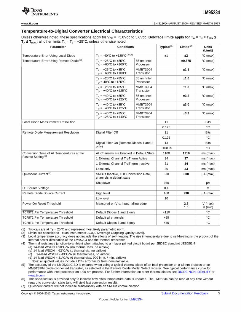
Temperature-to-Digital Converter Electrical CharacteristicsUnless otherwise noted, these specifications apply for VDD = +3.0Vdc to 3.6Vdc. Boldface limits apply for TA = TJ = TMIN ≤TA ≤ TMAX; all other limits TA = TJ = +25°C, unless otherwise noted.
Parameter Conditions Typical (1) Limits (2) Units(Limit)
Temperature Error Using Local Diode TA = -40°C to +125°C (3) (4) ±1 ±2 °C (max)
Temperature Error Using Remote Diode (5) TA = +25°C to +85°C 65 nm Intel ±0.875 °C (max)TD = +60°C to +100°C Processor
TA = +25°C to +85°C MMBT3904 ±1.1 °C (max)TD = +60°C to +100°C Transistor
TA = +25°C to +85°C 65 nm Intel ±1.0 °C (max)TD = 40°C to +125°C Processor
TA = +25°C to +85°C MMBT3904 ±1.3 °C (max)TD = −40°C to +125°C Transistor
TA = −40°C to +85°C 65 nm Intel ±3.2 °C (max)TD = −40°C to +125°C Processor
TA = −40°C to +85°C MMBT3904 ±3.0 °C (max)TD = −40°C to +125°C Transistor
TA = −40°C to +85°C MMBT3904 ±3.3 °C (max)TD = 125°C to +140°C Transistor
Local Diode Measurement Resolution 11 Bits
0.125 °C
Remote Diode Measurement Resolution Digital Filter Off 11 Bits
0.125 °C
Digital Filter On (Remote Diodes 1 and 2 13 Bitsonly) 0.03125 °C
Conversion Time of All Temperatures at the All Channels are Enabled in Default State 1100 1210 ms (max)Fastest Setting (6)
1 External Channel TruTherm Active 34 37 ms (max)
1 External Channel TruTherm Inactive 31 34 ms (max)
Local only 30 33 ms (max)
Quiescent Current (7) SMBus Inactive, 1Hz Conversion Rate, 570 800 µA (max)channels in default state
Shutdown 360 µA
D− Source Voltage 0.4 V
Remote Diode Source Current High level 160 230 µA (max)
Low level 10
Power-On Reset Threshold Measured on VDD input, falling edge 2.8 V (max)1.6 V (min)
TCRIT1 Pin Temperature Threshold Default Diodes 1 and 2 only +110 °C
TCRIT2 Pin Temperature Threshold Default all channels +85 °C
TCRIT3 Pin Temperature Threshold Default Diodes 3 and 4 only +85 °C
(1) Typicals are at TA = 25°C and represent most likely parametric norm.(2) Limits are specified to Texas Instruments' AOQL (Average Outgoing Quality Level).(3) Local temperature accuracy does not include the effects of self-heating. The rise in temperature due to self-heating is the product of the
internal power dissipation of the LM95234 and the thermal resistance.(4) Thermal resistance junction-to-ambient when attached to a 4 layer printed circuit board per JEDEC standard JESD51-7:
(a) 14-lead WSON = 90°C/W (no thermal vias, no airflow)(b) 14-lead WSON = 63°C/W (1 thermal via, no airflow)(c) 14-lead WSON = 43°C/W (6 thermal vias, no airflow)(d) 14-lead WSON = 31°C/W (6 thermal vias, 900 ln. ft. / min. airflow)
Note: all quoted values include +15% error factor from nominal value.(5) The accuracy of the LM95234CISD is ensured when using a typical thermal diode of an Intel processor on a 65 nm process or an
MMBT3904 diode-connected transistor, as selected in the Remote Diode Model Select register. See typical performance curve forperformance with Intel processor on a 90 nm process. For further information on other thermal diodes see DIODE NON-IDEALITY orwww.ti.com.
(6) This specification is provided only to indicate how often temperature data is updated. The LM95234 can be read at any time withoutregard to conversion state (and will yield last conversion result).
(7) Quiescent current will not increase substantially with an SMBus communication.
Copyright © 2006–2013, Texas Instruments Incorporated Submit Documentation Feedback 5
Product Folder Links: LM95234
LM95234
SNIS136D –AUGUST 2006–REVISED MARCH 2013 www.ti.com
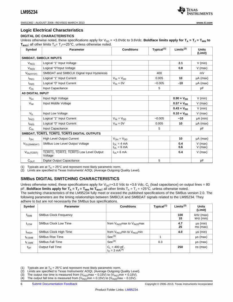
Logic Electrical CharacteristicsDIGITAL DC CHARACTERISTICSUnless otherwise noted, these specifications apply for VDD = +3.0Vdc to 3.6Vdc. Boldface limits apply for TA = TJ = TMIN toTMAX; all other limits TA= TJ=+25°C, unless otherwise noted.
Symbol Parameter Conditions Typical (1) Limits (2) Units(Limit)
SMBDAT, SMBCLK INPUTS
VIN(1) Logical “1” Input Voltage 2.1 V (min)
VIN(0) Logical “0”Input Voltage 0.8 V (max)
VIN(HYST) SMBDAT and SMBCLK Digital Input Hysteresis 400 mV
IIN(1) Logical “1” Input Current VIN = VDD 0.005 10 µA (max)
IIN(0) Logical “0” Input Current VIN = 0V −0.005 -10 µA (max)
CIN Input Capacitance 5 pF
A0 DIGITAL INPUT
VIH Input High Voltage 0.90 × VDD V (min)
VIM Input Middle Voltage 0.57 × VDD V (max)
0.43 × VDD V (min)
VIL Input Low Voltage 0.10 × VDD V (max)
IIN(1) Logical "1" Input Current VIN = VDD −0.005 −10 µA (min)
IIN(0) Logical "0" Input Current VIN = 0V 0.005 10 µA (max)
CIN Input Capacitance 5 pF
SMBDAT, TCRIT1, TCRIT2, TCRIT3 DIGITAL OUTPUTS
IOH High Level Output Current VOH = VDD 10 µA (max)
VOL(SMBDAT) SMBus Low Level Output Voltage IOL = 4 mA 0.4 V (max)IOL = 6 mA 0.6 V (max)
VOL(TCRIT) TCRIT1, TCRIT2, TCRIT3 Low Level Output IOL= 6 mA 0.4 V (max)Voltage
COUT Digital Output Capacitance 5 pF
(1) Typicals are at TA = 25°C and represent most likely parametric norm.(2) Limits are specified to Texas Instruments' AOQL (Average Outgoing Quality Level).
SMBus DIGITAL SWITCHING CHARACTERISTICSUnless otherwise noted, these specifications apply for VDD=+3.0 Vdc to +3.6 Vdc, CL (load capacitance) on output lines = 80pF. Boldface limits apply for TA = TJ = TMIN to TMAX; all other limits TA = TJ = +25°C, unless otherwise noted.The switching characteristics of the LM95234 fully meet or exceed the published specifications of the SMBus version 2.0. Thefollowing parameters are the timing relationships between SMBCLK and SMBDAT signals related to the LM95234. Theyadhere to but are not necessarily the SMBus bus specifications.
Symbol Parameter Conditions Typical (1) Limits (2) Units(Limit)
fSMB SMBus Clock Frequency 100 kHz (max)10 kHz (min)
tLOW SMBus Clock Low Time from VIN(0)max to VIN(0)max 4.7 µs (min)25 ms (max)
tHIGH SMBus Clock High Time from VIN(1)min to VIN(1)min 4.0 µs (min)
tR,SMB SMBus Rise Time See (3) 1 µs (max)
tF,SMB SMBus Fall Time See (4) 0.3 µs (max)
tOF Output Fall Time CL = 400 pF, 250 ns (max)IO = 3 mA (4)
(1) Typicals are at TA = 25°C and represent most likely parametric norm.(2) Limits are specified to Texas Instruments' AOQL (Average Outgoing Quality Level).(3) The output rise time is measured from (VIN(0)max − 0.15V) to (VIN(1)min + 0.15V).(4) The output fall time is measured from (VIN(1)min + 0.15V) to (VIN(0)max − 0.15V).
6 Submit Documentation Feedback Copyright © 2006–2013, Texas Instruments Incorporated
Product Folder Links: LM95234
SNP
GND
D1
PIN
GND
PIN
D1
V+
6.5V
D3ESD
CLAMP
D2
VIH
VIL
SMBCLK
P
S
VIH
VIL
SMBDAT
tBUFtHD;STA
tLOW
tR
tHD;DAT
tHIGH
tF
tSU;DATtSU;STA tSU;STO
PS
LM95234
www.ti.com SNIS136D –AUGUST 2006–REVISED MARCH 2013
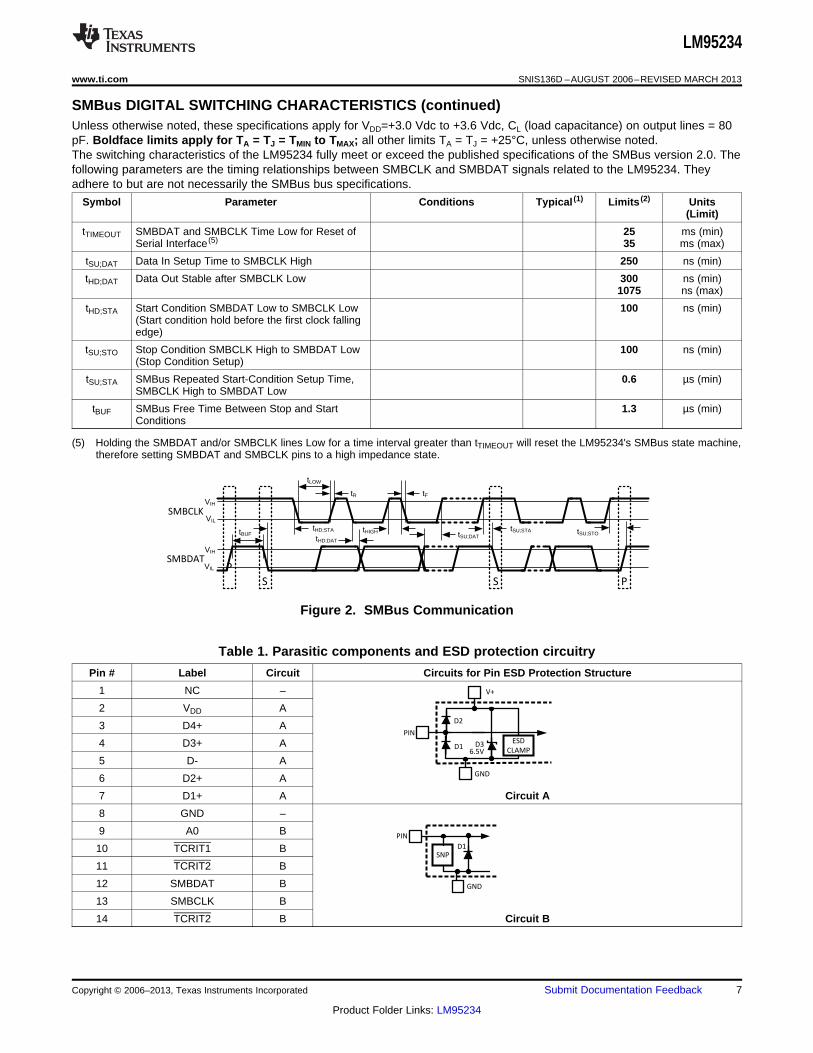
SMBus DIGITAL SWITCHING CHARACTERISTICS (continued)Unless otherwise noted, these specifications apply for VDD=+3.0 Vdc to +3.6 Vdc, CL (load capacitance) on output lines = 80pF. Boldface limits apply for TA = TJ = TMIN to TMAX; all other limits TA = TJ = +25°C, unless otherwise noted.The switching characteristics of the LM95234 fully meet or exceed the published specifications of the SMBus version 2.0. Thefollowing parameters are the timing relationships between SMBCLK and SMBDAT signals related to the LM95234. Theyadhere to but are not necessarily the SMBus bus specifications.
Symbol Parameter Conditions Typical (1) Limits (2) Units(Limit)
tTIMEOUT SMBDAT and SMBCLK Time Low for Reset of 25 ms (min)Serial Interface (5) 35 ms (max)
tSU;DAT Data In Setup Time to SMBCLK High 250 ns (min)
tHD;DAT Data Out Stable after SMBCLK Low 300 ns (min)1075 ns (max)
tHD;STA Start Condition SMBDAT Low to SMBCLK Low 100 ns (min)(Start condition hold before the first clock fallingedge)
tSU;STO Stop Condition SMBCLK High to SMBDAT Low 100 ns (min)(Stop Condition Setup)
tSU;STA SMBus Repeated Start-Condition Setup Time, 0.6 µs (min)SMBCLK High to SMBDAT Low
tBUF SMBus Free Time Between Stop and Start 1.3 µs (min)Conditions
(5) Holding the SMBDAT and/or SMBCLK lines Low for a time interval greater than tTIMEOUT will reset the LM95234's SMBus state machine,therefore setting SMBDAT and SMBCLK pins to a high impedance state.
Figure 2. SMBus Communication
Table 1. Parasitic components and ESD protection circuitry
Pin # Label Circuit Circuits for Pin ESD Protection Structure
1 NC –
2 VDD A
3 D4+ A
4 D3+ A
5 D- A
6 D2+ A
7 D1+ A Circuit A
8 GND –
9 A0 B
10 TCRIT1 B
11 TCRIT2 B
12 SMBDAT B
13 SMBCLK B
14 TCRIT2 B Circuit B
Copyright © 2006–2013, Texas Instruments Incorporated Submit Documentation Feedback 7
Product Folder Links: LM95234

CONVERSION TIME (ms)
100 1000 10000
0.0
0.5
1.0
1.5
2.0
2.5
3.0
AV
ER
AG
E I
DD
(mA
)
VDD = +3.3V
TA = 25°C
LM95234
SNIS136D –AUGUST 2006–REVISED MARCH 2013 www.ti.com
Typical Performance Characteristics
Thermal Diode Capacitor or PCBConversion Rate Effect on Leakage Current Effect on
Average Power Supply Current Remote Diode Temperature Reading
Figure 3. Figure 4.
Remote Temperature Reading Sensitivity to Remote Temperature Reading Sensitivity toThermal Diode Filter Capacitance, Thermal Diode Filter Capacitance,
TruTherm Disabled TruTherm Enabled
Figure 5. Figure 6.
Intel Processor on 65 nm Process or 90 nm ProcessThermal Diode Performance Comparison
Figure 7.
8 Submit Documentation Feedback Copyright © 2006–2013, Texas Instruments Incorporated
Product Folder Links: LM95234
LM95234
www.ti.com SNIS136D –AUGUST 2006–REVISED MARCH 2013
FUNCTIONAL DESCRIPTION
LM95234 is an 11-bit digital temperature sensor with a 2-wire System Management Bus (SMBus) interface thatcan monitor the temperature of four remote diodes as well as its own temperature. The LM95234 can be used tovery accurately monitor the temperature of up to four external devices such as microprocessors, graphicsprocessors or diode-connected 2N3904 transistor. The LM95234 includes TruTherm BJT beta compensationtechnology that allows sensing of Intel processors 90 nm or 65 nm process thermal diodes accurately.
The LM95234 reports temperature in two different formats for +127.875°C/–128°C range and 0°C/255°C range.The LM95234 has a Sigma-Delta ADC (Analog-to-Digital Converter) core which provides the first level of noiseimunity. For improved performance in a noisy environment the LM95234 includes programmable digital filters forRemote Diode 1 and 2 temperature readings. When the digital filters are invoked the resolution for Remote Diode1 and 2 readings increases to 0.03125°C. The LM95234 contains a diode model selection register that includesbits for each channel that select between thermal diodes of Intel processors on 65 nm process or 2N3904s. Formaximum flexibility and best accuracy the LM95234 includes offset registers that allow calibration of other diodetypes.
Diode fault detection circuitry in the LM95234 can detect the absence or fault state of a remote diode: whetherD+ is shorted to VDD, D- or ground, or whether D+ is floating.
The LM95234 TCRIT1, TCRIT2 and TCRIT3 active low outputs are triggered when any unmasked channelexceeds its corresponding programmable limit and can be used to shutdown the system, to turn on the systemfans or as a microcontroller interrupt function. The current status of the TCRIT1, TCRIT2 and TCRIT3 pins canbe read back from the status registers via the SMBus interface. Two of the remote channels have two separatelimits each that control the TCRIT1 and TCRIT2 pins. The remaining two channels and the local channel eachhave one limit to control both the TCRIT1 and TCRIT2 pins. The TCRIT3 pin shares the limits of the TCRIT2 pinbut allows for different masking options. All limits have a shared programmable hysteresis register.
Remote Diode 1 and 2 temperature channels have programmable digital filters while the other two remotetemperature channels utilize a fault-queue in order to avoid false triggering the TCRIT pins.
LM95234 has a three-level address pin to connect up to 3 devices to the same SMBus master. LM95234 alsohas programmable conversion rate register as well as a shutdown mode for power savings. One round ofconversions can be triggered in shutdown mode by writing to the one-shot register through the SMBus interface.LM95234 can be programmed to turn off unused channels for more power savings.
The LM95234 register set has an 8-bit data structure and includes:1. Temperature Value Registers with signed format
– Most-Significant-Byte (MSB) and Least-Significant-Byte (LSB) Local Temperature– MSB and LSB Remote Temperature 1– MSB and LSB Remote Temperature 2– MSB and LSB Remote Temperature 3– MSB and LSB Remote Temperature 4
2. Temperature Value Registers with unsigned format– MSB and LSB Remote Temperature 1– MSB and LSB Remote Temperature 2– MSB and LSB Remote Temperature 3– MSB and LSB Remote Temperature 4
3. Diode Configuration Registers– Diode Model Select– Remote 1 Offset– Remote 2 Offset– Remote 3 Offset– Remote 4 Offset
4. General Configuration Registers– Configuration (Standby, Fault Queue enable for Remote 3 and 4; Conversion Rate)– Channel Conversion Enable
Copyright © 2006–2013, Texas Instruments Incorporated Submit Documentation Feedback 9
Product Folder Links: LM95234
CONVERSION TIME (ms)
100 1000 10000
0.0
0.5
1.0
1.5
2.0
2.5
3.0
AV
ER
AG
E I
DD
(mA
)
VDD = +3.3V
TA = 25°C
LM95234
SNIS136D –AUGUST 2006–REVISED MARCH 2013 www.ti.com
– Filter Setting for Remote 1 and 2– 1-Shot
5. Status Registers– Main Status Register (Busy bit, Not Ready, Status Register 1 to 4 Flags)– Status 1 (diode fault)– Status 2 (TCRIT1)– Status 3 (TCRIT2)– Status 4 (TCRIT3)– Diode Model Status
6. Mask Registers– TCRIT1 Mask– TCRIT2 Mask– TCRIT3 Mask
7. Limit Registers– Local Tcrit Limit– Remote 1 Tcrit-1 Limit– Remote 2 Tcrit-1 Limit– Remote 3 Tcrit Limit– Remote 4 Tcrit Limit– Remote 1 Tcrit-2 and Tcrit-3 Limit– Remote 2 Tcrit-2 and Tcrit-3 Limit– Common Tcrit Hysteresis
8. Manufacturer ID Register9. Revision ID Register
CONVERSION SEQUENCE
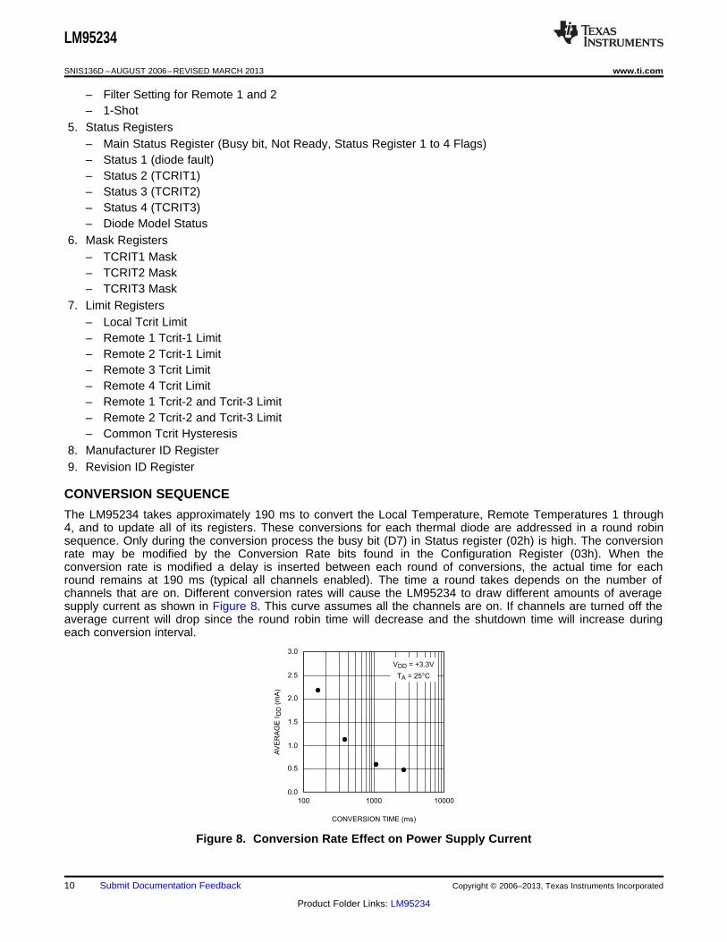
The LM95234 takes approximately 190 ms to convert the Local Temperature, Remote Temperatures 1 through4, and to update all of its registers. These conversions for each thermal diode are addressed in a round robinsequence. Only during the conversion process the busy bit (D7) in Status register (02h) is high. The conversionrate may be modified by the Conversion Rate bits found in the Configuration Register (03h). When theconversion rate is modified a delay is inserted between each round of conversions, the actual time for eachround remains at 190 ms (typical all channels enabled). The time a round takes depends on the number ofchannels that are on. Different conversion rates will cause the LM95234 to draw different amounts of averagesupply current as shown in Figure 8. This curve assumes all the channels are on. If channels are turned off theaverage current will drop since the round robin time will decrease and the shutdown time will increase duringeach conversion interval.
Figure 8. Conversion Rate Effect on Power Supply Current
10 Submit Documentation Feedback Copyright © 2006–2013, Texas Instruments Incorporated
Product Folder Links: LM95234

LM95234
www.ti.com SNIS136D –AUGUST 2006–REVISED MARCH 2013
POWER-ON-DEFAULT STATES
LM95234 always powers up to these known default states. The LM95234 remains in these states until after thefirst conversion.1. All Temperature readings set to 0°C until the end of the first conversion2. Diode Model Select: Remote 1 set to 65 nm Intel processor, Remote 2-4 set to MMBT39043. Remote offset for all channels 0°C4. Configuration: Active converting, Fault Queue enabled for Remote 3 and 45. Continuous conversion with all channels enabled, time = 1s6. Enhanced digital filter enabled for Remote 1 and 27. Status Registers depends on state of thermal diode inputs8. Local and Remote Temperature Limits for TCRIT1, TCRIT2 and TCRIT3 outputs:
Output Pin Temperature Channel Limit
Remote 4 Remote 3 Remote 2 Remote 1 Local(°C) (°C) (°C) (°C) (°C)
TCRIT1 Masked, Masked, 110 110 Masked,85 85 85
TCRIT2 85 85 85 85 85
TCRIT3 85 85 Masked, Masked, Masked,85 85 85
9. Manufacturers ID set to 01h10. Revision ID set to 79h
SMBus INTERFACE
The LM95234 operates as a slave on the SMBus, so the SMBCLK line is an input and the SMBDAT line isbidirectional. The LM95234 never drives the SMBCLK line and it does not support clock stretching. According toSMBus specifications, the LM95234 has a 7-bit slave address. Three SMBus device address can be selected byconnecting A0 (pin 6) to either Low, Mid-Supply or High voltages. The LM95234 has the following SMBus slaveaddress:
A0 Pin State SMBus Device Address A[6:0]
Hex Binary
Low 18h 001 1000
Mid-Supply 4Dh 100 1101
High 4Eh 100 1110
TEMPERATURE CONVERSION SEQUENCE
Each of the 5 temperature channels of LM95234 can be turned OFF independent from each other via theChannel Enable Register. Turning off unused channels will increase the conversion speed in the fastestconversion speed mode. If the slower conversion speed settings are used, disabling unused channels will reducethe average power consumption of LM95234.
DIGITAL FILTER
In order to suppress erroneous remote temperature readings due to noise as well as increase the resolution ofthe temperature, the LM95234 incorporates a digital filter for Remote 1 and 2 Temperature Channels. When afilter is enabled the filtered readings are used for the TCRIT comparisons. There are two possible digital filtersettings that are enabled through the Filter Setting Register at register address 0Fh. The filter for each channelcan be set according to the following table:
Copyright © 2006–2013, Texas Instruments Incorporated Submit Documentation Feedback 11
Product Folder Links: LM95234

0 50 100 150 200
SAMPLE NUMBER
TE
MP
ER
AT
UR
E (
o C)
LM95234 with Filter On
LM95234 withFilter Off
25
27
29
31
33
35
37
39
41
43
45
LM95234
SNIS136D –AUGUST 2006–REVISED MARCH 2013 www.ti.com
R1F[1:0] or R2F[1:0] Filter Setting
0 0 No Filter
0 1 Filter (equivalent to Level 2 filter of the LM86/LM89)
1 0 Reserved
1 1 Enhanced Filter (Filter with transient noise clipping)
Figure 9 through Figure 11 describe the filter output in response to a step input and an impulse input.
Figure 9. Seventeen and fifty degree step response Figure 10. Impulse response with input transientsless than 4°C
Figure 11. Impulse response with input transients Figure 12. Digital Filter Response in a typical Intelgreat than 4°C processor on a 65 nm or 90 nm process. The filter
curves were purposely offset for clarity.
Figure 12 shows the filter in use in a typical Intel processor on a 65/90 nm process system. Note that the twocurves have been purposely offset for clarity. Inserting the filter does not induce an offset as shown.
FAULT QUEUE
In order to suppress erroneous TCRIT1,TCRIT2 and TCRIT3 triggering the LM95234 incorporates a Fault Queuefor the unfiltered remote channels 3 and 4. The Fault Queue acts to ensure the remote temperaturemeasurement of these channels is genuinely beyond the corresponding Tcrit limit by not triggering until threeconsecutive out of limit measurements have been made, see Figure 13 for an example. The Fault Queuedefaults on upon power-up. The fault queue for channels 3 and 4 can be turned ON or OFF via bits 0 and 1 ofthe Configuration Register. When the fault queue is enabled, the TCRIT1, TCRIT2 and TCRIT3 pins will betriggered if the temperature is above the Tcrit limit for 3 consecutive conversions and the corresponding mask bitis 0 in the TCRIT Mask registers. Similarly the temperature needs to be below the Tcrit limit minus the hysteresisvalue for three consecutive conversions for the TCRIT1, TRCIT2 and TCRIT3 pins to deactivate.
12 Submit Documentation Feedback Copyright © 2006–2013, Texas Instruments Incorporated
Product Folder Links: LM95234

Remote 4 Tcrit Limit
Register Value
Status 4 Register R4T3 Bit
Remote 4 Temperature Readings
SAMPLE NUMBER
n n+1
n+2
n+3
n+4
n+5
n+6
n+7
n+8
n+9
n+10
n+11
LM95234
www.ti.com SNIS136D –AUGUST 2006–REVISED MARCH 2013
Figure 13. Fault Queue Response Diagram (with 0°C hysteresis)
TEMPERATURE DATA FORMAT
Temperature data can only be read from the Local and Remote Temperature value registers. The data format forall temperature values is left justified 16-bit word available in two 8-bit registers. Unused bits will always report"0". All temperature data is clamped and will not roll over when a temperature exceeds full-scale value.
Remote temperature data for all channels can be represented by an 11-bit, two's complement word or unsignedbinary word with an LSb (Least Significant Bit) equal to 0.125°C.
Table 2. 11-bit, 2's Complement (10-bit plus sign)
Temperature Digital Output
Binary Hex
+125°C 0111 1101 0000 0000 7D00h
+25°C 0001 1001 0000 0000 1900h
+1°C 0000 0001 0000 0000 0100h
+0.125°C 0000 0000 0010 0000 0020h
0°C 0000 0000 0000 0000 0000h
−0.125°C 1111 1111 1110 0000 FFE0h
−1°C 1111 1111 0000 0000 FF00h
−25°C 1110 0111 0000 0000 E700h
−55°C 1100 1001 0000 0000 C900h
Table 3. 11-bit, Unsigned Binary
Temperature Digital Output
Binary Hex
+255.875°C 1111 1111 1110 0000 FFE0h
+255°C 1111 1111 0000 0000 FF00h
+201°C 1100 1001 0000 0000 C900h
+125°C 0111 1101 0000 0000 7D00h
+25°C 0001 1001 0000 0000 1900h
+1°C 0000 0001 0000 0000 0100h
+0.125°C 0000 0000 0010 0000 0020h
0°C 0000 0000 0000 0000 0000h
Copyright © 2006–2013, Texas Instruments Incorporated Submit Documentation Feedback 13
Product Folder Links: LM95234
LM95234
SNIS136D –AUGUST 2006–REVISED MARCH 2013 www.ti.com
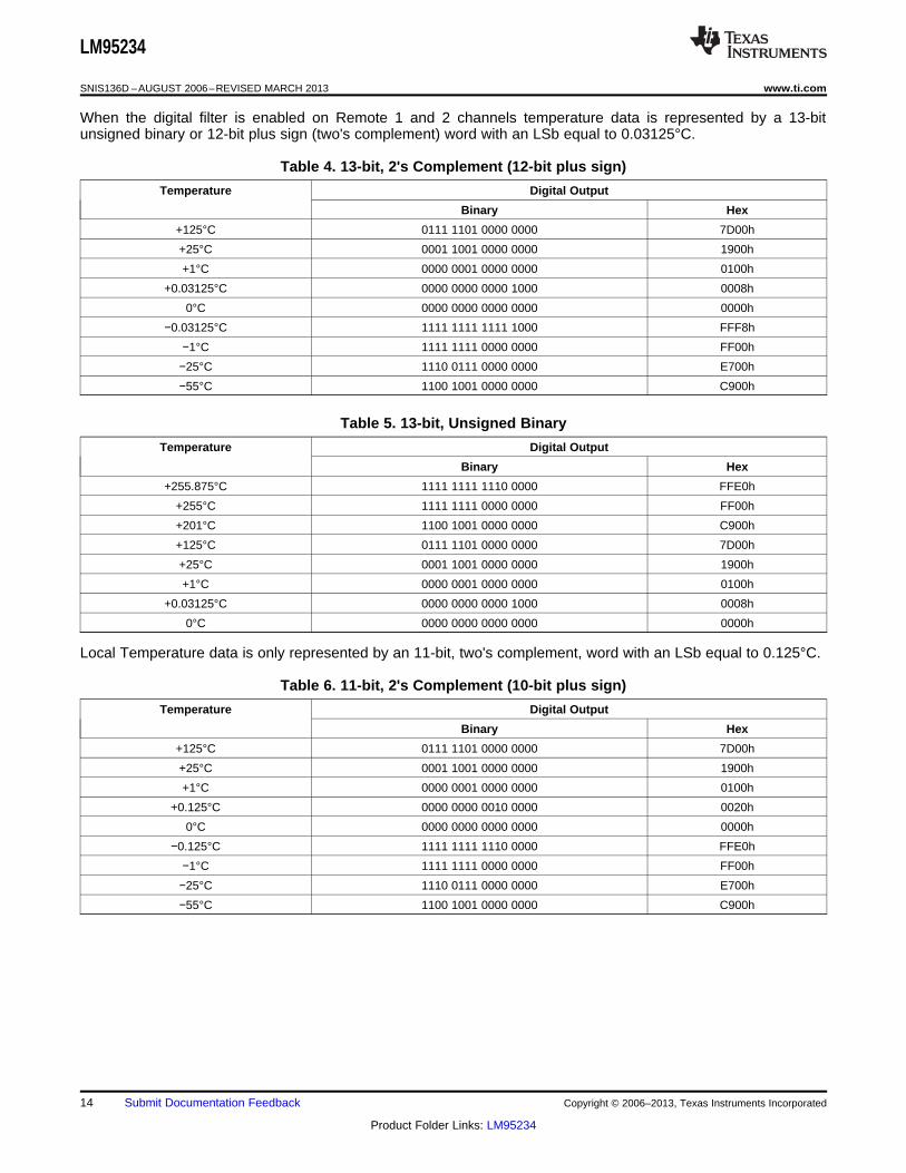
When the digital filter is enabled on Remote 1 and 2 channels temperature data is represented by a 13-bitunsigned binary or 12-bit plus sign (two's complement) word with an LSb equal to 0.03125°C.
Table 4. 13-bit, 2's Complement (12-bit plus sign)
Temperature Digital Output
Binary Hex
+125°C 0111 1101 0000 0000 7D00h
+25°C 0001 1001 0000 0000 1900h
+1°C 0000 0001 0000 0000 0100h
+0.03125°C 0000 0000 0000 1000 0008h
0°C 0000 0000 0000 0000 0000h
−0.03125°C 1111 1111 1111 1000 FFF8h
−1°C 1111 1111 0000 0000 FF00h
−25°C 1110 0111 0000 0000 E700h
−55°C 1100 1001 0000 0000 C900h
Table 5. 13-bit, Unsigned Binary
Temperature Digital Output
Binary Hex
+255.875°C 1111 1111 1110 0000 FFE0h
+255°C 1111 1111 0000 0000 FF00h
+201°C 1100 1001 0000 0000 C900h
+125°C 0111 1101 0000 0000 7D00h
+25°C 0001 1001 0000 0000 1900h
+1°C 0000 0001 0000 0000 0100h
+0.03125°C 0000 0000 0000 1000 0008h
0°C 0000 0000 0000 0000 0000h
Local Temperature data is only represented by an 11-bit, two's complement, word with an LSb equal to 0.125°C.
Table 6. 11-bit, 2's Complement (10-bit plus sign)
Temperature Digital Output
Binary Hex
+125°C 0111 1101 0000 0000 7D00h
+25°C 0001 1001 0000 0000 1900h
+1°C 0000 0001 0000 0000 0100h
+0.125°C 0000 0000 0010 0000 0020h
0°C 0000 0000 0000 0000 0000h
−0.125°C 1111 1111 1110 0000 FFE0h
−1°C 1111 1111 0000 0000 FF00h
−25°C 1110 0111 0000 0000 E700h
−55°C 1100 1001 0000 0000 C900h
14 Submit Documentation Feedback Copyright © 2006–2013, Texas Instruments Incorporated
Product Folder Links: LM95234
LM95234
www.ti.com SNIS136D –AUGUST 2006–REVISED MARCH 2013
SMBDAT OPEN-DRAIN OUTPUT
The SMBDAT output is an open-drain output and does not have internal pull-ups. A “high” level will not beobserved on this pin until pull-up current is provided by some external source, typically a pull-up resistor. Choiceof resistor value depends on many system factors but, in general, the pull-up resistor should be as large aspossible without effecting the SMBus desired data rate. This will minimize any internal temperature readingerrors due to internal heating of the LM95234. The maximum resistance of the pull-up to provide a 2.1V highlevel, based on LM95234 specification for High Level Output Current with the supply voltage at 3.0V, is 82 kΩ(5%) or 88.7 kΩ (1%).
TCRIT1, TCRIT2, and TCRIT3 OUTPUTS
The LM95234's TCRIT pins are active-low open-drain outputs and do not include internal pull-up resistors. A“high” level will not be observed on these pins until pull-up current is provided by some external source, typicallya pull-up resistor. Choice of resistor value depends on many system factors but, in general, the pull-up resistorshould be as large as possible without effecting the performance of the device receiving the signal. This willminimize any internal temperature reading errors due to internal heating of the LM95234. The maximumresistance of the pull-up to provide a 2.1V high level, based on LM95234 specification for High Level OutputCurrent with the supply voltage at 3.0V, is 82 kΩ (5%) or 88.7 kΩ (1%). The three TCRIT pins can each sink 6mA of current and still ensure a "Logic Low" output voltage of 0.4V. If all three pins are set at maximum currentthis will cause a power dissipation of 7.2 mW. This power dissipation combined with a thermal resistance of77.8°C/W will cause the LM95234's junction temperature to rise approximately 0.6°C and thus cause the Localtemperature reading to shift. This can only be cancelled out if the environment that the LM95234 is enclosed inhas stable and controlled air flow over the LM95234, as airflow can cause the thermal resistance to changedramatically.
Tcrit LIMITS AND TCRIT OUTPUTS
Figure 14 describes a simplified diagram of the temperature comparison and status register logic. Logic diagramsfor the TCRIT1, TCRIT2, and TCRIT3 outputs describes a simplified logic diagram of the circuitry associated withthe status registers, mask registers and the TCRIT output pins.
Copyright © 2006–2013, Texas Instruments Incorporated Submit Documentation Feedback 15
Product Folder Links: LM95234

Status 2 (TCRIT1)
R4T1
R3T1
R2T1
R1T1
LT1
Common Tcrit Hysteresis
Remote Temp 4
Remote 4 Tcrit Limit
+-
ABA
B
AtBA
BQS
R
Remote Temp 3
Remote 3 Tcrit Limit
+-
ABA
B
AtBA
BQS
R
Remote Temp 2
Remote 2 Tcrit-1 Limit
+-
ABA
B
AtBA
BQS
R
Remote 1 Tcrit2 & Tcrit-3 Limit
+-
ABA
B
AtBA
BQS
R
Local Temp
Local Tcrit Limit
+-
ABA
B
AtBA
BQS
R
Status 4 (TCRIT3)
R4T3
R3T3
R2T3
R1T3
LT3
Status 3 (TCRIT2)
R4T2
R3T2
R2T2
R1T2
LT2
Remote 2 Tcrit-2 & Tcrit-3 Limit
+-
ABA
B
AtBA
BQS
R
Remote Temp 1
Remote 1 Tcrit-1 Limit
+-
ABA
B
AtBA
BQS
R
LM95234
SNIS136D –AUGUST 2006–REVISED MARCH 2013 www.ti.com
Figure 14. Temperature Comparison Logic and Status Register Simplified Diagram
16 Submit Documentation Feedback Copyright © 2006–2013, Texas Instruments Incorporated
Product Folder Links: LM95234

TCRIT3
Status 4
(TCRIT3)
R4T3
R3T3
R2T3
R1T3
LT3
TCRIT3
Mask
R4TM
R3TM
R2T2M
R1T2M
LTM
Status 1 (Diode
Fault)
R4DO
R4DS
R3DO
R3DS
R2DO
R2DS
R1DO
R1DS
TCRIT1
Status 1
(Diode Fault)
R4DO
R4DS
R3DO
R3DS
R2DO
R2DS
R1DO
R1DS
Status 2
(TCRIT1)
R4T1
R3T1
R2T1
R1T1
LT1
TCRIT1
Mask
R4TM
R3TM
R2T1M
R1T1M
LTM
TCRIT2
Status 3
(TCRIT2)
R4T2
R3T2
R2T2
R1T2
LT2
TCRIT2
Mask
R4TM
R3TM
R2T2M
R1T2M
LTM
Status 1
(Diode Fault)
R4DO
R4DS
R3DO
R3DS
R2DO
R2DS
R1DO
R1DS
LM95234
www.ti.com SNIS136D –AUGUST 2006–REVISED MARCH 2013
Logic diagrams for the TCRIT1, TCRIT2, and TCRIT3 outputs
Figure 15. TCRIT1 Mask Register, Status Register 1 Figure 16. TCRIT2 Mask Register, Status Register 1and 2, and TCRIT1 output logic diagram. and 3, and TCRIT2 output logic diagram.
Figure 17. TCRIT3 Mask Register, Status Register 1 and 4, and TCRIT3 output logic diagram.
Copyright © 2006–2013, Texas Instruments Incorporated Submit Documentation Feedback 17
Product Folder Links: LM95234

T_CRITnOutput Pin
Local Tcrit Limit
LocalTemperature
Status bit LTn
Local Tcrit Limit - Common Hysteresis
Common Hysteresis
LM95234
SNIS136D –AUGUST 2006–REVISED MARCH 2013 www.ti.com
If enabled, local temperature is compared to the user programmable Local Tcrit Limit Register (Default Value =85°C). The result of this comparison is stored in Status Register 2, Status Register 3 and Status Register 4 (seeLogic diagrams for the TCRIT1, TCRIT2, and TCRIT3 outputs).The comparison result can trigger TCRIT1 pin,TCRIT2 pin or TCRIT3 pin depending on the settings in the TCRIT1 Mask, TCRIT2 Mask and TRCIT3 MaskRegisters (see Logic diagrams for the TCRIT1, TCRIT2, and TCRIT3 outputs). The comparison result can alsobe read back from the Status Register 2, Status Register 3 and Status Register 4.
If enabled, remote temperature 1 is compared to the user programmable Remote 1 Tcrit-1 Limit Register (DefaultValue 110°C) and Remote 1 Tcrit-2 Limit Register (Default Value = 85°C). The result of this comparison is storedin Status Register 2, Status Register 3 and Status Register 4 (see Figure 14). The comparison result can triggerTCRIT1 pin, TCRIT2 pin or TCRIT3 pin depending on the settings in the TCRIT1 Mask, TCRIT2 Mask andTRCIT3 Mask Registers (see Logic diagrams for the TCRIT1, TCRIT2, and TCRIT3 outputs). The comparisonresult can also be read back from the Status Register 2, Status Register 3 and Status Register 4. The remotetemperature 2 operates in a similar manner to remote temperature 1 using its associated user programmablelimit registers: Remote 2 Tcrit-1 Limit Register (Default Value 110°C) and Remote 2 Tcrit-2 Limit Register(Default Value = 85°C). When enabled, the remote temperature 3 is compared to the user programmableRemote 3 Tcrit Limit Register (Default Value 85°C). The comparison result can trigger TCRIT1 pin, TCRIT2 pinor TCRIT3 pin depending on the settings in the TCRIT1 Mask, TCRIT2 Mask and TCRIT3 Mask Registers. Thecomparison result can also be read back from the Status Register 2, Status Register 3 and Status Register 4.The remote temperature 4 operates in a similar manner to remote temperature 3 using its associated userprogrammable limit register: Remote 4 Tcrit Limit Register (Default Value 85°C).
Table 7. Limit assignments for each TCRIT output pin:
TCRIT1 TCRIT2 TCRIT3
Remote 4 Remote 4 Remote 4 Remote 4Tcrit Limit Tcrit Limit Tcrit Limit
Remote 3 Remote 3 Remote 3 Remote 3Tcrit Limit Tcrit Limit Tcrit Limit
Remote 2 Remote 2 Remote 2 Remote 2Tcrit-1 Limit Tcrit-2 Limit Tcrit-2 Limit
Remote 1 Remote 1 Remote 1 Remote 1Tcrit-1 Limit Tcrit-2 Limit Tcrit-2 Limit
Local Local Local LocalTcrit Limit Tcrit Limit Tcrit Limit
Figure 18. TCRIT response diagram (masking options not included)
The TCRIT response diagram of Figure 18 shows the local temperature interaction with the Tcrit limit andhysteresis value. As can be seen in the diagram when the local temperature exceeds the Tcrit limit register valuethe LTn Status bit is set and the T_CRITn output(s) is/are activated. The Status bit(s) and outputs are notdeactivated until the temperature goes below the value calculated by subtracting the Common Hysteresis valueprogrammed from the limit. This diagram mainly shows an example function of the hysteresis and is not meant toshow complete function of the possible settings and options of all the TCRIT outputs and limit values.
18 Submit Documentation Feedback Copyright © 2006–2013, Texas Instruments Incorporated
Product Folder Links: LM95234

D7 D6 D5 D4 D3 D2 D1 D0
1 9 1 9
Ackby
LM95234
Start byMaster
R/W
Frame 1Serial Bus Address Byte
Frame 2Command Byte
Ackby
LM95234
D7 D6 D5 D4 D3 D2 D1 D0
1 9
Frame 3Data Byte
Ack by LM95234
Stopby
Master
SMBCLK
SMBDAT
SMBCLK (Continued)
SMBDAT (Continued)
A5 A3 A2 A0A6 A4 A1
LM95234
www.ti.com SNIS136D –AUGUST 2006–REVISED MARCH 2013
DIODE FAULT DETECTION
The LM95234 is equipped with operational circuitry designed to detect fault conditions concerning the remotediodes. In the event that the D+ pin is detected as shorted to GND, D−, VDD or D+ is floating, the RemoteTemperature reading is –128.000 °C if signed format is selected and 0 °C if unsigned format is selected. Inaddition, the appropriate status register bits RD1M or RD2M (D1 or D0) are set.
COMMUNICATING with the LM95234
The data registers in the LM95234 are selected by the Command Register. At power-up the Command Registeris set to “00”, the location for the Read Local Temperature Register. The Command Register latches the lastlocation it was set to. Each data register in the LM95234 falls into one of three types of user accessibility:1. Read only2. Write only3. Write/Read same address
A Write to the LM95234 will always include the address byte and the command byte. A write to any registerrequires one data byte.
Reading the LM95234 can take place either of two ways:1. If the location latched in the Command Register is correct (most of the time it is expected that the Command
Register will point to one of the Read Temperature Registers because that will be the data most frequentlyread from the LM95234), then the read can simply consist of an address byte, followed by retrieving the databyte.
2. If the Command Register needs to be set, then an address byte, command byte, repeat start, and anotheraddress byte will accomplish a read.
The data byte has the most significant bit first. At the end of a read, the LM95234 can accept either acknowledgeor No Acknowledge from the Master (No Acknowledge is typically used as a signal for the slave that the Masterhas read its last byte). It takes the LM95234 190 ms (typical, all channels enabled) to measure the temperatureof the remote diodes and internal diode. When retrieving all 11 bits from a previous remote diode temperaturemeasurement, the master must insure that all 11 bits are from the same temperature conversion. This may beachieved by reading the MSB register first. The LSB will be locked after the MSB is read. The LSB will beunlocked after being read. If the user reads MSBs consecutively, each time the MSB is read, the LSB associatedwith that temperature will be locked in and override the previous LSB value locked-in.
SMBus Timing Diagrams
Figure 19. Serial Bus Write to the internal Command Register followed by a the Data Byte
Copyright © 2006–2013, Texas Instruments Incorporated Submit Documentation Feedback 19
Product Folder Links: LM95234

D7 D6 D5 D4 D3 D2 D1 D0
1 9 1 9
Ackby
LM95234
Start byMaster
RepeatStart byMaster
R/W
Frame 1Serial Bus Address Byte
Frame 2Command Byte
Ackby
LM95234
D7 D6 D5 D4 D3 D2 D1 D0
1 9 1 9
Ackby
LM95234
R/W
Frame 3Serial Bus Address Byte
Frame 4Data Byte from the LM95234
No Ackby
Master
Stopby
Master
SMBCLK
SMBDAT
SMBCLK (Continued)
SMBDAT (Continued)
A5 A3 A2 A0A6 A4 A1
A5 A3 A2 A0A6 A4 A1
D7 D6 D5 D4 D3 D2 D1 D0
1 9 1 9
Ackby
LM95234
Start byMaster
R/W
Frame 1Serial Bus Address Byte
Frame 2Data Byte from the LM95234
NoAckby
Master
SMBCLK
SMBDAT
Stopby
Master
A5 A3 A2 A0A6 A4 A1
D7 D6 D5 D4 D3 D2 D1 D0
1 9 1 9
Ackby
LM95234
Start byMaster
R/W
Frame 1Serial Bus Address Byte
Frame 2Command Byte
Ack byLM95234
SMBCLK
SMBDAT A5 A3 A2 A0A6 A4 A1
Stopby
Master
LM95234
SNIS136D –AUGUST 2006–REVISED MARCH 2013 www.ti.com
Figure 20. Serial Bus Write to the Internal Command Register
Figure 21. Serial Bus Read from a Register with the Internal Command Register preset to desired value.
Figure 22. Serial Bus Write followed by a Repeat Start and Immediate Read
SERIAL INTERFACE RESET
In the event that the SMBus Master is RESET while the LM95234 is transmitting on the SMBDAT line, theLM95234 must be returned to a known state in the communication protocol. This may be done in one of twoways:1. When SMBDAT is LOW, the LM95234 SMBus state machine resets to the SMBus idle state if either
SMBDAT or SMBCLK are held low for more than 35ms (tTIMEOUT). Note that according to SMBusspecification 2.0 all devices are to timeout when either the SMBCLK or SMBDAT lines are held low for 25-35ms. Therefore, to insure a timeout of all devices on the bus the SMBCLK or SMBDAT lines must be heldlow for at least 35ms.
2. When SMBDAT is HIGH, have the master initiate an SMBus start. The LM95234 will respond properly to anSMBus start condition at any point during the communication. After the start the LM95234 will expect anSMBus Address address byte.
20 Submit Documentation Feedback Copyright © 2006–2013, Texas Instruments Incorporated
Product Folder Links: LM95234
LM95234
www.ti.com SNIS136D –AUGUST 2006–REVISED MARCH 2013
ONE-SHOT CONVERSION
The One-Shot register is used to initiate a round of conversions and comparisons when the device is in standbymode, after which the device returns to standby. This is not a data register and it is the write operation thatcauses the one-shot conversion. The data written to this address is irrelevant and is not stored. A zero willalways be read from this register. All the channels that are enabled in the Channel Enable Register will beconverted once and the TCRIT1, TCRIT2 and TCRIT3 pins will reflect the comparison results based on thisround of conversion results of the channels that are not masked.
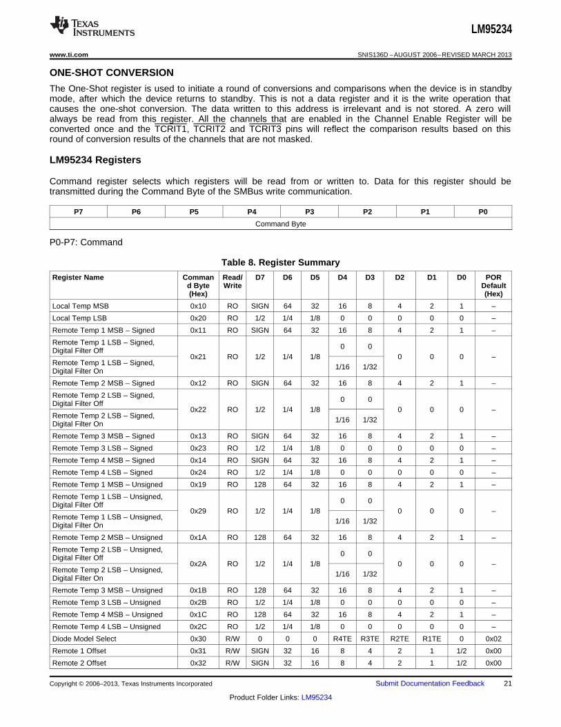
LM95234 Registers
Command register selects which registers will be read from or written to. Data for this register should betransmitted during the Command Byte of the SMBus write communication.
P7 P6 P5 P4 P3 P2 P1 P0
Command Byte
P0-P7: Command
Table 8. Register Summary
Register Name Comman Read/ D7 D6 D5 D4 D3 D2 D1 D0 PORd Byte Write Default(Hex) (Hex)
Local Temp MSB 0x10 RO SIGN 64 32 16 8 4 2 1 –
Local Temp LSB 0x20 RO 1/2 1/4 1/8 0 0 0 0 0 –
Remote Temp 1 MSB – Signed 0x11 RO SIGN 64 32 16 8 4 2 1 –
Remote Temp 1 LSB – Signed, 0 0Digital Filter Off0x21 RO 1/2 1/4 1/8 0 0 0 –
Remote Temp 1 LSB – Signed, 1/16 1/32Digital Filter On
Remote Temp 2 MSB – Signed 0x12 RO SIGN 64 32 16 8 4 2 1 –
Remote Temp 2 LSB – Signed, 0 0Digital Filter Off0x22 RO 1/2 1/4 1/8 0 0 0 –
Remote Temp 2 LSB – Signed, 1/16 1/32Digital Filter On
Remote Temp 3 MSB – Signed 0x13 RO SIGN 64 32 16 8 4 2 1 –
Remote Temp 3 LSB – Signed 0x23 RO 1/2 1/4 1/8 0 0 0 0 0 –
Remote Temp 4 MSB – Signed 0x14 RO SIGN 64 32 16 8 4 2 1 –
Remote Temp 4 LSB – Signed 0x24 RO 1/2 1/4 1/8 0 0 0 0 0 –
Remote Temp 1 MSB – Unsigned 0x19 RO 128 64 32 16 8 4 2 1 –
Remote Temp 1 LSB – Unsigned, 0 0Digital Filter Off0x29 RO 1/2 1/4 1/8 0 0 0 –
Remote Temp 1 LSB – Unsigned, 1/16 1/32Digital Filter On
Remote Temp 2 MSB – Unsigned 0x1A RO 128 64 32 16 8 4 2 1 –
Remote Temp 2 LSB – Unsigned, 0 0Digital Filter Off0x2A RO 1/2 1/4 1/8 0 0 0 –
Remote Temp 2 LSB – Unsigned, 1/16 1/32Digital Filter On
Remote Temp 3 MSB – Unsigned 0x1B RO 128 64 32 16 8 4 2 1 –
Remote Temp 3 LSB – Unsigned 0x2B RO 1/2 1/4 1/8 0 0 0 0 0 –
Remote Temp 4 MSB – Unsigned 0x1C RO 128 64 32 16 8 4 2 1 –
Remote Temp 4 LSB – Unsigned 0x2C RO 1/2 1/4 1/8 0 0 0 0 0 –
Diode Model Select 0x30 R/W 0 0 0 R4TE R3TE R2TE R1TE 0 0x02
Remote 1 Offset 0x31 R/W SIGN 32 16 8 4 2 1 1/2 0x00
Remote 2 Offset 0x32 R/W SIGN 32 16 8 4 2 1 1/2 0x00
Copyright © 2006–2013, Texas Instruments Incorporated Submit Documentation Feedback 21
Product Folder Links: LM95234

LM95234
SNIS136D –AUGUST 2006–REVISED MARCH 2013 www.ti.com
Table 8. Register Summary (continued)
Register Name Comman Read/ D7 D6 D5 D4 D3 D2 D1 D0 PORd Byte Write Default(Hex) (Hex)
Remote 3 Offset 0x33 R/W SIGN 32 16 8 4 2 1 1/2 0x00
Remote 4 Offset 0x34 R/W SIGN 32 16 8 4 2 1 1/2 0x00
Configuration 0x03 R/W – STBY – – – – R4QE R3QE 0x03
Conversion Rate 0x04 R/W – – – – – – CR1 CR0 0x02
Channel Conversion Enable 0x05 R/W – – – R4CE R3CE R2CE R1CE LCE 0x1F
Filter Setting 0x06 R/W – – – – R2F1 R2F0 R1F1 R1F0 0x0F
1-shot 0x0F WO – – – – – – – – –
Common Status Register 0x02 RO BUSY NR – – SR4F SR3F SR2F SR1F 0x00
Status 1 (Diode Fault) 0x07 RO R4DO R4DS R3DO R3DS R2DO R2DS R1DO R1DS –
Status 2 (TCRIT1) 0x08 RO – – – R4T1 R3T1 R2T1 R1T1 LT1 –
Status 3 (TCRIT2) 0x09 RO – – – R4T2 R3T2 R2T2 R1T2 LT2 –
Status 4 (TCRIT3) 0x0A RO – – – R4T3 R3T3 R2T3 R1T3 LT3 –
Diode Model Status (TruTherm on 0x38 RO – – – R4TD R3TD R2TD R1TD – –and 3904 connected)
TCRIT1 Mask 0x0C R/W – – – R4TM R3TM R2T1M R1T1M LTM 0x19
TCRIT2 Mask 0x0D R/W – – – R4TM R3TM R2T2M R1T2M LTM 0x00
TCRIT3 Mask 0x0E R/W – – – R4TM R3TM R2T2M R1T2M LTM 0x07
Local Tcrit Limit 0x40 R/W 0 64 32 16 8 4 2 1 0x55
Remote 1 Tcrit-1 Limit 0x41 R/W 128 64 32 16 8 4 2 1 0x6E
Remote 2 Tcrit-1 Limit 0x42 R/W 128 64 32 16 8 4 2 1 0x6E
Remote 3 Tcrit Limit 0x43 R/W 128 64 32 16 8 4 2 1 0x55
Remote 4 Tcrit Limit 0x44 R/W 128 64 32 16 8 4 2 1 0x55
Remote 1 Tcrit-2 and Tcrit-3 Limit 0x49 R/W 128 64 32 16 8 4 2 1 0x55
Remote 2 Tcrit-2 and Tcrit-3 Limit 0x4A R/W 128 64 32 16 8 4 2 1 0x55
Common Tcrit Hysteresis 0x5A R/W 0 0 0 16 8 4 2 1 0x0A
Manufacturer ID 0xFE RO 0 0 0 0 0 0 0 1 0x01
Revision ID 0xFF RO 0 1 1 1 1 0 0 1 0x79
VALUE REGISTERS
For data synchronization purposes, the MSB register should be read first if the user wants to read both MSB andLSB registers. The LSB will be locked after the MSB is read. The LSB will be unlocked after being read. If theuser reads MSBs consecutively, each time the MSB is read, the LSB associated with that temperature will belocked in and override the previous LSB value locked-in
Local Value Registers
Register Name Command Read/ D7 D6 D5 D4 D3 D2 D1 D0 PORByte Write Default(Hex) (Hex)
Local Temp MSB 0x10 RO SIGN 64 32 16 8 4 2 1 –
Local Temp LSB 0x20 RO 1/2 1/4 1/8 0 0 0 0 0 –
22 Submit Documentation Feedback Copyright © 2006–2013, Texas Instruments Incorporated
Product Folder Links: LM95234
LM95234
www.ti.com SNIS136D –AUGUST 2006–REVISED MARCH 2013
Bit(s) Bit Name Read/ DescriptionWrite
7 SIGN RO Sign bit The Local temperature MSB value registerrange is +127°C to −128°C. The value6 64 RO bit weight 64°Cprogrammed in this register is used to
5 32 RO bit weight 32°C determine a local temperature error event.
4 16 RO bit weight 16°C
3 8 RO bit weight 8°C
2 4 RO bit weight 4°C
1 2 RO bit weight 2°C
0 1 RO bit weight 1°C
Bit(s) Bit Name Read/ DescriptionWrite
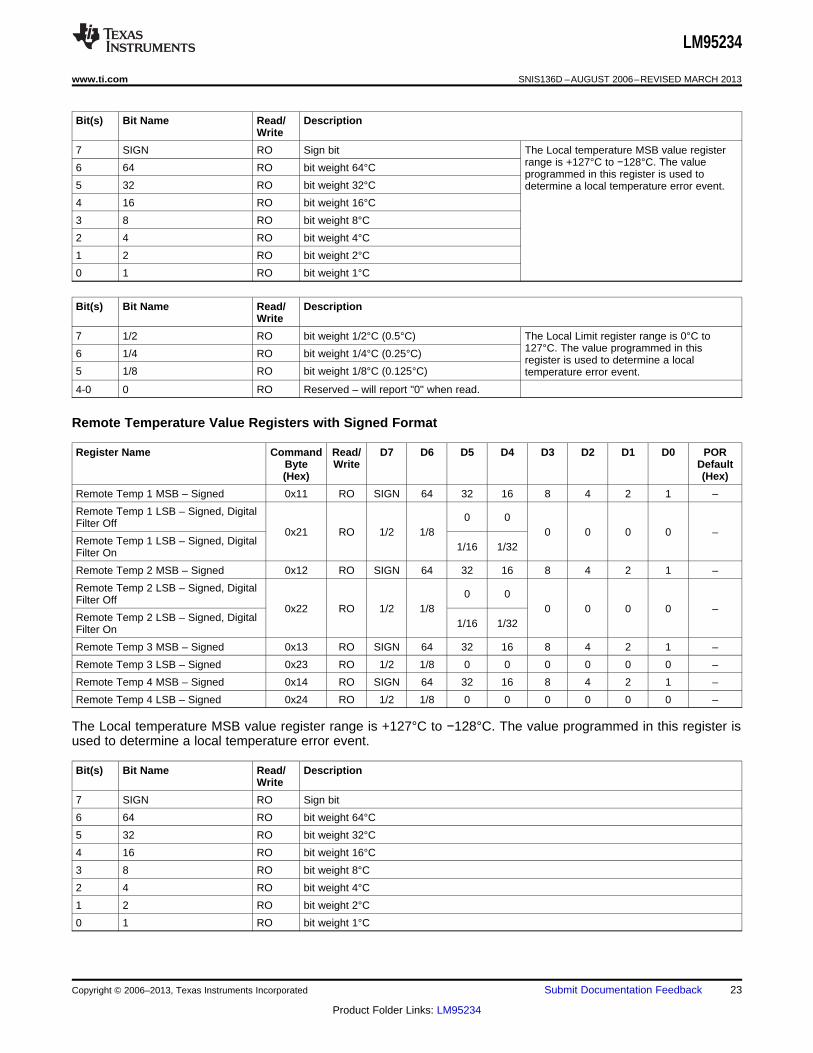
7 1/2 RO bit weight 1/2°C (0.5°C) The Local Limit register range is 0°C to127°C. The value programmed in this6 1/4 RO bit weight 1/4°C (0.25°C)register is used to determine a local
5 1/8 RO bit weight 1/8°C (0.125°C) temperature error event.
4-0 0 RO Reserved – will report "0" when read.
Remote Temperature Value Registers with Signed Format
Register Name Command Read/ D7 D6 D5 D4 D3 D2 D1 D0 PORByte Write Default(Hex) (Hex)
Remote Temp 1 MSB – Signed 0x11 RO SIGN 64 32 16 8 4 2 1 –
Remote Temp 1 LSB – Signed, Digital 0 0Filter Off0x21 RO 1/2 1/8 0 0 0 0 –
Remote Temp 1 LSB – Signed, Digital 1/16 1/32Filter On
Remote Temp 2 MSB – Signed 0x12 RO SIGN 64 32 16 8 4 2 1 –
Remote Temp 2 LSB – Signed, Digital 0 0Filter Off0x22 RO 1/2 1/8 0 0 0 0 –
Remote Temp 2 LSB – Signed, Digital 1/16 1/32Filter On
Remote Temp 3 MSB – Signed 0x13 RO SIGN 64 32 16 8 4 2 1 –
Remote Temp 3 LSB – Signed 0x23 RO 1/2 1/8 0 0 0 0 0 0 –
Remote Temp 4 MSB – Signed 0x14 RO SIGN 64 32 16 8 4 2 1 –
Remote Temp 4 LSB – Signed 0x24 RO 1/2 1/8 0 0 0 0 0 0 –
The Local temperature MSB value register range is +127°C to −128°C. The value programmed in this register isused to determine a local temperature error event.
Bit(s) Bit Name Read/ DescriptionWrite
7 SIGN RO Sign bit
6 64 RO bit weight 64°C
5 32 RO bit weight 32°C
4 16 RO bit weight 16°C
3 8 RO bit weight 8°C
2 4 RO bit weight 4°C
1 2 RO bit weight 2°C
0 1 RO bit weight 1°C
Copyright © 2006–2013, Texas Instruments Incorporated Submit Documentation Feedback 23
Product Folder Links: LM95234

LM95234
SNIS136D –AUGUST 2006–REVISED MARCH 2013 www.ti.com
Bit(s) Bit Name Read/ DescriptionWrite
7 1/2 RO bit weight 1/2°C (0.5°C)
6 1/4 RO bit weight 1/4°C (0.25°C)
5 1/8 RO bit weight 1/8°C (0.125°C)
4 0 or 1/16 RO When the digital filter is disabled this bit will always read "0".When the digital filter is enabled this bit will report 1/16°C (0.0625°C) bit state.
3 0 or 1/32 RO When the digital filter is disabled this bit will always read "0".When the digital filter is enabled this bit will report 1/32°C (0.03125°C) bit state.
2-0 0 RO Reserved – will report "0" when read.
Remote Temperature Value Registers with Unsigned Format
Register Name Command Read/ D7 D6 D5 D4 D3 D2 D1 D0 PORByte Write Default(Hex) (Hex)
Remote Temp 1 MSB – Unsigned 0x19 RO 128 64 32 16 8 4 2 1 –
Remote Temp 1 LSB – Unsigned, 0 0Digital Filter Off0x29 RO 1/2 1/8 0 0 0 0 –
Remote Temp 1 LSB – Unsigned, 1/16 1/32Digital Filter On
Remote Temp 2 MSB – Unsigned 0x1A RO 128 64 32 16 8 4 2 1 –
Remote Temp 2 LSB – Unsigned, 0 0Digital Filter Off0x2A RO 1/2 1/8 0 0 0 0 –
Remote Temp 2 LSB – Unsigned, 1/16 1/32Digital Filter On
Remote Temp 3 MSB – Unsigned 0x1B RO 128 64 32 16 8 4 2 1 –
Remote Temp 3 LSB – Unsigned 0x2B RO 1/2 1/8 0 0 0 0 0 0 –
Remote Temp 4 MSB – Unsigned 0x1C RO 128 64 32 16 8 4 2 1 –
Remote Temp 4 LSB – Unsigned 0x2C RO 1/2 1/8 0 0 0 0 0 0 –
Bit(s) Bit Name Read/ DescriptionWrite
7 SIGN RO bit weight 128°C
6 64 RO bit weight 64°C
5 32 RO bit weight 32°C
4 16 RO bit weight 16°C
3 8 RO bit weight 8°C
2 4 RO bit weight 4°C
1 2 RO bit weight 2°C
0 1 RO bit weight 1°C
Bit(s) Bit Name Read/ DescriptionWrite
7 1/2 RO bit weight 1/2°C (0.5°C)
6 1/4 RO bit weight 1/4°C (0.25°C)
5 1/8 RO bit weight 1/8°C (0.125°C)
4 0 or 1/16 RO When the digital filter is disabled this bit will always read "0".When the digital filter is enabled this bit will report 1/16°C (0.0625°C) bit state.
3 0 or 1/32 RO When the digital filter is disabled this bit will always read "0".When the digital filter is enabled this bit will report 1/32°C (0.03125°C) bit state.
2-0 0 RO Reserved – will report "0" when read.
24 Submit Documentation Feedback Copyright © 2006–2013, Texas Instruments Incorporated
Product Folder Links: LM95234

LM95234
www.ti.com SNIS136D –AUGUST 2006–REVISED MARCH 2013
DIODE CONFIGURATION REGISTERS
Diode Model Select
Register Name Command Read/ D7 D6 D5 D4 D3 D2 D1 D0 PORByte Write Default(Hex) (Hex)
Diode Model Select 0x30 R/W 0 0 0 R4TE R3TE R2TE R1TE 0 0x02
Bit(s) Bit Name Read/ DescriptionWrite
7-5 0 RO Reserved – will report "0" when read.
4 R4TE R/W Remote 4 TruTherm Enable Logic 1 selects diode model 1 TruThermBJT beta compensation technology enabled3 R3TE R/W Remote 3 TruTherm Enable(Ex: Intel 65 nm technology)
2 R2TE R/W Remote 2 TruTherm Enable Logic 0 selects diode model 2 MMBT3904
1 R1TE R/W Remote 1 TruTherm Enable
0 0 RO Reserved – will report "0" when read.
Remote 1-4 Offset
Register Name Command Read/ D7 D6 D5 D4 D3 D2 D1 D0 PORByte Write Default(Hex) (Hex)
Remote 1 Offset 0x31 R/W SIGN 32 16 8 4 2 1 1/2 0x00
Remote 2 Offset 0x32 R/W SIGN 32 16 8 4 2 1 1/2 0x00
Remote 3 Offset 0x33 R/W SIGN 32 16 8 4 2 1 1/2 0x00
Remote 4 Offset 0x34 R/W SIGN 32 16 8 4 2 1 1/2 0x00
Bit(s) Bit Name Read/ DescriptionWrite
7 SIGN R/W Sign bit All registers have 2’s complement format.The offset range for each remote is6 32 R/W bit weight 32°C+63.5°C/−64°C. The value programmed in
5 16 R/W bit weight 16°C this register is directly added to the actualreading of the ADC and the modified number4 8 R/W bit weight 8°Cis reported in the remote value registers.
3 4 R/W bit weight 4°C
2 2 R/W bit weight 2°C
1 1 R/W bit weight 1°C
0 1/2 R/W bit weight 1/2°C (0.5°C)
CONFIGURATION REGISTERS
Main Configuration Register
Register Name Command Read/ D7 D6 D5 D4 D3 D2 D1 D0 PORByte Write Default(Hex) (Hex)
Configuration 0x03 R/W – STBY – – – – R4QE R3QE 0x03
Bit(s) Bit Name Read/ DescriptionWrite
7 – RO Reserved will report "0" when read.
6 STBY R/W Software Standby1 – standby (when in this mode one conversion sequence can be initiated by writing to theone-shot register)0 – active/converting
Copyright © 2006–2013, Texas Instruments Incorporated Submit Documentation Feedback 25
Product Folder Links: LM95234
LM95234
SNIS136D –AUGUST 2006–REVISED MARCH 2013 www.ti.com
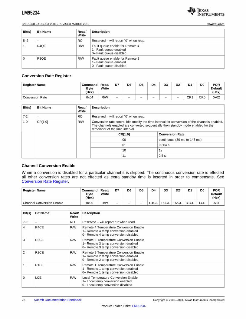
Bit(s) Bit Name Read/ DescriptionWrite
5–2 – RO Reserved – will report "0" when read.
1 R4QE R/W Fault queue enable for Remote 41– Fault queue enabled0– Fault queue disabled
0 R3QE R/W Fault queue enable for Remote 31– Fault queue enabled0– Fault queue disabled
Conversion Rate Register
Register Name Command Read/ D7 D6 D5 D4 D3 D2 D1 D0 PORByte Write Default(Hex) (Hex)
Conversion Rate 0x04 R/W – – – – – – CR1 CR0 0x02
Bit(s) Bit Name Read/ DescriptionWrite
7-2 – RO Reserved – will report "0" when read.
1-0 CR[1:0] R/W Conversion rate control bits modify the time interval for conversion of the channels enabled.The channels enabled are converted sequentially then standby mode enabled for theremainder of the time interval.
CR[1:0] Conversion Rate
00 continuous (30 ms to 143 ms)
01 0.364 s
10 1s
11 2.5 s
Channel Conversion Enable
When a conversion is disabled for a particular channel it is skipped. The continuous conversion rate is effectedall other conversion rates are not effected as extra standby time is inserted in order to compensate. SeeConversion Rate Register.
Register Name Command Read/ D7 D6 D5 D4 D3 D2 D1 D0 PORByte Write Default(Hex) (Hex)
Channel Conversion Enable 0x05 R/W – – – R4CE R3CE R2CE R1CE LCE 0x1F
Bit(s) Bit Name Read/ DescriptionWrite
7–5 – RO Reserved – will report "0" when read.
4 R4CE R/W Remote 4 Temperature Conversion Enable1– Remote 4 temp conversion enabled0– Remote 4 temp conversion disabled
3 R3CE R/W Remote 3 Temperature Conversion Enable1– Remote 3 temp conversion enabled0– Remote 3 temp conversion disabled
2 R2CE R/W Remote 2 Temperature Conversion Enable1– Remote 2 temp conversion enabled0– Remote 2 temp conversion disabled
1 R1CE R/W Remote 1 Temperature Conversion Enable1– Remote 1 temp conversion enabled0– Remote 1 temp conversion disabled
0 LCE R/W Local Temperature Conversion Enable1– Local temp conversion enabled0– Local temp conversion disabled
26 Submit Documentation Feedback Copyright © 2006–2013, Texas Instruments Incorporated
Product Folder Links: LM95234

LM95234
www.ti.com SNIS136D –AUGUST 2006–REVISED MARCH 2013
Filter Setting
Register Name Command Read/ D7 D6 D5 D4 D3 D2 D1 D0 PORByte Write Default(Hex) (Hex)
Filter Setting 0x06 R/W – – – – R2F1 R2F0 R1F1 R1F0 0x0F
Bit(s) Bit Name Read/ DescriptionWrite
7–4 – RO Reserved – will report "0" when read.
3–2 R2F[1:0] R/W Remote Channel 2 Filter Enable Bits
R2F[1:0] TEMPERATURE CONVERSIONSEQUENCE State
00 disable all digital filtering
01 enable basic filter
10 reserved (do not use)
11 enable enhanced filter
1–0 R1F[1:0] R/W Remote Channel 1 Filter Enable
R1F[1:0] Filter State
00 disable all digital filtering
01 enable basic filter
10 reserved (do not use)
11 enable enhanced filter
1-Shot
Register Name Command Read/ D7 D6 D5 D4 D3 D2 D1 D0 PORByte Write Default(Hex) (Hex)
1-Shot 0x0F WO – – – – – – – – –
Bit(s) Bit Name Read/ DescriptionWrite
7–0 - WO Writing to this register activates one conversion for all the enabled channels ifthe chip is in standby mode (i.e. standby bit = 1). The actual data written doesnot matter and is not stored.
STATUS REGISTERS
Common Status Register
Register Name Command Read/ D7 D6 D5 D4 D3 D2 D1 D0 PORByte Write Default(Hex) (Hex)
Common Status Register 0x02 RO BUSY NR – – SR4F SR3F SR2F SR1F 0x00
Bit(s) Bit Name Read/ DescriptionWrite
7 BUSY RO Busy bit (device converting)
6 NR RO Not Ready bit (30 ms), indicates power up initialization sequence is in progress
5–4 – RO Reserved – will report "0" when read.
3 SR4F RO Status Register 4 Flag:1 – indicates that Status Register 4 has at least one bit set0 – indicates that all of Status Register 4 bits are cleared
Copyright © 2006–2013, Texas Instruments Incorporated Submit Documentation Feedback 27
Product Folder Links: LM95234

LM95234
SNIS136D –AUGUST 2006–REVISED MARCH 2013 www.ti.com
Bit(s) Bit Name Read/ DescriptionWrite
2 SR3F RO Status Register 3 Flag:1 – indicates that Status Register 3 has at least one bit set0 – indicates that all of Status Register 3 bits are cleared
1 SR2F RO Status Register 2 Flag:1 – indicates that Status Register 2 has at least one bit set0 – indicates that all of Status Register 2 bits are cleared
0 SR1F RO Status Register 1 Flag:1 – indicates that Status Register 1 has at least one bit set0 – indicates that all of Status Register 1 bits are cleared
Status 1 Register (Diode Fault)
Status fault bits for open or shorted diode (i.e. Short Fault: D+ shorted to Ground or D-; Open Fault: D+ shortedto VDD, or floating). During fault conditions the temperature reading is 0 °C if unsigned value registers are read or–128.000 °C if signed value registers are read.
Register Name Command Read/ D7 D6 D5 D4 D3 D2 D1 D0 PORByte Write Default(Hex) (Hex)
Status 1 (Diode Fault) 0x07 RO R4DO R4DS R3DO R3DS R2DO R2DS R1DO R1DS –
Bit(s) Bit Name Read/ DescriptionWrite
7 R4DO RO Remote 4 diode open fault status:1 – indicates that remote 4 diode has an "open" fault0 – indicates that remote 4 diode does not have an "open" fault
6 R4DS RO Remote 4 diode short fault status:1 – indicates that remote 4 diode has a "short" fault0 – indicates that remote 4 diode does not have a "short" fault
5 R3DO RO Remote 3 diode open fault status:1 – indicates that remote 3 diode has an "open" fault0 – indicates that remote 3 diode does not have an "open" fault
4 R3DS RO Remote 3 diode short fault status:1 – indicates that remote 3 diode has a "short" fault0 – indicates that remote 3 diode does not have a "short" fault
3 R2DO RO Remote 2 diode open fault status:1 – indicates that remote 2 diode has an "open" fault0 – indicates that remote 2 diode does not have an "open" fault
2 R2DS RO Remote 2 diode short fault status:1 – indicates that remote 2 diode has a "short" fault0 – indicates that remote 2 diode does not have a "short" fault
1 R1DO RO Remote 1 diode open fault status:1 – indicates that remote 1 diode has an "open" fault0 – indicates that remote 1 diode does not have an "open" fault
0 R1DS RO Remote 1 diode short fault status:1 – indicates that remote 1 diode has a "short" fault0 – indicates that remote 1 diode does not have a "short" fault
Status 2 (TCRIT1)
Status bits for TCRIT1. When one or more of these bits are set and if not masked the TCRIT1 output willactivate. TCRIT1 will deactivate when all these bits are cleared.
Register Name Command Read/ D7 D6 D5 D4 D3 D2 D1 D0 PORByte Write Default(Hex) (Hex)
Status 2 (TCRIT1) 0x08 RO – – – R4T1 R3T1 R2T1 R1T1 LT1 –
28 Submit Documentation Feedback Copyright © 2006–2013, Texas Instruments Incorporated
Product Folder Links: LM95234

LM95234
www.ti.com SNIS136D –AUGUST 2006–REVISED MARCH 2013
Bit(s) Bit Name Read/ DescriptionWrite
7–5 - RO Reserved – will report "0" when read.
4 R4T1 RO Remote 4 Tcrit Status:1 – indicates that remote 4 reading is greater than or equal to the value set in Remote 4 Tcrit Limitregister0 – indicates that that remote 4 reading is less than the value set in Remote 4 Tcrit Limit registerminus the Common Hysteresis value
3 R3T1 RO Remote 3 Tcrit Status:1 – indicates that remote 3 reading is greater than or equal to the value set in Remote 3 Tcrit Limitregister0 – indicates that that remote 3 reading is less than the value set in Remote 3 Tcrit Limit registerminus the Common Hysteresis value
2 R2T1 RO Remote 2 Tcrit-1 Status:1 – indicates that remote 2 reading is greater than or equal to the value set in Remote 2 Tcrit-1Limit register0 – indicates that that remote 2 reading is less than the value set in Remote 2 Tcrit-1 Limit registerminus the Common Hysteresis value
1 R1T1 RO Remote 1 Tcrit-1 Status:1 – indicates that remote 1 reading is greater than or equal to the value set in Remote 1 Tcrit-1Limit register0 – indicates that that remote 1 reading is less than the value set in Remote 1 Tcrit-1 Limit registerminus the Common Hysteresis value
0 LT1 RO Local Tcrit Status:1 – indicates that local reading is greater than or equal to the value set in Local Tcrit Limit register0 – indicates that local reading is less than the value set in Local Tcrit Limit register minus theCommon Hysteresis value
Status 3 (TCRIT2)
Status bits for TCRIT2. When one or more of these bits are set and if not masked the TCRIT2 output willactivate. TCRIT2 will deactivate when all these bits are cleared.
Register Name Command Read/ D7 D6 D5 D4 D3 D2 D1 D0 PORByte Write Default(Hex) (Hex)
Status 3 (TCRIT2) 0x09 RO – – – R4T2 R3T2 R2T2 R1T2 LT2 –
Bit(s) Bit Name Read/ DescriptionWrite
7–5 - RO Reserved – will report "0" when read.
4 R4T2 RO Remote 4 Tcrit Status:1 – indicates that remote 4 reading is greater than or equal to the value set in Remote 4 Tcrit Limitregister0 – indicates that that remote 4 reading is less than the value set in Remote 4 Tcrit Limit registerminus the Common Hysteresis value
3 R3T2 RO Remote 3 Tcrit Status:1 – indicates that remote 3 reading is greater than or equal to the value set in Remote 3 Tcrit Limitregister0 – indicates that that remote 3 reading is less than the value set in Remote 3 Tcrit Limit registerminus the Common Hysteresis value
2 R2T2 RO Remote 2 Tcrit-2 Status:1 – indicates that remote 2 reading is greater than or equal to the value set in Remote 2 Tcrit-2Limit register0 – indicates that that remote 2 reading is less than the value set in Remote 2 Tcrit-2 Limit registerminus the Common Hysteresis value
1 R1T2 RO Remote 1 Tcrit-2 Status:1 – indicates that remote 1 reading is greater than or equal to the value set in Remote 1 Tcrit-2Limit register0 – indicates that that remote 1 reading is less than the value set in Remote 1 Tcrit-2 Limit registerminus the Common Hysteresis value
Copyright © 2006–2013, Texas Instruments Incorporated Submit Documentation Feedback 29
Product Folder Links: LM95234

LM95234
SNIS136D –AUGUST 2006–REVISED MARCH 2013 www.ti.com
Bit(s) Bit Name Read/ DescriptionWrite
0 LT2 RO Local Tcrit Status:1 – indicates that local reading is greater than or equal to the value set in Local Tcrit Limit register0 – indicates that local reading is less than the value set in Local Tcrit Limit register minus theCommon Hysteresis value
Status 4 (TCRIT3)
Status bits for TCRIT3. When one or more of these bits are set and if not masked the TCRIT3 output willactivate. TCRIT3 will deactivate when all these bits are cleared.
Register Name Command Read/ D7 D6 D5 D4 D3 D2 D1 D0 PORByte Write Default(Hex) (Hex)
Status 4 (TCRIT3) 0x0A RO – – – R4T3 R3T3 R2T3 R1T3 LT3 –
Bit(s) Bit Name Read/ DescriptionWrite
7–5 - RO Reserved – will report "0" when read.
4 R4T3 RO Remote 4 Tcrit Status:1 – indicates that remote 4 reading is greater than or equal to the value set in Remote 4 Tcrit Limitregister0 – indicates that that remote 4 reading is less than the value set in Remote 4 Tcrit Limit registerminus the Common Hysteresis value
3 R3T3 RO Remote 3 Tcrit Status:1 – indicates that remote 3 reading is greater than or equal to the value set in Remote 3 Tcrit Limitregister0 – indicates that that remote 3 reading is less than the value set in Remote 3 Tcrit Limit registerminus the Common Hysteresis value
2 R2T3 RO Remote 2 Tcrit-2 Status:1 – indicates that remote 2 reading is greater than or equal to the value set in Remote 2 Tcrit-2Limit register0 – indicates that that remote 2 reading is less than the value set in Remote 2 Tcrit-2 Limit registerminus the Common Hysteresis value
1 R1T3 RO Remote 1 Tcrit-2 Status:1 – indicates that remote 1 reading is greater than or equal to the value set in Remote 1 Tcrit-2Limit register0 – indicates that that remote 1 reading is less than the value set in Remote 1 Tcrit-2 Limit registerminus the Common Hysteresis value
0 LT3 RO Local Tcrit Status:1 – indicates that local reading is greater than or equal to the value set in Local Tcrit Limit register0 – indicates that local reading is less than the value set in Local Tcrit Limit register minus theCommon Hysteresis value
Diode Model Status
Register Name Command Read/ D7 D6 D5 D4 D3 D2 D1 D0 PORByte Write Default(Hex) (Hex)
Diode Model Status (TruTherm on and 0x38 RO – – – R4TD R3TD R2TD R1TD – –3904 connected)
Bit(s) Bit Name Read/ DescriptionWrite
7-5 – RO Reserved – will report "0" when read.
4 R4TD RO Remote 4 TruTherm BJT beta compensation on and 3904 detect:1 – indicates that for channel 4 TruTherm is ON and 3904 connected0 – indicates proper operation
3 R3TD RO Remote 3 TruTherm BJT beta compensation on and 3904 detect:1 – indicates that for channel 3 TruTherm is ON and 3904 connected0 – indicates proper operation
30 Submit Documentation Feedback Copyright © 2006–2013, Texas Instruments Incorporated
Product Folder Links: LM95234
LM95234
www.ti.com SNIS136D –AUGUST 2006–REVISED MARCH 2013
Bit(s) Bit Name Read/ DescriptionWrite
2 R2TD RO Remote 2 TruTherm BJT beta compensation on and 3904 detect:1 – indicates that for channel 2 TruTherm is ON and 3904 connected0 – indicates proper operation
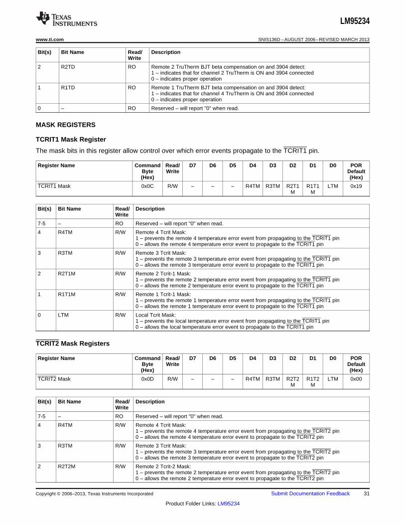
1 R1TD RO Remote 1 TruTherm BJT beta compensation on and 3904 detect:1 – indicates that for channel 4 TruTherm is ON and 3904 connected0 – indicates proper operation
0 – RO Reserved – will report "0" when read.
MASK REGISTERS
TCRIT1 Mask Register
The mask bits in this register allow control over which error events propagate to the TCRIT1 pin.
Register Name Command Read/ D7 D6 D5 D4 D3 D2 D1 D0 PORByte Write Default(Hex) (Hex)
TCRIT1 Mask 0x0C R/W – – – R4TM R3TM R2T1 R1T1 LTM 0x19M M
Bit(s) Bit Name Read/ DescriptionWrite
7-5 – RO Reserved – will report "0" when read.
4 R4TM R/W Remote 4 Tcrit Mask:1 – prevents the remote 4 temperature error event from propagating to the TCRIT1 pin0 – allows the remote 4 temperature error event to propagate to the TCRIT1 pin
3 R3TM R/W Remote 3 Tcrit Mask:1 – prevents the remote 3 temperature error event from propagating to the TCRIT1 pin0 – allows the remote 3 temperature error event to propagate to the TCRIT1 pin
2 R2T1M R/W Remote 2 Tcrit-1 Mask:1 – prevents the remote 2 temperature error event from propagating to the TCRIT1 pin0 – allows the remote 2 temperature error event to propagate to the TCRIT1 pin
1 R1T1M R/W Remote 1 Tcrit-1 Mask:1 – prevents the remote 1 temperature error event from propagating to the TCRIT1 pin0 – allows the remote 1 temperature error event to propagate to the TCRIT1 pin
0 LTM R/W Local Tcrit Mask:1 – prevents the local temperature error event from propagating to the TCRIT1 pin0 – allows the local temperature error event to propagate to the TCRIT1 pin
TCRIT2 Mask Registers
Register Name Command Read/ D7 D6 D5 D4 D3 D2 D1 D0 PORByte Write Default(Hex) (Hex)
TCRIT2 Mask 0x0D R/W – – – R4TM R3TM R2T2 R1T2 LTM 0x00M M
Bit(s) Bit Name Read/ DescriptionWrite
7-5 – RO Reserved – will report "0" when read.
4 R4TM R/W Remote 4 Tcrit Mask:1 – prevents the remote 4 temperature error event from propagating to the TCRIT2 pin0 – allows the remote 4 temperature error event to propagate to the TCRIT2 pin
3 R3TM R/W Remote 3 Tcrit Mask:1 – prevents the remote 3 temperature error event from propagating to the TCRIT2 pin0 – allows the remote 3 temperature error event to propagate to the TCRIT2 pin
2 R2T2M R/W Remote 2 Tcrit-2 Mask:1 – prevents the remote 2 temperature error event from propagating to the TCRIT2 pin0 – allows the remote 2 temperature error event to propagate to the TCRIT2 pin
Copyright © 2006–2013, Texas Instruments Incorporated Submit Documentation Feedback 31
Product Folder Links: LM95234

LM95234
SNIS136D –AUGUST 2006–REVISED MARCH 2013 www.ti.com
Bit(s) Bit Name Read/ DescriptionWrite
1 R1T2M R/W Remote 1 Tcrit-2 Mask:1 – prevents the remote 1 temperature error event from propagating to the TCRIT2 pin0 – allows the remote 1 temperature error event to propagate to the TCRIT2 pin
0 LTM R/W Local Tcrit Mask:1 – prevents the local temperature error event from propagating to the TCRIT2 pin0 – allows the local temperature error event to propagate to the TCRIT2 pin
TCRIT3 Mask Register
The mask bits in this register allow control over which error events propagate to the TCRIT3 pin.
Register Name Command Read/ D7 D6 D5 D4 D3 D2 D1 D0 PORByte Write Default(Hex) (Hex)
TCRIT3 Mask 0x0E R/W – – – R4TM R3TM R2T2 R1T2 LTM 0x07M M
Bit(s) Bit Name Read/ DescriptionWrite
7-5 – RO Reserved – will report "0" when read.
4 R4TM R/W Remote 4 Tcrit Mask:1 – prevents the remote 4 temperature error event from propagating to the TCRIT3 pin0 – allows the remote 4 temperature error event to propagate to the TCRIT3 pin
3 R3TM R/W Remote 3 Tcrit Mask:1 – prevents the remote 3 temperature error event from propagating to the TCRIT3 pin0 – allows the remote 3 temperature error event to propagate to the TCRIT3 pin
2 R2T2M R/W Remote 2 Tcrit-2 Mask:1 – prevents the remote 2 temperature error event from propagating to the TCRIT3 pin0 – allows the remote 2 temperature error event to propagate to the TCRIT3 pin
1 R1T2M R/W Remote 1 Tcrit-2 Mask:1 – prevents the remote 1 temperature error event from propagating to the TCRIT3 pin0 – allows the remote 1 temperature error event to propagate to the TCRIT3 pin
0 LTM R/W Local Tcrit Mask:1 – prevents the local temperature error event from propagating to the TCRIT3 pin0 – allows the local temperature error event to propagate to the TCRIT3 pin
LIMIT REGISTERS
Local Limit Register
The Local Limit register range is 0°C to 127°C. The value programmed in this register is used to determine alocal temperature error event.
Register Name Command Read/ D7 D6 D5 D4 D3 D2 D1 D0 PORByte Write Default(Hex) (Hex)
Local Tcrit Limit 0x40 R/W 0 64 32 16 8 4 2 1 0x55
Bit(s) Bit Name Read/ DescriptionWrite
7 0 R0 Read only bit will always report "0".
6 64 R/W bit weight 64°C
5 32 R/W bit weight 32°C
4 16 R/W bit weight 16°C
3 8 R/W bit weight 8°C
2 4 R/W bit weight 4°C
1 2 R/W bit weight 2°C
32 Submit Documentation Feedback Copyright © 2006–2013, Texas Instruments Incorporated
Product Folder Links: LM95234

LM95234
www.ti.com SNIS136D –AUGUST 2006–REVISED MARCH 2013
Bit(s) Bit Name Read/ DescriptionWrite
0 1 R/W bit weight 1°C
Remote Limit Registers
The range for these registers is 0°C to 255°C.
Register Name Command Read/ D7 D6 D5 D4 D3 D2 D1 D0 PORByte Write Default(Hex) (Hex)
Remote 1 Tcrit-1 Limit (used by 0x41 R/W 128 64 32 16 8 4 2 1 0x6ETCRIT1 error events)
Remote 2 Tcrit-1 Limit (used by 0x42 R/W 128 64 32 16 8 4 2 1 0x6ETCRIT1 error events)
Remote 3 Tcrit Limit (used by TCRIT1, 0x43 R/W 128 64 32 16 8 4 2 1 0x55TCRIT2 and TCRIT3 error events)
Remote 4 Tcrit Limit (used by TCRIT1, 0x44 R/W 128 64 32 16 8 4 2 1 0x55TCRIT2 and TCRIT3 error events)
Remote 1 Tcrit-2 and Tcrit3 Limit (used 0x49 R/W 128 64 32 16 8 4 2 1 0x55by TCRIT2 and TCRIT3 error events)
Remote 2 Tcrit-2 and Tcrit3 Limit (used 0x4A R/W 128 64 32 16 8 4 2 1 0x55by TCRIT2 and TCRIT3 error events)
Bit(s) Bit Name Read/ DescriptionWrite
7 128 R/W bit weight 128°C
6 64 R/W bit weight 64°C
5 32 R/W bit weight 32°C
4 16 R/W bit weight 16°C
3 8 R/W bit weight 8°C
2 4 R/W bit weight 4°C
1 2 R/W bit weight 2°C
0 1 R/W bit weight 1°C
Table 9. Limit assignments for each TCRIT output pin:
Output Pin Remote 4 Remote 3 Remote 2 Remote 1 Local
TCRIT1 Remote 4 Tcrit Limit Remote 3 Tcrit Limit Remote 2 Tcrit-1 Remote 1 Tcrit-1 Local Tcrit LimitLimit Limit
TCRIT2 Remote 4 Tcrit Limit Remote 3 Tcrit Limit Remote 2 Tcrit-2 Remote 1 Tcrit-2 Local Tcrit LimitLimit Limit
TCRIT3 Remote 4 Tcrit Limit Remote 3 Tcrit Limit Remote 2 Tcrit-2 Remote 1 Tcrit-2 Local Tcrit LimitLimit Limit
Common Tcrit Hysteresis Register
The hysteresis register range is 0°C to 32°C. The value programmed in this register is used to modify all the limitvalues for decreasing temperature.
Register Name Command Read/ D7 D6 D5 D4 D3 D2 D1 D0 PORByte Write Default(Hex) (Hex)
Common Tcrit Hysteresis 0x5A R/W 0 0 0 16 8 4 2 1 0x0A
Copyright © 2006–2013, Texas Instruments Incorporated Submit Documentation Feedback 33
Product Folder Links: LM95234

qkT
=tV
FI = IxK tVBEV
©§
¹·
S x e««¬
ª
»»¼
º-1
LM95234
SNIS136D –AUGUST 2006–REVISED MARCH 2013 www.ti.com
Bit(s) Bit Name Read/ DescriptionWrite
7 0 RO Read only bit will always report "0".
6 0 RO Read only bit will always report "0".
5 0 RO Read only bit will always report "0".
4 16 R/W bit weight 16°C
3 8 R/W bit weight 8°C
2 4 R/W bit weight 4°C
1 2 R/W bit weight 2°C
0 1 R/W bit weight 1°C
IDENTIFICATION REGISTERS
Register Name Command Read/ D7 D6 D5 D4 D3 D2 D1 D0 PORByte Write Default(Hex) (Hex)
Manufacturer ID 0xFE RO 0 0 0 0 0 0 0 1 0x01
Revision ID 0xFF RO 0 1 1 1 1 0 0 1 0x79
Applications Hints
The LM95234 can be applied easily in the same way as other integrated-circuit temperature sensors, and itsremote diode sensing capability allows it to be used in new ways as well. It can be soldered to a printed circuitboard, and because the path of best thermal conductivity is between the die and the pins, its temperature willeffectively be that of the printed circuit board lands and traces soldered to the LM95234's pins. This presumesthat the ambient air temperature is almost the same as the surface temperature of the printed circuit board; if theair temperature is much higher or lower than the surface temperature, the actual temperature of the LM95234 diewill be at an intermediate temperature between the surface and air temperatures. Again, the primary thermalconduction path is through the leads, so the circuit board temperature will contribute to the die temperature muchmore strongly than will the air temperature.
To measure temperature external to the LM95234's die, incorporates remote diode sensing technology. Thisdiode can be located on the die of a target IC, allowing measurement of the IC's temperature, independent of theLM95234's temperature. A discrete diode can also be used to sense the temperature of external objects orambient air. Remember that a discrete diode's temperature will be affected, and often dominated, by thetemperature of its leads. Most silicon diodes do not lend themselves well to this application. It is recommendedthat an MMBT3904 transistor base emitter junction be used with the collector tied to the base.
The LM95234’s TruTherm BJT beta compensation technology allows accurate sensing of integrated thermaldiodes, such as those found on most processors. With TruTherm technology turned off, the LM95234 canmeasure a diode-connected transistor such as the MMBT3904 or the thermal diode found in an AMD processor.
The LM95234 has been optimized to measure the remote thermal diode integrated in a typical Intel processor on65 nm or 90 nm process or an MMBT3904 transistor. Using the Remote Diode Model Select register any of thefour remote inputs can be optimized for a typical Intel processor on 65 nm or 90 nm process or an MMBT3904.
DIODE NON-IDEALITY
Diode Non-Ideality Factor Effect on Accuracy
When a transistor is connected as a diode, the following relationship holds for variables VBE, T and IF:
where
•• q = 1.6×10⁻¹⁹ Coulombs (the electron charge),
34 Submit Documentation Feedback Copyright © 2006–2013, Texas Instruments Incorporated
Product Folder Links: LM95234

MMBT3904
LM95234
100 pF
PROCESSOR
ICIR
IE = IF
100 pF
7
6
D1+
D2+
5D-
IF
IR
=Tq x ' BEV
x kK x ln ¸¹
ᬩ
§ I 2C
I 1C
¸¹
ᬩ
§T =
q x 'VBE
K x k x lnIF2
IF1
¹·
©§x
¹·
©§x=' lnBE I
I
qkT
V K2F
1F
FI = IxK tVBEV
©§
¹·
S x e««¬
ª
»»¼
º
LM95234
www.ti.com SNIS136D –AUGUST 2006–REVISED MARCH 2013
• T = Absolute Temperature in Kelvin• k = 1.38×10⁻²³ joules/K (Boltzmann's constant),• η is the non-ideality factor of the process the diode is manufactured on,• IS = Saturation Current and is process dependent,• If = Forward Current through the base-emitter junction• VBE = Base-Emitter Voltage drop (1)
In the active region, the -1 term is negligible and may be eliminated, yielding the following equation
(2)
In Equation 2, η and IS are dependant upon the process that was used in the fabrication of the particular diode.By forcing two currents with a very controlled ratio(IF2 / IF1) and measuring the resulting voltage difference, it ispossible to eliminate the IS term. Solving for the forward voltage difference yields the relationship:
(3)
Solving Equation 3 for temperature yields:
(4)
Equation 4 holds true when a diode connected transistor such as the MMBT3904 is used. When this “diode”equation is applied to an integrated diode such as a processor transistor with its collector tied to GND as shownin Figure 23 it will yield a wide non-ideality spread. This wide non-ideality spread is not due to true processvariation but due to the fact that Equation 4 is an approximation.
TruTherm BJT beta compensation technology uses the transistor equation, Equation 5, which is a more accuraterepresentation of the topology of the thermal diode found in an FPGA or processor.
(5)
Figure 23. Thermal Diode Current Paths
TruTherm should only be enabled when measuring the temperature of a transistor integrated as shown in theprocessor of Figure 23, because Equation 5 only applies to this topology.
Copyright © 2006–2013, Texas Instruments Incorporated Submit Documentation Feedback 35
Product Folder Links: LM95234

x PCBR¸¹
·:62.0=ERT Cº
¨©
§
LM95234
SNIS136D –AUGUST 2006–REVISED MARCH 2013 www.ti.com
Calculating Total System Accuracy
The voltage seen by the LM95234 also includes the IFRS voltage drop of the series resistance. The non-idealityfactor, η, is the only other parameter not accounted for and depends on the diode that is used for measurement.Since ΔVBE is proportional to both η and T, the variations in η cannot be distinguished from variations intemperature. Since the non-ideality factor is not controlled by the temperature sensor, it will directly add to theinaccuracy of the sensor. For the for Intel processor on 65 nm process, Intel specifies a +4.06%/−0.897%variation in η from part to part when the processor diode is measured by a circuit that assumes diode equation,Equation 4, as true. As an example, assume a temperature sensor has an accuracy specification of ±1.0°C at atemperature of 80°C (353 Kelvin) and the processor diode has a non-ideality variation of +1.19%/−0.27%. Theresulting system accuracy of the processor temperature being sensed will be:
TACC = + 1.0°C + (+4.06% of 353 K) = +15.3 °C (6)
andTACC = - 1.0°C + (−0.89% of 353 K) = −4.1 °C (7)
TrueTherm technology uses the transistor equation, Equation 4, resulting in a non-ideality spread that trulyreflects the process variation which is very small. The transistor equation non-ideality spread is ±0.39% for theIntel processor on 90 nm process. The resulting accuracy when using TruTherm BJT beta compensationtechnology improves to:
TACC = ±0.75°C + (±0.39% of 353 K) = ± 2.16 °C (8)
The next error term to be discussed is that due to the series resistance of the thermal diode and printed circuitboard traces. The thermal diode series resistance is specified on most processor data sheets. For Intelprocessors in 65 nm process, this is specified at 4.52Ω typical. The LM95234 accommodates the typical seriesresistance of Intel Processor on 65 nm process. The error that is not accounted for is the spread of theprocessor's series resistance, that is 2.79Ω to 6.24Ω or ±1.73Ω. The equation to calculate the temperature errordue to series resistance (TER) for the LM95234 is simply:
(9)
Solving Equation 9 for RPCB equal to ±1.73Ω results in the additional error due to the spread in the seriesresistance of ±1.07°C. The spread in error cannot be canceled out, as it would require measuring each individualthermal diode device. This is quite difficult and impractical in a large volume production environment.
Equation 9 can also be used to calculate the additional error caused by series resistance on the printed circuitboard. Since the variation of the PCB series resistance is minimal, the bulk of the error term is always positiveand can simply be cancelled out by subtracting it from the output readings of the LM95234.
36 Submit Documentation Feedback Copyright © 2006–2013, Texas Instruments Incorporated
Product Folder Links: LM95234
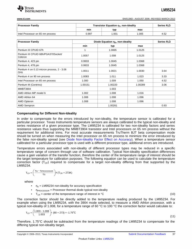
TCF = (80 + 273) = -1.75oC1.003 - 1.0081.003 ¹
ᩤ
TCF = (TCR + 273K)xKS - KPROCESSOR
KS ¹·
©§
LM95234
www.ti.com SNIS136D –AUGUST 2006–REVISED MARCH 2013
Processor Family Transistor Equation ηT, non-ideality Series R,Ωmin typ max
Intel Processor on 65 nm process 0.997 1.001 1.005 4.52
Processor Family Diode Equation ηD, non-ideality Series R,Ωmin typ max
Pentium III CPUID 67h 1 1.0065 1.0125
Pentium III CPUID 68h/PGA370Socket/ 1.0057 1.008 1.0125Celeron
Pentium 4, 423 pin 0.9933 1.0045 1.0368
Pentium 4, 478 pin 0.9933 1.0045 1.0368
Pentium 4 on 0.13 micron process, 2 - 3.06 1.0011 1.0021 1.0030 3.64GHz
Pentium 4 on 90 nm process 1.0083 1.011 1.023 3.33
Intel Processor on 65 nm process 1.000 1.009 1.050 4.52
Pentium M (Centrino) 1.00151 1.00220 1.00289 3.06
MMBT3904 1.003
AMD Athlon MP model 6 1.002 1.008 1.016
AMD Athlon 64 1.008 1.008 1.096
AMD Opteron 1.008 1.008 1.096
AMD Sempron 1.00261 0.93
Compensating for Different Non-Ideality
In order to compensate for the errors introduced by non-ideality, the temperature sensor is calibrated for aparticular processor. Texas Instruments temperature sensors are always calibrated to the typical non-ideality andseries resistance of a given processor type. The LM95234 is calibrated for two non-ideality factors and seriesresistance values thus supporting the MMBT3904 transistor and Intel processors on 65 nm process without therequirement for additional trims. For most accurate measurements TruTherm BJT beta compensation modeshould be turned on when measuring the Intel processor on 65 nm process to minimize the error introduced bythe false non-ideality spread (see Diode Non-Ideality Factor Effect on Accuracy). When a temperature sensorcalibrated for a particular processor type is used with a different processor type, additional errors are introduced.
Temperature errors associated with non-ideality of different processor types may be reduced in a specifictemperature range of concern through use of software calibration. Typical Non-ideality specification differencescause a gain variation of the transfer function, therefore the center of the temperature range of interest should bethe target temperature for calibration purposes. The following equation can be used to calculate the temperaturecorrection factor (TCF) required to compensate for a target non-ideality differing from that supported by theLM95234.
where• ηS = LM95234 non-ideality for accuracy specification• ηPROCESSOR = Processor thermal diode typical non-ideality• TCR = center of the temperature range of interest in °C (10)
The correction factor should be directly added to the temperature reading produced by the LM95234. Forexample when using the LM95234, with the 3904 mode selected, to measure a AMD Athlon processor, with atypical non-ideality of 1.008, for a temperature range of 60 °C to 100 °C the correction factor would calculate to:
(11)
Therefore, 1.75°C should be subtracted from the temperature readings of the LM95234 to compensate for thediffering typical non-ideality target.
Copyright © 2006–2013, Texas Instruments Incorporated Submit Documentation Feedback 37
Product Folder Links: LM95234

LM95234
SNIS136D –AUGUST 2006–REVISED MARCH 2013 www.ti.com
PCB LAYOUT FOR MINIMIZING NOISE
Figure 24. Ideal Diode Trace Layout
In a noisy environment, such as a processor mother board, layout considerations are very critical. Noise inducedon traces running between the remote temperature diode sensor and the LM95234 can cause temperatureconversion errors. Keep in mind that the signal level the LM95234 is trying to measure is in microvolts. Thefollowing guidelines should be followed:1. VDD should be bypassed with a 0.1 µF capacitor in parallel with 100 pF. The 100 pF capacitor should be
placed as close as possible to the power supply pin. A bulk capacitance of approximately 10 µF needs to bein the near vicinity of the LM95234.
2. A 100 pF diode bypass capacitor is recommended to filter high frequency noise but may not be necessary.Make sure the traces to the 100 pF capacitor are matched. Place the filter capacitors close to the LM95234pins.
3. Ideally, the LM95234 should be placed within 10 cm of the Processor diode pins with the traces being asstraight, short and identical as possible. Trace resistance of 1Ω can cause as much as 0.62°C of error. Thiserror can be compensated by using simple software offset compensation.
4. Diode traces should be surrounded by a GND guard ring to either side, above and below if possible. ThisGND guard should not be between the D+ and D− lines. In the event that noise does couple to the diodelines it would be ideal if it is coupled common mode. That is equally to the D+ and D− lines.
5. Avoid routing diode traces in close proximity to power supply switching or filtering inductors.6. Avoid running diode traces close to or parallel to high speed digital and bus lines. Diode traces should be
kept at least 2 cm apart from the high speed digital traces.7. If it is necessary to cross high speed digital traces, the diode traces and the high speed digital traces should
cross at a 90 degree angle.8. The ideal place to connect the LM95234's GND pin is as close as possible to the Processors GND
associated with the sense diode.9. Leakage current between D+ and GND and between D+ and D− should be kept to a minimum. Thirteen
nano-amperes of leakage can cause as much as 0.2°C of error in the diode temperature reading. Keepingthe printed circuit board as clean as possible will minimize leakage current.
Noise coupling into the digital lines greater than 400 mVp-p (typical hysteresis) and undershoot less than 500 mVbelow GND, may prevent successful SMBus communication with the LM95234. SMBus no acknowledge is themost common symptom, causing unnecessary traffic on the bus. Although the SMBus maximum frequency ofcommunication is rather low (100 kHz max), care still needs to be taken to ensure proper termination within asystem with multiple parts on the bus and long printed circuit board traces. An RC lowpass filter with a 3 dBcorner frequency of about 40 MHz is included on the LM95234's SMBCLK input. Additional resistance can beadded in series with the SMBDAT and SMBCLK lines to further help filter noise and ringing. Minimize noisecoupling by keeping digital traces out of switching power supply areas as well as ensuring that digital linescontaining high speed data communications cross at right angles to the SMBDAT and SMBCLK lines.
38 Submit Documentation Feedback Copyright © 2006–2013, Texas Instruments Incorporated
Product Folder Links: LM95234

LM95234
www.ti.com SNIS136D –AUGUST 2006–REVISED MARCH 2013
REVISION HISTORY
Changes from Revision C (March 2013) to Revision D Page
• Changed layout of National Data Sheet to TI format .......................................................................................................... 38
Copyright © 2006–2013, Texas Instruments Incorporated Submit Documentation Feedback 39
Product Folder Links: LM95234

PACKAGE OPTION ADDENDUM
www.ti.com 7-Oct-2013
Addendum-Page 1
PACKAGING INFORMATION
Orderable Device Status(1)
Package Type PackageDrawing
Pins PackageQty
Eco Plan(2)
Lead/Ball Finish MSL Peak Temp(3)
Op Temp (°C) Device Marking(4/5)
Samples
LM95234CISD/NOPB ACTIVE WSON NHL 14 1000 Green (RoHS& no Sb/Br)
CU SN Level-1-260C-UNLIM -40 to 140 95234CI
LM95234CISDX/NOPB ACTIVE WSON NHL 14 4500 Green (RoHS& no Sb/Br)
CU SN Level-1-260C-UNLIM -40 to 140 95234CI
(1) The marketing status values are defined as follows:ACTIVE: Product device recommended for new designs.LIFEBUY: TI has announced that the device will be discontinued, and a lifetime-buy period is in effect.NRND: Not recommended for new designs. Device is in production to support existing customers, but TI does not recommend using this part in a new design.PREVIEW: Device has been announced but is not in production. Samples may or may not be available.OBSOLETE: TI has discontinued the production of the device.
(2) Eco Plan - The planned eco-friendly classification: Pb-Free (RoHS), Pb-Free (RoHS Exempt), or Green (RoHS & no Sb/Br) - please check http://www.ti.com/productcontent for the latest availabilityinformation and additional product content details.TBD: The Pb-Free/Green conversion plan has not been defined.Pb-Free (RoHS): TI's terms "Lead-Free" or "Pb-Free" mean semiconductor products that are compatible with the current RoHS requirements for all 6 substances, including the requirement thatlead not exceed 0.1% by weight in homogeneous materials. Where designed to be soldered at high temperatures, TI Pb-Free products are suitable for use in specified lead-free processes.Pb-Free (RoHS Exempt): This component has a RoHS exemption for either 1) lead-based flip-chip solder bumps used between the die and package, or 2) lead-based die adhesive used betweenthe die and leadframe. The component is otherwise considered Pb-Free (RoHS compatible) as defined above.Green (RoHS & no Sb/Br): TI defines "Green" to mean Pb-Free (RoHS compatible), and free of Bromine (Br) and Antimony (Sb) based flame retardants (Br or Sb do not exceed 0.1% by weightin homogeneous material)
(3) MSL, Peak Temp. -- The Moisture Sensitivity Level rating according to the JEDEC industry standard classifications, and peak solder temperature.
(4) There may be additional marking, which relates to the logo, the lot trace code information, or the environmental category on the device.
(5) Multiple Device Markings will be inside parentheses. Only one Device Marking contained in parentheses and separated by a "~" will appear on a device. If a line is indented then it is a continuationof the previous line and the two combined represent the entire Device Marking for that device.
Important Information and Disclaimer:The information provided on this page represents TI's knowledge and belief as of the date that it is provided. TI bases its knowledge and belief on informationprovided by third parties, and makes no representation or warranty as to the accuracy of such information. Efforts are underway to better integrate information from third parties. TI has taken andcontinues to take reasonable steps to provide representative and accurate information but may not have conducted destructive testing or chemical analysis on incoming materials and chemicals.TI and TI suppliers consider certain information to be proprietary, and thus CAS numbers and other limited information may not be available for release.
In no event shall TI's liability arising out of such information exceed the total purchase price of the TI part(s) at issue in this document sold by TI to Customer on an annual basis.

TAPE AND REEL INFORMATION
*All dimensions are nominal
Device PackageType
PackageDrawing
Pins SPQ ReelDiameter
(mm)
ReelWidth
W1 (mm)
A0(mm)
B0(mm)
K0(mm)
P1(mm)
W(mm)
Pin1Quadrant
LM95234CISD/NOPB WSON NHL 14 1000 178.0 12.4 4.3 4.3 1.3 8.0 12.0 Q1
LM95234CISDX/NOPB WSON NHL 14 4500 330.0 12.4 4.3 4.3 1.3 8.0 12.0 Q1
PACKAGE MATERIALS INFORMATION
www.ti.com 23-Sep-2013
Pack Materials-Page 1

*All dimensions are nominal
Device Package Type Package Drawing Pins SPQ Length (mm) Width (mm) Height (mm)
LM95234CISD/NOPB WSON NHL 14 1000 210.0 185.0 35.0
LM95234CISDX/NOPB WSON NHL 14 4500 367.0 367.0 35.0
PACKAGE MATERIALS INFORMATION
www.ti.com 23-Sep-2013
Pack Materials-Page 2

MECHANICAL DATA
NHL0014B
www.ti.com
SDA14B (Rev A)

IMPORTANT NOTICE
Texas Instruments Incorporated and its subsidiaries (TI) reserve the right to make corrections, enhancements, improvements and otherchanges to its semiconductor products and services per JESD46, latest issue, and to discontinue any product or service per JESD48, latestissue. Buyers should obtain the latest relevant information before placing orders and should verify that such information is current andcomplete. All semiconductor products (also referred to herein as “components”) are sold subject to TI’s terms and conditions of salesupplied at the time of order acknowledgment.TI warrants performance of its components to the specifications applicable at the time of sale, in accordance with the warranty in TI’s termsand conditions of sale of semiconductor products. Testing and other quality control techniques are used to the extent TI deems necessaryto support this warranty. Except where mandated by applicable law, testing of all parameters of each component is not necessarilyperformed.TI assumes no liability for applications assistance or the design of Buyers’ products. Buyers are responsible for their products andapplications using TI components. To minimize the risks associated with Buyers’ products and applications, Buyers should provideadequate design and operating safeguards.TI does not warrant or represent that any license, either express or implied, is granted under any patent right, copyright, mask work right, orother intellectual property right relating to any combination, machine, or process in which TI components or services are used. Informationpublished by TI regarding third-party products or services does not constitute a license to use such products or services or a warranty orendorsement thereof. Use of such information may require a license from a third party under the patents or other intellectual property of thethird party, or a license from TI under the patents or other intellectual property of TI.Reproduction of significant portions of TI information in TI data books or data sheets is permissible only if reproduction is without alterationand is accompanied by all associated warranties, conditions, limitations, and notices. TI is not responsible or liable for such altereddocumentation. Information of third parties may be subject to additional restrictions.Resale of TI components or services with statements different from or beyond the parameters stated by TI for that component or servicevoids all express and any implied warranties for the associated TI component or service and is an unfair and deceptive business practice.TI is not responsible or liable for any such statements.Buyer acknowledges and agrees that it is solely responsible for compliance with all legal, regulatory and safety-related requirementsconcerning its products, and any use of TI components in its applications, notwithstanding any applications-related information or supportthat may be provided by TI. Buyer represents and agrees that it has all the necessary expertise to create and implement safeguards whichanticipate dangerous consequences of failures, monitor failures and their consequences, lessen the likelihood of failures that might causeharm and take appropriate remedial actions. Buyer will fully indemnify TI and its representatives against any damages arising out of the useof any TI components in safety-critical applications.In some cases, TI components may be promoted specifically to facilitate safety-related applications. With such components, TI’s goal is tohelp enable customers to design and create their own end-product solutions that meet applicable functional safety standards andrequirements. Nonetheless, such components are subject to these terms.No TI components are authorized for use in FDA Class III (or similar life-critical medical equipment) unless authorized officers of the partieshave executed a special agreement specifically governing such use.Only those TI components which TI has specifically designated as military grade or “enhanced plastic” are designed and intended for use inmilitary/aerospace applications or environments. Buyer acknowledges and agrees that any military or aerospace use of TI componentswhich have not been so designated is solely at the Buyer's risk, and that Buyer is solely responsible for compliance with all legal andregulatory requirements in connection with such use.TI has specifically designated certain components as meeting ISO/TS16949 requirements, mainly for automotive use. In any case of use ofnon-designated products, TI will not be responsible for any failure to meet ISO/TS16949.
Products ApplicationsAudio www.ti.com/audio Automotive and Transportation www.ti.com/automotiveAmplifiers amplifier.ti.com Communications and Telecom www.ti.com/communicationsData Converters dataconverter.ti.com Computers and Peripherals www.ti.com/computersDLP® Products www.dlp.com Consumer Electronics www.ti.com/consumer-appsDSP dsp.ti.com Energy and Lighting www.ti.com/energyClocks and Timers www.ti.com/clocks Industrial www.ti.com/industrialInterface interface.ti.com Medical www.ti.com/medicalLogic logic.ti.com Security www.ti.com/securityPower Mgmt power.ti.com Space, Avionics and Defense www.ti.com/space-avionics-defenseMicrocontrollers microcontroller.ti.com Video and Imaging www.ti.com/videoRFID www.ti-rfid.comOMAP Applications Processors www.ti.com/omap TI E2E Community e2e.ti.comWireless Connectivity www.ti.com/wirelessconnectivity
Mailing Address: Texas Instruments, Post Office Box 655303, Dallas, Texas 75265Copyright © 2016, Texas Instruments Incorporated