lm5001x high-voltage switch-mode regulator
TRANSCRIPT

VIN
FB
EN
RT GND
SW
LM5001
VCC
COMP
+12V to +36V +48V
Product
Folder
Sample &Buy
Technical
Documents
Tools &
Software
Support &Community
LM5001, LM5001-Q1SNVS484H –JANUARY 2007–REVISED JULY 2015
LM5001x High-Voltage Switch-Mode Regulator1 Features 3 Description
The LM5001 high-voltage switch-mode regulator1• AEC-Q100 Qualified (TJ = –40°C to 125°C)
features all of the functions necessary to implement• Integrated 75-V N-Channel MOSFET efficient high-voltage Boost, Flyback, SEPIC and• Ultra-Wide Input Voltage Range from Forward converters, using few external components.
3.1 V to 75 V This easy-to-use regulator integrates a 75-V N-Channel MOSFET with a 1-A peak current limit.• Integrated High Voltage Bias RegulatorCurrent mode control provides inherently simple loop• Adjustable Output Voltage compensation and line-voltage feed-forward for
• 1.5% Output Voltage Accuracy superior rejection of input transients. The switchingfrequency is set with a single resistor and is• Current Mode Control with Selectableprogrammable up to 1.5 MHz. The oscillator can alsoCompensationbe synchronized to an external clock. Additional• Wide Bandwidth Error Amplifier protection features include: current limit, thermal
• Integrated Current Sensing and Limiting shutdown, undervoltage lockout and remoteshutdown capability.• Integrated Slope Compensation
• 85% Maximum Duty Cycle Limit Device Information(1)• Single Resistor Oscillator Programming
DEVICE NAME PACKAGE BODY SIZE• Oscillator Synchronization Capability SOIC (8) 4.9 mm x 3.91 mm
LM5001• Enable / Undervoltage Lockout (UVLO) Pin WSON (8) 4 mm x 4 mm• Thermal Shutdown LM5001Q1 SOIC (8) 4.9 mm x 3.91 mm
(1) For all available packages, see the orderable addendum at2 Applications the end of the datasheet.• DC-DC Power Supplies for Industrial,
Communications, and Automotive Applications• Boost, Flyback, SEPIC and Forward Converter
Topologies
1
An IMPORTANT NOTICE at the end of this data sheet addresses availability, warranty, changes, use in safety-critical applications,intellectual property matters and other important disclaimers. PRODUCTION DATA.

LM5001, LM5001-Q1SNVS484H –JANUARY 2007–REVISED JULY 2015 www.ti.com
Table of Contents7.2 Functional Block Diagram ........................................ 81 Features .................................................................. 17.3 Feature Description .................................................. 92 Applications ........................................................... 1
8 Applications and Implementation ...................... 113 Description ............................................................. 18.1 Application Information............................................ 114 Revision History..................................................... 28.2 Typical Applications ................................................ 145 Pin Configuration and Functions ......................... 3
9 Layout ................................................................... 186 Specifications......................................................... 49.1 Layout Guidelines ................................................... 186.1 Absolute Maximum Ratings ...................................... 4
10 Device and Documentation Support ................. 196.2 ESD Ratings.............................................................. 410.1 Related Links ........................................................ 196.3 Recommended Operating Conditions....................... 410.2 Trademarks ........................................................... 196.4 Thermal Information .................................................. 410.3 Electrostatic Discharge Caution............................ 196.5 Electrical Characteristics........................................... 410.4 Glossary ................................................................ 196.6 Typical Characteristics ............................................. 6
11 Mechanical, Packaging, and Orderable7 Detailed Description .............................................. 8Information ........................................................... 197.1 Overview .................................................................. 8
4 Revision History
Changes from Revision G (April 2014) to Revision H Page
• Changed to match the new ESD table ................................................................................................................................... 4
Changes from Revision F (March 2013) to Revision G Page
• Added LM5001-Q1 option to Electrical Characteristics table ................................................................................................. 5
Changes from Revision E (March 2013) to Revision F Page
• Added availability of LM5001-Q1 option ................................................................................................................................ 1• Changed to new TI standard: Added Handling Ratings table and the Device and Documentation Support section. ........... 1
2 Submit Documentation Feedback Copyright © 2007–2015, Texas Instruments Incorporated
Product Folder Links: LM5001 LM5001-Q1

1
4
3
5
8
7
6EP
SW
VIN
EN
COMP
VCC
FB
RT
GND
2
VCC
GND RT
EN
COMP
FB
VIN
SW 1
4
3
2
8
5
7
6
LM5001, LM5001-Q1www.ti.com SNVS484H –JANUARY 2007–REVISED JULY 2015
5 Pin Configuration and Functions
SOIC (D) 8 PinsTop View
WSON (NGT) 8 PinsTop View
Pin FunctionsPIN
NAME TYPE DESCRIPTIONSOIC WSON
1 3 SW Switch pin The drain terminal of the internal power MOSFET.2 4 VIN Input supply pin Nominal operating range: 3.1 V to 75 V.
VCC tracks VIN up to 6.9 V. Above VIN = 6.9 V, VCC isregulated to 6.9 V. A 0.47-µF or greater ceramic decoupling
Bias regulator output, or input for external capacitor is required. An external voltage (7 V – 12 V) can3 5 VCC bias supply be applied to this pin which disables the internal VCCregulator to reduce internal power dissipation and improveconverter efficiency.Internal reference for the regulator control functions and the4 6 GND Ground power MOSFET current sense resistor connection.The internal oscillator is set with a resistor, between this pinand the GND pin. The recommended frequency range is 50
Oscillator frequency programming and KHz to 1.5 MHz. The RT pin can accept synchronization5 7 RT optional synchronization pulse input pulses from an external clock. A 100-pF capacitor isrecommended for coupling the synchronizing clock to theRT pin.This pin is connected to the inverting input of the internalFeedback input from the regulated output6 8 FB error amplifier. The 1.26-V reference is internally connectedvoltage to the non-inverting input of the error amplifier.The loop compensation network should be connectedbetween the COMP pin and the FB pin. COMP pull-up isOpen drain output of the internal error7 1 COMP provided by an internal 5-kΩ resistor which may be used toamplifier bias an opto-coupler transistor (while FB is grounded) forisolated ground applications.An external voltage divider can be used to set the line
Enable / Undervoltage Lock-Out / undervoltage lockout threshold. If the EN pin is left8 2 EN Shutdown input unconnected, a 6-µA pull-up current source pulls the EN pinhigh to enable the regulator.Exposed metal pad on the underside of the package with aresistive connection to pin 6. It is recommended to connectNA EP EP Exposed Pad, WSON only this pad to the PC board ground plane in order to improveheat dissipation.
Copyright © 2007–2015, Texas Instruments Incorporated Submit Documentation Feedback 3
Product Folder Links: LM5001 LM5001-Q1

LM5001, LM5001-Q1SNVS484H –JANUARY 2007–REVISED JULY 2015 www.ti.com
6 Specifications
6.1 Absolute Maximum Ratingsover operating free-air temperature range (unless otherwise noted)
MIN MAX UNITVIN to GND 76 VSW to GND (Steady State) –0.3 76 VVCC, EN to GND 14 VCOMP, FB, RT to GND –0.3 7 VMaximum Junction Temperature 150 °CStorage Temperature Range, Tstg -65 150 °C
6.2 ESD RatingsVALUE UNIT
Human-body model (HBM), per AEC Q100-002 (1) ±2000V(ESD) Electrostatic discharge V
Charged-device model (CDM), per AEC Q100-011 ±750
(1) AEC Q100-002 indicates that HBM stressing shall be in accordance with the ANSI/ESDA/JEDEC JS-001 specification.
6.3 Recommended Operating ConditionsMIN NOM MAX UNIT
VIN 3.1 75 VOperating Junction Temperature −40 125 °C
6.4 Thermal InformationLM5001-Q1 LM5001
THERMAL METRIC SOIC SOIC WSON UNIT(8 PINS)
RθJA Junction-to-ambient thermal resistance 140 140 40°C/W
RθJCtop Junction-to-case (top) thermal resistance 32 32 4.5
6.5 Electrical CharacteristicsMinimum and Maximum limits are ensured through test, design, or statistical correlation, over the junction temperature (TJ)range of –40°C to +125°C. Typical values represent the most likely parametric norm at TJ = 25°C, and are provided forreference purposes only. VVIN = 10 V, RRT = 48.7 kΩ unless otherwise stated (1).
SYMBOL PARAMETER TEST CONDITIONS MIN TYP MAX UNITStartup RegulatorVVCC-REG VCC Regulator Output 6.55 6.85 7.15 V
VCC Current Limit VVCC = 6 V 15 20 mAVCC UVLO Threshold VVCC increasing 2.6 2.8 3
VVCC Undervoltage Hysteresis 0.1Bias Current (IIN) VFB = 1.5 V 3.1 4.5 mA
IQ Shutdown Current (IIN) VEN = 0V 95 130 µA
(1) Min and Max limits are 100% production tested at 25°C. Limits over the operating temperature range are specified through correlationusing Statistical Quality Control (SQC) methods. Limits are used to calculate TI’s Average Outgoing Quality Level (AOQL).
4 Submit Documentation Feedback Copyright © 2007–2015, Texas Instruments Incorporated
Product Folder Links: LM5001 LM5001-Q1

LM5001, LM5001-Q1www.ti.com SNVS484H –JANUARY 2007–REVISED JULY 2015
Electrical Characteristics (continued)Minimum and Maximum limits are ensured through test, design, or statistical correlation, over the junction temperature (TJ)range of –40°C to +125°C. Typical values represent the most likely parametric norm at TJ = 25°C, and are provided forreference purposes only. VVIN = 10 V, RRT = 48.7 kΩ unless otherwise stated(1).
SYMBOL PARAMETER TEST CONDITIONS MIN TYP MAX UNITEN Thresholds
EN Shutdown Threshold VEN increasing 0.25 0.45 0.65EN Shutdown Hysteresis 0.1
VEN Standby Threshold VEN increasing 1.2 1.26 1.32EN Standby Hysteresis 0.1EN Current Source 6 µA
MOSFET CharacteristicsMOSFET RDS(ON) plus LM5001 490 800
ID = 0.5 A mΩCurrent Sense Resistance LM5001-Q1 490 880MOSFET Leakage Current VSW = 75 V 0.05 5 µAMOSFET Gate Charge VVCC = 6.9 V 4.5 nC
Current LimitILIM Cycle by Cycle Current Limit 0.8 1.0 1.2 A
Cycle by Cycle Current Limit Delay 100 200 nsOscillatorFSW1 Frequency1 RRT = 48.7 kΩ 225 260 295
KHzFSW2 Frequency2 RRT = 15.8 kΩ 660 780 900VRT-SYNC SYNC Threshold 2.2 2.6 3.2 V
SYNC Pulse Width Minimum VRT > VRT-SYNC + 0.5 V 15 nsPWM Comparator
Maximum Duty Cycle 80% 85% 90%Min On-time VCOMP > VCOMP-OS 35
nsMin On-time VCOMP < VCOMP-OS 0
VCOMP-OS COMP to PWM Comparator Offset 0.9 1.30 1.55 VError AmplifierVFB-REF Internal referenceFeedback Reference Voltage 1.241 1.260 1.279 VVFB = VCOMP
FB Bias Current 10 nADC Gain 72 dBCOMP Sink Current VCOMP = 250 mV 2.5
mACOMP Short Circuit Current VFB = 0, VCOMP = 0 0.9 1.2 1.5COMP Open Circuit Voltage VFB = 0 4.8 5.5 6.2 VCOMP to SW Delay 50 nsUnity Gain Bandwidth 3 MHz
Thermal ShutdownTSD Thermal Shutdown Threshold 165
°CThermal Shutdown Hysteresis 20
Copyright © 2007–2015, Texas Instruments Incorporated Submit Documentation Feedback 5
Product Folder Links: LM5001 LM5001-Q1

LM5001, LM5001-Q1SNVS484H –JANUARY 2007–REVISED JULY 2015 www.ti.com
6.6 Typical Characteristics
Figure 1. Efficiency, Boost Converter Figure 2. VFB vs Temperature
Figure 3. IQ (Non-Switching) vs VIN Figure 4. VCC vs VIN
Figure 5. RDS(ON) vs VCC Figure 6. RDS(ON) vs Temperature
6 Submit Documentation Feedback Copyright © 2007–2015, Texas Instruments Incorporated
Product Folder Links: LM5001 LM5001-Q1

LM5001, LM5001-Q1www.ti.com SNVS484H –JANUARY 2007–REVISED JULY 2015
Typical Characteristics (continued)
Figure 7. ILIM vs VCC Figure 8. ILIM vs VCC vs Temperature
Figure 9. FSW vs RRT Figure 10. FSW vs Temperature
Figure 11. FSW vs VCC Figure 12. IEN vs VVIN vs Temperature
Copyright © 2007–2015, Texas Instruments Incorporated Submit Documentation Feedback 7
Product Folder Links: LM5001 LM5001-Q1
VIN
SW
DRIVER
PWM
RTCLK
VCC HV-LDO
EN
FB
GND
5k
COMP
MAX DUTY
SHUTDOWN
STANDBY
UVLO
CLK
(Leading Edge Blanking)
RAMP
S
R
Q
VCCENABLE
ENABLE
Disable
VCCENABLE
CSCS
RAMP
CS
SLOPE COMP RAMP450 mV
0
+
Disable
ENABLE
CLK
×
CURRENTLIMIT
1.5V
1.3V
+5V
1.26V
CURRENTSENSE50 m:
1.26V
+5V
+6.9V
2.8V
0.45V6 PAREFERENCEGENERATOR
Av = 30
0.7
THERMALSTANDBY
(165oC)
OSCILLATORWITHSYNC
CAPABILITY
1.26V
+-
+-
+-
+-
+-
-
++-
LM5001, LM5001-Q1SNVS484H –JANUARY 2007–REVISED JULY 2015 www.ti.com
7 Detailed Description
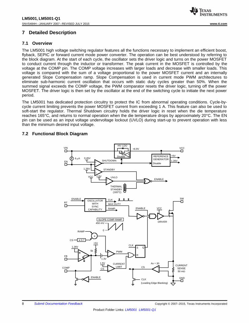
7.1 OverviewThe LM5001 high voltage switching regulator features all the functions necessary to implement an efficient boost,flyback, SEPIC or forward current mode power converter. The operation can be best understood by referring tothe block diagram. At the start of each cycle, the oscillator sets the driver logic and turns on the power MOSFETto conduct current through the inductor or transformer. The peak current in the MOSFET is controlled by thevoltage at the COMP pin. The COMP voltage increases with larger loads and decrease with smaller loads. Thisvoltage is compared with the sum of a voltage proportional to the power MOSFET current and an internallygenerated Slope Compensation ramp. Slope Compensation is used in current mode PWM architectures toeliminate sub-harmonic current oscillation that occurs with static duty cycles greater than 50%. When thesummed signal exceeds the COMP voltage, the PWM comparator resets the driver logic, turning off the powerMOSFET. The driver logic is then set by the oscillator at the end of the switching cycle to initiate the next powerperiod.
The LM5001 has dedicated protection circuitry to protect the IC from abnormal operating conditions. Cycle-by-cycle current limiting prevents the power MOSFET current from exceeding 1 A. This feature can also be used tosoft-start the regulator. Thermal Shutdown circuitry holds the driver logic in reset when the die temperaturereaches 165°C, and returns to normal operation when the die temperature drops by approximately 20°C. The ENpin can be used as an input voltage undervoltage lockout (UVLO) during start-up to prevent operation with lessthan the minimum desired input voltage.
7.2 Functional Block Diagram
8 Submit Documentation Feedback Copyright © 2007–2015, Texas Instruments Incorporated
Product Folder Links: LM5001 LM5001-Q1
RT = 13.1 x 109 x1
FSW- 83 ns
LM5001, LM5001-Q1www.ti.com SNVS484H –JANUARY 2007–REVISED JULY 2015
7.3 Feature Description
7.3.1 High-Voltage VCC RegulatorThe LM5001 VCC Low Drop Out (LDO) regulator allows the LM5001 to operate at the lowest possible inputvoltage. The VCC pin voltage is very nearly equal to the input voltage from 2.8 V up to approximately 6.9 V. Asthe input voltage continues to increase, the VCC pin voltage is regulated at the 6.9 V set-point. The total inputoperating range of the VCC LDO regulator is 3.1 V to 75 V.
The output of the VCC regulator is current limited to 20 mA. During power up, the VCC regulator supplies currentinto the required decoupling capacitor (0.47 µF or greater ceramic capacitor) at the VCC pin. When the voltage atthe VCC pin exceeds the VCC UVLO threshold of 2.8 V and the EN pin is greater than 1.26 V the PWMcontroller is enabled and switching begins. The controller remains enabled until VCC falls below 2.7 V or the ENpin falls below 1.16 V.
An auxiliary supply voltage can be applied to the VCC pin to reduce the IC power dissipation. If the auxiliaryvoltage is greater than 6.9 V, the internal regulator essentially shuts off, and internal power dissipation decreasesby the VIN voltage times the operating current. The overall converter efficiency improves if the VIN voltage ismuch higher than the auxiliary voltage. The externally applied VCC voltage should not exceed 14 V. The VCCregulator series pass MOSFET includes a body diode (Functional Block Diagram ) between VCC and VIN thatshould not be forward biased in normal operation. Therefore, the auxiliary VCC voltage should never exceed theVIN voltage.
In high voltage applications extra care should be taken to ensure the VIN pin does not exceed the absolutemaximum voltage rating of 76 V. Voltage ringing on the VIN line during line transients that exceeds the AbsoluteMaximum Ratings damages the IC. Both careful PC board layout and the use of quality bypass capacitorslocated close to the VIN and GND pins are essential.
7.3.2 OscillatorA single external resistor connected between RT and GND pins sets the LM5001 oscillator frequency. To set adesired oscillator frequency (FSW), the necessary value for the RT resistor can be calculated from:
(1)
The tolerance of the external resistor and the frequency tolerance indicated in the Electrical Characteristics mustbe taken into account when determining the worst case frequency range.
7.3.3 External SynchronizationThe LM5001 can be synchronized to the rising edge of an external clock. The external clock must have a higherfrequency than the free running oscillator frequency set by the RT resistor. The clock signal should be coupledthrough a 100 pF capacitor into the RT pin. A peak voltage level greater than 2.6 V at the RT pin is required fordetection of the sync pulse. The DC voltage across the RT resistor is internally regulated at 1.5 V. The negativeportion of the AC voltage of the synchronizing clock is clamped to this 1.5 V by an amplifier inside the LM5001with ~100 Ω output impedance. Therefore, the AC pulse superimposed on the RT resistor must have positivepulse amplitude of 1.1 V or greater to successfully synchronize the oscillator. The sync pulse width measured atthe RT pin should have a duration greater than 15 ns and less than 5% of the switching period. The sync pulserising edge initiates the internal CLK signal rising edge, which turns off the power MOSFET. The RT resistor isalways required, whether the oscillator is free running or externally synchronized. The RT resistor should belocated very close to the device and connected directly to the RT and GND pins of the LM5001.
7.3.4 Enable / StandbyThe LM5001 contains a dual level Enable circuit. When the EN pin voltage is below 450 mV, the IC is in a lowcurrent shutdown mode with the VCC LDO disabled. When the EN pin voltage is raised above the shutdownthreshold but below the 1.26 V standby threshold, the VCC LDO regulator is enabled, while the remainder of theIC is disabled. When the EN pin voltage is raised above the 1.26 V standby threshold, all functions are enabledand normal operation begins. An internal 6 µA current source pulls up the EN pin to activate the IC when the ENpin is left disconnected.
Copyright © 2007–2015, Texas Instruments Incorporated Submit Documentation Feedback 9
Product Folder Links: LM5001 LM5001-Q1

PWM
FB
5k
COMP
5VVOUT
LM5001
1
1
¸¹
ᬩ
§
1
C1
C2R2
RFEEDBACK
R1
1.3V
1.26V
FDC_POLE =
FPOLE =
FZERO =
2S x R1 x(C1 + C2)
C1 xC2
2S x R2 xC2
2S x R2 xC1 + C2
LM5001, LM5001-Q1SNVS484H –JANUARY 2007–REVISED JULY 2015 www.ti.com
Feature Description (continued)An external set-point resistor divider from VIN to GND can be used to determine the minimum operating inputrange of the regulator. The divider must be designed such that the EN pin exceeds the 1.26 V standby thresholdwhen VIN is in the desired operating range. The internal 6 µA current source should be included whendetermining the resistor values. The shutdown and standby thresholds have 100 mV hysteresis to prevent noisefrom toggling between modes. When the VIN voltage is below 3.5 VDC during start-up and the operatingtemperature is below –20°C, the EN pin should have a pull-up resistor provides 2 µA or greater current. The ENpin is internally protected by a 6 V Zener diode through a 1 kΩ resistor. The enabling voltage may exceed theZener voltage, however the Zener current should be limited to less than 4 mA.
7.3.5 Error Amplifier and PWM ComparatorAn internal high gain error amplifier generates an error signal proportional to the difference between theregulated output voltage and an internal precision reference. The output of the error amplifier is connected to theCOMP pin allowing the user to add loop compensation, typically a Type II network, as illustrated in Figure 13.This network creates a low frequency pole that rolls off the high DC gain of the amplifier, which is necessary toaccurately regulate the output voltage. FDC_POLE is the closed loop unity gain (0 dB) frequency of this pole. A zeroprovides phase boost near the closed loop unity gain frequency, and a high frequency pole attenuates switchingnoise. The PWM comparator compares the current sense signal from the current sense amplifier to the erroramplifier output voltage at the COMP pin.
Figure 13. Type II Compensator
When isolation between primary and secondary circuits is required, the Error Amplifier is usually disabled byconnecting the FB pin to GND. This allows the COMP pin to be driven directly by the collector of an opto-coupler.In isolated designs the external error amplifier is located on the secondary circuit and drives the opto-couplerLED. The compensation network is connected to the secondary side error amplifier. An example of an isolatedregulator with an opto-coupler is shown in Figure 19.
7.3.6 Current Amplifier and Slope CompensationThe LM5001 employs peak current mode control which also provides a cycle-by-cycle over current protectionfeature. An internal 50 mΩ current sense resistor measures the current in the power MOSFET source. The senseresistor voltage is amplified 30 times to provide a 1.5 V/A signal into the current limit comparator. Current limitingis initiated if the internal current limit comparator input exceeds the 1.5 V threshold, corresponding to 1 A. Whenthe current limit comparator is triggered, the SW output pin immediately switches to a high impedance state.
10 Submit Documentation Feedback Copyright © 2007–2015, Texas Instruments Incorporated
Product Folder Links: LM5001 LM5001-Q1
LM5001, LM5001-Q1www.ti.com SNVS484H –JANUARY 2007–REVISED JULY 2015
Feature Description (continued)The current sense signal is reduced to a scale factor of 1.05 V/A for the PWM comparator signal. The signal isthen summed with a 450 mV peak slope compensation ramp. The combined signal provides the PWMcomparator with a control signal that reaches 1.5 V when the MOSFET current is 1 A. For duty cycles greaterthan 50%, current mode control circuits are subject to sub-harmonic oscillation (alternating between short andlong PWM pulses every other cycle). Adding a fixed slope voltage ramp signal (slope compensation) to thecurrent sense signal prevents this oscillation. The 450 mV ramp (zero volts when the power MOSFET turns on,and 450 mV at the end of the PWM clock cycle) adds a fixed slope to the current sense ramp to preventoscillation.
To prevent erratic operation at low duty cycle, a leading edge blanking circuit attenuates the current sense signalwhen the power MOSFET is turned on. When the MOSFET is initially turned on, current spikes from the powerMOSFET drain-source and gate-source capacitances flow through the current sense resistor. These transientcurrents normally cease within 50 ns with proper selection of rectifier diodes and proper PC board layout.
7.3.7 Thermal ProtectionInternal Thermal Shutdown circuitry is provided to protect the IC in the event the maximum junction temperatureis exceeded. When the 165°C junction temperature threshold is reached, the regulator is forced into a low powerstandby state, disabling all functions except the VCC regulator. Thermal hysteresis allows the IC to cool downbefore it is re-enabled. Note that since the VCC regulator remains functional during this period, the soft-startcircuit shown in Figure 17 should be augmented if soft-start from Thermal Shutdown state is required.
7.3.8 Power MOSFETThe LM5001 switching regulator includes an N-Channel MOSFET with 440-mΩ on-resistance. The on-resistanceof the LM5001 MOSFET varies with temperature as shown in the Typical Characteristics graph. The typical totalgate charge for the MOSFET is 4.5 nC which is supplied from the VCC pin when the MOSFET is turned on.
8 Applications and Implementation
NOTEInformation in the following applications sections is not part of the TI componentspecification, and TI does not warrant its accuracy or completeness. TI’s customers areresponsible for determining suitability of components for their purposes. Customers shouldvalidate and test their design implementation to confirm system functionality.
8.1 Application InformationThis information is intended to provide guidelines for the power supply designer using the LM5001.
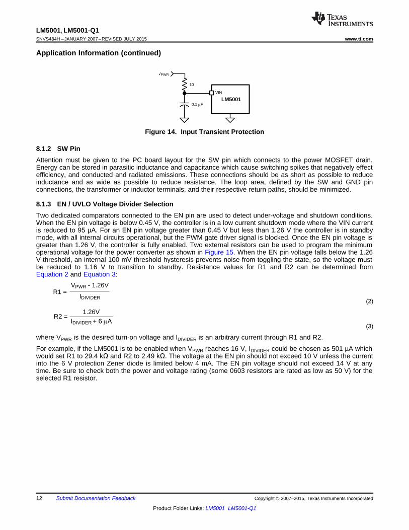
8.1.1 VINThe voltage applied to the VIN pin can vary within the range of 3.1 V to 75 V. The current into the VIN pindepends primarily on the gate charge of the power MOSFET, the switching frequency, and any external load onthe VCC pin. It is recommended the filter shown in Figure 14 be used to suppress transients which may occur atthe input supply. This is particularly important when VIN is operated close to the maximum operating rating of theLM5001.
When power is applied and the VIN voltage exceeds 2.8 V with the EN pin voltage greater than 0.45 V, the VCCregulator is enabled, supplying current into the external capacitor connected to the VCC pin. When the VINvoltage is between 2.8 V and 6.9 V, the VCC voltage is approximately equal to the VIN voltage. When thevoltage on the VCC pin exceeds 6.9 V, the VCC pin voltage is regulated at 6.9 V. In typical flyback applications,an auxiliary transformer winding is connected through a diode to the VCC pin. This winding must raise the VCCvoltage above 6.9 V to shut off the internal start-up regulator. The current requirements from this winding arerelatively small, typically less than 20 mA. If the VIN voltage is much higher than the auxiliary voltage, theauxiliary winding significantly improves conversion efficiency. It also reduces the power dissipation within theLM5001. The externally applied VCC voltage should never exceed 14 V. Also the applied VCC should neverexceed the VIN voltage to avoid reverse current through the internal VCC to VIN diode shown in the LM5001block diagram.Copyright © 2007–2015, Texas Instruments Incorporated Submit Documentation Feedback 11
Product Folder Links: LM5001 LM5001-Q1
R2 =1.26V
IDIVIDER + 6 PA
R1 =VPWR - 1.26V
IDIVIDER
10
VIN
VPWR
0.1 PFLM5001
LM5001, LM5001-Q1SNVS484H –JANUARY 2007–REVISED JULY 2015 www.ti.com
Application Information (continued)
Figure 14. Input Transient Protection
8.1.2 SW PinAttention must be given to the PC board layout for the SW pin which connects to the power MOSFET drain.Energy can be stored in parasitic inductance and capacitance which cause switching spikes that negatively effectefficiency, and conducted and radiated emissions. These connections should be as short as possible to reduceinductance and as wide as possible to reduce resistance. The loop area, defined by the SW and GND pinconnections, the transformer or inductor terminals, and their respective return paths, should be minimized.
8.1.3 EN / UVLO Voltage Divider SelectionTwo dedicated comparators connected to the EN pin are used to detect under-voltage and shutdown conditions.When the EN pin voltage is below 0.45 V, the controller is in a low current shutdown mode where the VIN currentis reduced to 95 µA. For an EN pin voltage greater than 0.45 V but less than 1.26 V the controller is in standbymode, with all internal circuits operational, but the PWM gate driver signal is blocked. Once the EN pin voltage isgreater than 1.26 V, the controller is fully enabled. Two external resistors can be used to program the minimumoperational voltage for the power converter as shown in Figure 15. When the EN pin voltage falls below the 1.26V threshold, an internal 100 mV threshold hysteresis prevents noise from toggling the state, so the voltage mustbe reduced to 1.16 V to transition to standby. Resistance values for R1 and R2 can be determined fromEquation 2 and Equation 3:
(2)
(3)
where VPWR is the desired turn-on voltage and IDIVIDER is an arbitrary current through R1 and R2.
For example, if the LM5001 is to be enabled when VPWR reaches 16 V, IDIVIDER could be chosen as 501 µA whichwould set R1 to 29.4 kΩ and R2 to 2.49 kΩ. The voltage at the EN pin should not exceed 10 V unless the currentinto the 6 V protection Zener diode is limited below 4 mA. The EN pin voltage should not exceed 14 V at anytime. Be sure to check both the power and voltage rating (some 0603 resistors are rated as low as 50 V) for theselected R1 resistor.
12 Submit Documentation Feedback Copyright © 2007–2015, Texas Instruments Incorporated
Product Folder Links: LM5001 LM5001-Q1

EN
LM5001VPWR
STANDBY
R2 OFFOFFSTANDBY
R1
1.26V
0.45V
EN
LM5001
Disable PWM Controller
R1
Disable VCC Regulator
VIN
1.26V
0.45V
6 PA
VPWR
R2
LM5001, LM5001-Q1www.ti.com SNVS484H –JANUARY 2007–REVISED JULY 2015
Application Information (continued)
Figure 15. Basic EN (UVLO) Configuration
Remote configuration of the controller’s operational modes can be accomplished with open drain device(s)connected to the EN pin as shown in Figure 16. A MOSFET or an NPN transistor connected to the EN pin canforce the regulator into the low power ‘off’ state. Adding a PN diode in the drain (or collector) provides the offsetto achieve the standby state. The advantage of standby is that the VCC LDO is not disabled and externalcircuitry powered by VCC remains functional.
Figure 16. Remote Standby and Disable Control
8.1.4 Soft-StartSoft-start (SS) can be implemented with an external capacitor connected to COMP through a diode as shown inFigure 17. The COMP discharge MOSFET conducts during Shutdown and Standby modes to keep the COMPvoltage below the PWM offset (1.3 V), which inhibits PWM pulses. The error amplifier attempts to raise theCOMP voltage after the EN pin exceeds the 1.26-V standby threshold. Because the error amplifier output canonly sink current, the internal COMP pull-up resistor (~5 kΩ) supplies the charging current to the SS capacitor.The SS capacitor causes the COMP voltage to gradually increase, until the output voltage achieves regulationand FB assumes control of the COMP and the PWM duty cycle. The SS capacitor continues charging through alarge resistance, RSS, preventing the SS circuit from interfering with the normal error amplifier function. Duringshutdown, the VCC diode discharges the SS capacitor.
Copyright © 2007–2015, Texas Instruments Incorporated Submit Documentation Feedback 13
Product Folder Links: LM5001 LM5001-Q1

PWM
VCC
FB
5k
COMP
5VVOUT
LM5001
SHUTDOWN& STANDBY
SOFT-STARTCAPACITOR
RSS
1.3V
1.26V
LM5001, LM5001-Q1SNVS484H –JANUARY 2007–REVISED JULY 2015 www.ti.com
Application Information (continued)
Figure 17. Soft-Start
8.2 Typical ApplicationsFigure 18, Figure 19, Figure 20, Figure 21, and Figure 22 present examples of a Non-Isolated Flyback, IsolatedFlyback, Boost, 24-V SEPIC and a 12-V Automotive range SEPIC converters utilizing the LM5001 switchingregulator.
8.2.1 Non-Isolated FlybackThe Non-Isolated Flyback converter (Figure 18) utilizes the internal voltage reference for the regulation setpoint.The output is 5 V at 1 A while the input voltage can vary from 16 V to 42 V. The switching frequency is set to 250kHz. An auxiliary winding on transformer (T1) provides 7.5 V to power the LM5001 when the output is inregulation. This disables the internal high voltage VCC LDO regulator and improves efficiency. The input under-voltage threshold is 13.9 V. The converter can be shut down by driving the EN input below 1.26 V with an open-collector or open-drain transistor. An external synchronizing frequency can be applied to the SYNC input. Anoptional soft-start circuit is connected to the COMP pin input. When power is applied, the soft-start capacitor (C7)is discharged and limits the voltage applied to the PWM comparator by the internal error amplifier. The internal~5 kΩ COMP pull-up resistor charges the soft-start capacitor until regulation is achieved. The VCC pull-upresistor (R7) continues to charge C7 so that the soft-start circuit will not affect the compensation network innormal operation. If the output capacitance is small, the soft-start circuit can be adjusted to limit the power-onoutput voltage overshoot. If the output capacitance is sufficiently large, no soft-start circuit is needed because theLM5001 gradually charges the output capacitor by current limiting at approximately 1 A (ILIM) until regulation isachieved.
14 Submit Documentation Feedback Copyright © 2007–2015, Texas Instruments Incorporated
Product Folder Links: LM5001 LM5001-Q1

LM
5001VIN
RTEN
GND
SW
FBCOMP
VCC
VIN = 16V ± 42V VOUT = 5V
IOUT = 1A
T1
LPRI = 160 éH8:3:2
C14.7 éF
VCC
VCC
C6100éF
D1
D2
R160.4k
R26.04k
R352.3k
LM431
R84.99k
C50.1 PF
C21 éF
C31 éF
R102.20k
R92.20k
R4249
R647
R710k
C41 éF
R5560
LM
5001VIN
RTEN
GND
SW
FBCOMP
VCC
VIN = 16V ± 42V VOUT = 5V
IOUT = 1A
T1
LPRI = 160 PH8:3:2
C14.7 PF
C31 PF
VCC
VCC
C4100 PF
D1
D2
C5220 pF
C64700 pF
R160.4k
R26.04k
R352.3k
R413.0k
R510.2k
R63.40k
EN
SYNC
C2100 pF
C710 PF
R7100k
LM5001, LM5001-Q1www.ti.com SNVS484H –JANUARY 2007–REVISED JULY 2015
Typical Applications (continued)
Figure 18. Non-Isolated Flyback
8.2.2 Isolated FlybackThe Isolated Flyback converter (Figure 19) utilizes a 2.5 V voltage reference (LM431) located on the isolatedsecondary side for the regulation setpoint. The LM5001 internal error amplifier is disabled by grounding the FBpin. The LM431 controls the current through the opto-coupler LED, which sets the COMP pin voltage. The R4and C3 network boosts the phase response of the opto-coupler to increase the loop bandwidth. The output is 5 Vat 1 A and the input voltage ranges from 16 V to 42 V. The switching frequency is set to 250 kHz.
Figure 19. Isolated Flyback
8.2.3 BoostThe Boost converter (Figure 20) utilizes the internal voltage reference for the regulation setpoint. The output is 48V at 150 mA, while the input voltage can vary from 16 V to 36 V. The switching frequency is set to 250 kHz. Theinternal VCC regulator provides 6.9 V bias power, since there isn’t a simple method for creating an auxiliaryvoltage with the boost topology. Note that the boost topology does not provide output short-circuit protectionbecause the power MOSFET cannot interrupt the path between the input and the output.
Copyright © 2007–2015, Texas Instruments Incorporated Submit Documentation Feedback 15
Product Folder Links: LM5001 LM5001-Q1

LM
5001VIN
RTEN
GND
SW
FBCOMP
VCC
VIN = 16V ± 48V VOUT = 24V
IOUT = 250 mAC14.7 éF
C21 PF
C622éF
D2
C50.015 PF
R160.4k
R26.04k
R352.3k
R411.5k
R511.5k
R6634
L1470 PH
L2470 PH
C310 PF
C4150 pF
LM
5001VIN
RTEN
GND
SW
FBCOMP
VCC
VIN = 16V ± 36V VOUT = 48V
IOUT = 150mAC14.7 éF
C21 éF
C310éF
D2
C42200 pF
R160.4k
R26.04k
R352.3k
R473.2k
R554.9k
R61.47k
L1100 PH
LM5001, LM5001-Q1SNVS484H –JANUARY 2007–REVISED JULY 2015 www.ti.com
Typical Applications (continued)
Figure 20. Boost
8.2.4 24-V SEPICThe 24-V SEPIC converter (Figure 21) utilizes the internal voltage reference for the regulation setpoint. Theoutput is 24 V at 250 mA while the input voltage can vary from 16 V to 48 V. The switching frequency is set to250 kHz. The internal VCC regulator provides 6.9 V bias power for the LM5001. An auxiliary voltage can becreated by adding a winding on L2 and a diode into the VCC pin.
Figure 21. 24-V SEPIC
8.2.5 12-V Automotive SEPICThe 12-V Automotive SEPIC converter (Figure 22) utilizes the internal bandgap voltage reference for theregulation setpoint. The output is 12 V at 50 mA while the input voltage can vary from 3.1 V to 60 V. The outputcurrent rating can be increased if the minimum VIN voltage requirement is increased. The switching frequency isset to 750 kHz. The internal VCC regulator provides 6.9 V bias power for the LM5001. The output voltage can beused as an auxiliary voltage if the nominal VIN voltage is greater than 12 V by adding a diode from the outputinto the VCC pin. In this configuration, the minimum input voltage must be greater than 12 V to prevent theinternal VCC to VIN diode from conducting. If the applied VCC voltage exceeds the minimum VIN voltage, thenan external blocking diode is required between the VIN pin and the power source to block current flow from VCCto the input supply.
16 Submit Documentation Feedback Copyright © 2007–2015, Texas Instruments Incorporated
Product Folder Links: LM5001 LM5001-Q1

LM
5001VIN
RTEN
GND
SW
FBCOMP
VCC
VIN = 3.1V ± 60V VOUT = 12V
IOUT = 50 mAC12.2 éF
C21 PF
C622 éF
D2
C50.015 PF
R115.8k
R211.5k
R311.5k
R41.33k
L1100 PH
L2100 PH
C34.7 PF
C4150 pF
NC
LM5001, LM5001-Q1www.ti.com SNVS484H –JANUARY 2007–REVISED JULY 2015
Typical Applications (continued)
Figure 22. 12-V SEPIC
Copyright © 2007–2015, Texas Instruments Incorporated Submit Documentation Feedback 17
Product Folder Links: LM5001 LM5001-Q1

LM5001, LM5001-Q1SNVS484H –JANUARY 2007–REVISED JULY 2015 www.ti.com
9 Layout
9.1 Layout GuidelinesThe LM5001 Current Sense and PWM comparators are very fast and may respond to short duration noisepulses. The components at the SW, COMP, EN and the RT pins should be as physically close as possible to theIC, thereby minimizing noise pickup on the PC board tracks.
The SW output pin of the LM5001 should have a short, wide conductor to the power path inductors, transformersand capacitors in order to minimize parasitic inductance that reduces efficiency and increases conducted andradiated noise. Ceramic decoupling capacitors are recommended between the VIN pin to the GND pin andbetween the VCC pin to the GND pin. Use short, direct connections to avoid clock jitter due to ground voltagedifferentials. Small package surface mount X7R or X5R capacitors are preferred for high frequency performanceand limited variation over temperature and applied voltage.
If an application using the LM5001 produces high junction temperatures during normal operation, multiple viasfrom the GND pin to a PC board ground plane helps conduct heat away from the IC. Judicious positioning of thePC board within the end product, along with use of any available air flow helps reduce the junction temperatures.If using forced air cooling, avoid placing the LM5001 in the airflow shadow of large components, such as inputcapacitors, inductors or transformers.
18 Submit Documentation Feedback Copyright © 2007–2015, Texas Instruments Incorporated
Product Folder Links: LM5001 LM5001-Q1

LM5001, LM5001-Q1www.ti.com SNVS484H –JANUARY 2007–REVISED JULY 2015
10 Device and Documentation Support
10.1 Related LinksThe table below lists quick access links. Categories include technical documents, support and communityresources, tools and software, and quick access to sample or buy.
Table 1. Related LinksTECHNICAL TOOLS & SUPPORT &PARTS PRODUCT FOLDER SAMPLE & BUY DOCUMENTS SOFTWARE COMMUNITY
LM5001 Click here Click here Click here Click here Click hereLM5001-Q1 Click here Click here Click here Click here Click here
10.2 TrademarksAll trademarks are the property of their respective owners.
10.3 Electrostatic Discharge CautionThese devices have limited built-in ESD protection. The leads should be shorted together or the device placed in conductive foamduring storage or handling to prevent electrostatic damage to the MOS gates.
10.4 GlossarySLYZ022 — TI Glossary.
This glossary lists and explains terms, acronyms, and definitions.
11 Mechanical, Packaging, and Orderable InformationThe following pages include mechanical packaging and orderable information. This information is the mostcurrent data available for the designated devices. This data is subject to change without notice and revision ofthis document. For browser-based versions of this data sheet, refer to the left-hand navigation.
Copyright © 2007–2015, Texas Instruments Incorporated Submit Documentation Feedback 19
Product Folder Links: LM5001 LM5001-Q1

PACKAGE OPTION ADDENDUM
www.ti.com 30-Sep-2021
Addendum-Page 1
PACKAGING INFORMATION
Orderable Device Status(1)
Package Type PackageDrawing
Pins PackageQty
Eco Plan(2)
Lead finish/Ball material
(6)
MSL Peak Temp(3)
Op Temp (°C) Device Marking(4/5)
Samples
LM5001IDQ1 ACTIVE SOIC D 8 95 RoHS & Green SN Level-1-260C-UNLIM -40 to 125 L5001IDQ1
LM5001IDRQ1 ACTIVE SOIC D 8 2500 RoHS & Green SN Level-1-260C-UNLIM -40 to 125 L5001IDQ1
LM5001MA NRND SOIC D 8 95 Non-RoHS& Green
Call TI Level-1-235C-UNLIM -40 to 125 L5001MA
LM5001MA/NOPB ACTIVE SOIC D 8 95 RoHS & Green SN Level-1-260C-UNLIM -40 to 125 L5001MA
LM5001MAX/NOPB ACTIVE SOIC D 8 2500 RoHS & Green SN Level-1-260C-UNLIM -40 to 125 L5001MA
LM5001SD/NOPB ACTIVE WSON NGT 8 1000 RoHS & Green SN Level-1-260C-UNLIM -40 to 125 LM5001
LM5001SDE/NOPB ACTIVE WSON NGT 8 250 RoHS & Green SN Level-1-260C-UNLIM -40 to 125 LM5001
LM5001SDX/NOPB ACTIVE WSON NGT 8 4500 RoHS & Green SN Level-1-260C-UNLIM -40 to 125 LM5001
(1) The marketing status values are defined as follows:ACTIVE: Product device recommended for new designs.LIFEBUY: TI has announced that the device will be discontinued, and a lifetime-buy period is in effect.NRND: Not recommended for new designs. Device is in production to support existing customers, but TI does not recommend using this part in a new design.PREVIEW: Device has been announced but is not in production. Samples may or may not be available.OBSOLETE: TI has discontinued the production of the device.
(2) RoHS: TI defines "RoHS" to mean semiconductor products that are compliant with the current EU RoHS requirements for all 10 RoHS substances, including the requirement that RoHS substancedo not exceed 0.1% by weight in homogeneous materials. Where designed to be soldered at high temperatures, "RoHS" products are suitable for use in specified lead-free processes. TI mayreference these types of products as "Pb-Free".RoHS Exempt: TI defines "RoHS Exempt" to mean products that contain lead but are compliant with EU RoHS pursuant to a specific EU RoHS exemption.Green: TI defines "Green" to mean the content of Chlorine (Cl) and Bromine (Br) based flame retardants meet JS709B low halogen requirements of <=1000ppm threshold. Antimony trioxide basedflame retardants must also meet the <=1000ppm threshold requirement.
(3) MSL, Peak Temp. - The Moisture Sensitivity Level rating according to the JEDEC industry standard classifications, and peak solder temperature.
(4) There may be additional marking, which relates to the logo, the lot trace code information, or the environmental category on the device.

PACKAGE OPTION ADDENDUM
www.ti.com 30-Sep-2021
Addendum-Page 2
(5) Multiple Device Markings will be inside parentheses. Only one Device Marking contained in parentheses and separated by a "~" will appear on a device. If a line is indented then it is a continuationof the previous line and the two combined represent the entire Device Marking for that device.
(6) Lead finish/Ball material - Orderable Devices may have multiple material finish options. Finish options are separated by a vertical ruled line. Lead finish/Ball material values may wrap to twolines if the finish value exceeds the maximum column width.
Important Information and Disclaimer:The information provided on this page represents TI's knowledge and belief as of the date that it is provided. TI bases its knowledge and belief on informationprovided by third parties, and makes no representation or warranty as to the accuracy of such information. Efforts are underway to better integrate information from third parties. TI has taken andcontinues to take reasonable steps to provide representative and accurate information but may not have conducted destructive testing or chemical analysis on incoming materials and chemicals.TI and TI suppliers consider certain information to be proprietary, and thus CAS numbers and other limited information may not be available for release.
In no event shall TI's liability arising out of such information exceed the total purchase price of the TI part(s) at issue in this document sold by TI to Customer on an annual basis.
OTHER QUALIFIED VERSIONS OF LM5001, LM5001-Q1 :
• Catalog : LM5001
• Automotive : LM5001-Q1
NOTE: Qualified Version Definitions:
• Catalog - TI's standard catalog product
• Automotive - Q100 devices qualified for high-reliability automotive applications targeting zero defects

TAPE AND REEL INFORMATION
*All dimensions are nominal
Device PackageType
PackageDrawing
Pins SPQ ReelDiameter
(mm)
ReelWidth
W1 (mm)
A0(mm)
B0(mm)
K0(mm)
P1(mm)
W(mm)
Pin1Quadrant
LM5001IDRQ1 SOIC D 8 2500 330.0 12.4 6.5 5.4 2.0 8.0 12.0 Q1
LM5001MAX/NOPB SOIC D 8 2500 330.0 12.4 6.5 5.4 2.0 8.0 12.0 Q1
LM5001SD/NOPB WSON NGT 8 1000 178.0 12.4 4.3 4.3 1.3 8.0 12.0 Q1
LM5001SDE/NOPB WSON NGT 8 250 178.0 12.4 4.3 4.3 1.3 8.0 12.0 Q1
LM5001SDX/NOPB WSON NGT 8 4500 330.0 12.4 4.3 4.3 1.3 8.0 12.0 Q1
PACKAGE MATERIALS INFORMATION
www.ti.com 5-Jan-2022
Pack Materials-Page 1

*All dimensions are nominal
Device Package Type Package Drawing Pins SPQ Length (mm) Width (mm) Height (mm)
LM5001IDRQ1 SOIC D 8 2500 367.0 367.0 35.0
LM5001MAX/NOPB SOIC D 8 2500 367.0 367.0 35.0
LM5001SD/NOPB WSON NGT 8 1000 208.0 191.0 35.0
LM5001SDE/NOPB WSON NGT 8 250 208.0 191.0 35.0
LM5001SDX/NOPB WSON NGT 8 4500 367.0 367.0 35.0
PACKAGE MATERIALS INFORMATION
www.ti.com 5-Jan-2022
Pack Materials-Page 2

TUBE
*All dimensions are nominal
Device Package Name Package Type Pins SPQ L (mm) W (mm) T (µm) B (mm)
LM5001IDQ1 D SOIC 8 95 495 8 4064 3.05
LM5001MA D SOIC 8 95 495 8 4064 3.05
LM5001MA D SOIC 8 95 495 8 4064 3.05
LM5001MA/NOPB D SOIC 8 95 495 8 4064 3.05
PACKAGE MATERIALS INFORMATION
www.ti.com 5-Jan-2022
Pack Materials-Page 3

www.ti.com
PACKAGE OUTLINE
C
8X 0.350.25
3 0.052X2.4
2.6 0.05
6X 0.8
0.8 MAX
0.050.00
8X 0.50.3
A 4.13.9
B
4.13.9
(0.2) TYP
WSON - 0.8 mm max heightNGT0008APLASTIC SMALL OUTLINE - NO LEAD
4214935/A 08/2020
PIN 1 INDEX AREA
SEATING PLANE
0.08 C
1
4 5
8
PIN 1 ID0.1 C A B0.05 C
THERMAL PADEXPOSED
SYMM
SYMM9
NOTES: 1. All linear dimensions are in millimeters. Any dimensions in parenthesis are for reference only. Dimensioning and tolerancing per ASME Y14.5M. 2. This drawing is subject to change without notice. 3. The package thermal pad must be soldered to the printed circuit board for thermal and mechanical performance.
SCALE 3.000

www.ti.com
EXAMPLE BOARD LAYOUT
0.07 MINALL AROUND
0.07 MAXALL AROUND
8X (0.3)
(3)
(3.8)
6X (0.8)
(2.6)
( 0.2) VIATYP (1.05)
(1.25)
8X (0.6)
(R0.05) TYP
WSON - 0.8 mm max heightNGT0008APLASTIC SMALL OUTLINE - NO LEAD
4214935/A 08/2020
SYMM
1
4 5
8
LAND PATTERN EXAMPLEEXPOSED METAL SHOWN
SCALE:15X
SYMM 9
NOTES: (continued) 4. This package is designed to be soldered to a thermal pad on the board. For more information, see Texas Instruments literature number SLUA271 (www.ti.com/lit/slua271).5. Vias are optional depending on application, refer to device data sheet. If any vias are implemented, refer to their locations shown on this view. It is recommended that vias under paste be filled, plugged or tented.
SOLDER MASKOPENINGSOLDER MASK
METAL UNDER
SOLDER MASKDEFINED
EXPOSEDMETAL
METALSOLDER MASKOPENING
SOLDER MASK DETAILS
NON SOLDER MASKDEFINED
(PREFERRED)
EXPOSEDMETAL

www.ti.com
EXAMPLE STENCIL DESIGN
(R0.05) TYP
(1.31)
(0.675)
8X (0.3)
8X (0.6)
(1.15)
(3.8)
(0.755)
6X (0.8)
WSON - 0.8 mm max heightNGT0008APLASTIC SMALL OUTLINE - NO LEAD
4214935/A 08/2020
NOTES: (continued) 6. Laser cutting apertures with trapezoidal walls and rounded corners may offer better paste release. IPC-7525 may have alternate design recommendations.
SOLDER PASTE EXAMPLEBASED ON 0.125 mm THICK STENCIL
EXPOSED PAD 9:
77% PRINTED SOLDER COVERAGE BY AREA UNDER PACKAGESCALE:20X
SYMM
1
4 5
8
METALTYP
SYMM 9

www.ti.com
PACKAGE OUTLINE
C
.228-.244 TYP[5.80-6.19]
.069 MAX[1.75]
6X .050[1.27]
8X .012-.020 [0.31-0.51]
2X.150[3.81]
.005-.010 TYP[0.13-0.25]
0 - 8 .004-.010[0.11-0.25]
.010[0.25]
.016-.050[0.41-1.27]
4X (0 -15 )
A
.189-.197[4.81-5.00]
NOTE 3
B .150-.157[3.81-3.98]
NOTE 4
4X (0 -15 )
(.041)[1.04]
SOIC - 1.75 mm max heightD0008ASMALL OUTLINE INTEGRATED CIRCUIT
4214825/C 02/2019
NOTES: 1. Linear dimensions are in inches [millimeters]. Dimensions in parenthesis are for reference only. Controlling dimensions are in inches. Dimensioning and tolerancing per ASME Y14.5M. 2. This drawing is subject to change without notice. 3. This dimension does not include mold flash, protrusions, or gate burrs. Mold flash, protrusions, or gate burrs shall not exceed .006 [0.15] per side. 4. This dimension does not include interlead flash.5. Reference JEDEC registration MS-012, variation AA.
18
.010 [0.25] C A B
54
PIN 1 ID AREA
SEATING PLANE
.004 [0.1] C
SEE DETAIL A
DETAIL ATYPICAL
SCALE 2.800
www.ti.com
EXAMPLE BOARD LAYOUT
.0028 MAX[0.07]ALL AROUND
.0028 MIN[0.07]ALL AROUND
(.213)[5.4]
6X (.050 )[1.27]
8X (.061 )[1.55]
8X (.024)[0.6]
(R.002 ) TYP[0.05]
SOIC - 1.75 mm max heightD0008ASMALL OUTLINE INTEGRATED CIRCUIT
4214825/C 02/2019
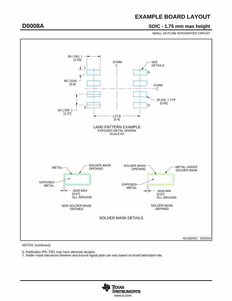
NOTES: (continued) 6. Publication IPC-7351 may have alternate designs. 7. Solder mask tolerances between and around signal pads can vary based on board fabrication site.
METALSOLDER MASKOPENING
NON SOLDER MASKDEFINED
SOLDER MASK DETAILS
EXPOSEDMETAL
OPENINGSOLDER MASK METAL UNDER
SOLDER MASK
SOLDER MASKDEFINED
EXPOSEDMETAL
LAND PATTERN EXAMPLEEXPOSED METAL SHOWN
SCALE:8X
SYMM
1
45
8
SEEDETAILS
SYMM

www.ti.com
EXAMPLE STENCIL DESIGN
8X (.061 )[1.55]
8X (.024)[0.6]
6X (.050 )[1.27]
(.213)[5.4]
(R.002 ) TYP[0.05]
SOIC - 1.75 mm max heightD0008ASMALL OUTLINE INTEGRATED CIRCUIT
4214825/C 02/2019
NOTES: (continued) 8. Laser cutting apertures with trapezoidal walls and rounded corners may offer better paste release. IPC-7525 may have alternate design recommendations. 9. Board assembly site may have different recommendations for stencil design.
SOLDER PASTE EXAMPLEBASED ON .005 INCH [0.125 MM] THICK STENCIL
SCALE:8X
SYMM
SYMM
1
45
8

IMPORTANT NOTICE AND DISCLAIMERTI PROVIDES TECHNICAL AND RELIABILITY DATA (INCLUDING DATA SHEETS), DESIGN RESOURCES (INCLUDING REFERENCE DESIGNS), APPLICATION OR OTHER DESIGN ADVICE, WEB TOOLS, SAFETY INFORMATION, AND OTHER RESOURCES “AS IS” AND WITH ALL FAULTS, AND DISCLAIMS ALL WARRANTIES, EXPRESS AND IMPLIED, INCLUDING WITHOUT LIMITATION ANY IMPLIED WARRANTIES OF MERCHANTABILITY, FITNESS FOR A PARTICULAR PURPOSE OR NON-INFRINGEMENT OF THIRD PARTY INTELLECTUAL PROPERTY RIGHTS.These resources are intended for skilled developers designing with TI products. You are solely responsible for (1) selecting the appropriate TI products for your application, (2) designing, validating and testing your application, and (3) ensuring your application meets applicable standards, and any other safety, security, regulatory or other requirements.These resources are subject to change without notice. TI grants you permission to use these resources only for development of an application that uses the TI products described in the resource. Other reproduction and display of these resources is prohibited. No license is granted to any other TI intellectual property right or to any third party intellectual property right. TI disclaims responsibility for, and you will fully indemnify TI and its representatives against, any claims, damages, costs, losses, and liabilities arising out of your use of these resources.TI’s products are provided subject to TI’s Terms of Sale or other applicable terms available either on ti.com or provided in conjunction with such TI products. TI’s provision of these resources does not expand or otherwise alter TI’s applicable warranties or warranty disclaimers for TI products.TI objects to and rejects any additional or different terms you may have proposed. IMPORTANT NOTICE
Mailing Address: Texas Instruments, Post Office Box 655303, Dallas, Texas 75265Copyright © 2022, Texas Instruments Incorporated