lm4861 1.1w audio power amplifier with shutdown mode
TRANSCRIPT
LM4861
www.ti.com SNAS095C –MAY 1997–REVISED MAY 2013
LM4861 1.1W Audio Power Amplifier with Shutdown ModeCheck for Samples: LM4861
1FEATURES DESCRIPTIONThe LM4861 is a bridge-connected audio power
2• No output coupling capacitors, bootstrapamplifier capable of delivering 1.1W of continuouscapacitors, or snubber circuits are necessaryaverage power to an 8Ω load with 1% THD+N using
• Small Outline (SOIC) packaging a 5V power supply.• Compatible with PC power supplies
Boomer audio power amplifiers were designed• Thermal shutdown protection circuitry specifically to provide high quality output power with a
minimal amount of external components using• Unity-gain stablesurface mount packaging. Since the LM4861 does• External gain configuration capabilitynot require output coupling capacitors, bootstrapcapacitors, or snubber networks, it is optimally suitedAPPLICATIONS for low-power portable systems.
• Personal computersThe LM4861 features an externally controlled, low-
• Portable consumer products power consumption shutdown mode, as well as aninternal thermal shutdown protection mechanism.• Self-powered speakers
• Toys and games The unity-gain stable LM4861 can be configured byexternal gain-setting resistors for differential gains ofup to 10 without the use of external compensationKEY SPECIFICATIONScomponents. Higher gains may be achieved with• THD+N for 1kHz at 1W continuous average suitable compensation.
output power into 8Ω 1.0% (max)• Output power at 10% THD+N at 1kHz into 8Ω
1.5 W (typ)• Shutdown Current 0.6µA (typ)
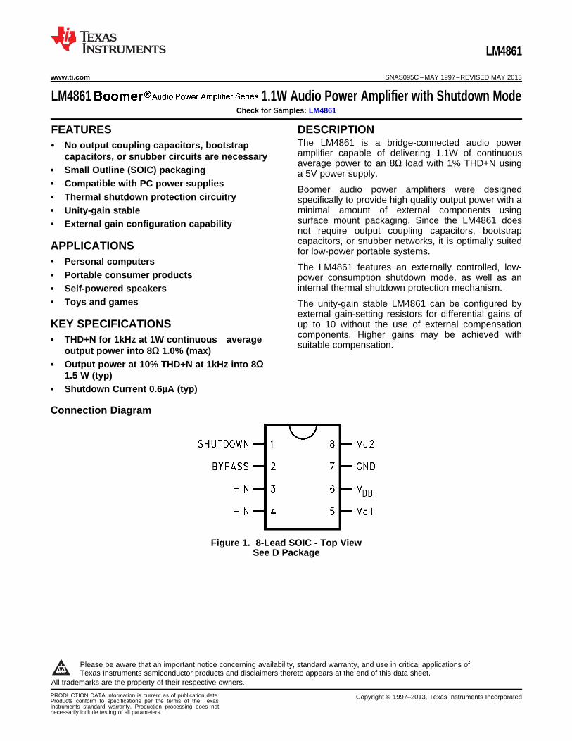
Connection Diagram
Figure 1. 8-Lead SOIC - Top ViewSee D Package
1
Please be aware that an important notice concerning availability, standard warranty, and use in critical applications ofTexas Instruments semiconductor products and disclaimers thereto appears at the end of this data sheet.
2All trademarks are the property of their respective owners.
PRODUCTION DATA information is current as of publication date. Copyright © 1997–2013, Texas Instruments IncorporatedProducts conform to specifications per the terms of the TexasInstruments standard warranty. Production processing does notnecessarily include testing of all parameters.
LM4861
SNAS095C –MAY 1997–REVISED MAY 2013 www.ti.com
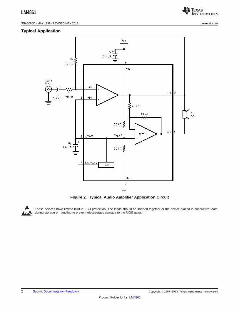
Typical Application
Figure 2. Typical Audio Amplifier Application Circuit
These devices have limited built-in ESD protection. The leads should be shorted together or the device placed in conductive foamduring storage or handling to prevent electrostatic damage to the MOS gates.
2 Submit Documentation Feedback Copyright © 1997–2013, Texas Instruments Incorporated
Product Folder Links: LM4861
LM4861
www.ti.com SNAS095C –MAY 1997–REVISED MAY 2013
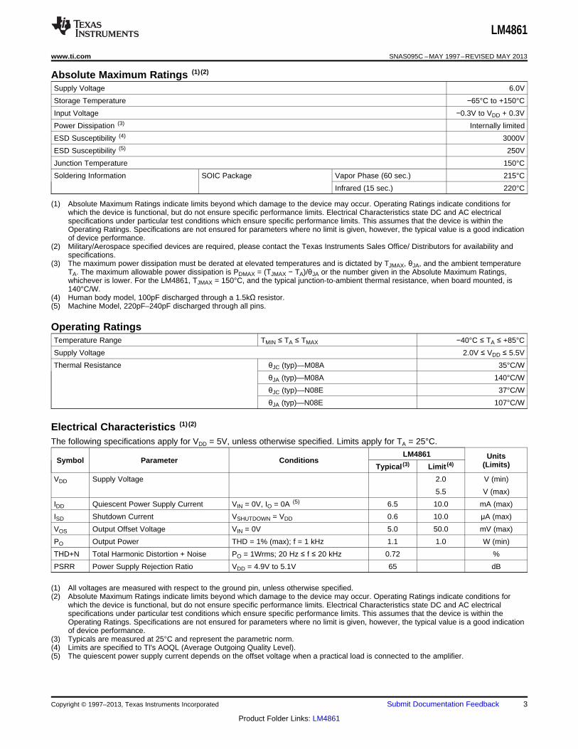
Absolute Maximum Ratings (1) (2)
Supply Voltage 6.0V
Storage Temperature −65°C to +150°C
Input Voltage −0.3V to VDD + 0.3V
Power Dissipation (3) Internally limited
ESD Susceptibility (4) 3000V
ESD Susceptibility (5) 250V
Junction Temperature 150°C
Soldering Information SOIC Package Vapor Phase (60 sec.) 215°C
Infrared (15 sec.) 220°C
(1) Absolute Maximum Ratings indicate limits beyond which damage to the device may occur. Operating Ratings indicate conditions forwhich the device is functional, but do not ensure specific performance limits. Electrical Characteristics state DC and AC electricalspecifications under particular test conditions which ensure specific performance limits. This assumes that the device is within theOperating Ratings. Specifications are not ensured for parameters where no limit is given, however, the typical value is a good indicationof device performance.
(2) Military/Aerospace specified devices are required, please contact the Texas Instruments Sales Office/ Distributors for availability andspecifications.
(3) The maximum power dissipation must be derated at elevated temperatures and is dictated by TJMAX, θJA, and the ambient temperatureTA. The maximum allowable power dissipation is PDMAX = (TJMAX − TA)/θJA or the number given in the Absolute Maximum Ratings,whichever is lower. For the LM4861, TJMAX = 150°C, and the typical junction-to-ambient thermal resistance, when board mounted, is140°C/W.
(4) Human body model, 100pF discharged through a 1.5kΩ resistor.(5) Machine Model, 220pF–240pF discharged through all pins.
Operating RatingsTemperature Range TMIN ≤ TA ≤ TMAX −40°C ≤ TA ≤ +85°C
Supply Voltage 2.0V ≤ VDD ≤ 5.5V
Thermal Resistance θJC (typ)—M08A 35°C/W
θJA (typ)—M08A 140°C/W
θJC (typ)—N08E 37°C/W
θJA (typ)—N08E 107°C/W
Electrical Characteristics (1) (2)
The following specifications apply for VDD = 5V, unless otherwise specified. Limits apply for TA = 25°C.
LM4861 UnitsSymbol Parameter Conditions (Limits)Typical (3) Limit (4)
VDD Supply Voltage 2.0 V (min)
5.5 V (max)
IDD Quiescent Power Supply Current VIN = 0V, IO = 0A (5) 6.5 10.0 mA (max)
ISD Shutdown Current VSHUTDOWN = VDD 0.6 10.0 μA (max)
VOS Output Offset Voltage VIN = 0V 5.0 50.0 mV (max)
PO Output Power THD = 1% (max); f = 1 kHz 1.1 1.0 W (min)
THD+N Total Harmonic Distortion + Noise PO = 1Wrms; 20 Hz ≤ f ≤ 20 kHz 0.72 %
PSRR Power Supply Rejection Ratio VDD = 4.9V to 5.1V 65 dB
(1) All voltages are measured with respect to the ground pin, unless otherwise specified.(2) Absolute Maximum Ratings indicate limits beyond which damage to the device may occur. Operating Ratings indicate conditions for
which the device is functional, but do not ensure specific performance limits. Electrical Characteristics state DC and AC electricalspecifications under particular test conditions which ensure specific performance limits. This assumes that the device is within theOperating Ratings. Specifications are not ensured for parameters where no limit is given, however, the typical value is a good indicationof device performance.
(3) Typicals are measured at 25°C and represent the parametric norm.(4) Limits are specified to TI's AOQL (Average Outgoing Quality Level).(5) The quiescent power supply current depends on the offset voltage when a practical load is connected to the amplifier.
Copyright © 1997–2013, Texas Instruments Incorporated Submit Documentation Feedback 3
Product Folder Links: LM4861
LM4861
SNAS095C –MAY 1997–REVISED MAY 2013 www.ti.com
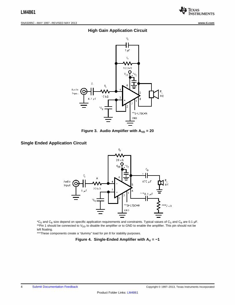
High Gain Application Circuit
Figure 3. Audio Ampiifier with AVD = 20
Single Ended Application Circuit
*CS and CB size depend on specific application requirements and constraints. Typical vaiues of CS and CB are 0.1 μF.**Pin 1 should be connected to VDD to disable the amplifier or to GND to enable the amplifier. This pin should not beleft floating.***These components create a “dummy” load for pin 8 for stability purposes.
Figure 4. Single-Ended Amplifier with AV = −1
4 Submit Documentation Feedback Copyright © 1997–2013, Texas Instruments Incorporated
Product Folder Links: LM4861
LM4861
www.ti.com SNAS095C –MAY 1997–REVISED MAY 2013
External Components Description
(Figure 2 and Figure 3)
Components Functional Description
1. Ri Inverting input resistance which sets the closed-loop gain in conjunction with Rf. This resistor also forms a high passfilter with Ci at fC = 1 / (2π Ri Ci).
2. Ci Input coupling capacitor which blocks DC voltage at the amplifier's input terminals. Also creates a high pass filter withRi at fC = 1 / (2π Ri Ci).
3. Rf Feedback resistance which sets closed-loop gain in conjunction with Ri.
4. CSApplication Supply bypass capacitor which provides power supply filtering. Refer to for proper placement and selection of supplyInformation bypass capacitor.
5. CB Bypass pin capacitor which provides half supply filtering. Refer to Application Information for proper placement andselection of bypass capacitor.
6. Cf(1) Cf in conjunction with Rf creates a low-pass filter which bandwidth limits the amplifier and prevents possible high
frequency oscillation bursts. fC = 1 / (2π Rf Cf)
(1) Optional component dependent upon specific design requirements. Refer to Application Information for more information.
Copyright © 1997–2013, Texas Instruments Incorporated Submit Documentation Feedback 5
Product Folder Links: LM4861

LM4861
SNAS095C –MAY 1997–REVISED MAY 2013 www.ti.com
Typical Performance Characteristics
THD+N THD+Nvs vs
Frequency Frequency
Figure 5. Figure 6.
THD+N THD+Nvs vs
Frequency Output Power
Figure 7. Figure 8.
THD+Nvs Output Power vs
Output Power Load Resistance
Figure 9. Figure 10.
6 Submit Documentation Feedback Copyright © 1997–2013, Texas Instruments Incorporated
Product Folder Links: LM4861

LM4861
www.ti.com SNAS095C –MAY 1997–REVISED MAY 2013
Typical Performance Characteristics (continued)Output Power vs Power Dissipation vsSupply Voltage Output Power
Figure 11. Figure 12.
Noise Floorvs Supply Current Distribution
Frequency vs Temperature
Figure 13. Figure 14.
Supply Current vsSupply Voltage Power Derating Curve
Figure 15. Figure 16.
Copyright © 1997–2013, Texas Instruments Incorporated Submit Documentation Feedback 7
Product Folder Links: LM4861
LM4861
SNAS095C –MAY 1997–REVISED MAY 2013 www.ti.com
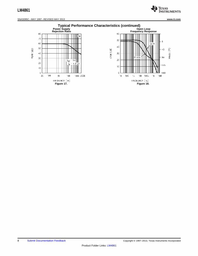
Typical Performance Characteristics (continued)Power Supply Open Loop
Rejection Ratio Frequency Response
Figure 17. Figure 18.
8 Submit Documentation Feedback Copyright © 1997–2013, Texas Instruments Incorporated
Product Folder Links: LM4861
LM4861
www.ti.com SNAS095C –MAY 1997–REVISED MAY 2013
APPLICATION INFORMATION
BRIDGE CONFIGURATION EXPLANATION
As shown in Figure 2 , the LM4861 has two operational amplifiers internally, allowing for a few different amplifierconfigurations. The first amplifier's gain is externally configurable, while the second amplifier is internally fixed ina unity-gain, inverting configuration. The closed-loop gain of the first amplifier is set by selecting the ratio of Rf toRi while the second amplifier's gain is fixed by the two internal 40kΩ resistors. Figure 2 shows that the output ofamplifier one serves as the input to amplifier two which results in both amplifiers producing signals identical inmagnitude, but out of phase 180°. Consequently, the differential gain for the IC is:
Avd = 2 * (Rf/ Ri) (1)
By driving the load differentially through outputs VO1 and VO2, an amplifier configuration commonly referred to as“bridged mode” is established. Bridged mode operation is different from the classical single-ended amplifierconfiguration where one side of its load is connected to ground.
A bridge amplifier design has a few distinct advantages over the single-ended configuration, as it providesdifferential drive to the load, thus doubling output swing for a specified supply voltage. Consequently, four timesthe output power is possible as compared to a single-ended amplifier under the same conditions. This increase inattainable output power assumes that the amplifier is not current limited or clipped. In order to choose anamplifier's closed-loop gain without causing excessive clipping which will damage high frequency transducersused in loudspeaker systems, please refer to AUDIO POWER AMPLIFIER DESIGN.
A bridge configuration, such as the one used in Boomer Audio Power Amplifiers, also creates a secondadvantage over single-ended amplifiers. Since the differential outputs, VO1 and VO2, are biased at half-supply, nonet DC voltage exists across the load. This eliminates the need for an output coupling capacitor which is requiredin a single supply, single-ended amplifier configuration. Without an output coupling capacitor in a single supply,single-ended amplifier, the half-supply bias across the load would result in both increased internal IC powerdissipation and also permanent loudspeaker damage. An output coupling capacitor forms a high pass filter withthe load requiring that a large value such as 470μF be used with an 8Ω load to preserve low frequency response.This combination does not produce a flat response down to 20Hz, but does offer a compromise between printedcircuit board size and system cost, versus low frequency response.
POWER DISSIPATION
Power dissipation is a major concern when designing a successful amplifier, whether the amplifier is bridged orsingle-ended. A direct consequence of the increased power delivered to the load by a bridge amplifier is anincrease in internal power dissipation. Equation 3 states the maximum power dissipation point for a bridgeamplifier operating at a given supply voltage and driving a specified output load.
PDMAX = 4*(VDD)2 / (2π2RL) (2)
Since the LM4861 has two operational amplifiers in one package, the maximum internal power dissipation is 4times that of a single-ended amplifier. Even with this substantial increase in power dissipation, the LM4861 doesnot require heatsinking. From Equation 3, assuming a 5V power supply and an 8Ω load, the maximum powerdissipation point is 625mW.The maximum power dissipation point obtained from Equation 3 must not be greaterthan the power dissipation that results from Equation 3:
PDMAX = (TJMAX − TA) / θJA (3)
For the LM4861 surface mount package, θJA = 140°C/W and TJMAX = 150°C. Depending on the ambienttemperature, TA, of the system surroundings, Equation 3 can be used to find the maximum internal powerdissipation supported by the IC packaging. If the result of Equation 3 is greater than that of Equation 3, theneither the supply voltage must be decreased or the load impedance increased. For the typical application of a 5Vpower supply, with an 8Ω load, the maximum ambient temperature possible without violating the maximumjunction temperature is approximately 62.5°C provided that device operation is around the maximum powerdissipation point. Power dissipation is a function of output power and thus, if typical operation is not around themaximum power dissipation point, the ambient temperature can be increased. Refer to the Typical PerformanceCharacteristics curves for power dissipation information for lower output powers.
Copyright © 1997–2013, Texas Instruments Incorporated Submit Documentation Feedback 9
Product Folder Links: LM4861
LM4861
SNAS095C –MAY 1997–REVISED MAY 2013 www.ti.com
POWER SUPPLY BYPASSING
As with any power amplifier, proper supply bypassing is critical for low noise performance and high power supplyrejection. The capacitor location on both the bypass and power supply pins should be as close to the device aspossible. As displayed in the Typical Performance Characteristics, the effect of a larger half supply bypasscapacitor is improved low frequency THD+N due to increased half-supply stability. Typical applications employ a5V regulator with 10μF and a 0.1μF bypass capacitors which aid in supply stability, but do not eliminate the needfor bypassing the supply nodes of the LM4861. The selection of bypass capacitors, especially CB, is thusdependant upon desired low frequency THD+N, system cost, and size constraints.
SHUTDOWN FUNCTION
In order to reduce power consumption while not in use, the LM4861 contains a shutdown pin to externally turn offthe amplifier's bias circuitry. The shutdown feature turns the amplifier off when a logic high is placed on theshutdown pin. Upon going into shutdown, the output is immediately disconnected from the speaker. A typicalquiescent current of 0.6μA results when the supply voltage is applied to the shutdown pin. In many applications,a microcontroller or microprocessor output is used to control the shutdown circuitry which provides a quick,smooth transition into shutdown. Another solution is to use a single-pole, single-throw switch that when closed, isconnected to ground and enables the amplifier. If the switch is open, then a soft pull-up resistor of 47kΩ willdisable the LM4861. There are no soft pull-down resistors inside the LM4861, so a definite shutdown pin voltagemust be applied externally, or the internal logic gate will be left floating which could disable the amplifierunexpectedly.
HIGHER GAIN AUDIO AMPLIFIER
The LM4861 is unity-gain stable and requires no external components besides gain-setting resistors, an inputcoupling capacitor, and proper supply bypassing in the typical application. However, if a closed-loop differentialgain of greater than 10 is required, a feedback capacitor may be needed, as shown in Figure 3, to bandwidthlimit the amplifier. This feedback capacitor creates a low pass filter that eliminates possible high frequencyoscillations. Care should be taken when calculating the −3dB frequency in that an incorrect combination of Rf andCf will cause rolloff before 20kHz. A typical combination of feedback resistor and capacitor that will not produceaudio band high frequency rolloff is Rf = 100kΩ and Cf = 5pF. These components result in a −3dB point ofapproximately 320kHz. Once the differential gain of the amplifier has been calculated, a choice of Rf will result,and Cf can then be calculated from the formula stated in External Components Description .
VOICE-BAND AUDIO AMPLIFIER
Many applications, such as telephony, only require a voice-band frequency response. Such an applicationusually requires a flat frequency response from 300Hz to 3.5kHz. By adjusting the component values of Figure 3,this common application requirement can be implemented. The combination of Ri and Ci form a highpass filterwhile Rf and Cf form a lowpass filter. Using the typical voice-band frequency range, with a passband differentialgain of approximately 100, the following values of Ri, Ci, Rf, and Cf follow from the equations stated in ExternalComponents Description .
Ri = 10kΩ, Rf = 510k ,Ci = 0.22μF, and Cf = 15pF (4)
Five times away from a −3dB point is 0.17dB down from the flatband response. With this selection ofcomponents, the resulting −3dB points, fL and fH, are 72Hz and 20kHz, respectively, resulting in a flatbandfrequency response of better than ±0.25dB with a rolloff of 6dB/octave outside of the passband. If a steeperrolloff is required, other common bandpass filtering techniques can be used to achieve higher order filters.
SINGLE-ENDED AUDIO AMPLIFIER
Although the typical application for the LM4861 is a bridged monoaural amp, it can also be used to drive a loadsingle-endedly in applications, such as PC cards, which require that one side of the load is tied to ground.Figure 4 shows a common single-ended application, where VO1 is used to drive the speaker. This output iscoupled through a 470μF capacitor, which blocks the half-supply DC bias that exists in all single-supply amplifierconfigurations. This capacitor, designated CO in Figure 4, in conjunction with RL, forms a highpass filter. The−3dB point of this high pass filter is 1/(2πRLCO), so care should be taken to make sure that the product of RL andCO is large enough to pass low frequencies to the load. When driving an 8Ω load, and if a full audio spectrumreproduction is required, CO should be at least 470μF. VO2, the output that is not used, is connected through a0.1 μF capacitor to a 2kΩ load to prevent instability. While such an instability will not affect the waveform of VO1,it is good design practice to load the second output.
10 Submit Documentation Feedback Copyright © 1997–2013, Texas Instruments Incorporated
Product Folder Links: LM4861
LM4861
www.ti.com SNAS095C –MAY 1997–REVISED MAY 2013
AUDIO POWER AMPLIFIER DESIGN
Design a 1W / 8Ω Audio Amplifier
Given:
Power Output 1 Wrms
Load Impedance 8ΩInput Level 1 Vrms
Input Impedance 20 kΩBandwidth 100 Hz–20 kHz ± 0.25 dB
A designer must first determine the needed supply rail to obtain the specified output power. By extrapolating fromFigure 11 in Typical Performance Characteristics, the supply rail can be easily found. A second way to determinethe minimum supply rail is to calculate the required Vopeak using Equation 5 and add the dropout voltage. Usingthis method, the minimum supply voltage would be (Vopeak + VOD , where VOD is typically 0.6V.
(5)
For 1W of output power into an 8Ω load, the required Vopeak is 4.0V. A minumum supply rail of 4.6V results fromadding Vopeak and Vod. But 4.6V is not a standard voltage that exists in many applications and for this reason, asupply rail of 5V is designated. Extra supply voltage creates dynamic headroom that allows the LM4861 toreproduce peaks in excess of 1Wwithout clipping the signal. At this time, the designer must make sure that thepower supply choice along with the output impedance does not violate the conditions explained in the POWERDISSIPATION.
Once the power dissipation equations have been addressed, the required differential gain can be determinedfrom Equation 6.
(6)Rf/Ri = AVD / 2 (7)
From Equation 6, the minimum Avd is 2.83: Avd = 3
Since the desired input impedance was 20kΩ, and with a Avd of 3, a ratio of 1:1.5 of Rf to Ri results in anallocation of Ri = 20kΩ, Rf = 30kΩ. The final design step is to address the bandwidth requirements which mustbe stated as a pair of −3dB frequency points. Five times away from a −3db point is 0.17dB down from passbandresponse which is better than the required ±0.25dB specified. This fact results in a low and high frequency poleof 20Hz and 100kHz respectively. As stated in External Components Description , Ri in conjunction with Ci createa highpass filter.
Ci ≥ 1 / (2π*20kΩ*20Hz) = 0.397μF; use 0.39μF. (8)
The high frequency pole is determined by the product of the desired high frequency pole, fH, and the differentialgain, Avd. With a Avd = 2 and fH = 100kHz, the resulting GBWP = 100kHz which is much smaller than the LM4861GBWP of 4MHz. This figure displays that if a designer has a need to design an amplifier with a higher differentialgain, the LM4861 can still be used without running into bandwidth problems.
Copyright © 1997–2013, Texas Instruments Incorporated Submit Documentation Feedback 11
Product Folder Links: LM4861

LM4861
SNAS095C –MAY 1997–REVISED MAY 2013 www.ti.com
LM4861 MDA MWA1.1W Audio Power Amplifier with Shutdown Mode
Figure 19. Die Layout (B - Step)
Table 1. DIE/WAFER CHARACTERISTICS
Fabrication Attributes General Die Information
Physical Die Identification LM4861B Bond Pad Opening Size (min) 83µm x 83µm
Die Step B Bond Pad Metalization ALUMINUM
Physical Attributes Passivation VOM NITRIDE
Wafer Diameter 150mm Back Side Metal BARE BACK
Dise Size (Drawn) 1372µm x 2032µm Back Side Connection GND54.0mils x 80.0mils
Thickness 406µm Nominal
Min Pitch 108µm Nominal
Special Assembly Requirements:
Note: Actual die size is rounded to the nearest micron.
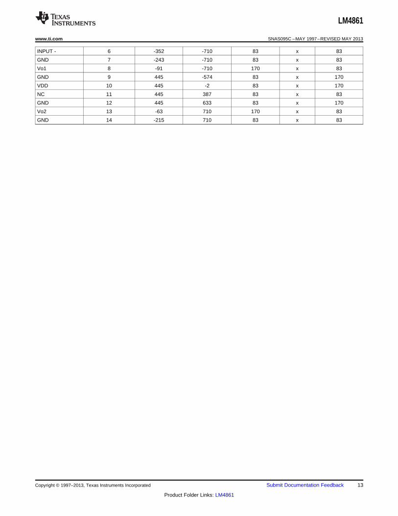
Die Bond Pad Coordinate Locations (B - Step)
(Referenced to die center, coordinates in µm) NC = No Connection, N.U. = Not Used
X/Y COORDINATES PAD SIZESIGNAL NAME PAD# NUMBER
X Y X Y
SHUTDOWN 1 -425 710 83 x 83
BYPASS 2 -445 499 83 x 83
NC 3 -445 -34 83 x 170
NC 4 -445 -383 83 x 83
INPUT + 5 -445 -492 83 x 83
12 Submit Documentation Feedback Copyright © 1997–2013, Texas Instruments Incorporated
Product Folder Links: LM4861
LM4861
www.ti.com SNAS095C –MAY 1997–REVISED MAY 2013
INPUT - 6 -352 -710 83 x 83
GND 7 -243 -710 83 x 83
Vo1 8 -91 -710 170 x 83
GND 9 445 -574 83 x 170
VDD 10 445 -2 83 x 170
NC 11 445 387 83 x 83
GND 12 445 633 83 x 170
Vo2 13 -63 710 170 x 83
GND 14 -215 710 83 x 83
Copyright © 1997–2013, Texas Instruments Incorporated Submit Documentation Feedback 13
Product Folder Links: LM4861
LM4861
SNAS095C –MAY 1997–REVISED MAY 2013 www.ti.com
REVISION HISTORY
Changes from Revision B (May 2013) to Revision C Page
• Changed layout of National Data Sheet to TI format .......................................................................................................... 13
14 Submit Documentation Feedback Copyright © 1997–2013, Texas Instruments Incorporated
Product Folder Links: LM4861
PACKAGE OPTION ADDENDUM
www.ti.com 30-Sep-2021
Addendum-Page 1
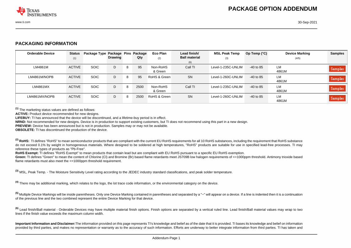
PACKAGING INFORMATION
Orderable Device Status(1)
Package Type PackageDrawing
Pins PackageQty
Eco Plan(2)
Lead finish/Ball material
(6)
MSL Peak Temp(3)
Op Temp (°C) Device Marking(4/5)
Samples
LM4861M ACTIVE SOIC D 8 95 Non-RoHS& Green
Call TI Level-1-235C-UNLIM -40 to 85 LM4861M
LM4861M/NOPB ACTIVE SOIC D 8 95 RoHS & Green SN Level-1-260C-UNLIM -40 to 85 LM4861M
LM4861MX ACTIVE SOIC D 8 2500 Non-RoHS& Green
Call TI Level-1-235C-UNLIM -40 to 85 LM4861M
LM4861MX/NOPB ACTIVE SOIC D 8 2500 RoHS & Green SN Level-1-260C-UNLIM -40 to 85 LM4861M
(1) The marketing status values are defined as follows:ACTIVE: Product device recommended for new designs.LIFEBUY: TI has announced that the device will be discontinued, and a lifetime-buy period is in effect.NRND: Not recommended for new designs. Device is in production to support existing customers, but TI does not recommend using this part in a new design.PREVIEW: Device has been announced but is not in production. Samples may or may not be available.OBSOLETE: TI has discontinued the production of the device.
(2) RoHS: TI defines "RoHS" to mean semiconductor products that are compliant with the current EU RoHS requirements for all 10 RoHS substances, including the requirement that RoHS substancedo not exceed 0.1% by weight in homogeneous materials. Where designed to be soldered at high temperatures, "RoHS" products are suitable for use in specified lead-free processes. TI mayreference these types of products as "Pb-Free".RoHS Exempt: TI defines "RoHS Exempt" to mean products that contain lead but are compliant with EU RoHS pursuant to a specific EU RoHS exemption.Green: TI defines "Green" to mean the content of Chlorine (Cl) and Bromine (Br) based flame retardants meet JS709B low halogen requirements of <=1000ppm threshold. Antimony trioxide basedflame retardants must also meet the <=1000ppm threshold requirement.
(3) MSL, Peak Temp. - The Moisture Sensitivity Level rating according to the JEDEC industry standard classifications, and peak solder temperature.
(4) There may be additional marking, which relates to the logo, the lot trace code information, or the environmental category on the device.
(5) Multiple Device Markings will be inside parentheses. Only one Device Marking contained in parentheses and separated by a "~" will appear on a device. If a line is indented then it is a continuationof the previous line and the two combined represent the entire Device Marking for that device.
(6) Lead finish/Ball material - Orderable Devices may have multiple material finish options. Finish options are separated by a vertical ruled line. Lead finish/Ball material values may wrap to twolines if the finish value exceeds the maximum column width.
Important Information and Disclaimer:The information provided on this page represents TI's knowledge and belief as of the date that it is provided. TI bases its knowledge and belief on informationprovided by third parties, and makes no representation or warranty as to the accuracy of such information. Efforts are underway to better integrate information from third parties. TI has taken and

PACKAGE OPTION ADDENDUM
www.ti.com 30-Sep-2021
Addendum-Page 2
continues to take reasonable steps to provide representative and accurate information but may not have conducted destructive testing or chemical analysis on incoming materials and chemicals.TI and TI suppliers consider certain information to be proprietary, and thus CAS numbers and other limited information may not be available for release.
In no event shall TI's liability arising out of such information exceed the total purchase price of the TI part(s) at issue in this document sold by TI to Customer on an annual basis.

TAPE AND REEL INFORMATION
*All dimensions are nominal
Device PackageType
PackageDrawing
Pins SPQ ReelDiameter
(mm)
ReelWidth
W1 (mm)
A0(mm)
B0(mm)
K0(mm)
P1(mm)
W(mm)
Pin1Quadrant
LM4861MX SOIC D 8 2500 330.0 12.4 6.5 5.4 2.0 8.0 12.0 Q1
LM4861MX/NOPB SOIC D 8 2500 330.0 12.4 6.5 5.4 2.0 8.0 12.0 Q1
PACKAGE MATERIALS INFORMATION
www.ti.com 8-May-2013
Pack Materials-Page 1
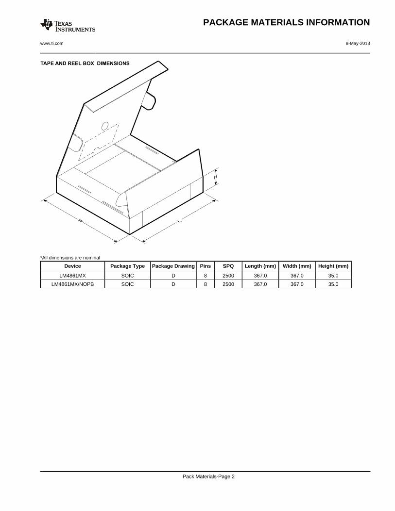
*All dimensions are nominal
Device Package Type Package Drawing Pins SPQ Length (mm) Width (mm) Height (mm)
LM4861MX SOIC D 8 2500 367.0 367.0 35.0
LM4861MX/NOPB SOIC D 8 2500 367.0 367.0 35.0
PACKAGE MATERIALS INFORMATION
www.ti.com 8-May-2013
Pack Materials-Page 2
www.ti.com
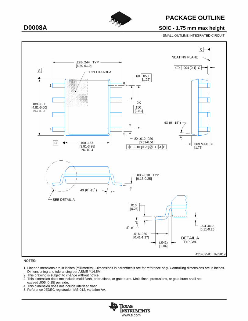
PACKAGE OUTLINE
C
.228-.244 TYP[5.80-6.19]
.069 MAX[1.75]
6X .050[1.27]
8X .012-.020 [0.31-0.51]
2X.150[3.81]
.005-.010 TYP[0.13-0.25]
0 - 8 .004-.010[0.11-0.25]
.010[0.25]
.016-.050[0.41-1.27]
4X (0 -15 )
A
.189-.197[4.81-5.00]
NOTE 3
B .150-.157[3.81-3.98]
NOTE 4
4X (0 -15 )
(.041)[1.04]
SOIC - 1.75 mm max heightD0008ASMALL OUTLINE INTEGRATED CIRCUIT
4214825/C 02/2019
NOTES: 1. Linear dimensions are in inches [millimeters]. Dimensions in parenthesis are for reference only. Controlling dimensions are in inches. Dimensioning and tolerancing per ASME Y14.5M. 2. This drawing is subject to change without notice. 3. This dimension does not include mold flash, protrusions, or gate burrs. Mold flash, protrusions, or gate burrs shall not exceed .006 [0.15] per side. 4. This dimension does not include interlead flash.5. Reference JEDEC registration MS-012, variation AA.
18
.010 [0.25] C A B
54
PIN 1 ID AREA
SEATING PLANE
.004 [0.1] C
SEE DETAIL A
DETAIL ATYPICAL
SCALE 2.800
www.ti.com
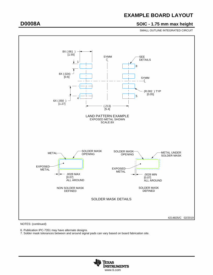
EXAMPLE BOARD LAYOUT
.0028 MAX[0.07]ALL AROUND
.0028 MIN[0.07]ALL AROUND
(.213)[5.4]
6X (.050 )[1.27]
8X (.061 )[1.55]
8X (.024)[0.6]
(R.002 ) TYP[0.05]
SOIC - 1.75 mm max heightD0008ASMALL OUTLINE INTEGRATED CIRCUIT
4214825/C 02/2019
NOTES: (continued) 6. Publication IPC-7351 may have alternate designs. 7. Solder mask tolerances between and around signal pads can vary based on board fabrication site.
METALSOLDER MASKOPENING
NON SOLDER MASKDEFINED
SOLDER MASK DETAILS
EXPOSEDMETAL
OPENINGSOLDER MASK METAL UNDER
SOLDER MASK
SOLDER MASKDEFINED
EXPOSEDMETAL
LAND PATTERN EXAMPLEEXPOSED METAL SHOWN
SCALE:8X
SYMM
1
45
8
SEEDETAILS
SYMM
www.ti.com
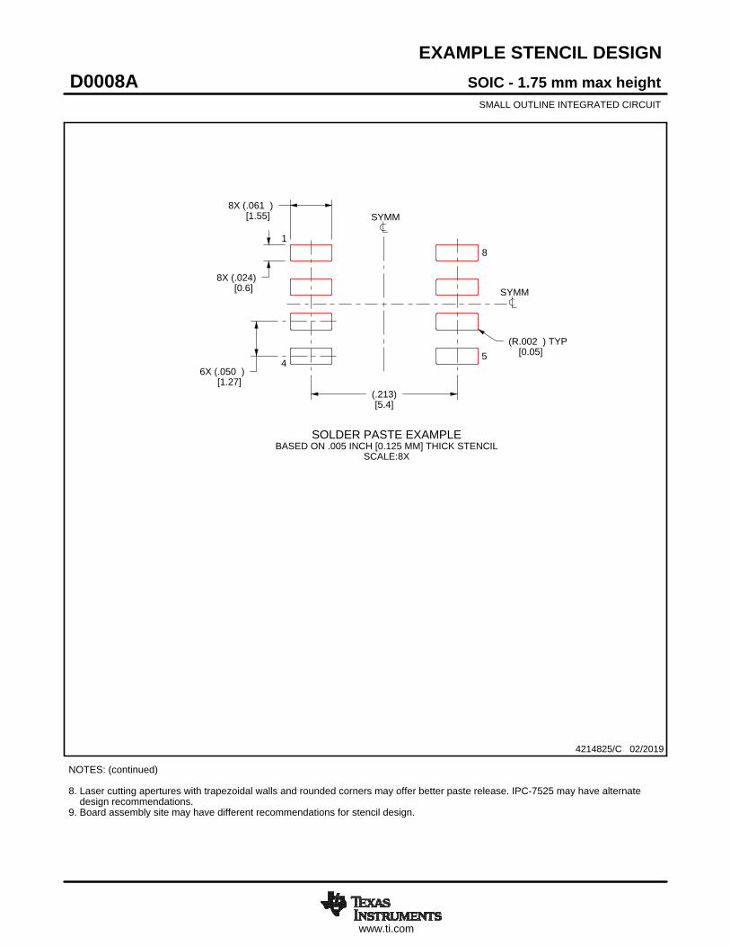
EXAMPLE STENCIL DESIGN
8X (.061 )[1.55]
8X (.024)[0.6]
6X (.050 )[1.27]
(.213)[5.4]
(R.002 ) TYP[0.05]
SOIC - 1.75 mm max heightD0008ASMALL OUTLINE INTEGRATED CIRCUIT
4214825/C 02/2019
NOTES: (continued) 8. Laser cutting apertures with trapezoidal walls and rounded corners may offer better paste release. IPC-7525 may have alternate design recommendations. 9. Board assembly site may have different recommendations for stencil design.
SOLDER PASTE EXAMPLEBASED ON .005 INCH [0.125 MM] THICK STENCIL
SCALE:8X
SYMM
SYMM
1
45
8

IMPORTANT NOTICE AND DISCLAIMERTI PROVIDES TECHNICAL AND RELIABILITY DATA (INCLUDING DATASHEETS), DESIGN RESOURCES (INCLUDING REFERENCEDESIGNS), APPLICATION OR OTHER DESIGN ADVICE, WEB TOOLS, SAFETY INFORMATION, AND OTHER RESOURCES “AS IS”AND WITH ALL FAULTS, AND DISCLAIMS ALL WARRANTIES, EXPRESS AND IMPLIED, INCLUDING WITHOUT LIMITATION ANYIMPLIED WARRANTIES OF MERCHANTABILITY, FITNESS FOR A PARTICULAR PURPOSE OR NON-INFRINGEMENT OF THIRDPARTY INTELLECTUAL PROPERTY RIGHTS.These resources are intended for skilled developers designing with TI products. You are solely responsible for (1) selecting the appropriateTI products for your application, (2) designing, validating and testing your application, and (3) ensuring your application meets applicablestandards, and any other safety, security, or other requirements. These resources are subject to change without notice. TI grants youpermission to use these resources only for development of an application that uses the TI products described in the resource. Otherreproduction and display of these resources is prohibited. No license is granted to any other TI intellectual property right or to any third partyintellectual property right. TI disclaims responsibility for, and you will fully indemnify TI and its representatives against, any claims, damages,costs, losses, and liabilities arising out of your use of these resources.TI’s products are provided subject to TI’s Terms of Sale (https:www.ti.com/legal/termsofsale.html) or other applicable terms available eitheron ti.com or provided in conjunction with such TI products. TI’s provision of these resources does not expand or otherwise alter TI’sapplicable warranties or warranty disclaimers for TI products.IMPORTANT NOTICE
Mailing Address: Texas Instruments, Post Office Box 655303, Dallas, Texas 75265Copyright © 2021, Texas Instruments Incorporated