lm3553 1.2a dual flash led driver system with i2c ... · pdf filean-1780lm3553 1.2a dual flash...
TRANSCRIPT
Application ReportSNVA319B–February 2008–Revised April 2013
AN-1780 LM3553 1.2A Dual Flash LED Driver System withI2C Compatible Interface
.....................................................................................................................................................
ABSTRACT
This application note describes how to operate the LM3553 Evaluation Module.
Contents1 Typical Application Drawing ............................................................................................... 22 Bill of Materials .............................................................................................................. 23 Schematic .................................................................................................................... 34 LM3553 Evaluation Board Layout ........................................................................................ 35 Board Operation ............................................................................................................. 4
5.1 Basic Connections ................................................................................................. 45.2 External Control Interface Connection .......................................................................... 55.3 Operation Description ............................................................................................. 5
6 Software Interface Information ........................................................................................... 11
List of Figures
1 Top Layer .................................................................................................................... 3
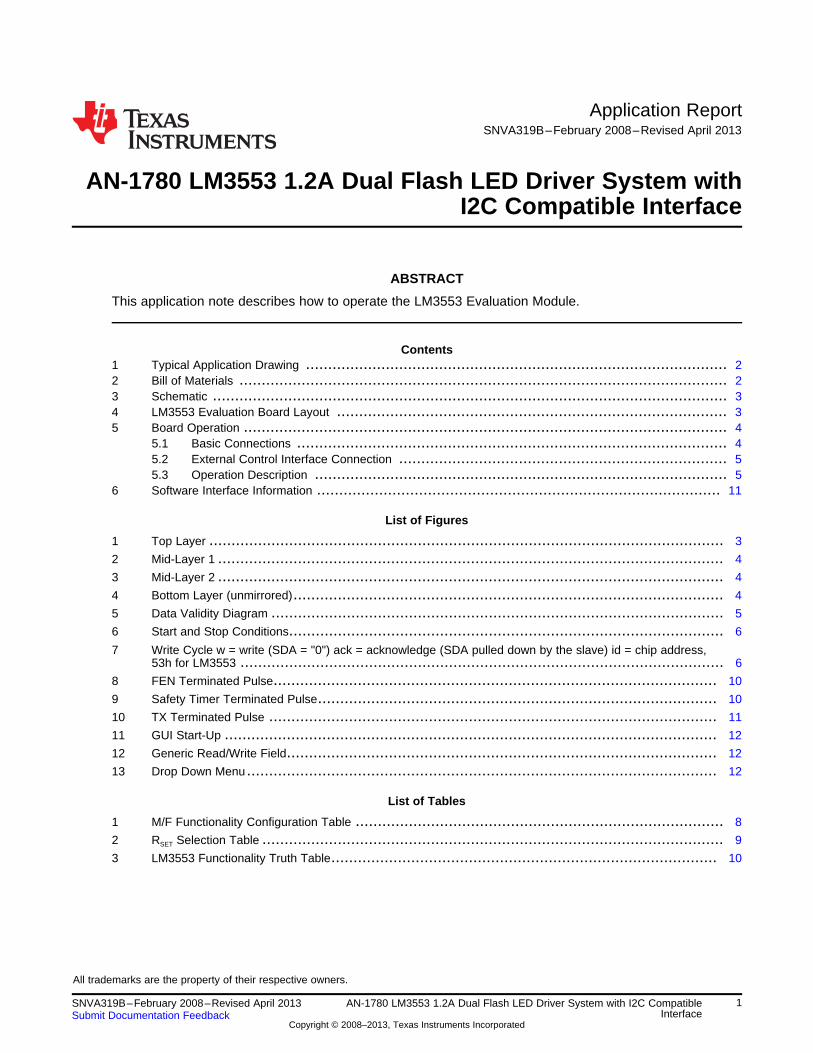
2 Mid-Layer 1 .................................................................................................................. 4
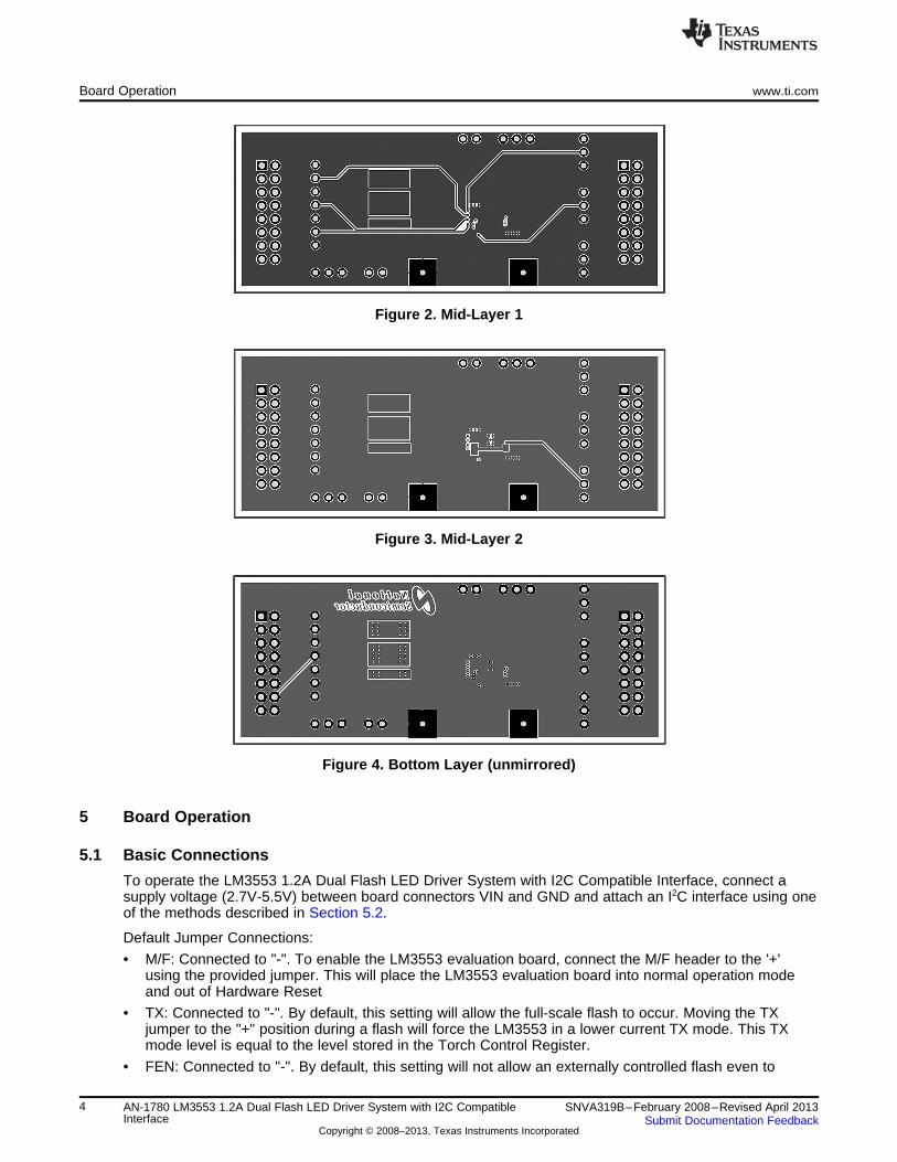
3 Mid-Layer 2 .................................................................................................................. 4
4 Bottom Layer (unmirrored)................................................................................................. 4
5 Data Validity Diagram ...................................................................................................... 5
6 Start and Stop Conditions.................................................................................................. 6
7 Write Cycle w = write (SDA = "0") ack = acknowledge (SDA pulled down by the slave) id = chip address,53h for LM3553 ............................................................................................................. 6
8 FEN Terminated Pulse.................................................................................................... 10
9 Safety Timer Terminated Pulse.......................................................................................... 10
10 TX Terminated Pulse ..................................................................................................... 11
11 GUI Start-Up ............................................................................................................... 12
12 Generic Read/Write Field................................................................................................. 12
13 Drop Down Menu .......................................................................................................... 12
List of Tables
1 M/F Functionality Configuration Table ................................................................................... 8
2 RSET Selection Table ........................................................................................................ 9
3 LM3553 Functionality Truth Table....................................................................................... 10
All trademarks are the property of their respective owners.
1SNVA319B–February 2008–Revised April 2013 AN-1780 LM3553 1.2A Dual Flash LED Driver System with I2C CompatibleInterfaceSubmit Documentation Feedback
Copyright © 2008–2013, Texas Instruments Incorporated

Typical Application Drawing www.ti.com
1 Typical Application Drawing
2 Bill of Materials
Component Symbol Value Package Manufacturer Part #
LM3553 -- SDF12A Texas Instruments LM3553SDXLLP12
LM3553 Evaluation -- -- Texas Instruments 551600092-001 RevABoard
LED1,LED2 White LED -- Philips Lumiled LXCL-PWF3
CIN 10µF, 6.3V 0603 Murata GRM188R60J106ME47D
COUT 4.7µF, 25V 0805 Murata GRM21BR61E475KA12L
L1 2.2µH 3mm x 3mm x 1.2mm Toko FDSE0312-2R2M
RSET 33kΩ 0402 Vishay Dale CRCW040233K0FKED
D1 1.5A, 30V ROHM RB070M-30
RSDA, RSCL, RFEN, 10kΩ 0402 Vishay Dale CRCW040210K0JNEDRMF, RTX
2 AN-1780 LM3553 1.2A Dual Flash LED Driver System with I2C Compatible SNVA319B–February 2008–Revised April 2013Interface Submit Documentation Feedback
Copyright © 2008–2013, Texas Instruments Incorporated

www.ti.com Schematic
3 Schematic
4 LM3553 Evaluation Board Layout
Figure 1. Top Layer
3SNVA319B–February 2008–Revised April 2013 AN-1780 LM3553 1.2A Dual Flash LED Driver System with I2C CompatibleInterfaceSubmit Documentation Feedback
Copyright © 2008–2013, Texas Instruments Incorporated
Board Operation www.ti.com
Figure 2. Mid-Layer 1
Figure 3. Mid-Layer 2
Figure 4. Bottom Layer (unmirrored)
5 Board Operation
5.1 Basic Connections
To operate the LM3553 1.2A Dual Flash LED Driver System with I2C Compatible Interface, connect asupply voltage (2.7V-5.5V) between board connectors VIN and GND and attach an I2C interface using oneof the methods described in Section 5.2.
Default Jumper Connections:
• M/F: Connected to "-". To enable the LM3553 evaluation board, connect the M/F header to the '+'using the provided jumper. This will place the LM3553 evaluation board into normal operation modeand out of Hardware Reset
• TX: Connected to "-". By default, this setting will allow the full-scale flash to occur. Moving the TXjumper to the "+" position during a flash will force the LM3553 in a lower current TX mode. This TXmode level is equal to the level stored in the Torch Control Register.
• FEN: Connected to "-". By default, this setting will not allow an externally controlled flash even to
4 AN-1780 LM3553 1.2A Dual Flash LED Driver System with I2C Compatible SNVA319B–February 2008–Revised April 2013Interface Submit Documentation Feedback
Copyright © 2008–2013, Texas Instruments Incorporated

www.ti.com Board Operation
occur. Moving the FEN jumper to the "+" position will start a flash event. The flash event will remainactive until the FEN pin is driven back to the "-" position or the internal timeout time lapses, which everoccurs first.
With the default jumper connections made, the board will be ready to operate once an input voltage andan I2C interface generator (external or USB docking board) are connected.
NOTE: For the evaluation board to work properly, the OVP bit in the Multi-Function/Options Registermust be set to a 1 (18.9V OVP). If this bit is not enabled, the part will not boost to therequired voltage and performance will be degraded.
5.2 External Control Interface Connection
The LM3553 Evaluation Board provides two ways to connect an I2C compatible interface to the LM3553IC. The first method to connect the interface is through a set of connectors on the bottom of the evaluationboard that allow the board to plug into the USB interface board directly. The second method of interfaceconnection is through a header strip located on the left hand side of the evaluation board. There are pinsavailable to connect VIO (contoller reference voltage), SCL (Interface Clock Line), and SDA (InterfaceData Line) each separated by a ground pin. The evaluation board has two external pull-ups that connectboth SCL and SDA to VIO to compliment the open drain inputs found on the LM3553. Section 5.3describes the internal registers and I2C compatible interface in greater detail.
5.3 Operation Description
5.3.1 I2C Compatible Interface
5.3.1.1 Data Validity
The data on SDA line must be stable during the HIGH period of the clock signal (SCL). In other words, thestate of the data line can only be changed when CLK is LOW.
Figure 5. Data Validity Diagram
A pull-up resistor between VIO and SDA must be greater than [(VIO-VOL) / 3.7mA] to meet the VOL
requirement on SDA. Using a larger pull-up resistor results in lower switching current with slower edges,while using a smaller pull-up results in higher switching currents with faster edges.
5.3.1.2 Start and Stop Conditions
START and STOP conditions classify the beginning and the end of the I2C session. A START condition isdefined as SDA signal transitioning from HIGH to LOW while SCL line is HIGH. A STOP condition isdefined as the SDA transitioning from LOW to HIGH while SCL is HIGH. The I2C master always generatesSTART and STOP conditions. The I2C bus is considered to be busy after a START condition and freeafter a STOP condition. During data transmission, the I2C master can generate repeated STARTconditions. First START and repeated START conditions are equivalent, function-wise. The data on SDAline must be stable during the HIGH period of the clock signal (SCL). In other words, the state of the dataline can only be changed when CLK is LOW.
5SNVA319B–February 2008–Revised April 2013 AN-1780 LM3553 1.2A Dual Flash LED Driver System with I2C CompatibleInterfaceSubmit Documentation Feedback
Copyright © 2008–2013, Texas Instruments Incorporated

Board Operation www.ti.com
Figure 6. Start and Stop Conditions
5.3.1.3 Transferring Data
Every byte put on the SDA line must be eight bits long, with the most significant bit (MSB) beingtransferred first. Each byte of data has to be followed by an acknowledge bit. The acknowledge relatedclock pulse is generated by the master. The master releases the SDA line (HIGH) during the acknowledgeclock pulse. The LM3553 pulls down the SDA line during the 9th clock pulse, signifying an acknowledge.The LM3553 generates an acknowledge after each byte has been received.
After the START condition, the I2C master sends a chip address. This address is seven bits long followedby an eighth bit which is a data direction bit (R/W). The LM3553 address is 53h. For the eighth bit, a “0”indicates a WRITE and a “1” indicates a READ. The second byte selects the register to which the data willbe written. The third byte contains data to write to the selected register.
Figure 7. Write Cyclew = write (SDA = "0")
ack = acknowledge (SDA pulled down by the slave)id = chip address, 53h for LM3553
5.3.1.4 I2C Compatible Chip Address
The chip address for LM3553 is 1010011, or 53hex.
6 AN-1780 LM3553 1.2A Dual Flash LED Driver System with I2C Compatible SNVA319B–February 2008–Revised April 2013Interface Submit Documentation Feedback
Copyright © 2008–2013, Texas Instruments Incorporated

www.ti.com Board Operation
5.3.1.5 Internal Registers of LM3553
Register Internal Hex Address Power On Value
General Purpose Register 0x10 0001 1000
Multi-Function Pin Control Register 0x20 1110 0000
Current Step Time Register 0x50 1111 1100
Torch Current Control Register 0xA0 1000 0000
Flash Current Control Register 0xB0 1000 0000
Flash Duration Control Register 0xC0 1111 0000
5.3.1.5.1 General-Purpose Register
EN0-EN1: Set Flash LED mode
Indicator Mode sets ILED = 20mA. In this mode, D1 is enabled and D2 is disabled.
VM: Enables Voltage Mode. Current sinks D1 and D2 are turned off and the LM3553 will operate in aregulated voltage boost mode. Setting the VM bit to a '1' does not override the EN0 and EN1 bits stored inthe general purpose register. The default setting is '0'. If the LM3553 is in Voltage Mode and an indicator,torch or flash command is issued, the LM3553 will turn on the D1 and D2 current sources and beginregulating the output voltage to a value equal to VFB (350mV or 450mV) + VLED.
VM EN1 EN0 Function
0 0 0 Shutdown
0 0 1 Indicator Mode
0 1 0 Torch Mode
0 1 1 Flash Mode
1 0 0 Voltage Mode
1 0 1 Indicator Mode
1 1 0 Torch Mode
1 1 1 Flash Mode
VFB: Selects the regulation voltage for the LM3553. Setting this VFB bit to a '0' sets the regulation voltageto 450mV while setting the VFB bit to a '1' sets the regulation voltage to 350mV. Setting the VFB bit to a'1' during torch mode and/or lower current flash modes (ILED < 1A) will help improve the LED efficiency ofthe LM3553.
5.3.1.5.2 M/F Pin Control Register
RESET: Enables M/F as hardware RESET. '0' = Hardware RESET, .'1' = GPIO or current sink dependingon the MODE bit. Default = '0'
MODE: Sets M/F mode. Default for M0DE = '0'. '0' = GPI, and'1' = GPO
7SNVA319B–February 2008–Revised April 2013 AN-1780 LM3553 1.2A Dual Flash LED Driver System with I2C CompatibleInterfaceSubmit Documentation Feedback
Copyright © 2008–2013, Texas Instruments Incorporated

Board Operation www.ti.com
NOTE: When M/F is configured as an input, data is transfered from GPI to DATA whenever an I2Cwrite command is issued to the LM3553. When configuring M/F as a GPO, the first writeneeds to take the LM3553 out of RESET mode and a second write can then set the pin tothe GPO.
DATA: GPIO Data. When the M/F is configured as an output (GPO), DATA sets the GPO level. Example:DATA = '1', M/F is set high or logic '1'. When the M/F pin is configured as an input (GPI), DATA stores theGPI level. Example: M/F = '1', DATA will be set to a '1'. Default for DATA = '0'.
OVP: Enables high-voltage OVP (OVP Bit ='1') or low-voltage OVP (OVP Bit ='0'). Default = low-voltagemode '0'
OCL: SW Pin Current Limit Selector Bit: If OCL = '0', the inductor current limit is 2.5A typ. If OCL = '1', theinductor current limit is 1.7A typ.
Table 1. M/F Functionality Configuration Table
RESET MODE M/F Function
0 X RESET
1 0 GPI
1 1 GPO
5.3.1.5.3 Current Step Time Register
ST1-ST0: Sets current level stepping time for D1 and D2 during the beginning and end of the flash ortorch current waveform. '00' = 25µs, '01' = 50µs, '10' = 100µs, '11' = 200µs.
The current ramp-up/ramp-down times can be approximated by the following equation:
TRAMPUP/RAMPDOWN = (NFLASH - NSTART + 1) × tSTEP where N is equal to the decimal value of the brightness level(0 ≤ NFLASH ≤ 127 and 0 ≤ NSTART ≤ 31). NSTART = NTORCH if Torch is enabled before going into a flash. Ifgoing straight into a flash from an off-state, NSTART = 0
5.3.1.5.4 Torch Current Control Register
TC6-TC0: Sets Torch current level for D1 and D2. xxx1 1111 = Full-scale
5.3.1.5.5 Flash Current Control Register
FC6-FC0: Sets Flash current level for D1 and D2. x111 1111 = Full-scale
8 AN-1780 LM3553 1.2A Dual Flash LED Driver System with I2C Compatible SNVA319B–February 2008–Revised April 2013Interface Submit Documentation Feedback
Copyright © 2008–2013, Texas Instruments Incorporated
www.ti.com Board Operation
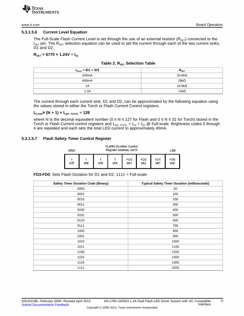
5.3.1.5.6 Current Level Equation
The Full-Scale Flash Current Level is set through the use of an external resistor (RSET) connected to theISET pin. The RSET selection equation can be used to set the current through each of the two current sinks,D1 and D2.
RSET = 6770 × 1.24V ÷ IDx
Table 2. RSET Selection Table
IFlash = ID1 + ID2 RSET
500mA 33.6kΩ600mA 28kΩ
1A 16.8kΩ1.2A 14kΩ
The current through each current sink, D1 and D2, can be approximated by the following equation usingthe values stored in either the Torch or Flash Current Control registers.
IFLASH≊≊ (N + 1) × ILED_TOTAL ÷ 128
where N is the decimal equivalent number (0 ≤ N ≤ 127 for Flash and 0 ≤ N ≤ 31 for Torch) stored in theTorch or Flash Current control registers and ILED_TOTAL = ID1 + ID2 @ Full-scale. Brightness codes 0 through4 are repeated and each sets the total LED current to approximately 40mA.
5.3.1.5.7 Flash Safety Timer Control Register
FD3-FD0: Sets Flash Duration for D1 and D2. 1111 = Full-scale
Safety Timer Duration Code (Binary) Typical Safety Timer Duration (milliseconds)
0000 50
0001 100
0010 200
0011 300
0100 400
0101 500
0110 600
0111 700
1000 800
1001 900
1010 1000
1011 1100
1100 1200
1101 1300
1110 1400
1111 3200
9SNVA319B–February 2008–Revised April 2013 AN-1780 LM3553 1.2A Dual Flash LED Driver System with I2C CompatibleInterfaceSubmit Documentation Feedback
Copyright © 2008–2013, Texas Instruments Incorporated
Board Operation www.ti.com
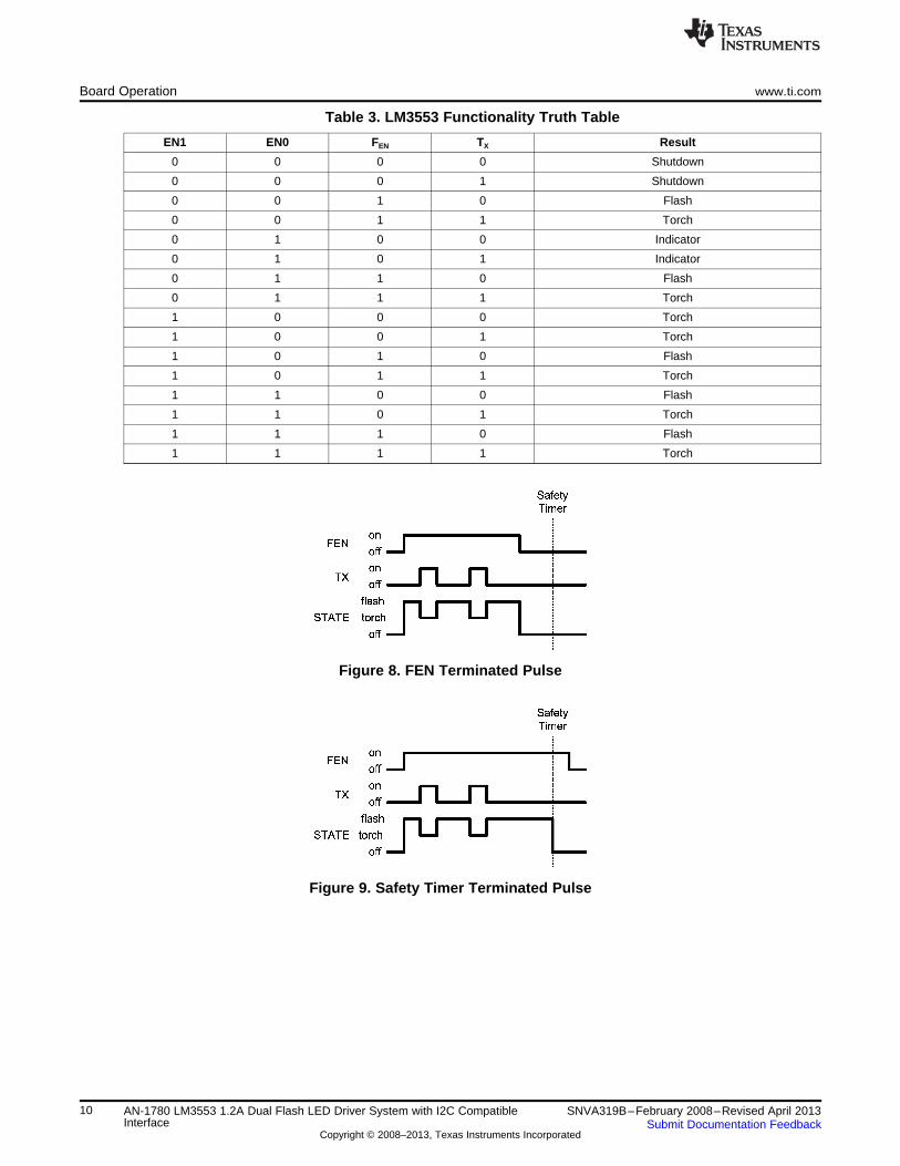
Table 3. LM3553 Functionality Truth Table
EN1 EN0 FEN TX Result
0 0 0 0 Shutdown
0 0 0 1 Shutdown
0 0 1 0 Flash
0 0 1 1 Torch
0 1 0 0 Indicator
0 1 0 1 Indicator
0 1 1 0 Flash
0 1 1 1 Torch
1 0 0 0 Torch
1 0 0 1 Torch
1 0 1 0 Flash
1 0 1 1 Torch
1 1 0 0 Flash
1 1 0 1 Torch
1 1 1 0 Flash
1 1 1 1 Torch
Figure 8. FEN Terminated Pulse
Figure 9. Safety Timer Terminated Pulse
10 AN-1780 LM3553 1.2A Dual Flash LED Driver System with I2C Compatible SNVA319B–February 2008–Revised April 2013Interface Submit Documentation Feedback
Copyright © 2008–2013, Texas Instruments Incorporated

www.ti.com Software Interface Information
Figure 10. TX Terminated Pulse
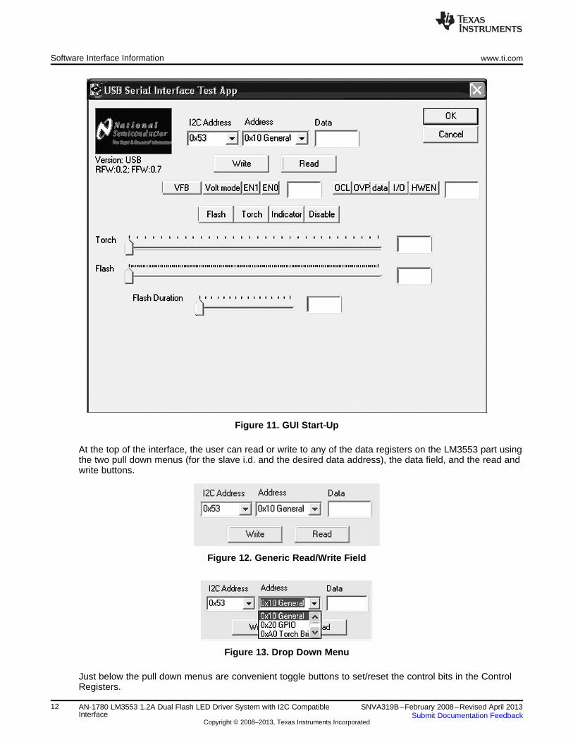
6 Software Interface Information
In order to fully evaluate the LM3553 part, an “I2C Compatible” interface must be used for any functionalityto occur. A detailed description of the interface control is described in the LM3553 data sheet.
TI has created an I2C compatible interface generation program and USB docking board that can helpexercise the part in a simple way. Contained in this document is a description of how to use the USBdocking board and interface software.
The LM3553 evaluation board has the means to “plug into” the USB docking board. The USB dockingboard provides all of the control signals for the simple interface. Power to the part must be providedexternally. A standard USB cable must be connected to the board from a PC.
The I2C compatible interface program provides all of the control that the LM3553 part requires. For properoperation, the USB docking board should be plugged into the PC before the interface program is opened.Once connected, and the program is executed, a basic interface window will open.
11SNVA319B–February 2008–Revised April 2013 AN-1780 LM3553 1.2A Dual Flash LED Driver System with I2C CompatibleInterfaceSubmit Documentation Feedback
Copyright © 2008–2013, Texas Instruments Incorporated
Software Interface Information www.ti.com
Figure 11. GUI Start-Up
At the top of the interface, the user can read or write to any of the data registers on the LM3553 part usingthe two pull down menus (for the slave i.d. and the desired data address), the data field, and the read andwrite buttons.
Figure 12. Generic Read/Write Field
Figure 13. Drop Down Menu
Just below the pull down menus are convenient toggle buttons to set/reset the control bits in the ControlRegisters.
12 AN-1780 LM3553 1.2A Dual Flash LED Driver System with I2C Compatible SNVA319B–February 2008–Revised April 2013Interface Submit Documentation Feedback
Copyright © 2008–2013, Texas Instruments Incorporated

www.ti.com Software Interface Information
• VFB: Toggles the Feedback voltage between 450mV (default) and 350mV. When pressed, thefeedback voltage will be set to 350mV
• Volt Mode: Places the LM3553 into voltage output mode. When depressed, the part will output 4.98V.
• EN1 and EN0: These bits place the part into either shutdown, indicator, torch or flash. '00' = Shutdown,'01'=Indicator, '10'=Torch, '11'=Flash.
• OCL: Toggles the inductor current limit between 2.5A (default) and 1.7A. When the OCL button isdepressed, the current limit will be set to 1.7A
• OVP: Toggles the over-voltage protection level between 5.6V (default) and 18.9V. When the OVPbutton is depressed, the OVP level will be set to 18.9V
• Data, I/O, HWEN: These buttons control the functionality of the M/F pin. Please refer to the M/F pindescription for a detailed description of the M/F pin operation.
• Flash: Starts a Flash event by setting the EN1 and EN0 bits to 1's.
• Torch: Starts a Torch event by setting the EN1 bit to a '1' and EN 0 bit to a '0'.
• Indicator: Starts an Indicator event by setting the EN1 bit to a '0' and EN 0 bit to a '1'.
• Disable: Shuts down the LM3553 by setting the EN1 and EN0 bits to 0's.
• Torch Slider: Sets the Torch brightness to any allowable brightness code (0 to 31)
• Flash Slider: Sets the Flash brightness to any allowable brightness code (0 to 127)
• Flash Duration: Sets the Flash duration to one of the 16 built-in time durations (0 to 15)
NOTE: If the part is enabled to any level of brightness or state and the program is closed (by eitherhitting the OK or cancel buttons) , the LM3553 part will remain in the last controlled state.
13SNVA319B–February 2008–Revised April 2013 AN-1780 LM3553 1.2A Dual Flash LED Driver System with I2C CompatibleInterfaceSubmit Documentation Feedback
Copyright © 2008–2013, Texas Instruments Incorporated

IMPORTANT NOTICE
Texas Instruments Incorporated and its subsidiaries (TI) reserve the right to make corrections, enhancements, improvements and otherchanges to its semiconductor products and services per JESD46, latest issue, and to discontinue any product or service per JESD48, latestissue. Buyers should obtain the latest relevant information before placing orders and should verify that such information is current andcomplete. All semiconductor products (also referred to herein as “components”) are sold subject to TI’s terms and conditions of salesupplied at the time of order acknowledgment.
TI warrants performance of its components to the specifications applicable at the time of sale, in accordance with the warranty in TI’s termsand conditions of sale of semiconductor products. Testing and other quality control techniques are used to the extent TI deems necessaryto support this warranty. Except where mandated by applicable law, testing of all parameters of each component is not necessarilyperformed.
TI assumes no liability for applications assistance or the design of Buyers’ products. Buyers are responsible for their products andapplications using TI components. To minimize the risks associated with Buyers’ products and applications, Buyers should provideadequate design and operating safeguards.
TI does not warrant or represent that any license, either express or implied, is granted under any patent right, copyright, mask work right, orother intellectual property right relating to any combination, machine, or process in which TI components or services are used. Informationpublished by TI regarding third-party products or services does not constitute a license to use such products or services or a warranty orendorsement thereof. Use of such information may require a license from a third party under the patents or other intellectual property of thethird party, or a license from TI under the patents or other intellectual property of TI.
Reproduction of significant portions of TI information in TI data books or data sheets is permissible only if reproduction is without alterationand is accompanied by all associated warranties, conditions, limitations, and notices. TI is not responsible or liable for such altereddocumentation. Information of third parties may be subject to additional restrictions.
Resale of TI components or services with statements different from or beyond the parameters stated by TI for that component or servicevoids all express and any implied warranties for the associated TI component or service and is an unfair and deceptive business practice.TI is not responsible or liable for any such statements.
Buyer acknowledges and agrees that it is solely responsible for compliance with all legal, regulatory and safety-related requirementsconcerning its products, and any use of TI components in its applications, notwithstanding any applications-related information or supportthat may be provided by TI. Buyer represents and agrees that it has all the necessary expertise to create and implement safeguards whichanticipate dangerous consequences of failures, monitor failures and their consequences, lessen the likelihood of failures that might causeharm and take appropriate remedial actions. Buyer will fully indemnify TI and its representatives against any damages arising out of the useof any TI components in safety-critical applications.
In some cases, TI components may be promoted specifically to facilitate safety-related applications. With such components, TI’s goal is tohelp enable customers to design and create their own end-product solutions that meet applicable functional safety standards andrequirements. Nonetheless, such components are subject to these terms.
No TI components are authorized for use in FDA Class III (or similar life-critical medical equipment) unless authorized officers of the partieshave executed a special agreement specifically governing such use.
Only those TI components which TI has specifically designated as military grade or “enhanced plastic” are designed and intended for use inmilitary/aerospace applications or environments. Buyer acknowledges and agrees that any military or aerospace use of TI componentswhich have not been so designated is solely at the Buyer's risk, and that Buyer is solely responsible for compliance with all legal andregulatory requirements in connection with such use.
TI has specifically designated certain components as meeting ISO/TS16949 requirements, mainly for automotive use. In any case of use ofnon-designated products, TI will not be responsible for any failure to meet ISO/TS16949.
Products Applications
Audio www.ti.com/audio Automotive and Transportation www.ti.com/automotive
Amplifiers amplifier.ti.com Communications and Telecom www.ti.com/communications
Data Converters dataconverter.ti.com Computers and Peripherals www.ti.com/computers
DLP® Products www.dlp.com Consumer Electronics www.ti.com/consumer-apps
DSP dsp.ti.com Energy and Lighting www.ti.com/energy
Clocks and Timers www.ti.com/clocks Industrial www.ti.com/industrial
Interface interface.ti.com Medical www.ti.com/medical
Logic logic.ti.com Security www.ti.com/security
Power Mgmt power.ti.com Space, Avionics and Defense www.ti.com/space-avionics-defense
Microcontrollers microcontroller.ti.com Video and Imaging www.ti.com/video
RFID www.ti-rfid.com
OMAP Applications Processors www.ti.com/omap TI E2E Community e2e.ti.com
Wireless Connectivity www.ti.com/wirelessconnectivity
Mailing Address: Texas Instruments, Post Office Box 655303, Dallas, Texas 75265Copyright © 2013, Texas Instruments Incorporated