lm284x and lm284x-q1 100, 300, or 600-ma 42-v input step ... · pdf file1 cb i sw fet gate...
TRANSCRIPT

FBGND
SW
CB
SHDN
LM2840/1/2-ADJL
VOUT
VIN
L1
D1
R1
R2
VIN
CBOOT
CIN COUT
Copyright © 2016, Texas Instruments Incorporated
Product
Folder
Order
Now
Technical
Documents
Tools &
Software
Support &Community
ReferenceDesign
An IMPORTANT NOTICE at the end of this data sheet addresses availability, warranty, changes, use in safety-critical applications,intellectual property matters and other important disclaimers. PRODUCTION DATA.
LM2840-Q1, LM2841-Q1, LM2842-Q1LM2841, LM2842, LM2840
SNVS540J –MARCH 2009–REVISED FEBRUARY 2017
LM284x and LM284x-Q1 100, 300, or 600-mA 42-V Input Step-DownDC-DC Regulator in Thin SOT
1
1 Features1• LM2840-Q1, LM2841-Q1, and LM2842-Q1 are
Qualified for Automotive Applications• AEC-Q100 Test Guidance With the Following:
– Device Temperature Grade 1: –40°C to 125°CAmbient Operating Temperature
– Device HBM ESD Classification Level 2• Input Voltage Range of 4.5 V to 42 V• Output Current Options of 100 mA, 300 mA, and
600 mA• Feedback Pin Voltage of 0.765 V• 550-kHz (X) or 1.25-MHz (Y) Switching Frequency• Low Shutdown IQ: 16-µA Typical• Short-Circuit Protected• Internally Compensated• Soft-Start Circuitry• Small Overall Solution Size (SOT-6L Package)• Create a Custom Design Using the LM2840 With
the WEBENCH® Power Designer•2 Applications• Battery-Powered Equipment• Industrial Distributed Power Applications• Portable Media Players• Portable Hand-Held Instruments
3 DescriptionThe LM284x and LM284x-Q1 devices are PWMDC‑DC buck (step-down) regulators. With an inputrange from 4.5 V to 42 V, they are suitable for a widerange of applications, such as power conditioningfrom unregulated sources. They feature a low RDSON(0.9‑Ω typical) internal switch for maximum efficiency(85% typical). Operating frequency is fixed at550 kHz (X option) and 1.25 MHz (Y option), allowingthe use of small external components while still beingable to have low output voltage ripple. Soft start canbe implemented using the Shutdown (SHDN) pin withan external RC circuit allowing the user to tailor thesoft-start time to a specific application.
The LM2840 and LM2840-Q1 are optimized for up to100 mA, the LM2841 and LM2841-Q1 for up to300 mA, and the LM2842 and LM2842-Q1 for up to600‑mA load currents. They all have a 0.765-Vnominal feedback voltage.
Additional features include: thermal shutdown, VINundervoltage lockout, and gate drive undervoltagelockout. The LM284x and LM284x-Q1 are available ina low-profile SOT-6L package.
Device Information(1)
PART NUMBER PACKAGE BODY SIZE (NOM)LM2840, LM2840-Q1,LM2841, LM2841-Q1,LM2842, LM2842-Q1
SOT (6) 1.60 mm × 2.90 mm
(1) For all available packages, see the orderable addendum atthe end of the data sheet.
Typical Application Circuit

2
LM2840-Q1, LM2841-Q1, LM2842-Q1LM2841, LM2842, LM2840SNVS540J –MARCH 2009–REVISED FEBRUARY 2017 www.ti.com
Product Folder Links: LM2840-Q1 LM2841-Q1 LM2842-Q1 LM2841 LM2842 LM2840
Submit Documentation Feedback Copyright © 2009–2017, Texas Instruments Incorporated
Table of Contents1 Features .................................................................. 12 Applications ........................................................... 13 Description ............................................................. 14 Revision History..................................................... 25 Pin Configuration and Functions ......................... 36 Specifications......................................................... 3
6.1 Absolute Maximum Ratings ..................................... 36.2 ESD Ratings.............................................................. 36.3 Recommended Operating Conditions....................... 46.4 Thermal Information .................................................. 46.5 Electrical Characteristics .......................................... 46.6 Typical Characteristics .............................................. 6
7 Detailed Description .............................................. 87.1 Overview ................................................................... 87.2 Functional Block Diagram ......................................... 87.3 Feature Description................................................... 87.4 Device Functional Modes.......................................... 9
8 Application and Implementation ........................ 10
8.1 Application Information............................................ 108.2 Typical Applications ................................................ 10
9 Power Supply Recommendations ...................... 1510 Layout................................................................... 16
10.1 Layout Guidelines ................................................. 1610.2 Layout Example .................................................... 16
11 Device and Documentation Support ................. 1711.1 Custom Design With WEBENCH® Tools ............. 1711.2 Device Support...................................................... 1711.3 Documentation Support ........................................ 1711.4 Related Links ........................................................ 1711.5 Receiving Notification of Documentation Updates 1711.6 Community Resources.......................................... 1811.7 Trademarks ........................................................... 1811.8 Electrostatic Discharge Caution............................ 1811.9 Glossary ................................................................ 18
12 Mechanical, Packaging, and OrderableInformation ........................................................... 18
4 Revision HistoryNOTE: Page numbers for previous revisions may differ from page numbers in the current version.
Changes from Revision I (September 2016) to Revision J Page
• Added this new text for Pin 4.................................................................................................................................................. 3• Added this new line of text in Shutdown Operation section ................................................................................................. 12
Changes from Revision H (April 2013) to Revision I Page
• Added ESD Ratings table, Feature Description section, Device Functional Modes, Application and Implementationsection, Power Supply Recommendations section, Layout section, Device and Documentation Support section, andMechanical, Packaging, and Orderable Information section. ................................................................................................. 1
• Added Thermal Information table ........................................................................................................................................... 4
Changes from Revision G (April 2013) to Revision H Page
• Changed layout of National Semiconductor Data Sheet to TI format .................................................................................... 1

1CB 6 SW
2GND 5 VIN
3FB 4 SHDN
Not to scale
3
LM2840-Q1, LM2841-Q1, LM2842-Q1LM2841, LM2842, LM2840
www.ti.com SNVS540J –MARCH 2009–REVISED FEBRUARY 2017
Product Folder Links: LM2840-Q1 LM2841-Q1 LM2842-Q1 LM2841 LM2842 LM2840
Submit Documentation FeedbackCopyright © 2009–2017, Texas Instruments Incorporated
5 Pin Configuration and Functions
DDC Package6-Pin SOTTop View
Pin FunctionsPIN
I/O DESCRIPTIONNO. NAME1 CB I SW FET gate bias voltage. Connect CBOOT capacitor between CB and SW.2 GND — Ground connection
3 FB I Feedback pin: Set feedback voltage divider ratio with VOUT = VFB (1 + (R1 / R2)). Resistors must be from100 Ω to 10 kΩ to avoid input bias errors.
4 SHDN I Logic level shutdown input. Pull to GND to disable the device and pull high to enable the device. If this functionis not used tie to VIN . DO NOT ALLOW TO FLOAT.
5 VIN I Power input voltage pin: 4.5-V to 42-V normal operating range.6 SW O Power FET output: Connect to inductor, diode, and CBOOT capacitor.
(1) Stresses beyond those listed under Absolute Maximum Ratings may cause permanent damage to the device. These are stress ratingsonly, which do not imply functional operation of the device at these or any other conditions beyond those indicated under RecommendedOperating Conditions. Exposure to absolute-maximum-rated conditions for extended periods may affect device reliability.
(2) If Military/Aerospace specified devices are required, please contact the Texas Instruments Sales Office/Distributors for availability andspecifications.
(3) The maximum allowable power dissipation is a function of the maximum junction temperature, TJ(MAX), the junction-to-ambient thermalresistance, RθJA, and the ambient temperature, TA. The maximum allowable power dissipation at any ambient temperature is calculatedusing: PD (MAX) = (TJ(MAX) − TA)/RθJA. Exceeding the maximum allowable power dissipation causes excessive die temperature, and theregulator goes into thermal shutdown. Internal thermal shutdown circuitry protects the device from permanent damage. Thermalshutdown engages at TJ=175°C (typical) and disengages at TJ= 155°C (typical).
6 Specifications
6.1 Absolute Maximum RatingsSee (1) (2)
MIN MAX UNITVIN –0.3 45 VSHDN –0.3 (VIN + 0.3 V) < 45 VSW voltage –0.3 45 VCB voltage above SW voltage 7 VFB voltage –0.3 5 VPower dissipation (3) Internally LimitedMaximum junction temperature 150 °CStorage temperature, Tstg –65 150 °C
(1) JEDEC document JEP155 states that 500-V HBM allows safe manufacturing with a standard ESD control process.
6.2 ESD RatingsVALUE UNIT
V(ESD) Electrostatic discharge Human-body model (HBM), per ANSI/ESDA/JEDEC JS-001 (1) ±2000 V

4
LM2840-Q1, LM2841-Q1, LM2842-Q1LM2841, LM2842, LM2840SNVS540J –MARCH 2009–REVISED FEBRUARY 2017 www.ti.com
Product Folder Links: LM2840-Q1 LM2841-Q1 LM2842-Q1 LM2841 LM2842 LM2840
Submit Documentation Feedback Copyright © 2009–2017, Texas Instruments Incorporated
(1) All limits specified at room temperature (TA = 25°C) unless otherwise specified. All room temperature limits are 100% production tested.All limits at temperature extremes are ensured through correlation using standard Statistical Quality Control (SQC) methods. All limitsare used to calculate Average Outgoing Quality Level (AOQL).
6.3 Recommended Operating Conditionsover operating free-air temperature range (unless otherwise noted)
MIN MAX UNITOperating junction temperature (1) –40 125 °CInput voltage VIN 4.5 42 VSW voltage 42 V
(1) For more information about traditional and new thermal metrics, see the Semiconductor and IC Package Thermal Metrics applicationreport.
(2) The package thermal impedance is calculated in accordance to JESD 51-7.(3) Thermal Resistances were simulated on a 4-layer, JEDEC board
6.4 Thermal Information
THERMAL METRIC (1)LM284x, LM284x-Q1
UNITDDC (SOT)6 PINS
RθJA Junction-to-ambient thermal resistance (2) (3) 121 °C/WRθJC(top) Junction-to-case (top) thermal resistance 94 °C/W
(1) All limits specified at room temperature (TA = 25°C) unless otherwise noted. Room temperature limits are production tested. Limits attemperature extremes are ensured through correlation using standard Statistical Quality Control (SQC) methods. Limits are used tocalculate Average Outgoing Quality Level (AOQL).
(2) Typical numbers are at 25°C and represent the most likely norm.(3) The part numbers in this table represent both the Q1 and non-Q1 versions of the respective parts.(4) Includes the bond wires, RDSON from VIN pin to SW pin.(5) Current limit at 0% duty cycle. May be lower at higher duty cycle or input voltages below 6 V.(6) Bias currents flow into pin.
6.5 Electrical CharacteristicsSpecifications are for TJ = 25°C unless otherwise specified. Minimum and Maximum limits are specified through test, design,or statistical correlation. Typical values represent the most likely parametric norm at TJ = 25°C, and are provided for referencepurposes only. Unless otherwise stated the following conditions apply: VIN = 12 V. (1) (2) (3)
PARAMETER TEST CONDITIONS MIN TYP MAX UNIT
IQ Quiescent current
SHDN = 0 V16
µATJ = −40°C to 125°C 40
Device ON, not switching1.3
mATJ = −40°C to 125°C 1.75
Device ON, no load1.35
TJ = −40°C to 125°C 1.85
RDSON Switch ON resistance See (4) 0.9Ω
TJ = −40°C to 125°C 1.6
ILSW Switch leakage current VIN = 42 V0
µATJ = −40°C to 125°C 0.5
ICL Switch current limit
LM2840 (5) 525mA
TJ = −40°C to 125°C 900
LM2841 (5) 525mA
TJ = −40°C to 125°C 900
LM2842 (5) 1.15A
TJ = −40°C to 125°C 1.7
IFB Feedback pin bias current LM284[0,1,2] (6) 0.1µA
TJ = −40°C to 125°C 1

5
LM2840-Q1, LM2841-Q1, LM2842-Q1LM2841, LM2842, LM2840
www.ti.com SNVS540J –MARCH 2009–REVISED FEBRUARY 2017
Product Folder Links: LM2840-Q1 LM2841-Q1 LM2842-Q1 LM2841 LM2842 LM2840
Submit Documentation FeedbackCopyright © 2009–2017, Texas Instruments Incorporated
Electrical Characteristics (continued)Specifications are for TJ = 25°C unless otherwise specified. Minimum and Maximum limits are specified through test, design,or statistical correlation. Typical values represent the most likely parametric norm at TJ = 25°C, and are provided for referencepurposes only. Unless otherwise stated the following conditions apply: VIN = 12 V.(1)(2)(3)
PARAMETER TEST CONDITIONS MIN TYP MAX UNIT
(7) Minimum ON-time specified by design and simulation.
VFB FB Pin reference voltage0.765
VTJ = −40°C to 125°C 0.747 0.782
tON(min) Minimum ON-time See (7) 100ns
TJ = −40°C to 125°C 150
tOFF(min) Minimum OFF-timeX option
110ns
TJ = −40°C to 125°C 370
Y option104
nsTJ = −40°C to 125°C 200
fSW Switching frequency
X option, VFB = 0.5 V550
kHzTJ = −40°C to 125°C 325 750X option, VFB = 0 V 140
Y option, VFB = 0.5 V1.25
MHzTJ = −40°C to 125°C 0.95 1.5Y option, VFB = 0 V 0.35
DMAX Maximum duty cycleX option
94%TJ = −40°C to 125°C 88%
Y option87%
TJ = −40°C to 125°C 81%
VUVPUndervoltage lockoutthresholds
On threshold3.7
VTJ = −40°C to 125°C 4.4
Off threshold3.5
TJ = −40°C to 125°C 3.25
V SHDN Shutdown thresholdDevice ON
1
VTJ = −40°C to 125°C 2.3
Device OFF0.9
TJ = −40°C to 125°C 0.3
ISHDNShutdown pin input biascurrent
VSHDN = 2.3 V (6) 0.05
µATJ = −40°C to 125°C 1.5
VSHDN = 0 V0.02
TJ = −40°C to 125°C 1.5

SW
ITC
H C
UR
RE
NT
LIM
IT (m
A)
1.0 1.6 2.2 2.8 3.4 4.0
800
600
400
200
0
SHDN PIN VOLTAGE (V)
0
10
20
30
40
50
60
70
80
90
100
0 20 40 60 80 100 120
LOAD CURRENT (mA)
EF
FIC
IEN
CY
(%
)
VIN = 12V
VIN = 24V
0.0 0.1 0.2 0.3
LOAD CURRENT (A)
0
20
40
60
80
100
EF
FIC
IEN
CY
(%) VIN = 36V
VIN = 12V
VIN = 24V
0.0 0.1 0.2 0.3
LOAD CURRENT (A)
0
20
40
60
80
100E
FF
ICIE
NC
Y(%
)
VIN = 12V
VIN = 24V
0.4 0.5 0.6
VIN = 36V
6
LM2840-Q1, LM2841-Q1, LM2842-Q1LM2841, LM2842, LM2840SNVS540J –MARCH 2009–REVISED FEBRUARY 2017 www.ti.com
Product Folder Links: LM2840-Q1 LM2841-Q1 LM2842-Q1 LM2841 LM2842 LM2840
Submit Documentation Feedback Copyright © 2009–2017, Texas Instruments Incorporated
6.6 Typical CharacteristicsThe part numbers in this section represent both the Q1 and non-Q1 versions of the respective parts.
LM2842X VOUT = 3.3 V
Figure 1. Efficiency vs Load Current
LM2841X VOUT = 3.3 V
Figure 2. Efficiency vs Load Current
LM2840X VOUT = 8 V
Figure 3. Efficiency vs Load Current
X option
Figure 4. Switching Frequency vs Temperature
Figure 5. Input UVLO Voltage vs Temperature
Soft-Start Implementation LM284[0,1]
Figure 6. Switch Current Limit vs SHDN Pin Voltage

SW
ITC
H C
UR
RE
NT
LIM
IT (A
)
1.1 1.7 2.3 2.8 3.4 4.0
SHDN PIN VOLTAGE (V)
1.2
1.0
0.9
0.7
0.6
0.4
7
LM2840-Q1, LM2841-Q1, LM2842-Q1LM2841, LM2842, LM2840
www.ti.com SNVS540J –MARCH 2009–REVISED FEBRUARY 2017
Product Folder Links: LM2840-Q1 LM2841-Q1 LM2842-Q1 LM2841 LM2842 LM2840
Submit Documentation FeedbackCopyright © 2009–2017, Texas Instruments Incorporated
Typical Characteristics (continued)The part numbers in this section represent both the Q1 and non-Q1 versions of the respective parts.
Soft-Start Implementation LM2842
Figure 7. Switch Current Limit vs SHDN Pin Voltage Figure 8. SHDN Pin Current vs SHDN Pin Voltage

Max DutyCycle Limit
OSC
DCLIMIT
SET
++
-
+PWMComp RESET
FETDriver
BUCKDRIVE
+
-ErrorAmp
FB
BandgapSoftStart
ThermalShutdown
TSD
SHDN
InductorCurrent
Measurement
CB
SW
GND
UVLOComp
BG
UVLO
VoltageRegulator
VIN
Copyright © 2016, Texas Instruments Incorporated
8
LM2840-Q1, LM2841-Q1, LM2842-Q1LM2841, LM2842, LM2840SNVS540J –MARCH 2009–REVISED FEBRUARY 2017 www.ti.com
Product Folder Links: LM2840-Q1 LM2841-Q1 LM2842-Q1 LM2841 LM2842 LM2840
Submit Documentation Feedback Copyright © 2009–2017, Texas Instruments Incorporated
7 Detailed Description
7.1 OverviewThe LM284x and LM284x-Q1 SIMPLE SWITCHER® regulators are easy-to-use, non-synchronous, step-downDC-DC converters with a wide input voltage range up to 42 V. The devices are capable of delivering up to100‑mA, 300-mA, or 600-mA DC load current with excellent line and load regulation. These devices are availablein fixed frequency of 550 kHz and 1.25 MHz. The family requires few external components, and the pinarrangement was designed for simple, optimum PCB layout.
7.2 Functional Block Diagram
7.3 Feature Description
7.3.1 ProtectionThe LM284x and LM284x-Q1 have dedicated protection circuitry running during normal operation to protect theIC. The thermal shutdown circuitry turns off the power device when the die temperature reaches excessivelevels. The UVLO comparator protects the power device during supply power start-up and shutdown to preventoperation at voltages less than the minimum input voltage. A gate drive (CB) undervoltage lockout is included toensure that there is enough gate drive voltage to drive the MOSFET before the device tries to start switching.The LM284x and LM284x-Q1 also feature a shutdown mode decreasing the supply current to approximately16 µA.
9
LM2840-Q1, LM2841-Q1, LM2842-Q1LM2841, LM2842, LM2840
www.ti.com SNVS540J –MARCH 2009–REVISED FEBRUARY 2017
Product Folder Links: LM2840-Q1 LM2841-Q1 LM2842-Q1 LM2841 LM2842 LM2840
Submit Documentation FeedbackCopyright © 2009–2017, Texas Instruments Incorporated
7.4 Device Functional Modes
7.4.1 Continuous Conduction ModeThe LM284x and LM284x-Q1 contain a current-mode, PWM buck regulator. A buck regulator steps the inputvoltage down to a lower output voltage. In continuous conduction mode (when the inductor current never reacheszero at steady-state operation), the buck regulator operates in two cycles. The power switch is connectedbetween VIN and SW. In the first cycle of operation the transistor is closed and the diode is reverse biased.Energy is collected in the inductor and the load current is supplied by COUT and the rising current through theinductor. During the second cycle the transistor is open and the diode is forward biased due to the fact that theinductor current cannot instantaneously change direction. The energy stored in the inductor is transferred to theload and output capacitor. The ratio of these two cycles determines the output voltage. The output voltage isdefined approximately as shown in Equation 1.
D = VOUT / VIN (1)D’ = (1 – D)
where• D is the duty cycle of the switch (2)
D and D' are required for design calculations.

FBGND
SW
CB
SHDN
LM2840/1/2-ADJL
3.3V OUT
4.5V to 42V IND1MA2YD26
R1
3.4k
R21.02k
CBOOT
VIN
CIN
2.2 PF
0.1 PF
L115 PH
COUT
10 PF
Copyright © 2016, Texas Instruments Incorporated
10
LM2840-Q1, LM2841-Q1, LM2842-Q1LM2841, LM2842, LM2840SNVS540J –MARCH 2009–REVISED FEBRUARY 2017 www.ti.com
Product Folder Links: LM2840-Q1 LM2841-Q1 LM2842-Q1 LM2841 LM2842 LM2840
Submit Documentation Feedback Copyright © 2009–2017, Texas Instruments Incorporated
8 Application and Implementation
NOTEInformation in the following applications sections is not part of the TI componentspecification, and TI does not warrant its accuracy or completeness. TI’s customers areresponsible for determining suitability of components for their purposes. Customers shouldvalidate and test their design implementation to confirm system functionality.
8.1 Application InformationThe LM284x and LM284x-Q1 are step-down DC-DC regulators. It is typically used to convert a higher DC voltageto a lower DC voltage with a maximum output current of 100 mA, 300 mA, or 600 mA. The following designprocedure can be used to select components for the LM284x and LM284x-Q1. Alternately, the WEBENCH®
software may be used to generate complete designs. When generating a design, the WEBENCH software usesiterative design procedure and accesses comprehensive databases of components. See ti.com for more details
8.2 Typical Applications
8.2.1 Step-Down Converter With 3.3-V Output Voltage
Figure 9. Application Circuit, 3.3-V Output at 100 mA
8.2.1.1 Design RequirementsTable 1 lists the design parameters for this example.
Table 1. Design ParametersDESIGN PARAMETER EXAMPLE VALUE
Input voltage 4.5 V to 42 VOutput voltage 3.3 VOutput current 0.1 A
8.2.1.2 Detailed Design Procedure
8.2.1.2.1 Custom Design With WEBENCH® Tools
Click here to create a custom design using the LM2840 device with the WEBENCH® Power Designer.1. Start by entering the input voltage (VIN), output voltage (VOUT), and output current (IOUT) requirements.2. Optimize the design for key parameters such as efficiency, footprint, and cost using the optimizer dial.3. Compare the generated design with other possible solutions from Texas Instruments.
The WEBENCH Power Designer provides a customized schematic along with a list of materials with real-timepricing and component availability.
In most cases, these actions are available:

L =(VIN - VOUT)VOUT
VIN x IRIPPLE x fSW
11
LM2840-Q1, LM2841-Q1, LM2842-Q1LM2841, LM2842, LM2840
www.ti.com SNVS540J –MARCH 2009–REVISED FEBRUARY 2017
Product Folder Links: LM2840-Q1 LM2841-Q1 LM2842-Q1 LM2841 LM2842 LM2840
Submit Documentation FeedbackCopyright © 2009–2017, Texas Instruments Incorporated
• Run electrical simulations to see important waveforms and circuit performance• Run thermal simulations to understand board thermal performance• Export customized schematic and layout into popular CAD formats• Print PDF reports for the design, and share the design with colleagues
Get more information about WEBENCH tools at www.ti.com/WEBENCH.
This section presents guidelines for selecting external components.
8.2.1.2.2 Setting the Output Voltage
The output voltage is set using the feedback pin and a resistor divider connected to the output as shown inTypical Application Circuit. The feedback pin voltage 0.765 V, so the ratio of the feedback resistors sets theoutput voltage according to Equation 3:
VOUT = 0.765 V (1 + (R1 / R2)) (3)
Typically R2 is given as 100 Ω to 10 kΩ for a starting value. To solve for R1 given R2 and VOUT, use Equation 4:R1 = R2 ((VOUT / 0.765 V) – 1) (4)
8.2.1.2.3 Inductor Selection
The most critical parameters for the inductor are the inductance, peak current, and the DC resistance. Theinductance is related to the peak-to-peak inductor ripple current, the input and the output voltages.
(5)
A higher value of ripple current reduces inductance, but increases the conductance loss, core loss, and currentstress for the inductor and switch devices. It also requires a bigger output capacitor for the same output voltageripple requirement. A reasonable value is setting the ripple current to be 30% of the DC output current. Becausethe ripple current increases with the input voltage, the maximum input voltage is always used to determine theinductance. The DC resistance of the inductor is a key parameter for the efficiency. Lower DC resistance isavailable with a bigger winding area. A good tradeoff between the efficiency and the core size is letting theinductor copper loss equal 2% of the output power. See Selecting Inductors for Buck Converters for moreinformation on selecting inductors. A good starting point for most applications is a 10 µH to 22 µH with 1.1 A orgreater current rating for the LM2842 and LM2842-Q1 or a 0.7 A or greater current rating for the LM284x andLM284x-Q1. Using such a rating enables the device to current limit without saturating the inductor. This ispreferable to the device going into thermal shutdown mode and the possibility of damaging the inductor if theoutput is shorted to ground or other long-term overload.
Table 2. Recommended InductorsMANUFACTURER INDUCTOR CONTACT INFORMATION
Coilcraft LPS4018, DO1608C, DO3308, and LPO2506 series www.coilcraft.com800-3222645
MuRata LQH55D and LQH66S series www.murata.comCoiltronics MP2 and MP2A series www.cooperbussman.com
8.2.1.2.4 Input Capacitor
A low ESR ceramic capacitor ©IN) is needed between the VIN pin and GND pin. This capacitor prevents largevoltage transients from appearing at the input. Use a 2.2-µF to 10-µF value with X5R or X7R dielectric.Depending on construction, a ceramic capacitor’s value can decrease up to 50% of its nominal value when ratedvoltage is applied. Consult with the capacitor manufacturer's data sheet for information on capacitor derating overvoltage and temperature.
8.2.1.2.5 Output Capacitor
The selection of COUT is driven by the maximum allowable output voltage ripple. The output ripple in the constantfrequency, PWM mode is approximated by Equation 6.
VRIPPLE = IRIPPLE (ESR + (1 / (8fSWCOUT))) (6)

12
LM2840-Q1, LM2841-Q1, LM2842-Q1LM2841, LM2842, LM2840SNVS540J –MARCH 2009–REVISED FEBRUARY 2017 www.ti.com
Product Folder Links: LM2840-Q1 LM2841-Q1 LM2842-Q1 LM2841 LM2842 LM2840
Submit Documentation Feedback Copyright © 2009–2017, Texas Instruments Incorporated
The ESR term usually plays the dominant role in determining the voltage ripple. Low-ESR ceramic capacitors arerecommended. Capacitors in the range of 22 µF to 100 µF are a good starting point with an ESR of 0.1 Ω orless.
Table 3. Recommended Input and Output CapacitorsMANUFACTURER CAPACITOR CONTACT INFORMATION
Vishay Sprague 293D, 592D, and 595D series tantalum www.vishay.com407-324-4140
Taiyo Yuden High capacitance MLCC ceramic www.t-yuden.com408-573-4150
Cornell Dubilier ESRD seriec Polymer Aluminum ElectrolyticSPV and AFK series V-chip series www.cde.com
MuRata High capacitance MLCC ceramic www.murata.com
8.2.1.2.6 Bootstrap Capacitor
A 0.15-µF ceramic capacitor or larger is recommended for the bootstrap capacitor ©BOOT). For applications wherethe input voltage is less than twice the output voltage a larger capacitor is recommended, generally 0.15 µF to 1µF to ensure plenty of gate drive for the internal switches and a consistently low RDSON.
8.2.1.2.7 Soft-Start Components
The LM284x and LM284x-Q1 have circuitry that is used in conjunction with the SHDN pin to limit the inrushcurrent on start-up of the DC-DC switching regulator. The SHDN pin in conjunction with a RC filter is used totailor the soft start for a specific application. When a voltage applied to the SHDN pin is between 0 V and up to2.3 V it causes the cycle-by-cycle current limit in the power stage to be modulated for minimum current limit at0 V up to the rated current limit at 2.3 V. Thus controlling the output rise time and inrush current at start-up. Theresistor value must be selected so the current injected into the SHDN pin is greater then the leakage current ofthe SHDN pin (1.5 µA) when the voltage at SHDN is equal or greater then 2.3 V.
8.2.1.2.8 Shutdown Operation
The SHDN pin of the LM284x and LM284x-Q1 is designed so that it may be controlled using 2.3 V or higher logicsignals. If the shutdown function is not to be used the SHDN pin may be tied to VIN. This input should not beallowed to float
The maximum voltage to the SHDN pin should not exceed 42 V. If the use of a higher voltage is desired due tosystem or other constraints it may be used; however, a 100 kΩ or larger resistor is recommended between theapplied voltage and the SHDN pin to protect the device.
8.2.1.2.9 Schottky Diode
The breakdown voltage rating of the diode (D1) is preferred to be 25% higher than the maximum input voltage.The current rating for the diode must be equal to the maximum output current for best reliability in mostapplications. In cases where the duty cycle is greater than 50%, the average diode current is lower. In this case itis possible to use a diode with a lower average current rating, approximately (1 – D)IOUT; however, the peakcurrent rating should be higher than the maximum load current. A 0.5-A to 1-A rated diode is a good startingpoint.

FBGND
SW
CB
SHDN
LM2840/1/2-ADJL
5V OUT
7V to 42V IN
R1
R2
5.62k
1.02k
D1MA2YD26
CBOOT
VIN
CIN
2.2 PF
L115 PH
COUT
47 PF
0.15 PF
Copyright © 2016, Texas Instruments Incorporated
13
LM2840-Q1, LM2841-Q1, LM2842-Q1LM2841, LM2842, LM2840
www.ti.com SNVS540J –MARCH 2009–REVISED FEBRUARY 2017
Product Folder Links: LM2840-Q1 LM2841-Q1 LM2842-Q1 LM2841 LM2842 LM2840
Submit Documentation FeedbackCopyright © 2009–2017, Texas Instruments Incorporated
8.2.1.3 Application Curves
VIN = 12 V IOUT = 200 mAVOUT = 3.3 V Top trace: VOUT, 10 mV/div, AC-CoupledT = 1 µs/div Bottom trace: SW, 5 V/div, DC-Coupled
Figure 10. Switching Node and Output Voltage Waveforms
VIN = 12 V IOUT = 300 mA to 200 mA to 300 mAVOUT = 3.3 V Top trace: VOUT, 20 mV/div, AC-Coupled
T = 200 µs/div Bottom trace: IOUT, 100 mA/div, DC-Coupled
Figure 11. Load Transient Waveforms
VIN = 12 V IOUT = 50 mAVOUT = 3.3 V Top trace: VOUT, 1V/div, DC-CoupledT = 40 µs/div Bottom trace: SHDN, 2V/div, DC-Coupled
Figure 12. Start-Up Waveform
8.2.2 Other Application CircuitsFigure 13 to Figure 16 show application circuit examples using the LM284x and LM284x-Q1 devices. Customersmust fully validate and test these circuits before implementing a design based on these examples. Unlessotherwise noted, the design procedures in Step-Down Converter With 3.3-V Output Voltage are applicable tothese designs.
Figure 13. Step-Down Converter With 5-V Output Voltage

FBGND
SW
CB
SHDN
LM2840/1/2-ADJL
0.8V OUT
4.5V to 12V IND1MA2YD26
R1
30.9
R2787
CBOOT
VIN
CIN
2.2 PF
L110 PH
COUT
100 PF
0.15 PF
Copyright © 2016, Texas Instruments Incorporated
FBGND
SW
CB
SHDN
LM2840/1/2-ADJL
15V OUT
18V to 42V IN D1MA2YD26
R1
28k
R21.5k
CBOOT
VIN
CIN
2.2 PF
L147 PH
COUT
22 PF
0.15 PF
Copyright © 2016, Texas Instruments Incorporated
FBGND
SW
CB
SHDN
LM2840/1/2-ADJL
12V OUT
15V to 42V IND1MA2YD26
R1
14.7k
R21k
CBOOT
VIN
CIN
2.2 PF
L147 PH
COUT
22 PF
0.15 PF
Copyright © 2016, Texas Instruments Incorporated
14
LM2840-Q1, LM2841-Q1, LM2842-Q1LM2841, LM2842, LM2840SNVS540J –MARCH 2009–REVISED FEBRUARY 2017 www.ti.com
Product Folder Links: LM2840-Q1 LM2841-Q1 LM2842-Q1 LM2841 LM2842 LM2840
Submit Documentation Feedback Copyright © 2009–2017, Texas Instruments Incorporated
Figure 14. Step-Down Converter With 12-V Output Voltage
Figure 15. Step-Down Converter With 15-V Output Voltage
Figure 16. Step-Down Converter With 0.8-V Output Voltage

15
LM2840-Q1, LM2841-Q1, LM2842-Q1LM2841, LM2842, LM2840
www.ti.com SNVS540J –MARCH 2009–REVISED FEBRUARY 2017
Product Folder Links: LM2840-Q1 LM2841-Q1 LM2842-Q1 LM2841 LM2842 LM2840
Submit Documentation FeedbackCopyright © 2009–2017, Texas Instruments Incorporated
9 Power Supply RecommendationsThe LM284x and LM284x-Q1 are designed to operate from an input voltage supply range between 4 V and 42 V.This input supply must be able to withstand the maximum input current and maintain a voltage above 4.5 V. Theresistance of the input supply rail must be low enough that an input current transient does not cause a drop atthe device supply voltage high enough to cause a false UVLO fault triggering and system reset. If the inputsupply is located more than a few inches from the device, additional bulk capacitance may be required inaddition to the ceramic input capacitors.

16
LM2840-Q1, LM2841-Q1, LM2842-Q1LM2841, LM2842, LM2840SNVS540J –MARCH 2009–REVISED FEBRUARY 2017 www.ti.com
Product Folder Links: LM2840-Q1 LM2841-Q1 LM2842-Q1 LM2841 LM2842 LM2840
Submit Documentation Feedback Copyright © 2009–2017, Texas Instruments Incorporated
10 Layout
10.1 Layout GuidelinesTo reduce problems with conducted noise pickup, the ground side of the feedback network should be connecteddirectly to the GND pin with its own connection. The feedback network, resistors R1 and R2, must be kept closeto the FB pin, and away from the inductor to minimize coupling noise into the feedback pin. The input bypasscapacitor CIN must be placed close to the VIN pin. This reduces copper trace resistance which effects inputvoltage ripple of the IC. The inductor L1 must be placed close to the SW pin to reduce EMI and capacitivecoupling. The output capacitor, COUT must be placed close to the junction of L1 and the diode D1. The L1, D1,and COUT trace must be as short as possible to reduce conducted and radiated noise and increase overallefficiency. The ground connection for the diode, CIN, and COUT should be as small as possible and tied to thesystem ground plane in only one spot (preferably at the COUT ground point) to minimize conducted noise in thesystem ground plane. See Layout Guidelines for Switching Power Supplies for more detail on switching powersupply layout considerations.
10.2 Layout Example
Figure 17. Recommended Layout

17
LM2840-Q1, LM2841-Q1, LM2842-Q1LM2841, LM2842, LM2840
www.ti.com SNVS540J –MARCH 2009–REVISED FEBRUARY 2017
Product Folder Links: LM2840-Q1 LM2841-Q1 LM2842-Q1 LM2841 LM2842 LM2840
Submit Documentation FeedbackCopyright © 2009–2017, Texas Instruments Incorporated
11 Device and Documentation Support
11.1 Custom Design With WEBENCH® ToolsClick here to create a custom design using the LM2840 device with the WEBENCH® Power Designer.1. Start by entering the input voltage (VIN), output voltage (VOUT), and output current (IOUT) requirements.2. Optimize the design for key parameters such as efficiency, footprint, and cost using the optimizer dial.3. Compare the generated design with other possible solutions from Texas Instruments.
The WEBENCH Power Designer provides a customized schematic along with a list of materials with real-timepricing and component availability.
In most cases, these actions are available:• Run electrical simulations to see important waveforms and circuit performance• Run thermal simulations to understand board thermal performance• Export customized schematic and layout into popular CAD formats• Print PDF reports for the design, and share the design with colleagues
Get more information about WEBENCH tools at www.ti.com/WEBENCH.
11.2 Device Support
11.2.1 Development SupportWEBENCH Design Center
11.3 Documentation Support
11.3.1 Related DocumentationFor related documentation, see the following:• AN-1197 Selecting Inductors for Buck Converters (SNVA038)• AN-1149 Layout Guidelines for Switching Power Supplies (SNVA021)
11.4 Related LinksThe table below lists quick access links. Categories include technical documents, support and communityresources, tools and software, and quick access to sample or buy.
Table 4. Related Links
PARTS PRODUCT FOLDER SAMPLE & BUY TECHNICALDOCUMENTS
TOOLS &SOFTWARE
SUPPORT &COMMUNITY
LM2841 Click here Click here Click here Click here Click hereLM2842 Click here Click here Click here Click here Click hereLM2840 Click here Click here Click here Click here Click here
LM2840-Q1 Click here Click here Click here Click here Click hereLM2841-Q1 Click here Click here Click here Click here Click hereLM2842-Q1 Click here Click here Click here Click here Click here
11.5 Receiving Notification of Documentation UpdatesTo receive notification of documentation updates, navigate to the device product folder on ti.com. In the upperright corner, click on Alert me to register and receive a weekly digest of any product information that haschanged. For change details, review the revision history included in any revised document.

18
LM2840-Q1, LM2841-Q1, LM2842-Q1LM2841, LM2842, LM2840SNVS540J –MARCH 2009–REVISED FEBRUARY 2017 www.ti.com
Product Folder Links: LM2840-Q1 LM2841-Q1 LM2842-Q1 LM2841 LM2842 LM2840
Submit Documentation Feedback Copyright © 2009–2017, Texas Instruments Incorporated
11.6 Community ResourcesThe following links connect to TI community resources. Linked contents are provided "AS IS" by the respectivecontributors. They do not constitute TI specifications and do not necessarily reflect TI's views; see TI's Terms ofUse.
TI E2E™ Online Community TI's Engineer-to-Engineer (E2E) Community. Created to foster collaborationamong engineers. At e2e.ti.com, you can ask questions, share knowledge, explore ideas and helpsolve problems with fellow engineers.
Design Support TI's Design Support Quickly find helpful E2E forums along with design support tools andcontact information for technical support.
11.7 TrademarksE2E is a trademark of Texas Instruments.WEBENCH, SIMPLE SWITCHER are registered trademarks of Texas Instruments.All other trademarks are the property of their respective owners.
11.8 Electrostatic Discharge CautionThese devices have limited built-in ESD protection. The leads should be shorted together or the device placed in conductive foamduring storage or handling to prevent electrostatic damage to the MOS gates.
11.9 GlossarySLYZ022 — TI Glossary.
This glossary lists and explains terms, acronyms, and definitions.
12 Mechanical, Packaging, and Orderable InformationThe following pages include mechanical, packaging, and orderable information. This information is the mostcurrent data available for the designated devices. This data is subject to change without notice and revision ofthis document. For browser-based versions of this data sheet, refer to the left-hand navigation.

PACKAGE OPTION ADDENDUM
www.ti.com 28-Feb-2017
Addendum-Page 1
PACKAGING INFORMATION
Orderable Device Status(1)
Package Type PackageDrawing
Pins PackageQty
Eco Plan(2)
Lead/Ball Finish(6)
MSL Peak Temp(3)
Op Temp (°C) Device Marking(4/5)
Samples
LM2840XMK-ADJL/NOPB ACTIVE SOT-23-THIN DDC 6 1000 Green (RoHS& no Sb/Br)
CU SN Level-1-260C-UNLIM -40 to 125 SE8B
LM2840XMKX-ADJL/NOPB ACTIVE SOT-23-THIN DDC 6 3000 Green (RoHS& no Sb/Br)
CU SN Level-1-260C-UNLIM -40 to 125 SE8B
LM2840XQMK/NOPB ACTIVE SOT-23-THIN DDC 6 1000 Green (RoHS& no Sb/Br)
CU SN Level-1-260C-UNLIM -40 to 125 SE9B
LM2840YMK-ADJL/NOPB ACTIVE SOT-23-THIN DDC 6 1000 Green (RoHS& no Sb/Br)
CU SN Level-1-260C-UNLIM -40 to 125 SF1B
LM2840YQMK/NOPB ACTIVE SOT-23-THIN DDC 6 1000 Green (RoHS& no Sb/Br)
CU SN Level-1-260C-UNLIM -40 to 125 SF2B
LM2840YQMKX/NOPB ACTIVE SOT-23-THIN DDC 6 3000 Green (RoHS& no Sb/Br)
CU SN Level-1-260C-UNLIM -40 to 125 SF2B
LM2841XMK-ADJL/NOPB ACTIVE SOT-23-THIN DDC 6 1000 Green (RoHS& no Sb/Br)
CU SN Level-1-260C-UNLIM -40 to 125 STFB
LM2841XMKX-ADJL/NOPB ACTIVE SOT-23-THIN DDC 6 3000 Green (RoHS& no Sb/Br)
CU SN Level-1-260C-UNLIM -40 to 125 STFB
LM2841XQMK/NOPB ACTIVE SOT-23-THIN DDC 6 1000 Green (RoHS& no Sb/Br)
CU SN Level-1-260C-UNLIM -40 to 125 SB1B
LM2841YMK-ADJL/NOPB ACTIVE SOT-23-THIN DDC 6 1000 Green (RoHS& no Sb/Br)
CU SN Level-1-260C-UNLIM -40 to 125 STTB
LM2841YMKX-ADJL/NOPB ACTIVE SOT-23-THIN DDC 6 3000 Green (RoHS& no Sb/Br)
CU SN Level-1-260C-UNLIM -40 to 125 STTB
LM2841YQMK/NOPB ACTIVE SOT-23-THIN DDC 6 1000 Green (RoHS& no Sb/Br)
CU SN Level-1-260C-UNLIM -40 to 125 SB2B
LM2841YQMKX/NOPB ACTIVE SOT-23-THIN DDC 6 3000 Green (RoHS& no Sb/Br)
CU SN Level-1-260C-UNLIM -40 to 125 SB2B
LM2842XMK-ADJL/NOPB ACTIVE SOT-23-THIN DDC 6 1000 Green (RoHS& no Sb/Br)
CU SN Level-1-260C-UNLIM -40 to 125 STVB
LM2842XMKX-ADJL/NOPB ACTIVE SOT-23-THIN DDC 6 3000 Green (RoHS& no Sb/Br)
CU SN Level-1-260C-UNLIM -40 to 125 STVB
LM2842XQMK/NOPB ACTIVE SOT-23-THIN DDC 6 1000 Green (RoHS& no Sb/Br)
CU SN Level-1-260C-UNLIM -40 to 125 SB3B
LM2842XQMKX/NOPB ACTIVE SOT-23-THIN DDC 6 3000 Green (RoHS& no Sb/Br)
CU SN Level-1-260C-UNLIM -40 to 125 SB3B

PACKAGE OPTION ADDENDUM
www.ti.com 28-Feb-2017
Addendum-Page 2
Orderable Device Status(1)
Package Type PackageDrawing
Pins PackageQty
Eco Plan(2)
Lead/Ball Finish(6)
MSL Peak Temp(3)
Op Temp (°C) Device Marking(4/5)
Samples
LM2842YMK-ADJL/NOPB ACTIVE SOT-23-THIN DDC 6 1000 Green (RoHS& no Sb/Br)
CU SN Level-1-260C-UNLIM -40 to 125 STXB
LM2842YMKX-ADJL/NOPB ACTIVE SOT-23-THIN DDC 6 3000 Green (RoHS& no Sb/Br)
CU SN Level-1-260C-UNLIM -40 to 125 STXB
LM2842YQMK/NOPB ACTIVE SOT-23-THIN DDC 6 1000 Green (RoHS& no Sb/Br)
CU SN Level-1-260C-UNLIM -40 to 125 SB4B
LM2842YQMKX/NOPB ACTIVE SOT-23-THIN DDC 6 3000 Green (RoHS& no Sb/Br)
CU SN Level-1-260C-UNLIM -40 to 125 SB4B
(1) The marketing status values are defined as follows:ACTIVE: Product device recommended for new designs.LIFEBUY: TI has announced that the device will be discontinued, and a lifetime-buy period is in effect.NRND: Not recommended for new designs. Device is in production to support existing customers, but TI does not recommend using this part in a new design.PREVIEW: Device has been announced but is not in production. Samples may or may not be available.OBSOLETE: TI has discontinued the production of the device.
(2) Eco Plan - The planned eco-friendly classification: Pb-Free (RoHS), Pb-Free (RoHS Exempt), or Green (RoHS & no Sb/Br) - please check http://www.ti.com/productcontent for the latest availabilityinformation and additional product content details.TBD: The Pb-Free/Green conversion plan has not been defined.Pb-Free (RoHS): TI's terms "Lead-Free" or "Pb-Free" mean semiconductor products that are compatible with the current RoHS requirements for all 6 substances, including the requirement thatlead not exceed 0.1% by weight in homogeneous materials. Where designed to be soldered at high temperatures, TI Pb-Free products are suitable for use in specified lead-free processes.Pb-Free (RoHS Exempt): This component has a RoHS exemption for either 1) lead-based flip-chip solder bumps used between the die and package, or 2) lead-based die adhesive used betweenthe die and leadframe. The component is otherwise considered Pb-Free (RoHS compatible) as defined above.Green (RoHS & no Sb/Br): TI defines "Green" to mean Pb-Free (RoHS compatible), and free of Bromine (Br) and Antimony (Sb) based flame retardants (Br or Sb do not exceed 0.1% by weightin homogeneous material)
(3) MSL, Peak Temp. - The Moisture Sensitivity Level rating according to the JEDEC industry standard classifications, and peak solder temperature.
(4) There may be additional marking, which relates to the logo, the lot trace code information, or the environmental category on the device.
(5) Multiple Device Markings will be inside parentheses. Only one Device Marking contained in parentheses and separated by a "~" will appear on a device. If a line is indented then it is a continuationof the previous line and the two combined represent the entire Device Marking for that device.
(6) Lead/Ball Finish - Orderable Devices may have multiple material finish options. Finish options are separated by a vertical ruled line. Lead/Ball Finish values may wrap to two lines if the finishvalue exceeds the maximum column width.
Important Information and Disclaimer:The information provided on this page represents TI's knowledge and belief as of the date that it is provided. TI bases its knowledge and belief on informationprovided by third parties, and makes no representation or warranty as to the accuracy of such information. Efforts are underway to better integrate information from third parties. TI has taken and
PACKAGE OPTION ADDENDUM
www.ti.com 28-Feb-2017
Addendum-Page 3
continues to take reasonable steps to provide representative and accurate information but may not have conducted destructive testing or chemical analysis on incoming materials and chemicals.TI and TI suppliers consider certain information to be proprietary, and thus CAS numbers and other limited information may not be available for release.
In no event shall TI's liability arising out of such information exceed the total purchase price of the TI part(s) at issue in this document sold by TI to Customer on an annual basis.
OTHER QUALIFIED VERSIONS OF LM2840, LM2840-Q1, LM2841, LM2841-Q1, LM2842, LM2842-Q1 :
• Catalog: LM2840, LM2841, LM2842
• Automotive: LM2840-Q1, LM2841-Q1, LM2842-Q1
NOTE: Qualified Version Definitions:
• Catalog - TI's standard catalog product
• Automotive - Q100 devices qualified for high-reliability automotive applications targeting zero defects
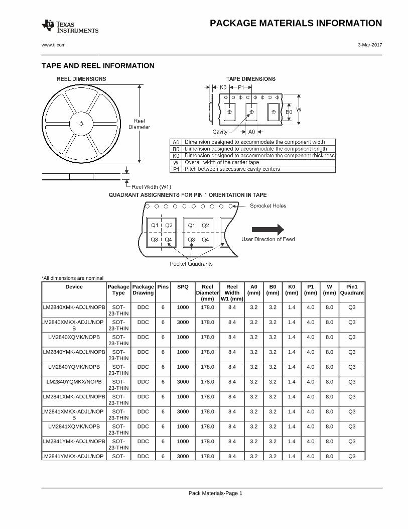
TAPE AND REEL INFORMATION
*All dimensions are nominal
Device PackageType
PackageDrawing
Pins SPQ ReelDiameter
(mm)
ReelWidth
W1 (mm)
A0(mm)
B0(mm)
K0(mm)
P1(mm)
W(mm)
Pin1Quadrant
LM2840XMK-ADJL/NOPB SOT-23-THIN
DDC 6 1000 178.0 8.4 3.2 3.2 1.4 4.0 8.0 Q3
LM2840XMKX-ADJL/NOPB
SOT-23-THIN
DDC 6 3000 178.0 8.4 3.2 3.2 1.4 4.0 8.0 Q3
LM2840XQMK/NOPB SOT-23-THIN
DDC 6 1000 178.0 8.4 3.2 3.2 1.4 4.0 8.0 Q3
LM2840YMK-ADJL/NOPB SOT-23-THIN
DDC 6 1000 178.0 8.4 3.2 3.2 1.4 4.0 8.0 Q3
LM2840YQMK/NOPB SOT-23-THIN
DDC 6 1000 178.0 8.4 3.2 3.2 1.4 4.0 8.0 Q3
LM2840YQMKX/NOPB SOT-23-THIN
DDC 6 3000 178.0 8.4 3.2 3.2 1.4 4.0 8.0 Q3
LM2841XMK-ADJL/NOPB SOT-23-THIN
DDC 6 1000 178.0 8.4 3.2 3.2 1.4 4.0 8.0 Q3
LM2841XMKX-ADJL/NOPB
SOT-23-THIN
DDC 6 3000 178.0 8.4 3.2 3.2 1.4 4.0 8.0 Q3
LM2841XQMK/NOPB SOT-23-THIN
DDC 6 1000 178.0 8.4 3.2 3.2 1.4 4.0 8.0 Q3
LM2841YMK-ADJL/NOPB SOT-23-THIN
DDC 6 1000 178.0 8.4 3.2 3.2 1.4 4.0 8.0 Q3
LM2841YMKX-ADJL/NOP SOT- DDC 6 3000 178.0 8.4 3.2 3.2 1.4 4.0 8.0 Q3
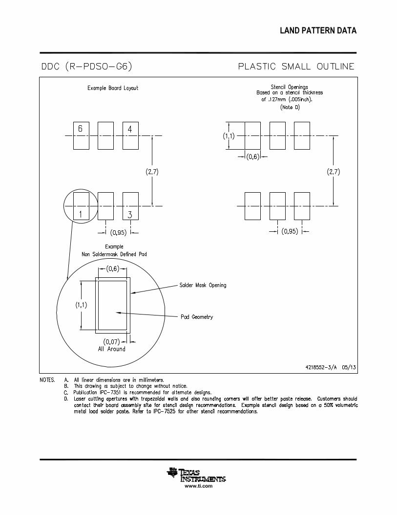
PACKAGE MATERIALS INFORMATION
www.ti.com 3-Mar-2017
Pack Materials-Page 1

Device PackageType
PackageDrawing
Pins SPQ ReelDiameter
(mm)
ReelWidth
W1 (mm)
A0(mm)
B0(mm)
K0(mm)
P1(mm)
W(mm)
Pin1Quadrant
B 23-THIN
LM2841YQMK/NOPB SOT-23-THIN
DDC 6 1000 178.0 8.4 3.2 3.2 1.4 4.0 8.0 Q3
LM2841YQMKX/NOPB SOT-23-THIN
DDC 6 3000 178.0 8.4 3.2 3.2 1.4 4.0 8.0 Q3
LM2842XMK-ADJL/NOPB SOT-23-THIN
DDC 6 1000 178.0 8.4 3.2 3.2 1.4 4.0 8.0 Q3
LM2842XMKX-ADJL/NOPB
SOT-23-THIN
DDC 6 3000 178.0 8.4 3.2 3.2 1.4 4.0 8.0 Q3
LM2842XQMK/NOPB SOT-23-THIN
DDC 6 1000 178.0 8.4 3.2 3.2 1.4 4.0 8.0 Q3
LM2842XQMKX/NOPB SOT-23-THIN
DDC 6 3000 178.0 8.4 3.2 3.2 1.4 4.0 8.0 Q3
LM2842YMK-ADJL/NOPB SOT-23-THIN
DDC 6 1000 178.0 8.4 3.2 3.2 1.4 4.0 8.0 Q3
LM2842YMKX-ADJL/NOPB
SOT-23-THIN
DDC 6 3000 178.0 8.4 3.2 3.2 1.4 4.0 8.0 Q3
LM2842YQMK/NOPB SOT-23-THIN
DDC 6 1000 178.0 8.4 3.2 3.2 1.4 4.0 8.0 Q3
LM2842YQMKX/NOPB SOT-23-THIN
DDC 6 3000 178.0 8.4 3.2 3.2 1.4 4.0 8.0 Q3
*All dimensions are nominal
PACKAGE MATERIALS INFORMATION
www.ti.com 3-Mar-2017
Pack Materials-Page 2

Device Package Type Package Drawing Pins SPQ Length (mm) Width (mm) Height (mm)
LM2840XMK-ADJL/NOPB SOT-23-THIN DDC 6 1000 210.0 185.0 35.0
LM2840XMKX-ADJL/NOPB
SOT-23-THIN DDC 6 3000 210.0 185.0 35.0
LM2840XQMK/NOPB SOT-23-THIN DDC 6 1000 210.0 185.0 35.0
LM2840YMK-ADJL/NOPB SOT-23-THIN DDC 6 1000 210.0 185.0 35.0
LM2840YQMK/NOPB SOT-23-THIN DDC 6 1000 210.0 185.0 35.0
LM2840YQMKX/NOPB SOT-23-THIN DDC 6 3000 210.0 185.0 35.0
LM2841XMK-ADJL/NOPB SOT-23-THIN DDC 6 1000 210.0 185.0 35.0
LM2841XMKX-ADJL/NOPB
SOT-23-THIN DDC 6 3000 210.0 185.0 35.0
LM2841XQMK/NOPB SOT-23-THIN DDC 6 1000 210.0 185.0 35.0
LM2841YMK-ADJL/NOPB SOT-23-THIN DDC 6 1000 210.0 185.0 35.0
LM2841YMKX-ADJL/NOPB
SOT-23-THIN DDC 6 3000 210.0 185.0 35.0
LM2841YQMK/NOPB SOT-23-THIN DDC 6 1000 210.0 185.0 35.0
LM2841YQMKX/NOPB SOT-23-THIN DDC 6 3000 210.0 185.0 35.0
LM2842XMK-ADJL/NOPB SOT-23-THIN DDC 6 1000 210.0 185.0 35.0
LM2842XMKX-ADJL/NOPB
SOT-23-THIN DDC 6 3000 210.0 185.0 35.0
LM2842XQMK/NOPB SOT-23-THIN DDC 6 1000 210.0 185.0 35.0
LM2842XQMKX/NOPB SOT-23-THIN DDC 6 3000 210.0 185.0 35.0
LM2842YMK-ADJL/NOPB SOT-23-THIN DDC 6 1000 210.0 185.0 35.0
LM2842YMKX-ADJL/NOPB
SOT-23-THIN DDC 6 3000 210.0 185.0 35.0
LM2842YQMK/NOPB SOT-23-THIN DDC 6 1000 210.0 185.0 35.0
LM2842YQMKX/NOPB SOT-23-THIN DDC 6 3000 210.0 185.0 35.0
PACKAGE MATERIALS INFORMATION
www.ti.com 3-Mar-2017
Pack Materials-Page 3


IMPORTANT NOTICE
Texas Instruments Incorporated (TI) reserves the right to make corrections, enhancements, improvements and other changes to itssemiconductor products and services per JESD46, latest issue, and to discontinue any product or service per JESD48, latest issue. Buyersshould obtain the latest relevant information before placing orders and should verify that such information is current and complete.TI’s published terms of sale for semiconductor products (http://www.ti.com/sc/docs/stdterms.htm) apply to the sale of packaged integratedcircuit products that TI has qualified and released to market. Additional terms may apply to the use or sale of other types of TI products andservices.Reproduction of significant portions of TI information in TI data sheets is permissible only if reproduction is without alteration and isaccompanied by all associated warranties, conditions, limitations, and notices. TI is not responsible or liable for such reproduceddocumentation. Information of third parties may be subject to additional restrictions. Resale of TI products or services with statementsdifferent from or beyond the parameters stated by TI for that product or service voids all express and any implied warranties for theassociated TI product or service and is an unfair and deceptive business practice. TI is not responsible or liable for any such statements.Buyers and others who are developing systems that incorporate TI products (collectively, “Designers”) understand and agree that Designersremain responsible for using their independent analysis, evaluation and judgment in designing their applications and that Designers havefull and exclusive responsibility to assure the safety of Designers' applications and compliance of their applications (and of all TI productsused in or for Designers’ applications) with all applicable regulations, laws and other applicable requirements. Designer represents that, withrespect to their applications, Designer has all the necessary expertise to create and implement safeguards that (1) anticipate dangerousconsequences of failures, (2) monitor failures and their consequences, and (3) lessen the likelihood of failures that might cause harm andtake appropriate actions. Designer agrees that prior to using or distributing any applications that include TI products, Designer willthoroughly test such applications and the functionality of such TI products as used in such applications.TI’s provision of technical, application or other design advice, quality characterization, reliability data or other services or information,including, but not limited to, reference designs and materials relating to evaluation modules, (collectively, “TI Resources”) are intended toassist designers who are developing applications that incorporate TI products; by downloading, accessing or using TI Resources in anyway, Designer (individually or, if Designer is acting on behalf of a company, Designer’s company) agrees to use any particular TI Resourcesolely for this purpose and subject to the terms of this Notice.TI’s provision of TI Resources does not expand or otherwise alter TI’s applicable published warranties or warranty disclaimers for TIproducts, and no additional obligations or liabilities arise from TI providing such TI Resources. TI reserves the right to make corrections,enhancements, improvements and other changes to its TI Resources. TI has not conducted any testing other than that specificallydescribed in the published documentation for a particular TI Resource.Designer is authorized to use, copy and modify any individual TI Resource only in connection with the development of applications thatinclude the TI product(s) identified in such TI Resource. NO OTHER LICENSE, EXPRESS OR IMPLIED, BY ESTOPPEL OR OTHERWISETO ANY OTHER TI INTELLECTUAL PROPERTY RIGHT, AND NO LICENSE TO ANY TECHNOLOGY OR INTELLECTUAL PROPERTYRIGHT OF TI OR ANY THIRD PARTY IS GRANTED HEREIN, including but not limited to any patent right, copyright, mask work right, orother intellectual property right relating to any combination, machine, or process in which TI products or services are used. Informationregarding or referencing third-party products or services does not constitute a license to use such products or services, or a warranty orendorsement thereof. Use of TI Resources may require a license from a third party under the patents or other intellectual property of thethird party, or a license from TI under the patents or other intellectual property of TI.TI RESOURCES ARE PROVIDED “AS IS” AND WITH ALL FAULTS. TI DISCLAIMS ALL OTHER WARRANTIES ORREPRESENTATIONS, EXPRESS OR IMPLIED, REGARDING RESOURCES OR USE THEREOF, INCLUDING BUT NOT LIMITED TOACCURACY OR COMPLETENESS, TITLE, ANY EPIDEMIC FAILURE WARRANTY AND ANY IMPLIED WARRANTIES OFMERCHANTABILITY, FITNESS FOR A PARTICULAR PURPOSE, AND NON-INFRINGEMENT OF ANY THIRD PARTY INTELLECTUALPROPERTY RIGHTS. TI SHALL NOT BE LIABLE FOR AND SHALL NOT DEFEND OR INDEMNIFY DESIGNER AGAINST ANY CLAIM,INCLUDING BUT NOT LIMITED TO ANY INFRINGEMENT CLAIM THAT RELATES TO OR IS BASED ON ANY COMBINATION OFPRODUCTS EVEN IF DESCRIBED IN TI RESOURCES OR OTHERWISE. IN NO EVENT SHALL TI BE LIABLE FOR ANY ACTUAL,DIRECT, SPECIAL, COLLATERAL, INDIRECT, PUNITIVE, INCIDENTAL, CONSEQUENTIAL OR EXEMPLARY DAMAGES INCONNECTION WITH OR ARISING OUT OF TI RESOURCES OR USE THEREOF, AND REGARDLESS OF WHETHER TI HAS BEENADVISED OF THE POSSIBILITY OF SUCH DAMAGES.Unless TI has explicitly designated an individual product as meeting the requirements of a particular industry standard (e.g., ISO/TS 16949and ISO 26262), TI is not responsible for any failure to meet such industry standard requirements.Where TI specifically promotes products as facilitating functional safety or as compliant with industry functional safety standards, suchproducts are intended to help enable customers to design and create their own applications that meet applicable functional safety standardsand requirements. Using products in an application does not by itself establish any safety features in the application. Designers mustensure compliance with safety-related requirements and standards applicable to their applications. Designer may not use any TI products inlife-critical medical equipment unless authorized officers of the parties have executed a special contract specifically governing such use.Life-critical medical equipment is medical equipment where failure of such equipment would cause serious bodily injury or death (e.g., lifesupport, pacemakers, defibrillators, heart pumps, neurostimulators, and implantables). Such equipment includes, without limitation, allmedical devices identified by the U.S. Food and Drug Administration as Class III devices and equivalent classifications outside the U.S.TI may expressly designate certain products as completing a particular qualification (e.g., Q100, Military Grade, or Enhanced Product).Designers agree that it has the necessary expertise to select the product with the appropriate qualification designation for their applicationsand that proper product selection is at Designers’ own risk. Designers are solely responsible for compliance with all legal and regulatoryrequirements in connection with such selection.Designer will fully indemnify TI and its representatives against any damages, costs, losses, and/or liabilities arising out of Designer’s non-compliance with the terms and provisions of this Notice.
Mailing Address: Texas Instruments, Post Office Box 655303, Dallas, Texas 75265Copyright © 2017, Texas Instruments Incorporated