lm26420 dual 2-a, high-efficiency synchronous dc/dc converter · 2018-05-22 · • local 5 v to...
TRANSCRIPT

VIN
PG1 PG2
SW1 SW2
FB1 FB2
GND
LM26
420VOUT1
2.5 V/2 A
VIN
3 V to 5.5 V
EN1 EN2
Buck 1 Buck 2VOUT2
1.2 V/2 A
Copyright © 2016, Texas Instruments Incorporated
Product
Folder
Order
Now
Technical
Documents
Tools &
Software
Support &Community
ReferenceDesign
An IMPORTANT NOTICE at the end of this data sheet addresses availability, warranty, changes, use in safety-critical applications,intellectual property matters and other important disclaimers. PRODUCTION DATA.
LM26420SNVS579L –FEBRUARY 2009–REVISED MAY 2018
LM26420 Dual 2-A, High-Efficiency SynchronousDC/DC Converter
1
1 Features1• Compliant with CISPR25 Class 5 Conducted
Emissions• Input Voltage Range of 3 V to 5.5 V• Output Voltage Range of 0.8 V to 4.5 V• 2-A Output Current per Regulator• High Switching Frequency: 2.2 MHz (LM26420X)
0.55 MHz (LM26420Y)• 0.8 V, 1.5% Internal Voltage Reference• Internal Soft Start• Independent Power Good and Precision Enable
for Each Output• Current Mode, PWM Operation• Thermal Shutdown• Overvoltage Protection• Start-up into Prebiased Output Loads• Regulators are 180° Out of Phase• Create a Custom Design Using the LM26420 With
the WEBENCH® Power Designer
2 Applications• Local 5 V to Vcore of FPGAs• Core Power in HDDs and Set-Top Boxes• USB Powered Devices• Powering Core and I/O Voltages for CPUs and
ASICsspace
3 DescriptionThe LM26420 regulator is a monolithic, high-efficiency dual PWM step-down DC/DC converter.This device has the ability to drive two 2-A loads withan internal 75-mΩ PMOS top switch and an internal50-mΩ NMOS bottom switch using state-of-the-artBICMOS technology results in the best power densityavailable. The world-class control circuitry allow ontimes as low as 30 ns, thus supporting exceptionallyhigh-frequency conversion over the entire 3-V to 5.5-V input operating range down to the minimum outputvoltage of 0.8 V.
Although the operating frequency is high, efficienciesup to 93% are easy to achieve. External shutdown isincluded, featuring an ultra-low standby current. TheLM26420 utilizes current-mode control and internalcompensation to provide high performance regulationover a wide range of operating conditions.
Device Information(1)
PART NUMBER PACKAGE BODY SIZE (NOM)
LM26420HTSSOP (20) 6.50 mm × 4.40 mmWQFN (16) 4.00 mm × 4.00 mm
(1) For all available packages, see the orderable addendum atthe end of the data sheet.
LM26420 Dual Buck DC/DC ConverterLM26420 Efficiency (Up to 93%)
2
LM26420SNVS579L –FEBRUARY 2009–REVISED MAY 2018 www.ti.com
Product Folder Links: LM26420
Submit Documentation Feedback Copyright © 2009–2018, Texas Instruments Incorporated
Table of Contents1 Features .................................................................. 12 Applications ........................................................... 13 Description ............................................................. 14 Revision History..................................................... 25 Pin Configuration and Functions ......................... 46 Specifications......................................................... 6
6.1 Absolute Maximum Ratings ...................................... 66.2 ESD Ratings (LM26420X/Y) .................................... 66.3 Recommended Operating Conditions....................... 66.4 Thermal Information .................................................. 66.5 Electrical Characteristics Per Buck ........................... 76.6 Typical Characteristics .............................................. 8
7 Detailed Description ............................................ 137.1 Overview ................................................................. 137.2 Functional Block Diagram ....................................... 147.3 Feature Description................................................. 147.4 Device Functional Modes........................................ 15
8 Application and Implementation ........................ 168.1 Application Information............................................ 168.2 Typical Applications ............................................... 19
9 Power Supply Recommendations ...................... 3210 Layout................................................................... 32
10.1 Layout Guidelines ................................................. 3210.2 Layout Example .................................................... 3310.3 Thermal Considerations ........................................ 33
11 Device and Documentation Support ................. 3611.1 Device Support...................................................... 3611.2 Documentation Support ........................................ 3611.3 Receiving Notification of Documentation Updates 3611.4 Community Resources.......................................... 3611.5 Trademarks ........................................................... 3611.6 Electrostatic Discharge Caution............................ 3711.7 Glossary ................................................................ 37
12 Mechanical, Packaging, and OrderableInformation ........................................................... 37
4 Revision History
Changes from Revision K (April 2016) to Revision L Page
• Split automotive data sheet to separate document (SNVSB35) and remove automotive-specific content fromSNVS579 ............................................................................................................................................................................... 1
• Added links for WEBENCH .................................................................................................................................................... 1
Changes from Revision J (September 2015) to Revision K Page
• Changed RθJA value from 35°C/W to 38.5°C/W for PWP package and from 40°C/W to 36.2°C/W; replaced RθJCvalues with 2 new rows (and new values); added additional thermal values......................................................................... 6
• Changed "C1" to "C2" on Figure 42 ..................................................................................................................................... 20• Changed "C1" to "C2" on Figure 51 ..................................................................................................................................... 29• Deleted "C7" and "C8" from Table 6 ................................................................................................................................... 30
Changes from Revision I (June 2015) to Revision J Page
• fixed error in WQFN Pin Functions - shifted "Description" column down one row and added back description forVIND1 pin ................................................................................................................................................................................ 4
• Changed reference from "Typical Applications" to "Table 1". ............................................................................................. 22• Deleted definition for RDS (not part of equation 15) ............................................................................................................. 22
Changes from Revision H (August 2014) to Revision I Page
• Changed "Frequency" to "Efficiency" in title; add new Feature bullet re: CISPR25............................................................... 1• Changed moved Storage temperature to Absolute Maximum Ratings table ......................................................................... 6• Changed figure 36 caption .................................................................................................................................................. 13• Added part number to caption wording ................................................................................................................................ 14• Added application note ........................................................................................................................................................ 16• Changed title of Thermal Guidelines to Thermal Considerations and moved the section to the correct location................ 33

3
LM26420www.ti.com SNVS579L –FEBRUARY 2009–REVISED MAY 2018
Product Folder Links: LM26420
Submit Documentation FeedbackCopyright © 2009–2018, Texas Instruments Incorporated
• Added Related Documentation and Community Resources subsections ............................................................................ 36
Changes from Revision G (July 2014) to Revision H Page
• Changed percent sign to suffix .............................................................................................................................................. 7
Changes from Revision F (March 2013) to Revision G Page
• Changed formatting to match new TI datasheet guidelines; added Device Information and Handling Ratings tables,Layout, and Device and Documentation Support sections; reformatted Functional Description to DetailedDescription and Applications to Applications and Implementation sections........................................................................... 1
• Changed to new equation..................................................................................................................................................... 34

1
16
2 3 4 5 6 7 8
15 14 13 1112
9 10
20 19 18 17
5
6
7
4 3 2 1
16
15
14
13
9 10 11 12
8
DAP
4
LM26420SNVS579L –FEBRUARY 2009–REVISED MAY 2018 www.ti.com
Product Folder Links: LM26420
Submit Documentation Feedback Copyright © 2009–2018, Texas Instruments Incorporated
5 Pin Configuration and Functions
RUM Package16-Pin WQFN
Top ViewPWP Package
20-Pin HTSSOPTop View
Pin Functions: 16-Pin WQFNPIN
TYPE DESCRIPTIONNUMBER NAME1,2 VIND1 P Power input supply for Buck 1.3 SW1 P Output switch for Buck 1. Connect to the inductor.4 PGND1 G Power ground pin for Buck 1.5 FB1 A Feedback pin for Buck 1. Connect to external resistor divider to set output voltage.6 PG1 G Power Good Indicator for Buck 1. Pin is connected through a resistor to an external supply
(open drain output).7 PG2 G Power Good Indicator for Buck 2. Pin is connected through a resistor to an external supply
(open drain output).8 FB2 A Feedback pin for Buck 2. Connect to external resistor divider to set output voltage.9 PGND2 G Power ground pin for Buck 2.10 SW2 P Output switch for Buck 2. Connect to the inductor.11, 12 VIND2 A Power Input supply for Buck 2.13 EN2 A Enable control input. Logic high enable operation for Buck 2. Do not allow this pin to float or
be greater than VIN + 0.3 V.14 AGND G Signal ground pin. Place the bottom resistor of the feedback network as close as possible to
pin.15 VINC A Input supply for control circuitry.16 EN1 A Enable control input. Logic high enable operation for Buck 1. Do not allow this pin to float or
be greater than VIN + 0.3 V.DAP Die Attach Pad — Connect to system ground for low thermal impedance and as a primary electrical GND
connection.

5
LM26420www.ti.com SNVS579L –FEBRUARY 2009–REVISED MAY 2018
Product Folder Links: LM26420
Submit Documentation FeedbackCopyright © 2009–2018, Texas Instruments Incorporated
Pin Functions 20-Pin HTSSOPPIN
TYPE DESCRIPTIONNUMBER NAME1 VINC A Input supply for control circuitry.2 EN1 A Enable control input. Logic high enable operation for Buck 1. Do not allow this pin to float or
be greater than VIN + 0.3 V.3, 4 VIND1 A Power Input supply for Buck 1.5 SW1 P Output switch for Buck 1. Connect to the inductor.6,7 PGND1 G Power ground pin for Buck 1.8 FB1 A Feedback pin for Buck 1. Connect to external resistor divider to set output voltage.9 PG1 G Power Good Indicator for Buck 1. Pin is connected through a resistor to an external supply
(open drain output).10, 11, DAP Die Attach Pad — Connect to system ground for low thermal impedance, but it cannot be used as a primary
GND connection.12 PG2 G Power Good Indicator for Buck 2. Pin is connected through a resistor to an external supply
(open drain output).13 FB2 A Feedback pin for Buck 2. Connect to external resistor divider to set output voltage.14, 15 PGND2 G Power ground pin for Buck 2.16 SW2 P Output switch for Buck 2. Connect to the inductor.17, 18 VIND2 A Power Input supply for Buck 2.19 EN2 A Enable control input. Logic high enable operation for Buck 2. Do not allow this pin to float or
be greater than VIN + 0.3 V.20 AGND G Signal ground pin. Place the bottom resistor of the feedback network as close as possible to
pin.

6
LM26420SNVS579L –FEBRUARY 2009–REVISED MAY 2018 www.ti.com
Product Folder Links: LM26420
Submit Documentation Feedback Copyright © 2009–2018, Texas Instruments Incorporated
(1) Stresses beyond those listed under Absolute Maximum Ratings may cause permanent damage to the device. These are stress ratingsonly, which do not imply functional operation of the device at these or any other conditions beyond those indicated under RecommendedOperating Conditions. Exposure to absolute-maximum-rated conditions for extended periods may affect device reliability.
6 Specifications
6.1 Absolute Maximum RatingsOver operating free-air temperature range (unless otherwise noted) (1)
MIN MAX UNIT
Input voltagesVIN –0.5 7
VFB –0.5 3EN –0.5 7
Output voltages SW –0.5 7 VInfrared or convection reflow (15 sec) Soldering Information 220 °CStorage temperature Tstg –65 150 °C
(1) JEDEC document JEP155 states that 500-V HBM allows safe manufacturing with a standard ESD control process.(2) JEDEC document JEP157 states that 250-V CDM allows safe manufacturing with a standard ESD control process.
6.2 ESD Ratings (LM26420X/Y)VALUE UNIT
V(ESD) Electrostatic dischargeHuman-body model (HBM), per ANSI/ESDA/JEDEC JS-001 (1) ±2000
VCharged-device model (CDM), per JEDEC specification JESD22-C101 (2) ±750
6.3 Recommended Operating ConditionsOver operating free-air temperature range (unless otherwise noted)
MIN MAX UNITVIN 3 5.5 VJunction temperature (Q1) –40 125
°CJunction temperature (Q0) –40 150
(1) For more information about traditional and new thermal metrics, see the Semiconductor and IC Package Thermal Metrics applicationreport.
6.4 Thermal Information
THERMAL METRIC (1)LM26420
UNITPWP (HTSSOP) RUM (WQFN)20 PINS 16 PINS
RθJA Junction-to-ambient thermal resistance 38.5 36.2 °C/WRθJC(top) Junction-to-case thermal resistance 21.0 32.7 °C/WRθJB Junction-to-board thermal resistance 19.9 14.1 °C/WψJT Junction-to-top characterization parameter 0.7 0.3 °C/WψJB Junction-to-board characterization parameter 19.7 14.2 °C/WRθJC(bot) Junction-to-case (bottom) thermal resistance 3.5 4.1 °C/W

7
LM26420www.ti.com SNVS579L –FEBRUARY 2009–REVISED MAY 2018
Product Folder Links: LM26420
Submit Documentation FeedbackCopyright © 2009–2018, Texas Instruments Incorporated
6.5 Electrical Characteristics Per BuckOver operating free-air temperature range (unless otherwise noted)
PARAMETER TEST CONDITIONS MIN TYP MAX UNITVFB Feedback Voltage 0.788 0.8 0.812 VΔVFB/VIN Feedback Voltage Line Regulation VIN = 3 V to 5.5 V 0.05 %/VIB Feedback Input Bias Current 0.4 100 nA
UVLOUndervoltage Lockout
VIN Rising 2.628 2.9 VVIN Falling 2 2.3 V
UVLO Hysteresis 330 mVFSW Switching Frequency LM26420-X 1.85 2.2 2.65 MHzFSW Switching Frequency LM26420-Y 0.4 0.55 0.7FFB Frequency Foldback LM26420-X 300 kHzFFB Frequency Foldback LM26420-Y 150DMAX Maximum Duty Cycle LM26420-X 86% 91.5%DMAX Maximum Duty Cycle LM26420-Y 90% 98%
RDSON_TOP TOP Switch On ResistanceWQFN-16 Package 75 135
mΩHTSSOP-20 Package 70 135
RDSON_BOT BOTTOM Switch On ResistanceWQFN-16 Package 55 100
mΩTSSOP-20 Package 45 80
ICL_TOP TOP Switch Current Limit VIN = 3.3 V 2.4 3.3 AICL_BOT BOTTOM Switch Reverse Current
LimitVIN = 3.3 V 0.4 0.75 A
ΔΦ Phase Shift Between SW1 and SW2 160 180 200 °
VEN_THEnable Threshold Voltage 0.97 1.04 1.12
VEnable Threshold Hysteresis 0.15
ISW_TOP Switch Leakage –0.7 µAIEN Enable Pin Current Sink/Source 5 nAVPG-TH-U Upper Power Good Threshold FB Pin Voltage Rising 848 925 1,008 mV
Upper Power Good Hysteresis 40 mVVPG-TH-L Lower Power Good Threshold FB Pin Voltage Rising 656 710 791 mV
Lower Power Good Hysteresis 40 mV
IQVINC
VINC Quiescent Current (non-switching) with both outputs on
LM26420X/Y VFB = 0.9 V 3.3 5
mAVINC Quiescent Current (switching)with both outputs on
LM26420X/Y VFB = 0.7 V 4.7 6.2
VINC Quiescent Current (shutdown) All Options VEN = 0 V 0.05 µA
IQVIND
VIND Quiescent Current (non-switching)
LM26420X/Y VFB = 0.9 V 0.9 1.5mA
VIND Quiescent Current (switching) LM26420X VFB = 0.7 V 11 15IQVIND VIND Quiescent Current (switching) LM26420Y VFB = 0.7 V 3.7 7.5 mAIQVIND VIND Quiescent Current (shutdown) All Options VEN = 0 V 0.1 µATSD Thermal Shutdown Temperature 165 °C

8
LM26420SNVS579L –FEBRUARY 2009–REVISED MAY 2018 www.ti.com
Product Folder Links: LM26420
Submit Documentation Feedback Copyright © 2009–2018, Texas Instruments Incorporated
6.6 Typical CharacteristicsAll curves taken at VIN = 5 V with configuration in typical application circuits shown in Application and Implementation. TJ =25°C, unless otherwise specified.
Figure 1. Efficiency vs Load, X Option Figure 2. Efficiency Vs Load, Y Option
Figure 3. Efficiency vs Load, X Option Figure 4. Efficiency vs Load, Y Option
Figure 5. Efficiency vs Load, X Option Figure 6. Efficiency vs Load, Y Option

LOAD (A)
OU
TP
UT
(V)
1.808
1.807
1.806
1.805
1.804
1.803
1.802
1.8010.0 0.25 0.5 0.75 1.0 1.25 1.5 1.75 2.0
LOAD (A)
OU
TP
UT
(V)
1.808
1.807
1.806
1.805
1.804
1.803
1.802
1.8010.0 0.25 0.5 0.75 1.0 1.25 1.5 1.75 2.0
9
LM26420www.ti.com SNVS579L –FEBRUARY 2009–REVISED MAY 2018
Product Folder Links: LM26420
Submit Documentation FeedbackCopyright © 2009–2018, Texas Instruments Incorporated
Typical Characteristics (continued)All curves taken at VIN = 5 V with configuration in typical application circuits shown in Application and Implementation. TJ =25°C, unless otherwise specified.
Figure 7. Efficiency vs Load, X Option Figure 8. Efficiency vs Load, Y Option
Figure 9. Efficiency vs Load, X Option Figure 10. Efficiency vs Load, Y Option
VIN = 5 V VOUT = 1.8 V
Figure 11. Load Regulation (All Options)
VIN = 3 V VOUT = 1.8 V
Figure 12. Load Regulation (All Options)

TEMPERATURE (°C)
WQ
FN
-T
OP
FE
T-
RD
SO
N(m
)Ω
110
100
90
80
70
60
50-50 -25 0 25 50 75 100 125
TEMPERATURE (°C)
WQ
FN
- B
OT
TO
M F
ET
- R
DS
ON
(m)
Ω
80
70
60
50
40
30-50 -25 0 25 50 75 100 125
INPUT VOLTAGE (V)
OU
TP
UT
(V)
1.808
1.807
1.806
1.805
1.804
1.803
1.8023.0 3.5 4.0 4.5 5.0 5.5
INPUT VOLTAGE (V)
OU
TP
UT
(V)
1.798
1.797
1.796
1.795
1.794
1.793
1.7923.0 3.5 4.0 4.5 5.0 5.5
10
LM26420SNVS579L –FEBRUARY 2009–REVISED MAY 2018 www.ti.com
Product Folder Links: LM26420
Submit Documentation Feedback Copyright © 2009–2018, Texas Instruments Incorporated
Typical Characteristics (continued)All curves taken at VIN = 5 V with configuration in typical application circuits shown in Application and Implementation. TJ =25°C, unless otherwise specified.
VOUT = 1.8 V IOUT = 1000 mA
Figure 13. Line Regulation, X Option
VOUT = 1.8 V IOUT = 1000 mA
Figure 14. Line Regulation - Y Option
Figure 15. Oscillator Frequency vs Temperature,, X Option Figure 16. Oscillator Frequency vs Temperature, Y Option
Figure 17. RDSON Top Vs Temperature (WQFN-16 Package) Figure 18. RDSON Bottom Vs Temperature(WQFN-16 Package)

TEMPERATURE (°C)
CU
RR
EN
TLIM
IT(A
)
3.50
3.45
3.40
3.35
3.30
3.25
3.20
3.15
3.10-50 -25 0 25 50 75 100 125
TEMPERATURE (°C)
I QS
WIT
CH
ING
-V
IND
(mA
)
3.9
3.8
3.7
3.6
3.5
3.4-50 -25 0 25 50 75 100 125
Y Version
TEMPERATURE (°C)
I QS
WIT
CH
ING
-V
IND
(mA
)
11.6
11.4
11.2
11.0
10.8
10.6-50 -25 0 25 50 75 100 125
X Version
TEMPERATURE (°C)
TS
SO
P-
TO
PF
ET
- R
DS
ON
(m)
Ω
110
100
90
80
70
60
50-50 -25 0 25 50 75 100 125
TEMPERATURE (°C)
TS
SO
P-
BO
TT
OM
FE
T-
RD
SO
N(m
)Ω
80
70
60
50
40
30
20-50 -25 0 25 50 75 100 125
11
LM26420www.ti.com SNVS579L –FEBRUARY 2009–REVISED MAY 2018
Product Folder Links: LM26420
Submit Documentation FeedbackCopyright © 2009–2018, Texas Instruments Incorporated
Typical Characteristics (continued)All curves taken at VIN = 5 V with configuration in typical application circuits shown in Application and Implementation. TJ =25°C, unless otherwise specified.
Figure 19. RDSON Top Vs Temperature (TSSOP-20 Package) Figure 20. RDSON Bottom vs Temperature(TSSOP-20 Package)
Figure 21. IQ (Quiescent Current Switching), X Option Figure 22. IQ (Quiescent Current Switching), Y Option
Figure 23. VFB vs Temperature
VIN = 5 V and 3.3 V
Figure 24. Current Limit vs Temperature

TEMPERATURE (°C)
RE
VE
RS
EC
UR
RE
NT
LIM
IT(A
)
0.78
0.77
0.76
0.75
0.74
0.73
0.72
0.71
0.70-50 -25 0 25 50 75 100 125
12
LM26420SNVS579L –FEBRUARY 2009–REVISED MAY 2018 www.ti.com
Product Folder Links: LM26420
Submit Documentation Feedback Copyright © 2009–2018, Texas Instruments Incorporated
Typical Characteristics (continued)All curves taken at VIN = 5 V with configuration in typical application circuits shown in Application and Implementation. TJ =25°C, unless otherwise specified.
Figure 25. Reverse Current Limit vs Temperature Figure 26. Short Circuit Waveforms

0
0
VIN
TON
t
t
InductorCurrent
D = TON/TSW
VSW
TOFF
TSWIL
IPK
SWVoltage
13
LM26420www.ti.com SNVS579L –FEBRUARY 2009–REVISED MAY 2018
Product Folder Links: LM26420
Submit Documentation FeedbackCopyright © 2009–2018, Texas Instruments Incorporated
7 Detailed Description
7.1 OverviewThe LM26420 is a constant frequency dual PWM buck synchronous regulator device that can supply two loads atup to 2 A each. The regulator has a preset switching frequency of either 2.2 MHz or 550 kHz. This highfrequency allows the LM26420 to operate with small surface mount capacitors and inductors, resulting in aDC/DC converter that requires a minimum amount of board space. The LM26420 is internally compensated, so itis simple to use and requires few external components. The LM26420 uses current-mode control to regulate theoutput voltage. The following operating description of the LM26420 refers to the Functional Block Diagram, whichdepicts the functional blocks for one of the two channels, and to the waveforms in Figure 27. The LM26420supplies a regulated output voltage by switching the internal PMOS and NMOS switches at constant frequencyand variable duty cycle. A switching cycle begins at the falling edge of the reset pulse generated by the internalclock. When this pulse goes low, the output control logic turns on the internal PMOS control switch (TOP Switch).During this on-time, the SW pin voltage (VSW) swings up to approximately VIN, and the inductor current (IL)increases with a linear slope. IL is measured by the current sense amplifier, which generates an outputproportional to the switch current. The sense signal is summed with the regulator’s corrective ramp andcompared to the error amplifier’s output, which is proportional to the difference between the feedback voltageand VREF. When the PWM comparator output goes high, the TOP Switch turns off and the NMOS switch(BOTTOM Switch) turns on after a short delay, which is controlled by the Dead-Time-Control Logic, until the nextswitching cycle begins. During the top switch off-time, inductor current discharges through the BOTTOM Switch,which forces the SW pin to swing to ground. The regulator loop adjusts the duty cycle (D) to maintain a constantoutput voltage.
Figure 27. LM26420 Basic Operation of the PWM Comparator

ENABLE and UVLO ThermalSHDN
Internal - LDO
EN
SWFB
GND
VIN
Dead-Time-
Control Logic
Pgood
880 mV
720 mV
OVPSHDN
SOFT-START
Internal-Comp
DRIVERS
Control Logic
ISENSE
ILIMIT
P-FET
N-FET
VREF=0.8 V +-
2.2 MHz/550 kHz
+-
+-
+-
+-
+ -VREF+-
x 1.15
S R
R Q
Q
R S
IREVERSE-LIMIT
Clock
+-
+-
RAMPArtificial
ISENSE
Copyright © 2016, Texas Instruments Incorporated
14
LM26420SNVS579L –FEBRUARY 2009–REVISED MAY 2018 www.ti.com
Product Folder Links: LM26420
Submit Documentation Feedback Copyright © 2009–2018, Texas Instruments Incorporated
7.2 Functional Block Diagram
7.3 Feature Description
7.3.1 Soft StartThis function forces VOUT to increase at a controlled rate during start-up in a controlled fashion, which helpsreduce inrush current and eliminate overshoot on VOUT. During soft start, reference voltage of the error amplifierramps from 0 V to its nominal value of 0.8 V in approximately 600 µs. If the converter is turned on into a pre-biased load, then the feedback begins ramping from the prebias voltage but at the same rate as if it had startedfrom 0 V. The two outputs start up ratiometrically if enabled at the same time, see Figure 28 below.

VO
LTA
GE
TIME
RATIOMETRIC START UP
VOUT1
VOUT2
VEN1,2
15
LM26420www.ti.com SNVS579L –FEBRUARY 2009–REVISED MAY 2018
Product Folder Links: LM26420
Submit Documentation FeedbackCopyright © 2009–2018, Texas Instruments Incorporated
Feature Description (continued)
Figure 28. LM26420 Soft-Start
7.3.2 Power GoodThe LM26420 features an open drain power good (PG) pin to sequence external supplies or loads and to providefault detection. This pin requires an external resistor (RPG) to pull PG high when the output is within the PGtolerance window. Typical values for this resistor range from 10 kΩ to 100 kΩ.
7.3.3 Precision EnableThe LM26420 features independent precision enables that allow the converter to be controlled by an externalsignal. This feature allows the device to be sequenced either by a external control signal or the output of anotherconverter in conjunction with a resistor divider network. It can also be set to turn on at a specific input voltagewhen used in conjunction with a resistor divider network connected to the input voltage. The device is enabledwhen the EN pin exceeds 1.04 V and has a 150-mV hysteresis.
7.4 Device Functional Modes
7.4.1 Output Overvoltage ProtectionThe overvoltage comparator compares the FB pin voltage to a voltage that is approximately 15% greater than theinternal reference VREF. Once the FB pin voltage goes 15% above the internal reference, the internal PMOSswitch is turned off, which allows the output voltage to decrease toward regulation.
7.4.2 Undervoltage LockoutUndervoltage lockout (UVLO) prevents the LM26420 from operating until the input voltage exceeds 2.628 V(typical). The UVLO threshold has approximately 330 mV of hysteresis, so the device operates until VIN dropsbelow 2.3 V (typical). Hysteresis prevents the part from turning off during power up if VIN is non-monotonic.
7.4.3 Current LimitThe LM26420 uses cycle-by-cycle current limiting to protect the output switch. During each switching cycle, acurrent limit comparator detects if the output switch current exceeds 3.3 A (typical), and turns off the switch untilthe next switching cycle begins.
7.4.4 Thermal ShutdownThermal shutdown limits total power dissipation by turning off the output switch when the device junctiontemperature exceeds 165°C. After thermal shutdown occurs, the output switch does not turn on until the junctiontemperature drops to approximately 150°C.

V =
1
2.5V0.8V
1 + 2x1
3.5% 1.5%
= 1.4%
V =
1
VOUT
VFB
1 + 2x
1
TOL I
VIND
VINC
EN
AGND PGND
FB
SW
LM26420 VOUTLOUT
COUTR1
R2
Copyright © 2016, Texas Instruments Incorporated
x R2R1 =VREF
VOUT- 1
16
LM26420SNVS579L –FEBRUARY 2009–REVISED MAY 2018 www.ti.com
Product Folder Links: LM26420
Submit Documentation Feedback Copyright © 2009–2018, Texas Instruments Incorporated
8 Application and Implementation
NOTEInformation in the following applications sections is not part of the TI componentspecification, and TI does not warrant its accuracy or completeness. TI’s customers areresponsible for determining suitability of components for their purposes. Customers shouldvalidate and test their design implementation to confirm system functionality.
8.1 Application Information
8.1.1 Programming Output VoltageThe output voltage is set using Equation 1 where R2 is connected between the FB pin and GND, and R1 isconnected between VOUT and the FB pin. A good value for R2 is 10 kΩ. When designing a unity gain converter(VOUT = 0.8 V), R1 must be between 0 Ω and 100 Ω, and R2 must be on the order of 5 kΩ to 50 kΩ. 10 kΩ is thesuggested value where R1 is the top feedback resistor and R2 is the bottom feedback resistor.
(1)VREF = 0.80V (2)
Figure 29. Programming VOUT
To determine the maximum allowed resistor tolerance, use Equation 3:
where• TOL is the set point accuracy of the regulator, is the tolerance of VFB. (3)
Example:
VOUT = 2.5 V, with a setpoint accuracy of ±3.5%.
(4)
Choose 1% resistors. If R2 = 10 kΩ, then R1 is 21.25 kΩ.

VIND1,2
VINC
EN
AGND PGND
FB
SW
LM26420
VIN
CF
RF
CIN
Copyright © 2016, Texas Instruments Incorporated
17
LM26420www.ti.com SNVS579L –FEBRUARY 2009–REVISED MAY 2018
Product Folder Links: LM26420
Submit Documentation FeedbackCopyright © 2009–2018, Texas Instruments Incorporated
Application Information (continued)8.1.2 VINC Filtering ComponentsAdditional filtering is required between VINC and AGND in order to prevent high frequency noise on VIN fromdisturbing the sensitive circuitry connected to VINC. A small RC filter can be used on the VINC pin as shown inFigure 30.
Figure 30. RC Filter On VINC
In general, RF is typically between 1 Ω and 10 Ω so that the steady state voltage drop across the resistor due tothe VINC bias current does not affect the UVLO level. CF can range from 0.22 µF to 1 µF in X7R or X5Rdielectric, where the RC time constant should be at least 2 µs. CF must be placed as close to the device aspossiblewith a direct connection from VINC and AGND.
8.1.3 Using Precision Enable and Power GoodThe LM26420 device precision EN and PG pins address many of the sequencing requirements required intoday's challenging applications. Each output can be controlled independently and have independent powergood. This allows for a multitude of ways to control each output. Typically, the enables to each output are tiedtogether to the input voltage and the outputs ratiometrically ramp up when the input voltage reaches aboveUVLO rising threshold. There may be instances where it is desired that the second output (VOUT2) does not turnon until the first output (VOUT1) has reached 90% of the desired setpoint. This is easily achieved with an externalresistor divider attached from VOUT1 to EN2, see Figure 31.
Figure 31. VOUT1 Controlling VOUT2 with Resistor Divider
If it is not desired to have a resistor divider to control VOUT2 with VOUT1, then the PG1 can be connected to theEN2 pin to control VOUT2, see Figure 32. RPG1 is a pullup resistor on the range of 10 kΩ to 100 kΩ, 50 kΩ is thesuggested value. This turns on VOUT2 when VOUT1 is approximately 90% of the programmed output.
NOTEThis also turns off VOUT2 when VOUT1 is outside the ±10% of the programmed output.

VOUT
t
t
~7.5 Ps
VPG
+14%
-14%-10%
+10%
Copyright © 2016, Texas Instruments Incorporated
VIND
VINC
EN FB
SW
AGND PGND
LM26420
CIN
RF
REN1
REN2
CF
VIN
18
LM26420SNVS579L –FEBRUARY 2009–REVISED MAY 2018 www.ti.com
Product Folder Links: LM26420
Submit Documentation Feedback Copyright © 2009–2018, Texas Instruments Incorporated
Application Information (continued)
Figure 32. PG1 Controlling VOUT2
Another example might be that the output is not to be turned on until the input voltage reaches 90% of desiredvoltage setpoint. This verifies that the input supply is stable before turning on the output. Select REN1 and REN2such that the voltage at the EN pin is greater than 1.12 V when reaching the 90% desired set-point.
Figure 33. VOUT Controlling VIN
The power good feature of the LM26420 is designed with hysteresis in order to ensure no false power good flagsare asserted during large transient. Once power good is asserted high, it is not pulled low until the output voltageexceeds ±14% of the setpoint for a during of approximately 7.5 µs (typical), see Figure 34.
Figure 34. Power Good Hysteresis Operation

VIN1
PG1 PG2
SW1 SW2
FB1 FB2
PGND1, PGND2, AGND, DAP
LM26420
VOUT11.8 V/2 A
VIN3 V to 5.5 V
VOUT20.8 V/2 A
VINc VIN2
EN2EN1
C3 C4
C2 C6C1
L1 L2
C5R7
R6R5
R3
R1 R2
R4
Copyright © 2016, Texas Instruments Incorporated
19
LM26420www.ti.com SNVS579L –FEBRUARY 2009–REVISED MAY 2018
Product Folder Links: LM26420
Submit Documentation FeedbackCopyright © 2009–2018, Texas Instruments Incorporated
Application Information (continued)8.1.4 Overcurrent ProtectionWhen the switch current reaches the current limit value, it is turned off immediately. This effectively reduces theduty cycle and therefore the output voltage dips and continues to droop until the output load matches the peakcurrent limit inductor current. As the FB voltage drops below 480 mV the operating frequency begins to decreaseuntil it hits full on frequency foldback, which is set to approximately 150 kHz for the Y version and 300 kHz for theX version. Frequency foldback helps reduce the thermal stress in the device by reducing the switching lossesand to prevent runaway of the inductor current when the output is shorted to ground.
It is important to note that when recovering from a overcurrent condition the converter does not go through thesoft-start process. There may be an overshoot due to the sudden removal of the overcurrent fault. The referencevoltage at the non-inverting input of the error amplifier always sits at 0.8 V during the overcurrent condition,therefore when the fault is removed the converter bring the FB voltage back to 0.8 V as quickly as possible. Theovershoot depend on whether there is a load on the output after the removal of the overcurrent fault, the size ofthe inductor, and the amount of capacitance on the output. The smaller the inductor and the larger thecapacitance on the output the smaller the overshoot.
NOTEOvercurrent protection for each output is independent.
8.2 Typical Applications
8.2.1 LM26420X 2.2-MHz, 0.8-V Typical High-Efficiency Application Circuit
Figure 35. LM26420X (2.2 MHz): VIN = 5 V, VOUT1 = 1.8 V at 2 A and VOUT2 = 0.8 V at 2 A

20
LM26420SNVS579L –FEBRUARY 2009–REVISED MAY 2018 www.ti.com
Product Folder Links: LM26420
Submit Documentation Feedback Copyright © 2009–2018, Texas Instruments Incorporated
Typical Applications (continued)8.2.1.1 Design RequirementsExample requirements for typical synchronous DC/DC converter applications:
Table 1. Design ParametersDESIGN PARAMETER VALUE
VOUT Output voltageVIN (minimum) Maximum input voltageVIN (maximum) Minimum input voltageIOUT (maximum) Maximum output current
ƒSW Switching frequency
8.2.1.2 Detailed Design Procedure
8.2.1.2.1 Custom Design With WEBENCH® Tools
Click here to create a custom design using the LM26420 device with the WEBENCH® Power Designer.1. Start by entering the input voltage (VIN), output voltage (VOUT), and output current (IOUT) requirements.2. Optimize the design for key parameters such as efficiency, footprint, and cost using the optimizer dial.3. Compare the generated design with other possible solutions from Texas Instruments.
The WEBENCH Power Designer provides a customized schematic along with a list of materials with real-timepricing and component availability.
In most cases, these actions are available:• Run electrical simulations to see important waveforms and circuit performance• Run thermal simulations to understand board thermal performance• Export customized schematic and layout into popular CAD formats• Print PDF reports for the design, and share the design with colleagues
Get more information about WEBENCH tools at www.ti.com/WEBENCH.
Table 2. Bill Of MaterialsPART ID PART VALUE MANUFACTURER PART NUMBER
U1 2-A buck regulator TI LM26420XC3, C4 15 µF, 6.3 V, 1206, X5R TDK C3216X5R0J156M
C1 33 µF, 6.3 V, 1206, X5R TDK C3216X5R0J336MC2, C6 22 µF, 6.3 V, 1206, X5R TDK C3216X5R0J226M
C5 0.47 µF, 10 V, 0805, X7R Vishay VJ0805Y474KXQCW1BCL1 1.0 µH, 7.9 A TDK RLF7030T-1R0M6R4L2 0.7 µH, 3.7 A Coilcraft LPS4414-701ML
R3, R4 10.0 kΩ, 0603, 1% Vishay CRCW060310K0FR5, R6 49.9 kΩ, 0603, 1% Vishay CRCW060649K9F
R1 12.7 kΩ, 0603, 1% Vishay CRCW060312K7FR7, R2 4.99 Ω, 0603, 1% Vishay CRCW06034R99F

TS =1fS
x (VIN - VOUT)L =2'iL
DTS
VIN - VOUT
L=
2'iLDTS
t
Li'
OUTI
STSDT
L
VOUT
L
- VOUTVIN
D =VOUT + VSW_BOT
VIN + VSW_BOT ± VSW_TOP
D =VOUT
VIN
21
LM26420www.ti.com SNVS579L –FEBRUARY 2009–REVISED MAY 2018
Product Folder Links: LM26420
Submit Documentation FeedbackCopyright © 2009–2018, Texas Instruments Incorporated
8.2.1.2.2 Inductor Selection
The duty cycle (D) can be approximated as the ratio of output voltage (VOUT) to input voltage (VIN):
(5)
The voltage drop across the internal NMOS (SW_BOT) and PMOS (SW_TOP) must be included to calculate amore accurate duty cycle. Calculate D by using the following formulas:
(6)
VSW_TOP and VSW_BOT can be approximated by:VSW_TOP = IOUT × RDSON_TOP (7)VSW_BOT = IOUT × RDSON_BOT (8)
The inductor value determines the output ripple voltage. Smaller inductor values decrease the size of theinductor, but increase the output ripple voltage. An increase in the inductor value decreases the output ripplecurrent.
One must ensure that the minimum current limit (2.4 A) is not exceeded, so the peak current in the inductor mustbe calculated. The peak current (ILPK) in the inductor is calculated by:
ILPK = IOUT + ΔiL (9)
Figure 36. Inductor Current
(10)
In general,ΔiL = 0.1 × (IOUT) → 0.2 × (IOUT) (11)
If ΔiL = 20% of 2 A, the peak current in the inductor is 2.4 A. The minimum ensured current limit over alloperating conditions is 2.4 A. One can either reduce ΔiL, or make the engineering judgment that zero margin issafe enough. The typical current limit is 3.3 A.
The LM26420 operates at frequencies allowing the use of ceramic output capacitors without compromisingtransient response. Ceramic capacitors allow higher inductor ripple without significantly increasing output ripplevoltage. See Output Capacitor section for more details on calculating output voltage ripple. Now that the ripplecurrent is determined, the inductance is calculated by:
(12)
Where
(13)

D =VOUT + VSW_BOT + IOUT x RDC
VIN + VSW_BOT - VSW_TOP
Iirrms = I(I2d)I(Id1)I(I 212
av22
av1 -++-+- 3d)I 2av
22
LM26420SNVS579L –FEBRUARY 2009–REVISED MAY 2018 www.ti.com
Product Folder Links: LM26420
Submit Documentation Feedback Copyright © 2009–2018, Texas Instruments Incorporated
When selecting an inductor, make sure that it is capable of supporting the peak output current without saturating.Inductor saturation results in a sudden reduction in inductance and prevent the regulator from operating correctly.The peak current of the inductor is used to specify the maximum output current of the inductor and saturation isnot a concern due to the exceptionally small delay of the internal current limit signal. Ferrite based inductors arepreferred to minimize core losses when operating with the frequencies used by the LM26420. This presents littlerestriction because the variety of ferrite-based inductors is huge. Lastly, inductors with lower series resistance(RDCR) provides better operating efficiency. For recommended inductors see Table 2.
8.2.1.2.3 Input Capacitor Selection
The input capacitors provide the AC current needed by the nearby power switch so that current provided by theupstream power supply does not carry a lot of AC content, generating less EMI. To the buck regulator inquestion, the input capacitor also prevents the drain voltage of the FET switch from dipping when the FET isturned on, therefore providing a healthy line rail for the LM26420 to work with. Because typically most of the ACcurrent is provided by the local input capacitors, the power loss in those capacitors can be a concern. In the caseof the LM26420 regulator, because the two channels operate 180° out of phase, the AC stress in the inputcapacitors is less than if they operated in phase. The measure for the AC stress is called input ripple RMScurrent. It is strongly recommended that at least one 10µF ceramic capacitor be placed next to each of the VINDpins. Bulk capacitors such as electrolytic capacitors or OSCON capacitors can be added to help stabilize thelocal line voltage, especially during large load transient events. As for the ceramic capacitors, use X7R or X5Rtypes. They maintain most of their capacitance over a wide temperature range. Try to avoid sizes smaller than0805. Otherwise significant drop in capacitance may be caused by the DC bias voltage. See Output Capacitorsection for more information. The DC voltage rating of the ceramic capacitor should be higher than the highestinput voltage.
Capacitor temperature is a major concern in board designs. While using a 10-µF or higher MLCC as the inputcapacitor is a good starting point, it is a good idea to check the temperature in the real thermal environment tomake sure the capacitors are not overheated. Capacitor vendors may provide curves of ripple RMS current vs.temperature rise, based on a designated thermal impedance. In reality, the thermal impedance may be verydifferent. So it is always a good idea to check the capacitor temperature on the board.
Because the duty cycles of the two channels may overlap, calculation of the input ripple RMS current is a littletedious — use Equation 14:
where• I1 is Channel 1's maximum output current• I2 is Channel 2's maximum output current• d1 is the non-overlapping portion of Channel 1's duty cycle D1
• d2 is the non-overlapping portion of Channel 2's duty cycle D2
• d3 is the overlapping portion of the two duty cycles.• Iav is the average input current (14)
Iav= I1 × D1 + I2 × D2. To quickly determine the values of d1, d2 and d3, refer to the decision tree in Figure 37. Todetermine the duty cycle of each channel, use D = VOUT/VIN for a quick result or use the following equation for amore accurate result.
where• RDC is the winding resistance of the inductor. (15)
Example:
VIN = 5 V, VOUT1 = 3.3 V, IOUT1 = 2 A, VOUT2 = 1.2 V, IOUT2 = 1.5 A, RDS = 170 mΩ, RDC = 30 mΩ. (IOUT1 is thesame as I1 in the input ripple RMS current equation, IOUT2 is the same as I2).
First, find out the duty cycles. Plug the numbers into the duty cycle equation and we get D1 = 0.75, and D2 =0.33. Next, follow the decision tree in Figure 37 to find out the values of d1, d2 and d3. In this case, d1 = 0.5, d2= D2 + 0.5 – D1 = 0.08, and d3 = D1 – 0.5 = 0.25. Iav = IOUT1 × D1 + IOUT2 × D2 = 1.995 A. Plug all the numbersinto the input ripple RMS current equation and the result is IIR(rms) = 0.77 A.

D =VOUT + VSW_BOT
VIN + VSW_BOT ± VSW_TOP
K =POUT
POUT + PLOSS
K =POUT
PIN
'VOUT = 'IL RESR +8 x FSW x COUT
1
23
LM26420www.ti.com SNVS579L –FEBRUARY 2009–REVISED MAY 2018
Product Folder Links: LM26420
Submit Documentation FeedbackCopyright © 2009–2018, Texas Instruments Incorporated
Figure 37. Determining D1, D2, And D3
8.2.1.2.4 Output Capacitor
The output capacitor is selected based upon the desired output ripple and transient response. The initial currentof a load transient is provided mainly by the output capacitor. The output ripple of the converter is approximately:
(16)
When using MLCCs, the ESR is typically so low that the capacitive ripple may dominate. When this occurs, theoutput ripple is approximately sinusoidal and 90° phase shifted from the switching action. Given the availabilityand quality of MLCCs and the expected output voltage of designs using the LM26420, there is really no need toreview any other capacitor technologies. Another benefit of ceramic capacitors is their ability to bypass highfrequency noise. A certain amount of switching edge noise couples through parasitic capacitances in the inductorto the output. A ceramic capacitor bypasss this noise while a tantalum capacitor does not. Because the outputcapacitor is one of the two external components that control the stability of the regulator control loop, mostapplications require a minimum of 22 µF of output capacitance. Capacitance often, but not always, can beincreased significantly with little detriment to the regulator stability. Like the input capacitor, recommendedmultilayer ceramic capacitors are X7R or X5R types.
8.2.1.2.5 Calculating Efficiency and Junction Temperature
The complete LM26420 DC/DC converter efficiency can be estimated in the following manner.
(17)
Or
(18)
Calculations for determining the most significant power losses follow here. Other losses totaling less than 2% arenot discussed.
Power loss (PLOSS) is the sum of two basic types of losses in the converter: switching and conduction.Conduction losses usually dominate at higher output loads, whereas switching losses remain relatively fixed anddominate at lower output loads. The first step in determining the losses is to calculate the duty cycle (D):
(19)
VSW_TOP is the voltage drop across the internal PFET when it is on, and is equal to:VSW_TOP = IOUT × RDSON_TOP (20)

PCOND_BOT= (IOUT2 x (1-D))
13
1 + x'iL
IOUT
2
RDSON_BOT
PCOND_TOP= (IOUT2 x D)
13
1 + x'iL
IOUT
2
RDSON_TOP
D =VOUT + VSW_BOT + VDCR
VIN + VSW_BOT + VDCR ± VSW_TOP
24
LM26420SNVS579L –FEBRUARY 2009–REVISED MAY 2018 www.ti.com
Product Folder Links: LM26420
Submit Documentation Feedback Copyright © 2009–2018, Texas Instruments Incorporated
VSW_BOT is the voltage drop across the internal NFET when it is on, and is equal to:VSW_BOT = IOUT × RDSON_BOT (21)
If the voltage drop across the inductor (VDCR) is accounted for, the equation becomes:
(22)
Another significant external power loss is the conduction loss in the output inductor. The equation can besimplified to:
PIND = IOUT2 × RDCR (23)
The LM26420 conduction loss is mainly associated with the two internal FETs:
(24)
If the inductor ripple current is fairly small, the conduction losses can be simplified to:PCOND_TOP = (IOUT
2 × RDSON_TOP × D) (25)PCOND_BOT = (IOUT
2 × RDSON_BOT × (1-D)) (26)PCOND = PCOND_TOP + PCOND_BOT (27)
Switching losses are also associated with the internal FETs. They occur during the switch on and off transitionperiods, where voltages and currents overlap resulting in power loss. The simplest means to determine this lossis to empirically measuring the rise and fall times (10% to 90%) of the switch at the switch node.
Switching Power Loss is calculated as follows:PSWR = 1/2(VIN × IOUT × FSW × TRISE) (28)PSWF = 1/2(VIN × IOUT × FSW × TFALL) (29)PSW = PSWR + PSWF (30)
Another loss is the power required for operation of the internal circuitry:PQ = IQ × VIN (31)
IQ is the quiescent operating current, and is typically around 8.4 mA (IQVINC = 4.7 mA + IQVIND = 3.7 mA) for the550-kHz frequency option.
Due to Dead-Time-Control Logic in the converter, there is a small delay (~4 nsec) between the turn ON and OFFof the TOP and BOTTOM FET. During this time, the body diode of the BOTTOM FET is conducting with avoltage drop of VBDIODE (~0.65 V). This allows the inductor current to circulate to the output, until the BOTTOMFET is turned ON and the inductor current passes through the FET. There is a small amount of power loss dueto this body diode conducting and it can be calculated as follows:
PBDIODE = 2 × (VBDIODE × IOUT × FSW × TBDIODE) (32)
Typical Application power losses are:PLOSS = ΣPCOND + PSW + PBDIODE + PIND + PQ (33)PINTERNAL = ΣPCOND + PSW+ PBDIODE + PQ (34)

25
LM26420www.ti.com SNVS579L –FEBRUARY 2009–REVISED MAY 2018
Product Folder Links: LM26420
Submit Documentation FeedbackCopyright © 2009–2018, Texas Instruments Incorporated
Table 3. Power Loss TabulationDESIGN PARAMETER VALUE DESIGN PARAMETER VALUE
VIN 5 V VOUT 1.2 VIOUT 2 A POUT 2.4 WFSW 550 kHz
VBDIODE 0.65 V PBDIODE 5.7 mWIQ 8.4 mA PQ 42 mW
TRISE 1.5 nsec PSWR 4.1 mWTFALL 1.5 nsec PSWF 4.1 mW
RDSON_TOP 75 mΩ PCOND_TOP 81 mWRDSON_BOT 55 mΩ PCOND_BOT 167 mW
INDDCR 20 mΩ PIND 80 mWD 0.262 PLOSS 384 mWη 86.2% PINTERNAL 304 mW
These calculations assume a junction temperature of 25°C. The RDSON values are larger due to internal heating;therefore, the internal power loss (PINTERNAL) must be first calculated to estimate the rise in junction temperature.

26
LM26420SNVS579L –FEBRUARY 2009–REVISED MAY 2018 www.ti.com
Product Folder Links: LM26420
Submit Documentation Feedback Copyright © 2009–2018, Texas Instruments Incorporated
8.2.1.3 Application Curves
VOUT = 1.2 V 25-100% Load Transient
Figure 38. Load Transient Response, X Option
VOUT = 1.2 V 25-100% Load Transient
Figure 39. Load Transient Response, Y Option
VIN = 5 V VOUT = 1.8 V at 1 A
Figure 40. Start-Up (Soft Start)
VIN = 5 V VOUT = 1.8 V at 1 A
Figure 41. Enable - Disable

VIN1
PG1 PG2
SW1 SW2
FB1 FB2
PGND1, PGND2, AGND, DAP
LM26420
VOUT13.3 V/2 A
Vin4.5 V to 5.5 V
VOUT21.8 V/2 A
VINc VIN2
EN2EN1
C3 C4
C2C1
L1 L2
C5R7
R6R5
R3
R1 R2
R4
Copyright © 2016, Texas Instruments Incorporated
27
LM26420www.ti.com SNVS579L –FEBRUARY 2009–REVISED MAY 2018
Product Folder Links: LM26420
Submit Documentation FeedbackCopyright © 2009–2018, Texas Instruments Incorporated
8.2.2 LM26420X 2.2-MHz, 1.8-V Typical High-Efficiency Application Circuit
Figure 42. LM26420X (2.2 MHz): VIN = 5 V, VOUT1 = 3.3 V at 2 A and VOUT2 = 1.8 V at 2 A
8.2.2.1 Design RequirementsSee Design Requirements above.
8.2.2.2 Detailed Design Procedure
Table 4. Bill Of MaterialsPART ID PART VALUE MANUFACTURER PART NUMBER
U1 2-A Buck Regulator TI LM26420XC3, C4 15 µF, 6.3 V, 1206, X5R TDK C3216X5R0J156M
C1 22 µF, 6.3 V, 1206, X5R TDK C3216X5R0J226MC2 33 µF, 6.3 V, 1206, X5R TDK C3216X5R0J336MC5 0.47 µF, 10 V, 0805, X7R Vishay VJ0805Y474KXQCW1BC
L1, L2 1.0 µH, 7.9 A TDK RLF7030T-1R0M6R4R3, R4 10.0 kΩ, 0603, 1% Vishay CRCW060310K0F
R2 12.7 kΩ, 0603, 1% Vishay CRCW060312K7FR5, R6 49.9 kΩ, 0603, 1% Vishay CRCW060649K9F
R1 31.6 kΩ, 0603, 1% Vishay CRCW060331K6FR7 4.99 Ω, 0603, 1% Vishay CRCW06034R99F

VIN1
PG1 PG2
SW1 SW2
FB1 FB2
PGND1, PGND2, AGND, DAP
LM26420
VOUT11.2 V/2 A
Vin3 V to 5.5 V
VOUT22.5 V/2 A
VINc VIN2
EN2EN1
C3 C4
C2C1
L1 L2
C5R7
R6R5
R3
R1 R2
R4
Copyright © 2016, Texas Instruments Incorporated
28
LM26420SNVS579L –FEBRUARY 2009–REVISED MAY 2018 www.ti.com
Product Folder Links: LM26420
Submit Documentation Feedback Copyright © 2009–2018, Texas Instruments Incorporated
Also see Detailed Design Procedure above.
8.2.2.3 Application CurvesSee Application Curves above.
8.2.3 LM26420X 2.2-MHz, 2.5-V Typical High-Efficiency Application Circuit
Figure 43. LM26420X (2.2 MHz): VIN = 5 V, VOUT1 = 1.2 V at 2 A and VOUT2 = 2.5 V at 2 A
8.2.3.1 Design RequirementsSee Design Requirements above.
8.2.3.2 Detailed Design Procedure
Table 5. Bill Of MaterialsPART ID PART VALUE MANUFACTURER PART NUMBER
U1 2-A buck regulator TI LM26420XC3, C4 15 µF, 6.3 V, 1206, X5R TDK C3216X5R0J156M
C1 33 µF, 6.3 V, 1206, X5R TDK C3216X5R0J336MC2 22 µF, 6.3 V, 1206, X5R TDK C3216X5R0J226MC5 0.47 µF, 10 V, 0805, X7R Vishay VJ0805Y474KXQCW1BCL1 1.0 µH, 7.9A TDK RLF7030T-1R0M6R4L2 1.5 µH, 6.5A TDK RLF7030T-1R5M6R1
R3, R4 10.0 kΩ, 0603, 1% Vishay CRCW060310K0FR1 4.99 kΩ, 0603, 1% Vishay CRCW06034K99F
R5, R6 49.9 kΩ, 0603, 1% Vishay CRCW060649K9FR2 21.5 kΩ, 0603, 1% Vishay CRCW060321K5FR7 4.99 Ω, 0603, 1% Vishay CRCW06034R99F

VIN1
PG1 PG2
SW1 SW2
FB1 FB2
PGND1, PGND2, AGND, DAP
LM26420
VOUT11.8 V/2 A
VIN3 V to 5.5 V
VOUT20.8 V/2 A
VINc VIN2
EN2EN1
C3 C4
C2 C6C1
L1 L2
C5R7
R6R5
R3
R1 R2
R4
Copyright © 2016, Texas Instruments Incorporated
29
LM26420www.ti.com SNVS579L –FEBRUARY 2009–REVISED MAY 2018
Product Folder Links: LM26420
Submit Documentation FeedbackCopyright © 2009–2018, Texas Instruments Incorporated
Also see Detailed Design Procedure above.
8.2.3.3 Application CurvesSee Application Curves above.
8.2.4 LM26420Y 550 kHz, 0.8-V Typical High-Efficiency Application Circuit
Figure 44. LM26420Y (550 kHz): VIN = 5 V, VOUT1 = 1.8 V at 2 A and VOUT2 = 0.8 V at 2 A
8.2.4.1 Design RequirementsSee Design Requirements above.

VIN1
PG1 PG2
SW1 SW2
FB1 FB2
PGND1, PGND2, AGND, DAP
LM26420
VOUT13.3 V/2 A
Vin4.5 V to 5.5 V
VOUT21.8 V/2 A
VINc VIN2
EN2EN1
C3 C4
C2C1
L1 L2
C5R7
R6R5
R3
R1 R2
R4
Copyright © 2016, Texas Instruments Incorporated
30
LM26420SNVS579L –FEBRUARY 2009–REVISED MAY 2018 www.ti.com
Product Folder Links: LM26420
Submit Documentation Feedback Copyright © 2009–2018, Texas Instruments Incorporated
8.2.4.2 Detailed Design Procedure
Table 6. Bill Of MaterialsPART ID PART VALUE MANUFACTURER PART NUMBER
U1 2-A buck regulator TI LM26420YC3, C4 22 µF, 6.3 V, 1206, X5R TDK C3216X5R0J226M
C1, C2, C6 47 µF, 6.3 V, 1206, X5R TDK C3216X5R0J476MC5 0.47 µF, 10 V, 0805, X7R Vishay VJ0805Y474KXQCW1BCL1 5 µH, 2.82 A Coilcraft MSS7341-502NLL2 3.3 µH, 3.28 A Coilcraft MSS7341-332NL
R3, R4 10.0 kΩ, 0603, 1% Vishay CRCW060310K0FR5, R6 49.9 kΩ, 0603, 1% Vishay CRCW060649K9F
R1 12.7 kΩ, 0603, 1% Vishay CRCW060312K7FR7, R2 4.99 Ω, 0603, 1% Vishay CRCW06034R99F
Also see Detailed Design Procedure above.
8.2.4.3 Application CurvesSee Application Curves above.
8.2.5 LM26420Y 550-kHz, 1.8-V Typical High-Efficiency Application Circuit
Figure 45. LM26420Y (550 kHz): VIN = 5 V, VOUT1 = 3.3 V at 2 A and VOUT2 = 1.8 V at 2 A
8.2.5.1 Design RequirementsSee Design Requirements above.

VIN1
PG1 PG2
SW1 SW2
FB1 FB2
PGND1, PGND2, AGND, DAP
LM26420
VOUT11.2 V/2 A
Vin3 V to 5.5 V
VOUT22.5 V/2 A
VINc VIN2
EN2EN1
C3 C4
C2C1
L1 L2
C5R7
R6R5
R3
R1 R2
R4
Copyright © 2016, Texas Instruments Incorporated
31
LM26420www.ti.com SNVS579L –FEBRUARY 2009–REVISED MAY 2018
Product Folder Links: LM26420
Submit Documentation FeedbackCopyright © 2009–2018, Texas Instruments Incorporated
8.2.5.2 Detailed Design Procedure
Table 7. Bill Of MaterialsPART ID PART VALUE MANUFACTURER PART NUMBER
U1 2-A buck regulator TI LM26420YC3, C4 22 µF, 6.3 V, 1206, X5R TDK C3216X5R0J226M
C1, C2, C6 47 µF, 6.3 V, 1206, X5R TDK C3216X5R0J476MC5 0.47 µF, 10 V, 0805, X7R Vishay VJ0805Y474KXQCW1BC
L1, L2 5 µH, 2.82 A Coilcraft MSS7341-502NLR3, R4 10 kΩ, 0603, 1% Vishay CRCW060310K0F
R2 12.7 kΩ, 0603, 1% Vishay CRCW060312K7FR5, R6 49.9 kΩ, 0603, 1% Vishay CRCW060649K9F
R1 31.6 kΩ, 0603, 1% Vishay CRCW060331K6FR7 4.99 Ω, 0603, 1% Vishay CRCW06034R99F
Also see Detailed Design Procedure above.
8.2.5.3 Application CurvesSee Application Curves above.
8.2.6 LM26420Y 550-kHz, 2.5-V Typical High-Efficiency Application Circuit
Figure 46. LM26420Y (550 kHz): VIN = 5 V, VOUT1 = 1.2 V at 2 A and VOUT2 = 2.5 V at 2 A
8.2.6.1 Design RequirementsSee Design Requirements above.

32
LM26420SNVS579L –FEBRUARY 2009–REVISED MAY 2018 www.ti.com
Product Folder Links: LM26420
Submit Documentation Feedback Copyright © 2009–2018, Texas Instruments Incorporated
8.2.6.2 Detailed Design Procedure
Table 8. Bill Of MaterialsPART ID PART VALUE MANUFACTURER PART NUMBER
U1 2-A buck regulator TI LM26420YC3, C4 22 µF, 6.3 V, 1206, X5R TDK C3216X5R0J226M
C1, C6, C7 33 µF, 6.3 V, 1206, X5R TDK C3216X5R0J336MC2 47 µF, 6.3 V, 1206, X5R TDK C3216X5R0J476MC5 0.47 µF, 10 V, 0805, X7R Vishay VJ0805Y474KXQCW1BCL1 3.3 µH, 3.28 A Coilcraft MSS7341-332NLL2 5 µH, 2.82 A Coilcraft MSS7341-502NL
R3, R4 10 kΩ, 0603, 1% Vishay CRCW060310K0FR1 4.99 kΩ, 0603, 1% Vishay CRCW06034K99F
R5, R6 49.9 kΩ, 0603, 1% Vishay CRCW060649K9FR2 21.5 kΩ, 0603, 1% Vishay CRCW060321K5FR7 4.99 Ω, 0603, 1% Vishay CRCW06034R99F
Also see Detailed Design Procedure above.
8.2.6.3 Application CurvesSee Application Curves above.
9 Power Supply RecommendationsThe LM26420 is designed to operate from an input voltage supply range between 3 V and 5.5 V. This inputsupply must be well regulated and able to withstand maximum input current and maintain a stable voltage. Theresistance of the input supply rail must be low enough that an input current transient does not cause a highenough drop at the LM26420 supply voltage that can cause a false UVLO fault triggering and system reset. If theinput supply is located more than a few inches from the LM26420, additional bulk capacitance may be required inaddition to the ceramic bypass capacitors. The amount of bulk capacitance is not critical, but a 47-μF or 100-μFelectrolytic capacitor is a typical choice.
10 Layout
10.1 Layout GuidelinesWhen planning layout there are a few things to consider when trying to achieve a clean, regulated output. Themost important consideration is the close coupling of the GND connections of the input capacitor and the PGNDpin. These ground ends must be close to one another and be connected to the GND plane with at least twothrough-holes. Place these components as close to the device as possible. Next in importance is the location ofthe GND connection of the output capacitor, which must be near the GND connections of VIND and PGND.There must be a continuous ground plane on the bottom layer of a two-layer board except under the switchingnode island. The FB pin is a high impedance node, and care must be taken to make the FB trace short to avoidnoise pickup and inaccurate regulation. The feedback resistors must be placed as close to the device aspossible, with the GND of R1 placed as close to the GND of the device as possible. The VOUT trace to R2 mustbe routed away from the inductor and any other traces that are switching. High AC currents flow through the VIN,SW, and VOUT traces, so they must be as short and wide as possible. However, making the traces wideincreases radiated noise, so the designer must make this trade-off. Radiated noise can be decreased bychoosing a shielded inductor. The remaining components must also be placed as close as possible to the device.See AN-1229 SIMPLE SWITCHER® PCB Layout Guidelines for further considerations, and the LM26420 demoboard as an example of a four-layer layout.

1
16
2
3
4
5
6
7
8
15
14
13
11
129
10
20
19
18
17
VINC
VIND1
VIND1
SW1
PGND1
PGND1
FB1
EN1
PG1
DAP
AGND
VIND2
VIND2
SW2
PGND2
PGND2
FB2
EN2
PG2
DAP
CINC
RFBT1
RFBB1
CIN1
L1
COUT1
RINC
VOUT1
Thermal Vias under DAP
RFBT2
RFBB2
CIN2
L2
COUT2
VOUT2
GND
As much copper area as possible for GND, for better thermal performance
GND
VOUT distribution point is away from inductor and past COUT
Place bypass cap close to VINC and DAP
VIN
Place ceramic bypass caps close to VIND and PGND pins
33
LM26420www.ti.com SNVS579L –FEBRUARY 2009–REVISED MAY 2018
Product Folder Links: LM26420
Submit Documentation FeedbackCopyright © 2009–2018, Texas Instruments Incorporated
Layout Guidelines (continued)
Figure 47. Internal Connection
For certain high power applications, the PCB land may be modified to a dog bone shape (see Figure 48). Byincreasing the size of ground plane, and adding thermal vias, the RθJA for the application can be reduced.
10.2 Layout Example
Figure 48. Typical Layout For DC/DC Converter
10.3 Thermal Considerations
TJ = Chip junction temperature
TA = Ambient temperature
RθJC = Thermal resistance from chip junction to device case
RθJA = Thermal resistance from chip junction to ambient air
Heat in the LM26420 due to internal power dissipation is removed through conduction and/or convection.
Conduction: Heat transfer occurs through cross sectional areas of material. Depending on the material, thetransfer of heat can be considered to have poor to good thermal conductivity properties (insulator vs conductor).
Heat Transfer goes as:

RTJT=TJ - TT
PINTERNAL
RTJA=TJ - TA
PINTERNAL
RT='T
Power
34
LM26420SNVS579L –FEBRUARY 2009–REVISED MAY 2018 www.ti.com
Product Folder Links: LM26420
Submit Documentation Feedback Copyright © 2009–2018, Texas Instruments Incorporated
Thermal Considerations (continued)Silicon → package → lead frame → PCB
Convection: Heat transfer is by means of airflow. This could be from a fan or natural convection. Naturalconvection occurs when air currents rise from the hot device to cooler air.
Thermal impedance is defined as:
(35)
Thermal impedance from the silicon junction to the ambient air is defined as:
(36)
The PCB size, weight of copper used to route traces and ground plane, and number of layers within the PCB cangreatly affect RθJA. The type and number of thermal vias can also make a large difference in the thermalimpedance. Thermal vias are necessary in most applications. They conduct heat from the surface of the PCB tothe ground plane. Five to eight thermal vias must be placed under the exposed pad to the ground plane if theWQFN package is used. Up to 12 thermal vias must be used in the HTSSOP-20 package for optimum heattransfer from the device to the ground plane.
Thermal impedance also depends on the thermal properties of the application's operating conditions (VIN, VOUT,IOUT, etc.), and the surrounding circuitry.
10.3.1 Method 1: Silicon Junction Temperature DeterminationTo accurately measure the silicon temperature for a given application, two methods can be used. The firstmethod requires the user to know the thermal impedance of the silicon junction to top case temperature.
Some clarification needs to be made before we go any further.
RθJC is the thermal impedance from silicon junction to the exposed pad.
RθJT is the thermal impedance from top case to the silicon junction.
In this data sheet RθJT is used so that it allows the user to measure top case temperature with a smallthermocouple attached to the top case.
RθJT is approximately 20°C/W for the 16-pin WQFN package with the exposed pad. Knowing the internaldissipation from the efficiency calculation given previously, and the case temperature, which can be empiricallymeasured on the bench we have:
(37)
Therefore:TJ = (RθJT × PINTERNAL) + TC (38)
From the previous example:TJ = 20°C/W × 0.304W + TC (39)
10.3.2 Thermal Shutdown Temperature DeterminationThe second method, although more complicated, can give a very accurate silicon junction temperature.
The first step is to determine RθJA of the application. The LM26420 has over-temperature protection circuitry.When the silicon temperature reaches 165°C, the device stops switching. The protection circuitry has ahysteresis of about 15°C. Once the silicon junction temperature has decreased to approximately 150°C, thedevice starts to switch again. Knowing this, the RθJA for any application can be characterized during the earlystages of the design one may calculate the RθJA by placing the PCB circuit into a thermal chamber. Raise theambient temperature in the given working application until the circuit enters thermal shutdown. If the SW pin ismonitored, it is obvious when the internal FETs stop switching, indicating a junction temperature of 165°C.Knowing the internal power dissipation from the above methods, the junction temperature, and the ambienttemperature RθJA can be determined.

RTJA=165oC - 152oC
304 mW= 42.8o C/W
RTJA=165° - T A
PINTERNAL
35
LM26420www.ti.com SNVS579L –FEBRUARY 2009–REVISED MAY 2018
Product Folder Links: LM26420
Submit Documentation FeedbackCopyright © 2009–2018, Texas Instruments Incorporated
Thermal Considerations (continued)
(40)
Once this is determined, the maximum ambient temperature allowed for a desired junction temperature can befound.
An example of calculating RθJA for an application using the LM26420 WQFN demonstration board is shownbelow.
The four layer PCB is constructed using FR4 with 1 oz copper traces. The copper ground plane is on the bottomlayer. The ground plane is accessed by eight vias. The board measures 3 cm × 3 cm. It was placed in an ovenwith no forced airflow. The ambient temperature was raised to 152°C, and at that temperature, the device wentinto thermal shutdown.
From the previous example:
PINTERNAL = 304 mW (41)
(42)
If the junction temperature was to be kept below 125°C, then the ambient temperature could not go above112°C.
TJ – (RθJA × PINTERNAL) = TA (43)125°C – (42.8°C/W × 304 mW) = 112.0°C (44)

36
LM26420SNVS579L –FEBRUARY 2009–REVISED MAY 2018 www.ti.com
Product Folder Links: LM26420
Submit Documentation Feedback Copyright © 2009–2018, Texas Instruments Incorporated
11 Device and Documentation Support
11.1 Device Support
11.1.1 Third-Party Products DisclaimerTI'S PUBLICATION OF INFORMATION REGARDING THIRD-PARTY PRODUCTS OR SERVICES DOES NOTCONSTITUTE AN ENDORSEMENT REGARDING THE SUITABILITY OF SUCH PRODUCTS OR SERVICESOR A WARRANTY, REPRESENTATION OR ENDORSEMENT OF SUCH PRODUCTS OR SERVICES, EITHERALONE OR IN COMBINATION WITH ANY TI PRODUCT OR SERVICE.
11.1.2 Custom Design With WEBENCH® ToolsClick here to create a custom design using the LM26420 device with the WEBENCH® Power Designer.1. Start by entering the input voltage (VIN), output voltage (VOUT), and output current (IOUT) requirements.2. Optimize the design for key parameters such as efficiency, footprint, and cost using the optimizer dial.3. Compare the generated design with other possible solutions from Texas Instruments.
The WEBENCH Power Designer provides a customized schematic along with a list of materials with real-timepricing and component availability.
In most cases, these actions are available:• Run electrical simulations to see important waveforms and circuit performance• Run thermal simulations to understand board thermal performance• Export customized schematic and layout into popular CAD formats• Print PDF reports for the design, and share the design with colleagues
Get more information about WEBENCH tools at www.ti.com/WEBENCH.
11.2 Documentation Support
11.2.1 Related DocumentationAN-1229 SIMPLE SWITCHER® PCB Layout Guidelines (SNVA054)
11.3 Receiving Notification of Documentation UpdatesTo receive notification of documentation updates, navigate to the device product folder on ti.com. In the upperright corner, click on Alert me to register and receive a weekly digest of any product information that haschanged. For change details, review the revision history included in any revised document.
11.4 Community ResourcesThe following links connect to TI community resources. Linked contents are provided "AS IS" by the respectivecontributors. They do not constitute TI specifications and do not necessarily reflect TI's views; see TI's Terms ofUse.
TI E2E™ Online Community TI's Engineer-to-Engineer (E2E) Community. Created to foster collaborationamong engineers. At e2e.ti.com, you can ask questions, share knowledge, explore ideas and helpsolve problems with fellow engineers.
Design Support TI's Design Support Quickly find helpful E2E forums along with design support tools andcontact information for technical support.
11.5 TrademarksE2E is a trademark of Texas Instruments.WEBENCH is a registered trademark of Texas Instruments.All other trademarks are the property of their respective owners.

37
LM26420www.ti.com SNVS579L –FEBRUARY 2009–REVISED MAY 2018
Product Folder Links: LM26420
Submit Documentation FeedbackCopyright © 2009–2018, Texas Instruments Incorporated
11.6 Electrostatic Discharge CautionThese devices have limited built-in ESD protection. The leads should be shorted together or the device placed in conductive foamduring storage or handling to prevent electrostatic damage to the MOS gates.
11.7 GlossarySLYZ022 — TI Glossary.
This glossary lists and explains terms, acronyms, and definitions.
12 Mechanical, Packaging, and Orderable InformationThe following pages include mechanical, packaging, and orderable information. This information is the mostcurrent data available for the designated devices. This data is subject to change without notice and revision ofthis document. For browser-based versions of this data sheet, refer to the left-hand navigation.

PACKAGE OPTION ADDENDUM
www.ti.com 21-Apr-2018
Addendum-Page 1
PACKAGING INFORMATION
Orderable Device Status(1)
Package Type PackageDrawing
Pins PackageQty
Eco Plan(2)
Lead/Ball Finish(6)
MSL Peak Temp(3)
Op Temp (°C) Device Marking(4/5)
Samples
LM26420XMH/NOPB ACTIVE HTSSOP PWP 20 73 Green (RoHS& no Sb/Br)
CU SN Level-1-260C-UNLIM -40 to 125 LM26420XMH
LM26420XMHX/NOPB ACTIVE HTSSOP PWP 20 2500 Green (RoHS& no Sb/Br)
CU SN Level-1-260C-UNLIM -40 to 125 LM26420XMH
LM26420XSQ/NOPB ACTIVE WQFN RUM 16 1000 Green (RoHS& no Sb/Br)
CU SN Level-3-260C-168 HR -40 to 125 L26420X
LM26420XSQX/NOPB ACTIVE WQFN RUM 16 4500 Green (RoHS& no Sb/Br)
CU SN Level-3-260C-168 HR -40 to 125 L26420X
LM26420YMH/NOPB ACTIVE HTSSOP PWP 20 73 Green (RoHS& no Sb/Br)
CU SN Level-1-260C-UNLIM -40 to 125 LM26420YMH
LM26420YMHX/NOPB ACTIVE HTSSOP PWP 20 2500 Green (RoHS& no Sb/Br)
CU SN Level-1-260C-UNLIM -40 to 125 LM26420YMH
LM26420YSQ/NOPB ACTIVE WQFN RUM 16 1000 Green (RoHS& no Sb/Br)
CU SN Level-3-260C-168 HR -40 to 125 L26420Y
LM26420YSQX/NOPB ACTIVE WQFN RUM 16 4500 Green (RoHS& no Sb/Br)
CU SN Level-3-260C-168 HR -40 to 125 L26420Y
(1) The marketing status values are defined as follows:ACTIVE: Product device recommended for new designs.LIFEBUY: TI has announced that the device will be discontinued, and a lifetime-buy period is in effect.NRND: Not recommended for new designs. Device is in production to support existing customers, but TI does not recommend using this part in a new design.PREVIEW: Device has been announced but is not in production. Samples may or may not be available.OBSOLETE: TI has discontinued the production of the device.
(2) RoHS: TI defines "RoHS" to mean semiconductor products that are compliant with the current EU RoHS requirements for all 10 RoHS substances, including the requirement that RoHS substancedo not exceed 0.1% by weight in homogeneous materials. Where designed to be soldered at high temperatures, "RoHS" products are suitable for use in specified lead-free processes. TI mayreference these types of products as "Pb-Free".RoHS Exempt: TI defines "RoHS Exempt" to mean products that contain lead but are compliant with EU RoHS pursuant to a specific EU RoHS exemption.Green: TI defines "Green" to mean the content of Chlorine (Cl) and Bromine (Br) based flame retardants meet JS709B low halogen requirements of <=1000ppm threshold. Antimony trioxide basedflame retardants must also meet the <=1000ppm threshold requirement.
(3) MSL, Peak Temp. - The Moisture Sensitivity Level rating according to the JEDEC industry standard classifications, and peak solder temperature.
(4) There may be additional marking, which relates to the logo, the lot trace code information, or the environmental category on the device.

PACKAGE OPTION ADDENDUM
www.ti.com 21-Apr-2018
Addendum-Page 2
(5) Multiple Device Markings will be inside parentheses. Only one Device Marking contained in parentheses and separated by a "~" will appear on a device. If a line is indented then it is a continuationof the previous line and the two combined represent the entire Device Marking for that device.
(6) Lead/Ball Finish - Orderable Devices may have multiple material finish options. Finish options are separated by a vertical ruled line. Lead/Ball Finish values may wrap to two lines if the finishvalue exceeds the maximum column width.
Important Information and Disclaimer:The information provided on this page represents TI's knowledge and belief as of the date that it is provided. TI bases its knowledge and belief on informationprovided by third parties, and makes no representation or warranty as to the accuracy of such information. Efforts are underway to better integrate information from third parties. TI has taken andcontinues to take reasonable steps to provide representative and accurate information but may not have conducted destructive testing or chemical analysis on incoming materials and chemicals.TI and TI suppliers consider certain information to be proprietary, and thus CAS numbers and other limited information may not be available for release.
In no event shall TI's liability arising out of such information exceed the total purchase price of the TI part(s) at issue in this document sold by TI to Customer on an annual basis.
OTHER QUALIFIED VERSIONS OF LM26420 :
• Automotive: LM26420-Q1
NOTE: Qualified Version Definitions:
• Automotive - Q100 devices qualified for high-reliability automotive applications targeting zero defects

TAPE AND REEL INFORMATION
*All dimensions are nominal
Device PackageType
PackageDrawing
Pins SPQ ReelDiameter
(mm)
ReelWidth
W1 (mm)
A0(mm)
B0(mm)
K0(mm)
P1(mm)
W(mm)
Pin1Quadrant
LM26420XMHX/NOPB HTSSOP PWP 20 2500 330.0 16.4 6.95 7.1 1.6 8.0 16.0 Q1
LM26420XSQ/NOPB WQFN RUM 16 1000 178.0 12.4 4.3 4.3 1.3 8.0 12.0 Q1
LM26420XSQX/NOPB WQFN RUM 16 4500 330.0 12.4 4.3 4.3 1.3 8.0 12.0 Q1
LM26420YMHX/NOPB HTSSOP PWP 20 2500 330.0 16.4 6.95 7.1 1.6 8.0 16.0 Q1
LM26420YSQ/NOPB WQFN RUM 16 1000 178.0 12.4 4.3 4.3 1.3 8.0 12.0 Q1
LM26420YSQX/NOPB WQFN RUM 16 4500 330.0 12.4 4.3 4.3 1.3 8.0 12.0 Q1
PACKAGE MATERIALS INFORMATION
www.ti.com 30-Apr-2018
Pack Materials-Page 1

*All dimensions are nominal
Device Package Type Package Drawing Pins SPQ Length (mm) Width (mm) Height (mm)
LM26420XMHX/NOPB HTSSOP PWP 20 2500 367.0 367.0 35.0
LM26420XSQ/NOPB WQFN RUM 16 1000 210.0 185.0 35.0
LM26420XSQX/NOPB WQFN RUM 16 4500 367.0 367.0 35.0
LM26420YMHX/NOPB HTSSOP PWP 20 2500 367.0 367.0 35.0
LM26420YSQ/NOPB WQFN RUM 16 1000 210.0 185.0 35.0
LM26420YSQX/NOPB WQFN RUM 16 4500 367.0 367.0 35.0
PACKAGE MATERIALS INFORMATION
www.ti.com 30-Apr-2018
Pack Materials-Page 2

MECHANICAL DATA
RUM0016A
www.ti.com
SQB16A (Rev A)
MECHANICAL DATA
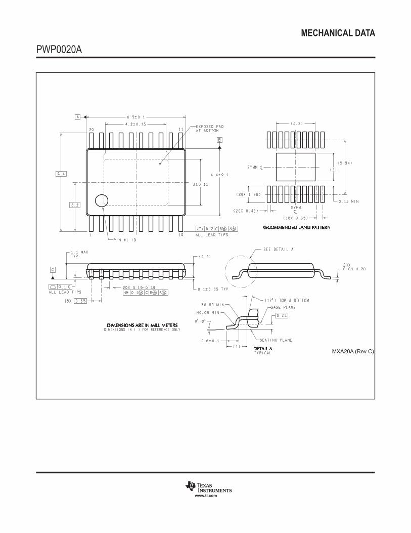
PWP0020A
www.ti.com
MXA20A (Rev C)

IMPORTANT NOTICE
Texas Instruments Incorporated (TI) reserves the right to make corrections, enhancements, improvements and other changes to itssemiconductor products and services per JESD46, latest issue, and to discontinue any product or service per JESD48, latest issue. Buyersshould obtain the latest relevant information before placing orders and should verify that such information is current and complete.TI’s published terms of sale for semiconductor products (http://www.ti.com/sc/docs/stdterms.htm) apply to the sale of packaged integratedcircuit products that TI has qualified and released to market. Additional terms may apply to the use or sale of other types of TI products andservices.Reproduction of significant portions of TI information in TI data sheets is permissible only if reproduction is without alteration and isaccompanied by all associated warranties, conditions, limitations, and notices. TI is not responsible or liable for such reproduceddocumentation. Information of third parties may be subject to additional restrictions. Resale of TI products or services with statementsdifferent from or beyond the parameters stated by TI for that product or service voids all express and any implied warranties for theassociated TI product or service and is an unfair and deceptive business practice. TI is not responsible or liable for any such statements.Buyers and others who are developing systems that incorporate TI products (collectively, “Designers”) understand and agree that Designersremain responsible for using their independent analysis, evaluation and judgment in designing their applications and that Designers havefull and exclusive responsibility to assure the safety of Designers' applications and compliance of their applications (and of all TI productsused in or for Designers’ applications) with all applicable regulations, laws and other applicable requirements. Designer represents that, withrespect to their applications, Designer has all the necessary expertise to create and implement safeguards that (1) anticipate dangerousconsequences of failures, (2) monitor failures and their consequences, and (3) lessen the likelihood of failures that might cause harm andtake appropriate actions. Designer agrees that prior to using or distributing any applications that include TI products, Designer willthoroughly test such applications and the functionality of such TI products as used in such applications.TI’s provision of technical, application or other design advice, quality characterization, reliability data or other services or information,including, but not limited to, reference designs and materials relating to evaluation modules, (collectively, “TI Resources”) are intended toassist designers who are developing applications that incorporate TI products; by downloading, accessing or using TI Resources in anyway, Designer (individually or, if Designer is acting on behalf of a company, Designer’s company) agrees to use any particular TI Resourcesolely for this purpose and subject to the terms of this Notice.TI’s provision of TI Resources does not expand or otherwise alter TI’s applicable published warranties or warranty disclaimers for TIproducts, and no additional obligations or liabilities arise from TI providing such TI Resources. TI reserves the right to make corrections,enhancements, improvements and other changes to its TI Resources. TI has not conducted any testing other than that specificallydescribed in the published documentation for a particular TI Resource.Designer is authorized to use, copy and modify any individual TI Resource only in connection with the development of applications thatinclude the TI product(s) identified in such TI Resource. NO OTHER LICENSE, EXPRESS OR IMPLIED, BY ESTOPPEL OR OTHERWISETO ANY OTHER TI INTELLECTUAL PROPERTY RIGHT, AND NO LICENSE TO ANY TECHNOLOGY OR INTELLECTUAL PROPERTYRIGHT OF TI OR ANY THIRD PARTY IS GRANTED HEREIN, including but not limited to any patent right, copyright, mask work right, orother intellectual property right relating to any combination, machine, or process in which TI products or services are used. Informationregarding or referencing third-party products or services does not constitute a license to use such products or services, or a warranty orendorsement thereof. Use of TI Resources may require a license from a third party under the patents or other intellectual property of thethird party, or a license from TI under the patents or other intellectual property of TI.TI RESOURCES ARE PROVIDED “AS IS” AND WITH ALL FAULTS. TI DISCLAIMS ALL OTHER WARRANTIES ORREPRESENTATIONS, EXPRESS OR IMPLIED, REGARDING RESOURCES OR USE THEREOF, INCLUDING BUT NOT LIMITED TOACCURACY OR COMPLETENESS, TITLE, ANY EPIDEMIC FAILURE WARRANTY AND ANY IMPLIED WARRANTIES OFMERCHANTABILITY, FITNESS FOR A PARTICULAR PURPOSE, AND NON-INFRINGEMENT OF ANY THIRD PARTY INTELLECTUALPROPERTY RIGHTS. TI SHALL NOT BE LIABLE FOR AND SHALL NOT DEFEND OR INDEMNIFY DESIGNER AGAINST ANY CLAIM,INCLUDING BUT NOT LIMITED TO ANY INFRINGEMENT CLAIM THAT RELATES TO OR IS BASED ON ANY COMBINATION OFPRODUCTS EVEN IF DESCRIBED IN TI RESOURCES OR OTHERWISE. IN NO EVENT SHALL TI BE LIABLE FOR ANY ACTUAL,DIRECT, SPECIAL, COLLATERAL, INDIRECT, PUNITIVE, INCIDENTAL, CONSEQUENTIAL OR EXEMPLARY DAMAGES INCONNECTION WITH OR ARISING OUT OF TI RESOURCES OR USE THEREOF, AND REGARDLESS OF WHETHER TI HAS BEENADVISED OF THE POSSIBILITY OF SUCH DAMAGES.Unless TI has explicitly designated an individual product as meeting the requirements of a particular industry standard (e.g., ISO/TS 16949and ISO 26262), TI is not responsible for any failure to meet such industry standard requirements.Where TI specifically promotes products as facilitating functional safety or as compliant with industry functional safety standards, suchproducts are intended to help enable customers to design and create their own applications that meet applicable functional safety standardsand requirements. Using products in an application does not by itself establish any safety features in the application. Designers mustensure compliance with safety-related requirements and standards applicable to their applications. Designer may not use any TI products inlife-critical medical equipment unless authorized officers of the parties have executed a special contract specifically governing such use.Life-critical medical equipment is medical equipment where failure of such equipment would cause serious bodily injury or death (e.g., lifesupport, pacemakers, defibrillators, heart pumps, neurostimulators, and implantables). Such equipment includes, without limitation, allmedical devices identified by the U.S. Food and Drug Administration as Class III devices and equivalent classifications outside the U.S.TI may expressly designate certain products as completing a particular qualification (e.g., Q100, Military Grade, or Enhanced Product).Designers agree that it has the necessary expertise to select the product with the appropriate qualification designation for their applicationsand that proper product selection is at Designers’ own risk. Designers are solely responsible for compliance with all legal and regulatoryrequirements in connection with such selection.Designer will fully indemnify TI and its representatives against any damages, costs, losses, and/or liabilities arising out of Designer’s non-compliance with the terms and provisions of this Notice.
Mailing Address: Texas Instruments, Post Office Box 655303, Dallas, Texas 75265Copyright © 2018, Texas Instruments Incorporated

Mouser Electronics
Authorized Distributor
Click to View Pricing, Inventory, Delivery & Lifecycle Information: Texas Instruments:
LM26420XMH/NOPB LM26420XMHX/NOPB LM26420XSQ/NOPB LM26420XSQX/NOPB LM26420YMH/NOPB
LM26420YMHX/NOPB LM26420YSQ/NOPB LM26420YSQX/NOPB