lm25011(q,a,aq) - texas instruments · 4 lm25011, lm25011-q1, lm25011a, lm25011a-q1...
TRANSCRIPT

FB
SW
L1
RFB2
LM25011
BSTCBST
D1
CS
RT
VIN
6V to 42VInput
CIN
SS
CSS
RT
SGND
PGDCSG
RS
RPGD
VPGD
COUT
RFB1
VOUT
PowerGood
Product
Folder
Order
Now
Technical
Documents
Tools &
Software
Support &Community
An IMPORTANT NOTICE at the end of this data sheet addresses availability, warranty, changes, use in safety-critical applications,intellectual property matters and other important disclaimers. PRODUCTION DATA.
LM25011, LM25011-Q1, LM25011A, LM25011A-Q1SNVS617H –APRIL 2009–REVISED NOVEMBER 2014
LM25011, LM25011-Q1, LM25011A, LM25011A-Q1 42-V 2-A Constant On-Time SwitchingRegulator With Adjustable Current Limit
1
1 Features1• LM25011-Q1 is an Automotive Grade Product that
is AEC-Q100 Grade 1 Qualified (–40°C to +125°COperating Junction Temperature)
• LM25011A Allows Low-Dropout Operation at HighSwitching Frequency
• Input Operating Voltage Range: 6 V to 42 V• Absolute Maximum Input Rating: 45 V• Integrated 2-A N-Channel Buck Switch• Adjustable Current Limit Allows for Smaller
Inductor• Adjustable Output Voltage from 2.51 V• Minimum Ripple Voltage at VOUT
• Power Good Output• Switching Frequency Adjustable to 2 MHz• COT Topology Features:
– Switching Frequency Remains NearlyConstant with Load Current and Input VoltageVariations
– Ultra-Fast Transient Response– No Loop Compensation Required– Stable Operation with Ceramic Output
Capacitors– Allows for Smaller Output Capacitor and
Current Sense Resistor• Adjustable Soft-Start Timing• Thermal Shutdown• Precision 2% Feedback Reference• Package: 10-Pin, HVSSOP• Create a Custom Design Using the LM25011
Family with the WEBENCH Power Designer
2 Applications• Automotive Safety• Infotainment• Telecommunication• Front Camera
3 DescriptionThe LM25011 constant on-time step-down switchingregulator features all the functions needed toimplement a low-cost, efficient, buck bias regulatorcapable of supplying up to 2 A of load current. Thishigh-voltage regulator contains an N-Channel Buckswitch, a startup regulator, current limit detection, andinternal ripple control. The constant on-timeregulation principle requires no loop compensation,results in fast load transient response, and simplifiescircuit implementation. The operating frequencyremains constant with line and load. The adjustablevalley current limit detection results in a smoothtransition from constant voltage to constant currentmode when current limit is reached, without the useof current limit foldback. The PGD output indicatesthe output voltage has increased to within 5% of theexpected regulation value. Additional featuresinclude: Low output ripple, VIN under-voltage lock-out, adjustable soft-start timing, thermal shutdown,gate drive pre-charge, gate drive under-voltage lock-out, and maximum duty cycle limit.
The LM25011A has a shorter minimum off-time thanthe LM25011, which allows for higher frequencyoperation at low input voltages.
Device Information(1)
PART NUMBER PACKAGE BODY SIZE (NOM)LM25011 / -Q1
HVSSOP (10) 3.00 mm × 3.00 mmLM25011A / -Q1
(1) For all available packages, see the orderable addendum atthe end of the data sheet.
Typical Application

2
LM25011, LM25011-Q1, LM25011A, LM25011A-Q1SNVS617H –APRIL 2009–REVISED NOVEMBER 2014 www.ti.com
Product Folder Links: LM25011 LM25011-Q1 LM25011A LM25011A-Q1
Submit Documentation Feedback Copyright © 2009–2014, Texas Instruments Incorporated
Table of Contents1 Features .................................................................. 12 Applications ........................................................... 13 Description ............................................................. 14 Revision History..................................................... 25 Pin Configuration and Functions ......................... 36 Specifications......................................................... 4
6.1 Absolute Maximum Ratings ..................................... 46.2 Handling Ratings: LM25011...................................... 46.3 Handling Ratings: LM25011-Q1................................ 46.4 Recommended Operating Conditions....................... 46.5 Thermal Information .................................................. 56.6 Electrical Characteristics........................................... 66.7 Typical Characteristics .............................................. 7
7 Detailed Description ............................................ 107.1 Overview ................................................................. 107.2 Functional Block Diagram ....................................... 107.3 Feature Description................................................. 10
7.4 Device Functional Modes........................................ 158 Application and Implementation ........................ 16
8.1 Application Information............................................ 168.2 Typical Application .................................................. 16
9 Power Supply Recommendations ...................... 2310 Layout................................................................... 23
10.1 Layout Guidelines ................................................. 2310.2 Layout Example .................................................... 2310.3 Power Dissipation ................................................. 23
11 Device and Documentation Support ................. 2411.1 Custom Design with WEBENCH Tools................. 2411.2 Receiving Notification of Documentation Updates 2411.3 Related Links ........................................................ 2411.4 Trademarks ........................................................... 2411.5 Electrostatic Discharge Caution............................ 2411.6 Glossary ................................................................ 24
12 Mechanical, Packaging, and OrderableInformation ........................................................... 24
4 Revision HistoryNOTE: Page numbers for previous revisions may differ from page numbers in the current version.
Changes from Revision G (February 2013) to Revision H Page
• Added Pin Configuration and Functions section, Handling Rating table, Feature Description section, DeviceFunctional Modes, Application and Implementation section, Power Supply Recommendations section, Layoutsection, Device and Documentation Support section, and Mechanical, Packaging, and Orderable Informationsection ................................................................................................................................................................................... 1
Changes from Revision F (February 2013) to Revision G Page
• Changed layout of National Semiconductor Data Sheet to TI format .................................................................................. 23

SW
BST
FB
CS
CSG
RT
VIN
PGD
SGND
SS
Exposed Pad on BottomConnect to Ground
1
2
3
4
5
10
9
8
7
6
3
LM25011, LM25011-Q1, LM25011A, LM25011A-Q1www.ti.com SNVS617H –APRIL 2009–REVISED NOVEMBER 2014
Product Folder Links: LM25011 LM25011-Q1 LM25011A LM25011A-Q1
Submit Documentation FeedbackCopyright © 2009–2014, Texas Instruments Incorporated
5 Pin Configuration and Functions
10-PinHVSSOP Package
Top View
Pin FunctionsPIN I/O DESCRIPTION APPLICATION INFORMATION
NUMBER NAME1 VIN I Input supply voltage Operating input range is 6 V to 42 V. Transient capability is 45 V.
A low ESR capacitor must be placed as close as possible to theVIN and SGND pins.
2 RT I On-time Control An external resistor from VIN to this pin sets the buck switch on-time and the switching frequency.
3 PGD – Power Good Logic output indicates when the voltage at the FB pin hasincreased to above 95% of the internal reference voltage.Hysteresis is provided. An external pull-up resistor to a voltageless than 7 V is required.
4 SS I Soft-Start An internal current source charges an external capacitor toprovide the soft-start function.
5 SGND Signal Ground Ground for all internal circuitry other than the current limit sensecircuit.
6 FB I Feedback Internally connected to the regulation comparator. The regulationlevel is 2.51 V.
7 CSG – Current Sense Ground Ground connection for the current limit sensing circuit. Connect toground and to the current sense resistor.
8 CS I Current sense Connect to the current sense resistor and the anode of the free-wheeling diode.
9 SW O Switching Node Internally connected to the buck switch source. Connect to theexternal inductor, cathode of the free-wheeling diode, andbootstrap capacitor.
10 BST I Bootstrap capacitor connection ofthe buck switch gate driver.
Connect a 0.1-µF capacitor from SW to this pin. The capacitor ischarged during the buck switch off-time via an internal diode.
- EP – Exposed Pad Exposed pad on the underside of the package. This pad shouldbe soldered to the PC board ground plane to aid in heatdissipation.

4
LM25011, LM25011-Q1, LM25011A, LM25011A-Q1SNVS617H –APRIL 2009–REVISED NOVEMBER 2014 www.ti.com
Product Folder Links: LM25011 LM25011-Q1 LM25011A LM25011A-Q1
Submit Documentation Feedback Copyright © 2009–2014, Texas Instruments Incorporated
(1) Absolute Maximum Ratings(1) are limits beyond which damage to the device may occur. Recommended Operating Conditions areconditions under which operation of the device is intended to be functional. For specifications and test conditions, see the ElectricalCharacteristics .
6 Specifications
6.1 Absolute Maximum Ratings (1)
MIN MAX UNITVIN to SGND (TJ = 25°C) 45 VBST to SGND 52 VSW to SGND (Steady State) –1.5 45 VBST to SW –0.3 7 VCS to CSG –0.3 0.3 VCSG to SGND –0.3 0.3 VPGD to SGND –0.3 7 VSS to SGND –0.3 3 VRT to SGND –0.3 1 VFB to SGND –0.3 7 VFor soldering specs, see www.ti.com/packaging.Junction Temperature 150 °C
(1) JEDEC document JEP155 states that 500-V HBM allows safe manufacturing with a standard ESD control process.(2) JEDEC document JEP157 states that 250-V CDM allows safe manufacturing with a standard ESD control process.
6.2 Handling Ratings: LM25011MIN MAX UNIT
Tstg Storage temperature range –65 150 °C
V(ESD) Electrostatic discharge
Human body model (HBM), per ANSI/ESDA/JEDEC JS-001,all pins (1)
2000
VCharged device model (CDM), per JEDEC specificationJESD22-C101, all pins (2)
750
(1) AEC Q100-002 indicates HBM stressing is done in accordance with the ANSI/ESDA/JEDEC JS-001 specification.
6.3 Handling Ratings: LM25011-Q1MIN MAX UNIT
Tstg Storage temperature range –65 150 °C
V(ESD) Electrostatic discharge
Human body model (HBM), per AEC Q100-002 (1) 2000
VCharged device model (CDM), perAEC Q100-011
Corner pins (1, 5, 6,and 10)
750
Other pins 750
(1) Absolute Maximum Ratings(1) are limits beyond which damage to the device may occur. Recommended Operating Conditions areconditions under which operation of the device is intended to be functional. For specifications and test conditions, see the ElectricalCharacteristics .
6.4 Recommended Operating Conditionsover operating free-air temperature range (unless otherwise noted) (1)
MIN MAX UNITVIN Voltage 6.0 42 VJunction Temperature –40 125 °C

5
LM25011, LM25011-Q1, LM25011A, LM25011A-Q1www.ti.com SNVS617H –APRIL 2009–REVISED NOVEMBER 2014
Product Folder Links: LM25011 LM25011-Q1 LM25011A LM25011A-Q1
Submit Documentation FeedbackCopyright © 2009–2014, Texas Instruments Incorporated
(1) For more information about traditional and new thermal metrics, see the IC Package Thermal Metrics application report, SPRA953.
6.5 Thermal Information
THERMAL METRIC (1) HVSSOP (DGQ)UNIT
10 PINSRθJA Junction-to-ambient thermal resistance 48
°C/W
RθJC(top) Junction-to-case (top) thermal resistance 54.3RθJB Junction-to-board thermal resistance 34.2ψJT Junction-to-top characterization parameter 4.0ψJB Junction-to-board characterization parameter 33.9RθJC(bot) Junction-to-case (bottom) thermal resistance 10

6
LM25011, LM25011-Q1, LM25011A, LM25011A-Q1SNVS617H –APRIL 2009–REVISED NOVEMBER 2014 www.ti.com
Product Folder Links: LM25011 LM25011-Q1 LM25011A LM25011A-Q1
Submit Documentation Feedback Copyright © 2009–2014, Texas Instruments Incorporated
(1) Current flow out of a pin is indicated as a negative number.(2) All hot and cold limits are specified by correlating the electrical characteristics to process and temperature variations and applying
statistical process control.(3) The junction temperature (TJ in °C) is calculated from the ambient temperature (TA in °C) and power dissipation (PD in watts) as follows:
TJ = TA + (PD × RθJA ) where RθJA (in °C/W) is the package thermal impedance provided in the Thermal Information section.
6.6 Electrical CharacteristicsTypical values correspond to TJ = 25°C. Minimum and maximum limits apply over –40°C to 125°C junction temperature rangeunless otherwise stated. Unless otherwise stated, the following conditions apply: VIN = 12 V, RT = 50 kΩ. (1) (2) (3)
PARAMETER TEST CONDITIONS MIN TYP MAX UNITINPUT (VIN PIN)
IIN Input operating current Non-switching, FB = 3 V 1200 1600 µAUVLOVIN VIN undervoltage lock-out threshold VIN increasing 4.6 5.3 5.9 V
VIN undervoltage lock-out threshold hysteresis 200 mVSWITCH CHARACTERISTICS
RDS(ON) Buck Switch RDS(ON) ITEST = 200 mA 0.3 0.6 ΩUVLOGD Gate Drive UVLO BST-SW 2.4 3.4 4.4 V
UVLOGD Hysteresis 350 mVPre-charge switch voltage ITEST = 10 mA into SW pin 1.4 VPre-charge switch on-time 120 ns
SOFT-START PINVSS Pullup voltage 2.51 VISS Internal current source 10 µA
VSS-SH Shutdown threshold 70 140 mVCURRENT LIMIT
VILIM Threshold voltage at CS –146 –130 –115 mVCS bias current FB = 3 V –120 µACSG bias current FB = 3 V –35 µA
ON TIMER, RT PINtON - 1 On-time VIN = 12 V, RT = 50 kΩ 150 200 250 nstON - 2 On-time VIN = 32 V, RT = 50 kΩ 75 nstON - 3 On-time (current limit) LM25011 VIN = 12 V, RT = 50 kΩ 100 nstON - 3 On-time (current limit) LM25011A VIN = 12 V, RT = 50 kΩ 200 nstON - 4 On-time VIN = 12 V, RT = 301 kΩ 1020 nstON - 5 On-time VIN = 9 V, RT = 30.9 kΩ 130 171 215 nstON - 6 On-time VIN = 12 V, RT = 30.9 kΩ 105 137 170 nstON - 7 On-time VIN = 16 V, RT = 30.9 kΩ 79 109 142 ns
OFF TIMERtOFF Minimum off-time (LM25011) 90 150 208 ns
Minimum off-time (LM25011A) 52 75 93REGULATION COMPARATOR (FB PIN)
VREF FB regulation threshold SS pin = steady state 2.46 2.51 2.56 VFB bias current FB = 3 V 100 nA
POWER GOOD (PGD PIN)Threshold at FB, with respect to VREF FB increasing 91% 95%Threshold hysteresis 3.3%
PGDVOL Low state voltage IPGD = 1 mA, FB = 0 V 125 180 mVPGDLKG Off state leakage VPGD = 7 V, FB = 3 V 0.1 µA
THERMAL SHUTDOWNTSD Thermal shutdown Junction temperature increasing 155 °C
Thermal shutdown hysteresis 20 °C
7
LM25011, LM25011-Q1, LM25011A, LM25011A-Q1www.ti.com SNVS617H –APRIL 2009–REVISED NOVEMBER 2014
Product Folder Links: LM25011 LM25011-Q1 LM25011A LM25011A-Q1
Submit Documentation FeedbackCopyright © 2009–2014, Texas Instruments Incorporated
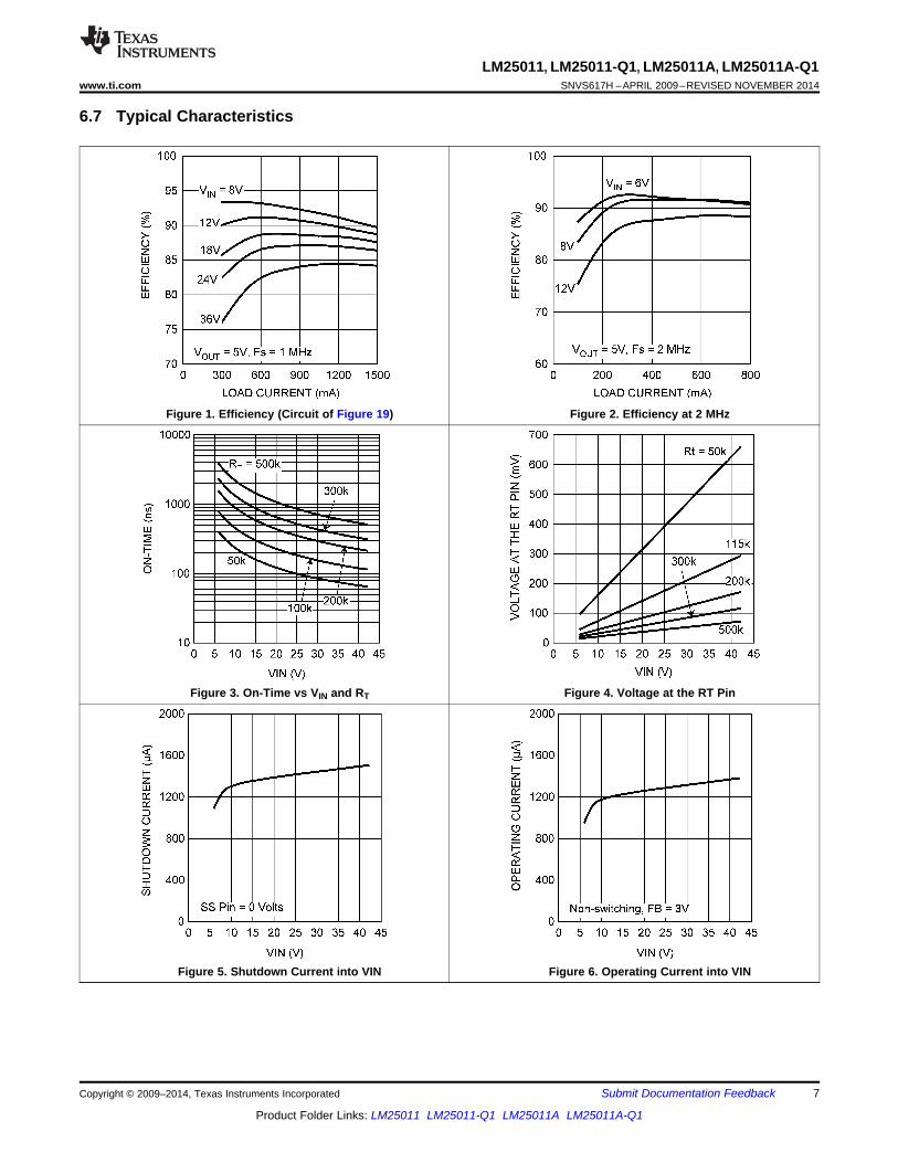
6.7 Typical Characteristics
Figure 1. Efficiency (Circuit of Figure 19) Figure 2. Efficiency at 2 MHz
Figure 3. On-Time vs VIN and RT Figure 4. Voltage at the RT Pin
Figure 5. Shutdown Current into VIN Figure 6. Operating Current into VIN

8
LM25011, LM25011-Q1, LM25011A, LM25011A-Q1SNVS617H –APRIL 2009–REVISED NOVEMBER 2014 www.ti.com
Product Folder Links: LM25011 LM25011-Q1 LM25011A LM25011A-Q1
Submit Documentation Feedback Copyright © 2009–2014, Texas Instruments Incorporated
Typical Characteristics (continued)
Figure 7. PGD Low Voltage vs Sink Current Figure 8. Reference Voltage vs Temperature
Figure 9. Current Limit Threshold vs Temperature Figure 10. Operating Current vs Temperature
Figure 11. VIN UVLO vs Temperature Figure 12. SS Pin Shutdown Threshold vs Temperature

-40 -20 0 20 40 60 80 100 12050
70
90
110
130
150
170
190
MIN
IMU
M O
FF
-TIM
E (
ns)
JUNCTION TEMPERATURE (°C)
LM25011A
LM25011
9
LM25011, LM25011-Q1, LM25011A, LM25011A-Q1www.ti.com SNVS617H –APRIL 2009–REVISED NOVEMBER 2014
Product Folder Links: LM25011 LM25011-Q1 LM25011A LM25011A-Q1
Submit Documentation FeedbackCopyright © 2009–2014, Texas Instruments Incorporated
Typical Characteristics (continued)
Figure 13. On-Time vs Temperature Figure 14. Minimum Off-Time vs Temperature

SS
RT
FB
VIN
SW
VIN
BST
L1
CBST
D1
SD
CS
LEVELSHIFT
ON TIMER
FINISH START
LOGIC
Gate Drive
UVLO
5V REGULATOR
Input
CL
CL
2.5V
REGULATIONCOMPARATOR
LM25011(A)
10PA
CURRENTLIMIT COMPARATOR
FINISHSTART
OFF TIMERTHERMAL
SHUTDOWN
FCIC
CONTROL
PGD
2.375V
0.8V
RPGD
CSG
PowerGood
125 mV
UVLO
SGND
RS
+-CURRENT LIMIT
THRESHOLD
+
-
6V to 42V
CBYPCIN
RT
CSS
COUT
VOUT
RFB2
RFB2
+
-
+
-
Pre - Chg
10
LM25011, LM25011-Q1, LM25011A, LM25011A-Q1SNVS617H –APRIL 2009–REVISED NOVEMBER 2014 www.ti.com
Product Folder Links: LM25011 LM25011-Q1 LM25011A LM25011A-Q1
Submit Documentation Feedback Copyright © 2009–2014, Texas Instruments Incorporated
7 Detailed Description
7.1 OverviewThe LM25011 constant on-time step-down switching regulator features all the functions needed to implement alow-cost, efficient buck bias power converter capable of supplying up to 2.0 A to the load. This high-voltageregulator contains an N-Channel buck switch, is easy to implement, and is available in a 10-pin VSSOP,PowerPAD power enhanced package. The operation of the regulator is based on a constant on-time controlprinciple with the on-time inversely proportional to the input voltage. This feature results in the operatingfrequency remaining relatively constant with load and input voltage variations. The constant on-time feedbackcontrol principle requires no loop compensation resulting in very fast load transient response. The adjustablevalley current limit detection results in a smooth transition from constant voltage to constant current when currentlimit is reached. To aid in controlling excessive switch current due to a possible saturating inductor, the on-time isreduced by approximately 40% when the current limit is detected. The Power Good output (PGD pin) indicateswhen the output voltage is within 5% of the expected regulation voltage.
The LM25011 can be implemented to efficiently step-down higher voltages in non-isolated applications.Additional features include: low output ripple, VIN under-voltage lock-out, adjustable soft-start timing, thermalshutdown, gate drive pre-charge, gate drive under-voltage lock-out, and maximum duty-cycle limit.
7.2 Functional Block Diagram
7.3 Feature Description
7.3.1 Control Circuit OverviewThe LM25011 buck regulator employs a control principle based on a comparator and a one-shot on-timer, withthe output voltage feedback (FB) compared to an internal reference (2.51 V). If the FB voltage is below thereference, the internal buck switch is switched on for the one-shot timer period which is a function of the inputvoltage and the programming resistor (RT). Following the on-time, the switch remains off until the FB voltage fallsbelow the reference, but never less than the minimum off-time forced by the off-time one-shot timer. When theFB pin voltage falls below the reference and the off-time one-shot period expires, the buck switch is then turnedon for another on-time one-shot period.

RT =VOUT - (VIN x FS x 15 ns)
FS x 4.1 x 10⁻¹¹- 500:
tON =(VIN)
4.1 x 10⁻¹¹ x (RT + 500:)
+ 15 ns
FS =VOUT
2 x L1 x 1.19 x 1021
RL x RT2
DC =tON
tON + tOFF == tON x FS
VOUT
VIN
FS =VOUT
(4.1 x 10⁻¹¹ x (RT + 0.5k)) + (VIN x 15 ns)
11
LM25011, LM25011-Q1, LM25011A, LM25011A-Q1www.ti.com SNVS617H –APRIL 2009–REVISED NOVEMBER 2014
Product Folder Links: LM25011 LM25011-Q1 LM25011A LM25011A-Q1
Submit Documentation FeedbackCopyright © 2009–2014, Texas Instruments Incorporated
Feature Description (continued)When in regulation, the LM25011 operates in continuous conduction mode at heavy load currents anddiscontinuous conduction mode at light load currents. In continuous conduction mode, the inductor current isalways greater than zero and the operating frequency remains relatively constant with load and line variations.The minimum load current for continuous conduction mode is one-half of the ripple current amplitude of theinductor. The approximate operating frequency is calculated as follows:
(1)
The buck switch duty cycle is approximately equal to:
(2)
When the load current is less than one-half of the ripple current amplitude of the inductor, the circuit operates indiscontinuous conduction mode. The off-time is longer than in continuous conduction mode while the inductorcurrent is zero, causing the switching frequency to reduce as the load current is reduced. Conversion efficiency ismaintained at light loads because the switching losses are reduced with the reduction in load and frequency. Theapproximate discontinuous operating frequency can be calculated as follows:
(3)
where RL = the load resistance, and L1 is the inductor in the circuit.
The output voltage is set by the two feedback resistors (RFB1, RFB2 in the Functional Block Diagram ). Theregulated output voltage is calculated as follows:
VOUT = 2.51 V × (RFB1 + RFB2) / RFB1 (4)
Ripple voltage, which is required at the input of the regulation comparator for proper output regulation, isgenerated internally in the LM25011, and externally when the LM25011A is used. In the LM25011 the ERM(emulated ripple mode) control circuit generates the required internal ripple voltage from the ripple waveform atthe CS pin. The LM25011A, which is designed for higher frequency operation, requires additional ripple voltagewhich must be generated externally and provided to the FB pin. This is described in the Application andImplementation section.
7.3.2 On-Time TimerThe on-time for the LM25011/LM25011A is determined by the RT resistor and the input voltage (VIN), calculatedfrom:
(5)
The inverse relationship with VIN results in a nearly constant frequency as VIN is varied. To set a specificcontinuous conduction mode switching frequency (FS), the RT resistor is determined from the following:
(6)
The on-time must be chosen greater than 90 ns for proper operation. Equation 1, Equation 5, and Equation 6 arevalid only during normal operation; that is, the circuit is not in current limit. When the LM25011 operates incurrent limit, the on-time is reduced by approximately 40% (this feature is not present in LM25011A). This featurereduces the peak inductor current which may be excessively high if the load current and the input voltage aresimultaneously high. This feature operates on a cycle-by-cycle basis until the load current is reduced and the

CurrentLimit Threshold
NormalOperation
Load CurrentIncreases
Current Limited
'I
Inductor Current
DecreasesLoad Current
NormalOperation
Voltage at the FB Pin
2.51V
Voltage at the CS Pin
0V
IPK
IO1
IO2
IOCL
12
LM25011, LM25011-Q1, LM25011A, LM25011A-Q1SNVS617H –APRIL 2009–REVISED NOVEMBER 2014 www.ti.com
Product Folder Links: LM25011 LM25011-Q1 LM25011A LM25011A-Q1
Submit Documentation Feedback Copyright © 2009–2014, Texas Instruments Incorporated
Feature Description (continued)output voltage resumes its normal regulated value. The maximum continuous current into the RT pin must beless than 2 mA. For high-frequency applications, the maximum switching frequency is limited at the maximuminput voltage by the minimum on-time one-shot period (90 ns). At minimum input voltage the maximum switchingfrequency is limited by the minimum off-time one-shot period which, if reached, prevents achievement of theproper duty cycle.
7.3.3 Current LimitCurrent limit detection occurs during the off-time by monitoring the voltage across the external current senseresistor RS. Referring to the Functional Block Diagram , during the off-time the recirculating current flows throughthe inductor, through the load, through the sense resistor, and through D1 to the inductor. If the voltage acrossthe sense resistor exceeds the threshold (VILIM), the current limit comparator output switches to delay the start ofthe next on-time period. The next on-time starts when the recirculating current decreases such that the voltageacross RS reduces to the threshold and the voltage at FB is below 2.51 V. The operating frequency is typicallylower due to longer-than-normal off-times. When current limit is detected, the on-time is reduced byapproximately 40% (only in LM25011) if the voltage at the FB pin is below its threshold when the voltage acrossRS reduces to its threshold (VOUT is low due to current limiting).
Figure 15 illustrates the inductor current waveform during normal operation and in current limit. During the firstnormal operation, the load current is I01, the average of the inductor current waveform. As the load resistance isreduced, the inductor current increases until the lower peak of the inductor ripple current exceeds the threshold.During the current limited portion of Figure 15, each on-time is reduced by approximately 40%, resulting in lowerripple amplitude for the inductor current. During this time the LM25011 is in a constant-current mode with anaverage load current equal to the current limit threshold plus half the ripple amplitude (IOCL), and the outputvoltage is below the normal regulated value. Normal operation resumes when the load current is reduced (to IO2),allowing VOUT and the on-time to return to their normal values. Note that in the second period of normaloperation, even though the peak current of the inductor exceeds the current limit threshold during part of eachcycle, the circuit is not in current limit because the inductor current falls below the current limit threshold duringeach off-time. The peak current allowed through the buck switch is 3.5 A and the maximum allowed averagecurrent is 2.0 A.
Figure 15. Normal and Current Limit Operation

Voltage at CS
0V
VRIPPLE
tOFF tON
Inductor Current 'I
13
LM25011, LM25011-Q1, LM25011A, LM25011A-Q1www.ti.com SNVS617H –APRIL 2009–REVISED NOVEMBER 2014
Product Folder Links: LM25011 LM25011-Q1 LM25011A LM25011A-Q1
Submit Documentation FeedbackCopyright © 2009–2014, Texas Instruments Incorporated
Feature Description (continued)7.3.4 Ripple RequirementsThe LM25011 requires about 25 mVP-P of ripple voltage at the CS pin. Higher switching frequencies may requiremore ripple. That ripple voltage is generated by the decreasing recirculating current (the inductor ripple current)through RS during the off-time. See Figure 16.
Figure 16. CS Pin Waveform
The ripple voltage is equal to:VRIPPLE = ΔI × RS (7)
where ΔI is the inductor current ripple amplitude, and RS is the current-sense resistor at the CS pin.
More ripple can be achieved by decreasing the inductor value.
The LM25011A, with its shorter minimum off-time, typically will require more ripple than the LM25011. Anexternal circuit to increase the effective ripple voltage may be needed. Different methods of generating this rippleare explained in the External Components section.
7.3.5 N-Channel Buck Switch and DriverThe LM25011 integrates an N-Channel buck switch and associated floating high-voltage gate driver. The gatedriver circuit works in conjunction with an external bootstrap capacitor (CBST) and an internal high-voltage diode.A 0.1-µF capacitor connected between BST and SW provides the supply voltage for the driver during the on-time. During each off-time, the SW pin is at approximately –1 V, and CBST is recharged from the internal 5-Vregulator for the next on-time. The minimum off-time ensures a sufficient time each cycle to recharge thebootstrap capacitor.
In applications with relatively high output voltage and low minimum load current, the internal pre-charge device ofthe LM25011 may not pull the SW pin sufficiently low during the off-time to maintain the voltage on the bootstrapcapacitor. If the bootstrap capacitor (CBST) discharges during the long off-times, and the regulator will cycle onand off at a low frequency. Decreasing the values of the feedback resistors RFB1 and RFB2 to provide a minimumload of typically 1mA at nominal VOUT will increase the minimum switching frequency and maintain sufficientbootstrap capacitor voltage.
7.3.6 Soft-StartThe soft-start feature allows the converter to gradually reach a steady-state operating point, thereby reducingstartup stresses and current surges. Upon turn-on, when VIN reaches its undervoltage lock-out threshold aninternal 10-µA current source charges the external capacitor at the SS pin to 2.51 V (t1 in Figure 17). Theramping voltage at SS ramps the non-inverting input of the regulation comparator and the output voltage, in acontrolled manner. For proper operation, the soft-start capacitor should be no smaller than 1000 pF.

UVLO
VIN
SW Pin
InductorCurrent
SS Pin
t1
PGD
VOUT
14
LM25011, LM25011-Q1, LM25011A, LM25011A-Q1SNVS617H –APRIL 2009–REVISED NOVEMBER 2014 www.ti.com
Product Folder Links: LM25011 LM25011-Q1 LM25011A LM25011A-Q1
Submit Documentation Feedback Copyright © 2009–2014, Texas Instruments Incorporated
Feature Description (continued)The LM25011 can be employed as a tracking regulator by applying the controlling voltage to the SS pin. Theoutput voltage of the regulator tracks the applied voltage, gained up by the ratio of the feedback resistors. Theapplied voltage at the SS pin must be within the range of 0.5 V to 2.6 V. The absolute maximum rating for the SSpin is 3.0 V. If the tracking function causes the voltage at the FB pin to go below the thresholds for the PGD pin,the PGD pin will switch low (see the Power Good Output (PGD) section). An internal switch grounds the SS pin ifthe input voltage at VIN is below its undervoltage lock-out threshold or if the thermal shutdown activates. If thetracking function (described above) is used, the tracking voltage applied to the SS pin must be current limited toa maximum of 1 mA.
Figure 17. Startup Sequence
7.3.7 Power Good Output (PGD)The Power Good output (PGD) indicates when the voltage at the FB pin is close to the internal 2.51-V referencevoltage. The rising threshold at the FB pin for the PGD output to switch high is 95% of the internal reference. Thefalling threshold for the PGD output to switch low is approximately 3.3% below the rising threshold.
The PGD pin is internally connected to the drain of an N-channel MOSFET switch. An external pull-up resistor(RPGD), connected to an appropriate voltage not exceeding 7 V, is required at PGD to indicate the LM25011status to other circuitry. When PGD is low, the pin voltage is determined by the current into the pin. See Figure 7,PGD Low Voltage vs Sink Current.

RUN
LM25011SS
CSS
STOP
15
LM25011, LM25011-Q1, LM25011A, LM25011A-Q1www.ti.com SNVS617H –APRIL 2009–REVISED NOVEMBER 2014
Product Folder Links: LM25011 LM25011-Q1 LM25011A LM25011A-Q1
Submit Documentation FeedbackCopyright © 2009–2014, Texas Instruments Incorporated
Feature Description (continued)Upon powering up the LM25011, the PGD pin is high until the voltage at VIN reaches 2 V, at which time PGDswitches low. As VIN is increased, PGD stays low until the output voltage takes the voltage at the FB pin above95% of the internal reference voltage, at which time PGD switches high. As VIN is decreased (during shutdown),PGD remains high until either the voltage at the FB pin falls below approximately 92% of the internal reference orwhen VIN falls below its lower UVLO threshold, whichever occurs first. PGD then switches low, and remains lowuntil VIN falls below 2 V, at which time PGD switches high. If the LM25011 is used as a tracking regulator (seethe Soft-Start section), the PGD output is high as long as the voltage at the FB pin is above the thresholdsmentioned above.
7.3.8 Thermal ShutdownThe LM25011 should be operated so the junction temperature does not exceed 125°C. If the junctiontemperature increases above that, an internal thermal shutdown circuit activates (typically) at 155°C, taking thecontroller to a low-power reset state by disabling the buck switch and taking the SS pin to ground. This featurehelps prevent catastrophic failures from accidental device overheating. When the junction temperature decreasesbelow 135°C (typical hysteresis = 20°C), normal operation resumes.
7.4 Device Functional Modes
7.4.1 Shutdown FunctionThe SS pin can be used to shutdown the LM25011 by grounding the SS pin as shown in Figure 18. Releasingthe pin allows normal operation to resume.
Figure 18. Shutdown Implementation

L1 10 PH
D1
CSS
RS
CIN
CBYPRT
118 k:
10 k:
0.022 PF
80 m:
5V
FB
SW
LM25011
BST
CS
RT
VIN
SS
SGND
PGD
CSG
8V to 36VInput
4.7 PF0.1 PF
RPGD
VPGD
PowerGood
4.99 k:
RFB2
CBST
COUT
RFB1
VOUT
4.99 k:
0.1 PF
10 PF
16
LM25011, LM25011-Q1, LM25011A, LM25011A-Q1SNVS617H –APRIL 2009–REVISED NOVEMBER 2014 www.ti.com
Product Folder Links: LM25011 LM25011-Q1 LM25011A LM25011A-Q1
Submit Documentation Feedback Copyright © 2009–2014, Texas Instruments Incorporated
8 Application and Implementation
NOTEInformation in the following applications sections is not part of the TI componentspecification, and TI does not warrant its accuracy or completeness. TI’s customers areresponsible for determining suitability of components for their purposes. Customers shouldvalidate and test their design implementation to confirm system functionality.
8.1 Application InformationThe LM25011/LM25011-Q1 is a non-synchronous buck regulator designed to operate over a wide input voltagerange and output current. Spreadsheet-based quick-start calculation tools and the on-line WEBENCH® softwarecan be used to create a buck design with the bill of materials, estimated efficiency, and the complete solutioncost.
8.2 Typical Application
8.2.1 LM25011 Example CircuitThe final circuit is shown in Figure 19, and its performance is shown in Figure 20 and Figure 21. The current limitmeasures approximately 1.62 A at VIN = 8 V, and 1.69 A at VIN = 36 V.
Figure 19. Example Circuit
8.2.1.1 Design RequirementsTable 1 shows the design parameters.
Table 1. Design ParametersDESIGN PARAMETER VALUE
Input voltage range 8 V to 36 VOutput voltage 5 VMaximum load current (IOUT(max)) 1.5 AMinimum load current (IOUT(min)) 300 mASwitching frequency (FSW) 1 MHzSoft-start time 5 ms

RT =5 - (8V x 1MHz x 15 ns)
1MHz x 4.1 x 10-11 - 500:= 118.5 k:
tOFF(min) =VIN(min) - VOUT
VIN(min) x FS= 375 ns
8V - 5V8V x 1 MHz
=
tON(min) =VOUT
VIN(max) x FS= 139 ns
5V36V x 1 MHz
=
17
LM25011, LM25011-Q1, LM25011A, LM25011A-Q1www.ti.com SNVS617H –APRIL 2009–REVISED NOVEMBER 2014
Product Folder Links: LM25011 LM25011-Q1 LM25011A LM25011A-Q1
Submit Documentation FeedbackCopyright © 2009–2014, Texas Instruments Incorporated
8.2.1.2 Detailed Design Procedure
8.2.1.2.1 Custom Design with WEBENCH Tools
Click here to create a custom design using the LM25011 device with the WEBENCH® Power Designer.1. Start by entering your VIN, VOUT and IOUT requirements.2. Optimize your design for key parameters like efficiency, footprint and cost using the optimizer dial and
compare this design with other possible solutions from Texas Instruments.3. WEBENCH Power Designer provides you with a customized schematic along with a list of materials with real
time pricing and component availability.4. In most cases, you will also be able to:
– Run electrical simulations to see important waveforms and circuit performance,– Run thermal simulations to understand the thermal performance of your board,– Export your customized schematic and layout into popular CAD formats,– Print PDF reports for the design, and share your design with colleagues.
5. Get more information about WEBENCH tools at www.ti.com/webench.
8.2.1.2.2 External Components
The procedure for calculating the external components is illustrated with a design example using the LM25011.Referring to the Functional Block Diagram , the circuit is to be configured for the following specifications:• VOUT = 5 V• VIN = 8 V to 36 V• Minimum load current for continuous conduction mode IOUT(min) = 300 mA• Maximum load current IOUT(max) = 1.5 A• Switching frequency (FSW) = 1.0 MHz• Soft-start time = 5 ms
RFB2 and RFB1: These resistors set the output voltage, and their ratio is calculated from:RFB2/RFB1 = (VOUT / 2.51 V) – 1 (8)
For this example, RFB2/RFB1 = 0.992. RFB1 and RFB2 should be chosen from standard value resistors in the rangeof 1.0 kΩ to 10 kΩ which satisfy the above ratio. For this example, 4.99 kΩ is chosen for both resistors, providinga 5.02-V output.
RT: This resistor sets the on-time and (by default) the switching frequency. First check that the desired frequencydoes not require an on-time or off-time shorter than the minimum allowed values (90 ns and 150, respectively).The minimum on-time occurs at the maximum input voltage. For this example:
(9)
The minimum off-time occurs at the minimum input voltage. For this example:
(10)
Both the on-time and off-time are acceptable because they are significantly greater than the minimum value foreach. The RT resistor is calculated from Equation 6 using the minimum input voltage:
(11)
A standard value 118-kΩ resistor is selected. The minimum on-time calculates to 152 ns at VIN = 36 V, and themaximum on-time calculates to 672 ns at VIN = 8 V.

Duty Cycle = D = = = 13.9%VOUT
VIN
5V36V
L1(min) =tON(min) x (VIN(max) - VOUT)
IOR(max)= 7.85 PH
18
LM25011, LM25011-Q1, LM25011A, LM25011A-Q1SNVS617H –APRIL 2009–REVISED NOVEMBER 2014 www.ti.com
Product Folder Links: LM25011 LM25011-Q1 LM25011A LM25011A-Q1
Submit Documentation Feedback Copyright © 2009–2014, Texas Instruments Incorporated
L1: The parameters controlled by the inductor are the inductor current ripple amplitude (IOR), and the ripplevoltage amplitude across the current sense resistor RS. The minimum load current is used to determine themaximum allowable ripple to maintain continuous conduction mode (the lower peak does not reach 0 mA). Thisis not a requirement of the LM25011, but serves as a guideline for selecting L1. For this example, the maximumripple current should be less than:
IOR(max) = 2 × IOUT(min) = 600 mAP-P (12)
For applications where the minimum load current is zero, a good starting point for allowable ripple is 20% of themaximum load current. In this case substitute 20% of IOUT(max) for IOUT(min) in Equation 12. The ripple amplitudecalculated in Equation 12 is then used in Equation 13:
(13)
A standard value 10-µH inductor is chosen. Using this inductor value, the maximum ripple current amplitude,which occurs at maximum VIN, calculates to 472 mAP-P, and the peak current is 1736 mA at maximum loadcurrent. Ensure the selected inductor is rated for this peak current. The minimum ripple current, which occurs atminimum VIN, calculates to 200 mAP-P.
RS: The minimum current limit threshold is calculated at maximum load current using the minimum ripple currentcalculated above. The current limit threshold is the lower peak of the inductor current waveform when in currentlimit (see Figure 15).
ILIM = 1.5 A – (0.2 A / 2) = 1.4 A (14)
Current limit detection occurs when the voltage across the sense resistor (RS) reaches the current limit threshold.To allow for tolerances, the sense resistor value is calculated using the minimum threshold specification:
RS = 115 mV / 1.4 A = 82 mΩ (15)
The next smaller standard value, 80 mΩ, is selected. The next step is to ensure that sufficient ripple voltageoccurs across RS with this value sense resistor. As mentioned in the Ripple Requirements section, a minimum of15-mVP-P voltage ripple is required across the RS sense resistor during the off-time to ensure the regulationcircuit operates properly. The ripple voltage is the product of the inductor ripple current amplitude and the senseresistor value. In this case, the minimum ripple voltage calculates to:
VRIPPLE = ΔI × RS = 200 mA × 0.080 Ω = 16 mV (16)
If the ripple voltage had calculated to less than 15 mVP-P, the inductor value would have to be reduced toincrease the ripple current amplitude. This would have required a recalculation of ILIM and RS in the aboveequations. Because the minimum requirement is satisfied in this case, no change is necessary.
The nominal current limit threshold calculates to 1.63 A. The minimum and maximum thresholds calculate to 1.44A and 1.83 A, respectively, using the minimum and maximum limits for the current limit threshold specification.The load current is equal to the threshold current plus one-half of the ripple current. Under normal loadconditions, the maximum power dissipation in RS occurs at maximum load current, and at maximum input voltagewhere the on-time duty cycle is minimum. In this design example, the minimum on-time duty cycle is:
(17)
At maximum load current, the power dissipation in RS is equal to:P(RS) = (1.5 A)2 × 0.080 Ω × (1 – 0.139) = 155 mW (18)
When in current limit the maximum power dissipation in RS calculates toP(RS) = (1.83 A + 0.472 A / 4)2 × 0.080 Ω = 304 mW (19)
Duty cycle is not included in this power calculation because the on-time duty cycle is typically <5% when incurrent limit.
COUT: The output capacitor should typically be no smaller than 3.3 µF, although that is dependent on thefrequency and the desired output characteristics. COUT should be a low ESR good-quality ceramic capacitor.Experimentation is usually necessary to determine the minimum value for COUT, as the nature of the load mayrequire a larger value. A load which creates significant transients requires a larger value for COUT than a non-varying load.

CSS =2.51V
5 ms x 10 PA= 0.02 PF
CIN =IOUT(max) x tON(max)
'V= 2.02 PF
1.5A x 672 ns0.5V
=
19
LM25011, LM25011-Q1, LM25011A, LM25011A-Q1www.ti.com SNVS617H –APRIL 2009–REVISED NOVEMBER 2014
Product Folder Links: LM25011 LM25011-Q1 LM25011A LM25011A-Q1
Submit Documentation FeedbackCopyright © 2009–2014, Texas Instruments Incorporated
CIN and CBYP: The purpose of CIN is to supply most of the switch current during the on-time, and limit the voltageripple at VIN, because it is assumed the voltage source feeding VIN has some amount of source impedance.When the buck switch turns on, the current into VIN suddenly increases to the lower peak of the inductor ripplecurrent, then ramps up to the upper peak, and finally drops to zero at turn-off. The average current during the on-time is the average load current. For a worst case calculation, CIN must supply this average load current duringthe maximum on-time, without letting the voltage at the VIN pin drop below a minimum operating level of 5.5 V.For this exercise 0.5 V is chosen as the maximum allowed input ripple voltage. Using the maximum load current,the minimum value for CIN is calculated from:
(20)
where tON is the maximum on-time, and ΔV is the allowable ripple voltage at VIN. The purpose of CBYP is tominimize transients and ringing due to long lead inductance leading to the VIN pin. A low ESR 0.1-µF ceramicchip capacitor is recommended, and CBYP must be located close to the VIN and SGND pins.
CBST: The recommended value for CBST is 0.1 µF. A high-quality ceramic capacitor with low ESR isrecommended as CBST supplies a surge current to charge the buck switch gate at each turn-on. A low ESR alsohelps ensure a complete recharge during each off-time.
CSS: The capacitor at the SS pin determines the soft-start time, that is, the time for the output voltage to reach itsfinal value (t1 in Figure 17). For a soft-start time of 5 ms, the capacitor value is determined from the following:
(21)
D1: A Schottky diode is recommended. Ultra-fast recovery diodes are not recommended as the high-speedtransitions at the SW pin may affect the regulator operation due to the reverse recovery transients of the diode.The diode must be rated for the maximum input voltage, the maximum load current, and the peak current whichoccurs when the current limit and maximum ripple current are reached simultaneously. The average powerdissipation of the diode is calculated from:
PD1 = VF × IOUT × (1 – D) (22)
where VF is the forward voltage drop of the diode, and D is the on-time duty cycle.
8.2.1.3 Application Curves
Figure 20. Efficiency (Circuit of Figure 19) Figure 21. Frequency vs VIN (Circuit of Figure 19)

Cff >3 x tON(max)
RFB1//RFB2
R1 =VRIPPLE
'I
FB
SW
L1
COUT
RFB2
RFB1
LM25011A
BSTCBST
D1
CS
VOUT
SGND
CSG
RS
R1
R1 =VRIPPLE x (RFB2 + RFB1)
'I x RFB1
20
LM25011, LM25011-Q1, LM25011A, LM25011A-Q1SNVS617H –APRIL 2009–REVISED NOVEMBER 2014 www.ti.com
Product Folder Links: LM25011 LM25011-Q1 LM25011A LM25011A-Q1
Submit Documentation Feedback Copyright © 2009–2014, Texas Instruments Incorporated
8.2.2 Output Ripple ControlHigh frequency applications of the LM25011 or LM25011A are likely to require more ripple voltage than isinternally generated across the RS resistor. Additional ripple can be supplied to the FB pin, in phase with theswitching waveform at the SW pin, for proper operation. The required ripple can be supplied from ripplegenerated at VOUT, through the feedback resistors, as described in Option A: Lowest Cost Configuration . OptionB: Intermediate VOUT Ripple Configuration and Option C: Minimum VOUT Ripple Configuration use one or twoadditional components to provide ripple at the FB pin with lower output ripple at VOUT.
The amount of additional ripple voltage needed at the FB pin is typically in the range of 30 mV to 150 mV. Higherswitching frequencies or higher inductor values (less ripple current) require more external ripple voltage injectedat the FB pin. Insufficient ripple voltage will result in frequency jitter. For a particular application, add only asmuch ripple as needed to stabilize the switching frequency over the required input voltage.
8.2.2.1 Option A: Lowest Cost ConfigurationIn this configuration R1 is installed in series with the output capacitor (COUT) as shown in Figure 22. The ripplecurrent of the inductor passes through R1, generating a ripple voltage at VOUT. The minimum value for R1 is:
(23)
where ΔI is the minimum ripple current amplitude, which occurs at minimum VIN, and VRIPPLE is the peak to peakripple voltage injected at the FB pin.
Figure 22. Option A – Lowest Cost Ripple Configuration
8.2.2.2 Option B: Intermediate VOUT Ripple ConfigurationThis configuration generates less ripple at VOUT than Option A by the addition of capacitor (Cff) as shown inFigure 23.
Because the output ripple is passed by Cff to the FB pin with little or no attenuation, the R1 value and VOUT ripplecan be smaller than in Option A. The minimum value for R1 is calculated from:
(24)
where ΔI is the minimum ripple current amplitude, which occurs at minimum VIN, and VRIPPLE is the peak-to-peakripple voltage injected at the FB pin. The minimum value for Cff is calculated from:
(25)
where tON(max) is the maximum on-time (at minimum VIN), and RFB1//RFB2 is the parallel equivalent of the feedbackresistors.

FB
SW
L1
COUT
RFB2
RFB1
LM25011A
BSTCBST
D1
CS
VOUT
SGND
CSG
RS
R1Cff
21
LM25011, LM25011-Q1, LM25011A, LM25011A-Q1www.ti.com SNVS617H –APRIL 2009–REVISED NOVEMBER 2014
Product Folder Links: LM25011 LM25011-Q1 LM25011A LM25011A-Q1
Submit Documentation FeedbackCopyright © 2009–2014, Texas Instruments Incorporated
Figure 23. Option B – Intermediate Ripple Configuration

FB
SW
L1
COUT
LM25011A
BSTCBST
D1
CS
VOUT
SGND
CSG
RS
CrRr
Cac
RFB1
22
LM25011, LM25011-Q1, LM25011A, LM25011A-Q1SNVS617H –APRIL 2009–REVISED NOVEMBER 2014 www.ti.com
Product Folder Links: LM25011 LM25011-Q1 LM25011A LM25011A-Q1
Submit Documentation Feedback Copyright © 2009–2014, Texas Instruments Incorporated
8.2.2.3 Option C: Minimum VOUT Ripple ConfigurationIn some applications, the VOUT ripple induced by series resistor R1 may not be acceptable. When low VOUT rippleis required, an external ripple circuit, as shown in Figure 24, can be used to provide the required ripple at the FBpin.1. The time constant Rr × Cr should be more than 8 to 10 times the switching period to generate a triangular
waveform at the junction of Rr, Cr and Cac.2. The minimum ripple at FB (at minimum VIN) is equal to: VRIPPLE = (VIN(min) – VOUT) × TON(max) / (Rr x Cr).3. The ripple capacitor Cr should much smaller than the ac coupling capacitor Cac. Typically Cac = 100 nF, Cr
= 1 nF, and Rr is chosen to satisfy conditions 1 and 2 above.
Figure 24. Option C: Minimum Output Ripple Configuration

LIND
D1
RS
CBSTCIN
RT
RFB1
RFB2
CSS
CIN
GND
IN
COUT
OUT
Power TraceSignal Trace
GND
23
LM25011, LM25011-Q1, LM25011A, LM25011A-Q1www.ti.com SNVS617H –APRIL 2009–REVISED NOVEMBER 2014
Product Folder Links: LM25011 LM25011-Q1 LM25011A LM25011A-Q1
Submit Documentation FeedbackCopyright © 2009–2014, Texas Instruments Incorporated
9 Power Supply RecommendationsThe LM25011 is designed to operate with an input power supply capable of supplying a voltage range between 6V and 42 V. The power supply should be well regulated and capable of supplying sufficient current to theregulator during peak load operation. Also, like in all applications, the power supply source impedance must besmall compared to the module input impedance to maintain the stability of the converter.
10 Layout
10.1 Layout GuidelinesThe LM25011 regulation and current limit comparators are very fast, and respond to short-duration noise pulses.Layout considerations are therefore critical for optimum performance. The layout must be as neat and compactas possible, and all of the components must be as close as possible to their associated pins. The two majorcurrent loops conduct currents which switch very fast, and therefore those loops must be as small as possible tominimize conducted and radiated EMI. The first loop is formed by CIN, through the VIN to SW pins, LIND, COUT,and back to CIN. The second current loop is formed by RS, D1, LIND, COUT, and back to RS. The groundconnection from CSG to the ground end of CIN should be as short and direct as possible.
10.2 Layout Example
Figure 25. Typical Layout
10.3 Power DissipationThe power dissipation within the LM25011 can be approximated by determining the total conversion loss (PIN –POUT) of the circuit, and then subtracting the power losses in the free-wheeling diode, the sense resistor, and theinductor. The power loss in the diode is approximately:
PD1 = IOUT × VF × (1 – D) (26)
where IOUT is the load current, VF is the forward voltage drop of the diode, and D is the on-time duty cycle. Thepower loss in the sense resistor is:
PRS = (IOUT)2 × RS × (1 – D) (27)
The power loss in the inductor is approximately:PL1 = IOUT
2 × RL × 1.1 (28)
where RL is the dc resistance of the inductor, and the 1.1 factor is an approximation for the ac losses. If it isexpected that the internal dissipation of the LM25011 will produce excessive junction temperatures during normaloperation, good use of the ground plane of the PC board can help to dissipate heat. Additionally the use of widePC board traces, where possible, can help conduct heat away from the IC pins. Judicious positioning of the PCboard within the end product, along with the use of any available air flow (forced or natural convection) can helpreduce the junction temperature.

24
LM25011, LM25011-Q1, LM25011A, LM25011A-Q1SNVS617H –APRIL 2009–REVISED NOVEMBER 2014 www.ti.com
Product Folder Links: LM25011 LM25011-Q1 LM25011A LM25011A-Q1
Submit Documentation Feedback Copyright © 2009–2014, Texas Instruments Incorporated
11 Device and Documentation Support
11.1 Custom Design with WEBENCH ToolsClick here to create a custom design using the LM25011 device with the WEBENCH® Power Designer.1. Start by entering your VIN, VOUT and IOUT requirements.2. Optimize your design for key parameters like efficiency, footprint and cost using the optimizer dial and
compare this design with other possible solutions from Texas Instruments.3. WEBENCH Power Designer provides you with a customized schematic along with a list of materials with real
time pricing and component availability.4. In most cases, you will also be able to:
– Run electrical simulations to see important waveforms and circuit performance,– Run thermal simulations to understand the thermal performance of your board,– Export your customized schematic and layout into popular CAD formats,– Print PDF reports for the design, and share your design with colleagues.
5. Get more information about WEBENCH tools at www.ti.com/webench.
11.2 Receiving Notification of Documentation UpdatesTo receive notification of documentation updates, navigate to the device product folder on ti.com. In the upperright corner, click on Alert me to register and receive a weekly digest of any product information that haschanged. For change details, review the revision history included in any revised document.
11.3 Related LinksThe table below lists quick access links. Categories include technical documents, support and communityresources, tools and software, and quick access to sample or buy.
Table 2. Related Links
PARTS PRODUCT FOLDER SAMPLE & BUY TECHNICALDOCUMENTS
TOOLS &SOFTWARE
SUPPORT &COMMUNITY
LM25011 Click here Click here Click here Click here Click hereLM25011-Q1 Click here Click here Click here Click here Click here
11.4 TrademarksWEBENCH is a registered trademark of Texas Instruments.All other trademarks are the property of their respective owners.
11.5 Electrostatic Discharge CautionThese devices have limited built-in ESD protection. The leads should be shorted together or the device placed in conductive foamduring storage or handling to prevent electrostatic damage to the MOS gates.
11.6 GlossarySLYZ022 — TI Glossary.
This glossary lists and explains terms, acronyms, and definitions.
12 Mechanical, Packaging, and Orderable InformationThe following pages include mechanical, packaging, and orderable information. This information is the mostcurrent data available for the designated devices. This data is subject to change without notice and revision ofthis document. For browser-based versions of this data sheet, refer to the left-hand navigation.

PACKAGE OPTION ADDENDUM
www.ti.com 3-Sep-2014
Addendum-Page 1
PACKAGING INFORMATION
Orderable Device Status(1)
Package Type PackageDrawing
Pins PackageQty
Eco Plan(2)
Lead/Ball Finish(6)
MSL Peak Temp(3)
Op Temp (°C) Device Marking(4/5)
Samples
LM25011AMY ACTIVE MSOP-PowerPAD
DGQ 10 1000 Green (RoHS& no Sb/Br)
CU SN Level-3-260C-168 HR -40 to 125 SN9B
LM25011AMYE ACTIVE MSOP-PowerPAD
DGQ 10 250 Green (RoHS& no Sb/Br)
CU SN Level-3-260C-168 HR -40 to 125 SN9B
LM25011AMYX ACTIVE MSOP-PowerPAD
DGQ 10 3500 Green (RoHS& no Sb/Br)
CU SN Level-3-260C-168 HR -40 to 125 SN9B
LM25011AQ1MY/NOPB ACTIVE MSOP-PowerPAD
DGQ 10 1000 Green (RoHS& no Sb/Br)
CU SN Level-3-260C-168 HR -40 to 125 SZZA
LM25011AQ1MYX/NOPB ACTIVE MSOP-PowerPAD
DGQ 10 3500 Green (RoHS& no Sb/Br)
CU SN Level-3-260C-168 HR -40 to 125 SZZA
LM25011MY/NOPB ACTIVE MSOP-PowerPAD
DGQ 10 1000 Green (RoHS& no Sb/Br)
CU SN Level-3-260C-168 HR -40 to 125 SVUB
LM25011MYX/NOPB ACTIVE MSOP-PowerPAD
DGQ 10 3500 Green (RoHS& no Sb/Br)
CU SN Level-3-260C-168 HR -40 to 125 SVUB
LM25011Q1MY/NOPB ACTIVE MSOP-PowerPAD
DGQ 10 1000 Green (RoHS& no Sb/Br)
CU SN Level-3-260C-168 HR -40 to 125 SZFB
LM25011Q1MYX/NOPB ACTIVE MSOP-PowerPAD
DGQ 10 3500 Green (RoHS& no Sb/Br)
CU SN Level-3-260C-168 HR -40 to 125 SZFB
(1) The marketing status values are defined as follows:ACTIVE: Product device recommended for new designs.LIFEBUY: TI has announced that the device will be discontinued, and a lifetime-buy period is in effect.NRND: Not recommended for new designs. Device is in production to support existing customers, but TI does not recommend using this part in a new design.PREVIEW: Device has been announced but is not in production. Samples may or may not be available.OBSOLETE: TI has discontinued the production of the device.
(2) Eco Plan - The planned eco-friendly classification: Pb-Free (RoHS), Pb-Free (RoHS Exempt), or Green (RoHS & no Sb/Br) - please check http://www.ti.com/productcontent for the latest availabilityinformation and additional product content details.TBD: The Pb-Free/Green conversion plan has not been defined.Pb-Free (RoHS): TI's terms "Lead-Free" or "Pb-Free" mean semiconductor products that are compatible with the current RoHS requirements for all 6 substances, including the requirement thatlead not exceed 0.1% by weight in homogeneous materials. Where designed to be soldered at high temperatures, TI Pb-Free products are suitable for use in specified lead-free processes.Pb-Free (RoHS Exempt): This component has a RoHS exemption for either 1) lead-based flip-chip solder bumps used between the die and package, or 2) lead-based die adhesive used betweenthe die and leadframe. The component is otherwise considered Pb-Free (RoHS compatible) as defined above.Green (RoHS & no Sb/Br): TI defines "Green" to mean Pb-Free (RoHS compatible), and free of Bromine (Br) and Antimony (Sb) based flame retardants (Br or Sb do not exceed 0.1% by weightin homogeneous material)

PACKAGE OPTION ADDENDUM
www.ti.com 3-Sep-2014
Addendum-Page 2
(3) MSL, Peak Temp. - The Moisture Sensitivity Level rating according to the JEDEC industry standard classifications, and peak solder temperature.
(4) There may be additional marking, which relates to the logo, the lot trace code information, or the environmental category on the device.
(5) Multiple Device Markings will be inside parentheses. Only one Device Marking contained in parentheses and separated by a "~" will appear on a device. If a line is indented then it is a continuationof the previous line and the two combined represent the entire Device Marking for that device.
(6) Lead/Ball Finish - Orderable Devices may have multiple material finish options. Finish options are separated by a vertical ruled line. Lead/Ball Finish values may wrap to two lines if the finishvalue exceeds the maximum column width.
Important Information and Disclaimer:The information provided on this page represents TI's knowledge and belief as of the date that it is provided. TI bases its knowledge and belief on informationprovided by third parties, and makes no representation or warranty as to the accuracy of such information. Efforts are underway to better integrate information from third parties. TI has taken andcontinues to take reasonable steps to provide representative and accurate information but may not have conducted destructive testing or chemical analysis on incoming materials and chemicals.TI and TI suppliers consider certain information to be proprietary, and thus CAS numbers and other limited information may not be available for release.
In no event shall TI's liability arising out of such information exceed the total purchase price of the TI part(s) at issue in this document sold by TI to Customer on an annual basis.
OTHER QUALIFIED VERSIONS OF LM25011, LM25011-Q1 :
• Catalog: LM25011
• Automotive: LM25011-Q1
NOTE: Qualified Version Definitions:
• Catalog - TI's standard catalog product
• Automotive - Q100 devices qualified for high-reliability automotive applications targeting zero defects

TAPE AND REEL INFORMATION
*All dimensions are nominal
Device PackageType
PackageDrawing
Pins SPQ ReelDiameter
(mm)
ReelWidth
W1 (mm)
A0(mm)
B0(mm)
K0(mm)
P1(mm)
W(mm)
Pin1Quadrant
LM25011AMY MSOP-Power PAD
DGQ 10 1000 178.0 12.4 5.3 3.4 1.4 8.0 12.0 Q1
LM25011AMYE MSOP-Power PAD
DGQ 10 250 178.0 12.4 5.3 3.4 1.4 8.0 12.0 Q1
LM25011AMYX MSOP-Power PAD
DGQ 10 3500 330.0 12.4 5.3 3.4 1.4 8.0 12.0 Q1
LM25011AQ1MY/NOPB MSOP-Power PAD
DGQ 10 1000 178.0 12.4 5.3 3.4 1.4 8.0 12.0 Q1
LM25011AQ1MYX/NOPB MSOP-Power PAD
DGQ 10 3500 330.0 12.4 5.3 3.4 1.4 8.0 12.0 Q1
LM25011MY/NOPB MSOP-Power PAD
DGQ 10 1000 178.0 12.4 5.3 3.4 1.4 8.0 12.0 Q1
LM25011MYX/NOPB MSOP-Power PAD
DGQ 10 3500 330.0 12.4 5.3 3.4 1.4 8.0 12.0 Q1
LM25011Q1MY/NOPB MSOP- DGQ 10 1000 178.0 12.4 5.3 3.4 1.4 8.0 12.0 Q1
PACKAGE MATERIALS INFORMATION
www.ti.com 20-Sep-2016
Pack Materials-Page 1

Device PackageType
PackageDrawing
Pins SPQ ReelDiameter
(mm)
ReelWidth
W1 (mm)
A0(mm)
B0(mm)
K0(mm)
P1(mm)
W(mm)
Pin1Quadrant
Power PAD
LM25011Q1MYX/NOPB MSOP-Power PAD
DGQ 10 3500 330.0 12.4 5.3 3.4 1.4 8.0 12.0 Q1
*All dimensions are nominal
Device Package Type Package Drawing Pins SPQ Length (mm) Width (mm) Height (mm)
LM25011AMY MSOP-PowerPAD DGQ 10 1000 210.0 185.0 35.0
LM25011AMYE MSOP-PowerPAD DGQ 10 250 210.0 185.0 35.0
LM25011AMYX MSOP-PowerPAD DGQ 10 3500 367.0 367.0 35.0
LM25011AQ1MY/NOPB MSOP-PowerPAD DGQ 10 1000 210.0 185.0 35.0
LM25011AQ1MYX/NOPB MSOP-PowerPAD DGQ 10 3500 367.0 367.0 35.0
LM25011MY/NOPB MSOP-PowerPAD DGQ 10 1000 210.0 185.0 35.0
LM25011MYX/NOPB MSOP-PowerPAD DGQ 10 3500 367.0 367.0 35.0
LM25011Q1MY/NOPB MSOP-PowerPAD DGQ 10 1000 210.0 185.0 35.0
LM25011Q1MYX/NOPB MSOP-PowerPAD DGQ 10 3500 367.0 367.0 35.0
PACKAGE MATERIALS INFORMATION
www.ti.com 20-Sep-2016
Pack Materials-Page 2

MECHANICAL DATA
DGQ0010A
www.ti.com
MUC10A (Rev A)
BOTTOM VIEW

IMPORTANT NOTICE
Texas Instruments Incorporated (TI) reserves the right to make corrections, enhancements, improvements and other changes to itssemiconductor products and services per JESD46, latest issue, and to discontinue any product or service per JESD48, latest issue. Buyersshould obtain the latest relevant information before placing orders and should verify that such information is current and complete.TI’s published terms of sale for semiconductor products (http://www.ti.com/sc/docs/stdterms.htm) apply to the sale of packaged integratedcircuit products that TI has qualified and released to market. Additional terms may apply to the use or sale of other types of TI products andservices.Reproduction of significant portions of TI information in TI data sheets is permissible only if reproduction is without alteration and isaccompanied by all associated warranties, conditions, limitations, and notices. TI is not responsible or liable for such reproduceddocumentation. Information of third parties may be subject to additional restrictions. Resale of TI products or services with statementsdifferent from or beyond the parameters stated by TI for that product or service voids all express and any implied warranties for theassociated TI product or service and is an unfair and deceptive business practice. TI is not responsible or liable for any such statements.Buyers and others who are developing systems that incorporate TI products (collectively, “Designers”) understand and agree that Designersremain responsible for using their independent analysis, evaluation and judgment in designing their applications and that Designers havefull and exclusive responsibility to assure the safety of Designers' applications and compliance of their applications (and of all TI productsused in or for Designers’ applications) with all applicable regulations, laws and other applicable requirements. Designer represents that, withrespect to their applications, Designer has all the necessary expertise to create and implement safeguards that (1) anticipate dangerousconsequences of failures, (2) monitor failures and their consequences, and (3) lessen the likelihood of failures that might cause harm andtake appropriate actions. Designer agrees that prior to using or distributing any applications that include TI products, Designer willthoroughly test such applications and the functionality of such TI products as used in such applications.TI’s provision of technical, application or other design advice, quality characterization, reliability data or other services or information,including, but not limited to, reference designs and materials relating to evaluation modules, (collectively, “TI Resources”) are intended toassist designers who are developing applications that incorporate TI products; by downloading, accessing or using TI Resources in anyway, Designer (individually or, if Designer is acting on behalf of a company, Designer’s company) agrees to use any particular TI Resourcesolely for this purpose and subject to the terms of this Notice.TI’s provision of TI Resources does not expand or otherwise alter TI’s applicable published warranties or warranty disclaimers for TIproducts, and no additional obligations or liabilities arise from TI providing such TI Resources. TI reserves the right to make corrections,enhancements, improvements and other changes to its TI Resources. TI has not conducted any testing other than that specificallydescribed in the published documentation for a particular TI Resource.Designer is authorized to use, copy and modify any individual TI Resource only in connection with the development of applications thatinclude the TI product(s) identified in such TI Resource. NO OTHER LICENSE, EXPRESS OR IMPLIED, BY ESTOPPEL OR OTHERWISETO ANY OTHER TI INTELLECTUAL PROPERTY RIGHT, AND NO LICENSE TO ANY TECHNOLOGY OR INTELLECTUAL PROPERTYRIGHT OF TI OR ANY THIRD PARTY IS GRANTED HEREIN, including but not limited to any patent right, copyright, mask work right, orother intellectual property right relating to any combination, machine, or process in which TI products or services are used. Informationregarding or referencing third-party products or services does not constitute a license to use such products or services, or a warranty orendorsement thereof. Use of TI Resources may require a license from a third party under the patents or other intellectual property of thethird party, or a license from TI under the patents or other intellectual property of TI.TI RESOURCES ARE PROVIDED “AS IS” AND WITH ALL FAULTS. TI DISCLAIMS ALL OTHER WARRANTIES ORREPRESENTATIONS, EXPRESS OR IMPLIED, REGARDING RESOURCES OR USE THEREOF, INCLUDING BUT NOT LIMITED TOACCURACY OR COMPLETENESS, TITLE, ANY EPIDEMIC FAILURE WARRANTY AND ANY IMPLIED WARRANTIES OFMERCHANTABILITY, FITNESS FOR A PARTICULAR PURPOSE, AND NON-INFRINGEMENT OF ANY THIRD PARTY INTELLECTUALPROPERTY RIGHTS. TI SHALL NOT BE LIABLE FOR AND SHALL NOT DEFEND OR INDEMNIFY DESIGNER AGAINST ANY CLAIM,INCLUDING BUT NOT LIMITED TO ANY INFRINGEMENT CLAIM THAT RELATES TO OR IS BASED ON ANY COMBINATION OFPRODUCTS EVEN IF DESCRIBED IN TI RESOURCES OR OTHERWISE. IN NO EVENT SHALL TI BE LIABLE FOR ANY ACTUAL,DIRECT, SPECIAL, COLLATERAL, INDIRECT, PUNITIVE, INCIDENTAL, CONSEQUENTIAL OR EXEMPLARY DAMAGES INCONNECTION WITH OR ARISING OUT OF TI RESOURCES OR USE THEREOF, AND REGARDLESS OF WHETHER TI HAS BEENADVISED OF THE POSSIBILITY OF SUCH DAMAGES.Unless TI has explicitly designated an individual product as meeting the requirements of a particular industry standard (e.g., ISO/TS 16949and ISO 26262), TI is not responsible for any failure to meet such industry standard requirements.Where TI specifically promotes products as facilitating functional safety or as compliant with industry functional safety standards, suchproducts are intended to help enable customers to design and create their own applications that meet applicable functional safety standardsand requirements. Using products in an application does not by itself establish any safety features in the application. Designers mustensure compliance with safety-related requirements and standards applicable to their applications. Designer may not use any TI products inlife-critical medical equipment unless authorized officers of the parties have executed a special contract specifically governing such use.Life-critical medical equipment is medical equipment where failure of such equipment would cause serious bodily injury or death (e.g., lifesupport, pacemakers, defibrillators, heart pumps, neurostimulators, and implantables). Such equipment includes, without limitation, allmedical devices identified by the U.S. Food and Drug Administration as Class III devices and equivalent classifications outside the U.S.TI may expressly designate certain products as completing a particular qualification (e.g., Q100, Military Grade, or Enhanced Product).Designers agree that it has the necessary expertise to select the product with the appropriate qualification designation for their applicationsand that proper product selection is at Designers’ own risk. Designers are solely responsible for compliance with all legal and regulatoryrequirements in connection with such selection.Designer will fully indemnify TI and its representatives against any damages, costs, losses, and/or liabilities arising out of Designer’s non-compliance with the terms and provisions of this Notice.
Mailing Address: Texas Instruments, Post Office Box 655303, Dallas, Texas 75265Copyright © 2018, Texas Instruments Incorporated