lm22672 datasheet - ti.com · lm22672, lm22672-q1 snvs588m–september 2008–revised november 2014...
TRANSCRIPT

LM22672-ADJ
VIN
ENSW
BOOT
FB
GND
VIN
VOUT
RT/SYNC SS
Product
Folder
Sample &Buy
Technical
Documents
Tools &
Software
Support &Community
LM22672, LM22672-Q1SNVS588M –SEPTEMBER 2008–REVISED NOVEMBER 2014
LM22672/-Q1 42-V, 1-A SIMPLE SWITCHER® Step-Down Voltage Regulatorwith Features
1 Features 3 DescriptionThe LM22672 switching regulator provides all of the
1• Wide Input Voltage Range: 4.5 V to 42 Vfunctions necessary to implement an efficient high• Internally Compensated Voltage Mode Control voltage step-down (buck) regulator using a minimum
• Stable with Low ESR Ceramic Capacitors of external components. This easy to use regulatorincorporates a 42 V N-channel MOSFET switch• 200 mΩ N-Channel MOSFETcapable of providing up to 1 A of load current.• Output Voltage Options: Excellent line and load regulation along with high-ADJ (Outputs as Low as 1.285 V) efficiency (> 90%) are featured. Voltage mode control
-5.0 (Output Fixed to 5 V) offers short minimum on-time, allowing the widest• ±1.5% Feedback Reference Accuracy ratio between input and output voltages. Internal loop
compensation means that the user is free from the• 500 kHz Default Switching Frequencytedious task of calculating the loop compensation• Adjustable Switching Frequency and components. Fixed 5 V output and adjustable outputSynchronization voltage options are available.
• –40°C to 125°C Junction Temperature RangeThe default switching frequency is set at 500 kHz
• Precision Enable Input allowing for small external components and good• Integrated Boot-Strap Diode transient response. In addition, the frequency can be
adjusted over a range of 200 kHz to 1 MHz with a• Adjustable Soft-Startsingle external resistor. The internal oscillator can be• Fully WEBENCH® Enabled synchronized to a system clock or to the oscillator of
• LM22672-Q1 is an Automotive Grade Product another regulator. A precision enable input allowsthat is AEC-Q100 Grade 1 Qualified (–40°C to simplification of regulator control and system power+125°C Junction Temperature) sequencing. In shutdown mode the regulator draws
only 25 µA (typ). An adjustable soft-start feature is• SO PowerPAD (Exposed Pad)provided through the selection of a single externalcapacitor. The LM22672 also has built in thermal2 Applications shutdown, and current limiting to protect against
• Industrial Control accidental overloads.• Telecom and Datacom Systems The LM22672 is a member of Texas Instruments'• Embedded Systems SIMPLE SWITCHER® family. The SIMPLE
SWITCHER® concept provides for an easy to use• Conversions from Standard 24 V, 12 V and 5 Vcomplete design using a minimum number of externalInput Railscomponents and the TI WEBENCH® design tool. TI'sWEBENCH® tool includes features such as externalSimplified Application Schematiccomponent calculation, electrical simulation, thermalsimulation, and Build-It boards for easy design-in.
Device Information(1)
PART NUMBER PACKAGE BODY SIZE (NOM)LM22672, HSOP (8) 4.89 mm x 3.90 mmLM22672-Q1
(1) For all available packages, see the orderable addendum atthe end of the data sheet.
1
An IMPORTANT NOTICE at the end of this data sheet addresses availability, warranty, changes, use in safety-critical applications,intellectual property matters and other important disclaimers. PRODUCTION DATA.
LM22672, LM22672-Q1SNVS588M –SEPTEMBER 2008–REVISED NOVEMBER 2014 www.ti.com
Table of Contents7.4 Device Functional Mode ......................................... 121 Features .................................................................. 1
8 Application and Implementation ........................ 162 Applications ........................................................... 18.1 Application Information............................................ 163 Description ............................................................. 18.2 Typical Application .................................................. 174 Revision History..................................................... 2
9 Power Supply Recommendations ...................... 215 Pin Configuration and Functions ......................... 310 Layout................................................................... 216 Specifications......................................................... 4
10.1 Layout Guidelines ................................................. 216.1 Absolute Maximum Ratings ...................................... 410.2 Layout Example .................................................... 226.2 Handling Ratings: LM22672...................................... 410.3 Thermal Considerations ........................................ 226.3 Handling Ratings: LM22672-Q1................................ 4
11 Device and Documentation Support ................. 246.4 Recommended Operating Conditions....................... 411.1 Documentation Support ........................................ 246.5 Thermal Information .................................................. 411.2 Related Links ........................................................ 246.6 Electrical Characteristics........................................... 511.3 Trademarks ........................................................... 246.7 Typical Characteristics .............................................. 611.4 Electrostatic Discharge Caution............................ 247 Detailed Description .............................................. 811.5 Glossary ................................................................ 247.1 Overview ................................................................... 8
12 Mechanical, Packaging, and Orderable7.2 Functional Block Diagram ......................................... 8Information ........................................................... 247.3 Feature Description................................................... 9
4 Revision History
Changes from Revision L (April 2013) to Revision M Page
• Added Pin Configuration and Functions section, Handling Rating table, Feature Description section, DeviceFunctional Modes, Application and Implementation section, Power Supply Recommendations section, Layoutsection, Device and Documentation Support section, and Mechanical, Packaging, and Orderable Informationsection ................................................................................................................................................................................... 1
Changes from Revision K (April 2013) to Revision L Page
• Changed from National to TI format ...................................................................................................................................... 1
2 Submit Documentation Feedback Copyright © 2008–2014, Texas Instruments Incorporated
Product Folder Links: LM22672 LM22672-Q1

Exposed Pad
Connect to GND
RT/SYNC 3
FB 4
BOOT 1
SS 2
8 SW
7 VIN
6 GND
5 EN
LM22672, LM22672-Q1www.ti.com SNVS588M –SEPTEMBER 2008–REVISED NOVEMBER 2014
5 Pin Configuration and Functions
8-PinHSOP Package
Top View
Pin FunctionsPIN
TYPE DESCRIPTION APPLICATION INFORMATIONNAME NO.BOOT 1 I Bootstrap input Provides the gate voltage for the high side NFET.
Used to control regulator start-up and shutdown. See PrecisionEN 5 I Enable input Enable and UVLO section of data sheet.Connect to ground. Provides thermal connection to PCB. SeeEP EP — Exposed Pad Thermal Considerations.
FB 4 I Feedback input Feedback input to regulator.Ground input to regulator;GND 6 — System ground pin.system common
Used to control oscillator mode of regulator. See SwitchingRT/SYNC Oscillator mode control input Frequency Adjustment and Synchronization section of data sheet.Used to increase soft-start time. See Soft-Start section of dataSS 2 I Soft-start input sheet.
SW 8 O Switch output Switching output of regulator.VIN I Input voltage Supply input to the regulator.
Copyright © 2008–2014, Texas Instruments Incorporated Submit Documentation Feedback 3
Product Folder Links: LM22672 LM22672-Q1

LM22672, LM22672-Q1SNVS588M –SEPTEMBER 2008–REVISED NOVEMBER 2014 www.ti.com
6 Specifications
6.1 Absolute Maximum Ratings (1) (2)
over operating free-air temperature range (unless otherwise noted)MIN MAX UNIT
VIN to GND 43 VEN Pin Voltage –0.5 6 VSS, RT/SYNC Pin Voltage –0.5 7 VSW to GND (3) –5 VIN VBOOT Pin Voltage VSW + 7 VFB Pin Voltage –0.5 7 VPower Dissipation Internally LimitedJunction Temperature 150 °CFor soldering specifications, refer to Application Report Absolute Maximum Ratings for Soldering (SNOA549).
(1) Absolute Maximum Ratings indicate limits beyond which damage to the device may occur, including inoperability and degradation ofdevice reliability and/or performance. Functional operation of the device and/or non-degradation at the Absolute Maximum Ratings orother conditions beyond those indicated in the Recommended Operating Conditions is not implied. Recommended Operating Conditionsindicate conditions at which the device is functional and should not be operated beyond such conditions. For ensured specifications andconditions, see the Electrical Characteristics table.
(2) If Military/Aerospace specified devices are required, please contact the Texas Instruments Sales Office/Distributors for availability andspecifications.
(3) The absolute maximum specification of the ‘SW to GND’ applies to dc voltage. An extended negative voltage limit of –10 V applies to apulse of up to 50 ns.
6.2 Handling Ratings: LM22672MIN MAX UNIT
Tstg Storage temperature range –65 150 °CHuman body model (HBM), per ANSI/ESDA/JEDEC JS-001, allV(ESD) Electrostatic discharge –2 2 kVpins (1)
(1) JEDEC document JEP155 states that 500-V HBM allows safe manufacturing with a standard ESD control process.
6.3 Handling Ratings: LM22672-Q1MIN MAX UNIT
Tstg Storage temperature range –65 150 °CV(ESD) Electrostatic discharge Human body model (HBM), per AEC Q100-002 (1) –2 2 kV
(1) AEC Q100-002 indicates HBM stressing is done in accordance with the ANSI/ESDA/JEDEC JS-001 specification.
6.4 Recommended Operating ConditionsMIN MAX UNIT
VIN Supply Voltage 4.5 42 VJunction Temperature Range –40 125 °C
6.5 Thermal InformationLM22672,
LM22672-Q1THERMAL METRIC (1) UNITHSOP
8 PINSRθJA Junction-to-ambient thermal MR Package, Junction to ambient thermal resistance (2) 60 °C/Wresistance
(1) For more information about traditional and new thermal metrics, see the IC Package Thermal Metrics application report (SPRA953).(2) The value of RθJA for the SO PowerPAD exposed pad (MR) package of 60°C/W is valid if package is mounted to 1 square inch of
copper. The RθJA value can range from 42 to 115°C/W depending on the amount of PCB copper dedicated to heat transfer.
4 Submit Documentation Feedback Copyright © 2008–2014, Texas Instruments Incorporated
Product Folder Links: LM22672 LM22672-Q1

LM22672, LM22672-Q1www.ti.com SNVS588M –SEPTEMBER 2008–REVISED NOVEMBER 2014
6.6 Electrical CharacteristicsTypical values represent the most likely parametric norm at TA = TJ = 25°C, and are provided for reference purposes only.Unless otherwise specified: VIN = 12 V.
PARAMETER TEST CONDITIONS MIN (1) TYP (2) MAX (1) UNITLM22672-5.0
Feedback Voltage VIN = 8 V to 42 V 4.925 5.0 5.075VFB VVIN = 8 V to 42 V, –40°C ≤ TJ ≤ 4.9 5.1125°CLM22672-ADJ
Feedback Voltage VIN = 4.7 V to 42 V 1.266 1.285 1.304VFB VVIN = 4.7 V to 42 V, –40°C ≤ TJ ≤ 1.259 1.311125°CALL OUTPUT VOLTAGE VERSIONS
VFB = 5 V 3.4IQ Quiescent Current mA
VFB = 5 V, –40°C ≤ TJ ≤ 125°C 6ISTDBY Standby Quiescent Current EN Pin = 0 V 25 40 µA
1.3 1.5 1.7ICL Current Limit A
–40°C ≤ TJ ≤ 125°C 1.2 1.8VIN = 42 V, EN Pin = 0 V, VSW = 0 V 0.2 2 µA
IL Output Leakage CurrentVSW = –1 V 0.1 3 µA
0.2 0.24RDS(ON) Switch On-Resistance Ω
–40°C ≤ TJ ≤ 125°C 0.32500
Fsw Oscillator Frequency kHz–40°C ≤ TJ ≤ 125°C 400 600
200TOFF Minimum Off-time ns
–40°C ≤ TJ ≤ 125°C 100 300TON Minimum On-time 100 nsIBIAS Feedback Bias Current VFB = 1.3 V (ADJ Version Only) 230 nA
Falling 1.6VEN Enable Threshold Voltage V
Falling, –40°C ≤ TJ ≤ 125°C 1.3 1.9VENHYST Enable Voltage Hysteresis 0.6 VIEN Enable Input Current EN Input = 0 V 6 µA
Maximum SynchronizationFSYNC VSYNC = 3.5 V, 50% duty-cycle 1 MHzFrequencySynchronization ThresholdVSYNC 1.75 VVoltage
50ISS Soft-Start Current µA
–40°C ≤ TJ ≤ 125°C 30 70TSD Thermal Shutdown Threshold 150 °C
(1) MIN and MAX limits are 100% production tested at 25°C. Limits over the operating temperature range are ensured through correlationusing Statistical Quality Control (SQC) methods. Limits are used to calculate Average Outgoing Quality Level (AOQL).
(2) Typical values represent most likely parametric norms at the conditions specified and are not ensured.
Copyright © 2008–2014, Texas Instruments Incorporated Submit Documentation Feedback 5
Product Folder Links: LM22672 LM22672-Q1

LM22672, LM22672-Q1SNVS588M –SEPTEMBER 2008–REVISED NOVEMBER 2014 www.ti.com
6.7 Typical CharacteristicsVin = 12 V, TJ = 25°C (unless otherwise specified)
Figure 2. Normalized Switching Frequency vs TemperatureFigure 1. Efficiency vs IOUT and VIN, VOUT = 3.3 V
Figure 4. Normalized RDS(ON) vs TemperatureFigure 3. Current Limit vs Temperature
Figure 5. Feedback Bias Current vs Temperature Figure 6. Normalized Enable Threshold Voltage vsTemperature
6 Submit Documentation Feedback Copyright © 2008–2014, Texas Instruments Incorporated
Product Folder Links: LM22672 LM22672-Q1

LM22672, LM22672-Q1www.ti.com SNVS588M –SEPTEMBER 2008–REVISED NOVEMBER 2014
Typical Characteristics (continued)Vin = 12 V, TJ = 25°C (unless otherwise specified)
Figure 8. Normalized Feedback Voltage vs TemperatureFigure 7. Standby Quiescent Current vs Input Voltage
Figure 9. Normalized Feedback Voltage vs Input Voltage Figure 10. Switching Frequency vs RT/SYNC Resistor
Figure 11. Soft-Start Current vs Temperature
Copyright © 2008–2014, Texas Instruments Incorporated Submit Documentation Feedback 7
Product Folder Links: LM22672 LM22672-Q1

LOGIC
OSC
+-
TYPE IIICOMP+
-
1.285V/SS
INT REG, EN,UVLO
GNDRT/SYNC
SW
BOOT
VIN
EN
FB
SS
VIN
VOUT
Error Amp.
PWM Cmp.
Vcc
ILimit
50 µA
LM22672, LM22672-Q1SNVS588M –SEPTEMBER 2008–REVISED NOVEMBER 2014 www.ti.com
7 Detailed Description
7.1 OverviewThe LM22672 device incorporates a voltage mode constant frequency PWM architecture. In addition, inputvoltage feedforward is used to stabilize the loop gain against variations in input voltage. This allows the loopcompensation to be optimized for transient performance. The power MOSFET, in conjunction with the diode,produce a rectangular waveform at the switch pin that swings from about zero volts to VIN. The inductor andoutput capacitor average this waveform to become the regulator output voltage. By adjusting the duty cycle ofthis waveform, the output voltage can be controlled. The error amplifier compares the output voltage with theinternal reference and adjusts the duty cycle to regulate the output at the desired value.
The internal loop compensation of the -ADJ option is optimized for outputs of 5 V and below. If an output voltageof 5 V or greater is required, the -5.0 option can be used with an external voltage divider. The minimum outputvoltage is equal to the reference voltage, that is, 1.285 V (typ).
7.2 Functional Block Diagram
8 Submit Documentation Feedback Copyright © 2008–2014, Texas Instruments Incorporated
Product Folder Links: LM22672 LM22672-Q1

EN
Vin
RENB
RENT
LM22672, LM22672-Q1www.ti.com SNVS588M –SEPTEMBER 2008–REVISED NOVEMBER 2014
7.3 Feature Description
7.3.1 Precision Enable and UVLOThe precision enable input (EN) is used to control the regulator. The precision feature allows simple sequencingof multiple power supplies with a resistor divider from another supply. Connecting this pin to ground or to avoltage less than 1.6 V (typ) will turn off the regulator. The current drain from the input supply, in this state, is 25µA (typ) at an input voltage of 12 V. The EN input has an internal pullup of about 6 µA. Therefore this pin can beleft floating or pulled to a voltage greater than 2.2 V (typ) to turn the regulator on. The hysteresis on this input isabout 0.6 V (typ) above the 1.6-V (typ) threshold. When driving the enable input, the voltage must never exceedthe 6 V absolute maximum specification for this pin.
Although an internal pullup is provided on the EN pin, it is good practice to pull the input high, when this featureis not used, especially in noisy environments. This can most easily be done by connecting a resistor betweenVIN and the EN pin. The resistor is required, because the internal zener diode, at the EN pin, will conduct forvoltages above about 6 V. The current in this zener must be limited to less than 100 µA. A resistor of 470 kΩ willlimit the current to a safe value for input voltages as high 42 V. Smaller values of resistor can be used at lowerinput voltages.
The LM22672 device also incorporates an input undervoltage lock-out (UVLO) feature. This prevents theregulator from turning on when the input voltage is not great enough to properly bias the internal circuitry. Therising threshold is 4.3 V (typ) while the falling threshold is 3.9 V (typ). In some cases these thresholds may be toolow to provide good system performance. The solution is to use the EN input as an external UVLO to disable thepart when the input voltage falls below a lower boundary. This is often used to prevent excessive batterydischarge or early turn-on during start-up. This method is also recommended to prevent abnormal deviceoperation in applications where the input voltage falls below the minimum of 4.5 V. Figure 12 shows theconnections to implement this method of UVLO. Equation 1 and Equation 2 can be used to determine the correctresistor values.
(1)
(2)
Where:Voff is the input voltage where the regulator shuts off.Von is the voltage where the regulator turns on.
Due to the 6 µA pullup, the current in the divider should be much larger than this. A value of 20 kΩ, for RENB is agood first choice. Also, a zener diode may be needed between the EN pin and ground in order to comply with theabsolute maximum ratings on this pin.
Figure 12. External UVLO Connections
7.3.2 Soft-StartThe soft-start feature allows the regulator to gradually reach steady-state operation, thus reducing start-upstresses. The internal soft-start feature brings the output voltage up in about 500 µs. This time can be extendedby using an external capacitor connected to the SS pin. Values in the range of 100 nF to 1 µF are recommended.The approximate soft-start time can be estimated from Equation 3.
Copyright © 2008–2014, Texas Instruments Incorporated Submit Documentation Feedback 9
Product Folder Links: LM22672 LM22672-Q1

3
SS SST 26 10 C´ ×:
LM22672, LM22672-Q1SNVS588M –SEPTEMBER 2008–REVISED NOVEMBER 2014 www.ti.com
Feature Description (continued)
(3)
Soft-start is reset any time the part is shut down or a thermal overload event occurs.
7.3.3 Switching Frequency Adjustment and SynchronizationThe LM22672 device will operate in three different modes, depending on the condition of the RT/SYNC pin. Withthe RT/SYNC pin floating, the regulator will switch at the internally set frequency of 500 kHz (typ). With a resistorin the range of 25 kΩ to 200 kΩ, connected from RT/SYNC to ground, the internal switching frequency can beadjusted from 1 MHz to 200 kHz. Figure 13 shows the typical curve for switching frequency versus the externalresistance connected to the RT/SYNC pin. The accuracy of the switching frequency, in this mode, is slightlyworse than that of the internal oscillator; about ±25% is to be expected. Finally, an external clock can be appliedto the RT/SYNC pin to allow the regulator to synchronize to a system clock or another LM22672. The mode isset during start up of the regulator. When the LM22672 is enabled, or after VIN is applied, a weak pullup isconnected to the RT/SYNC pin and, after approximately 100 µs, the voltage on the pin is checked against athreshold of about 0.8 V. With the RT/SYNC pin open, the voltage floats above this threshold, and the mode isset to run with the internal clock. With a frequency set resistor present, an internal reference holds the pinvoltage at 0.8 V; thus, the resulting current sets the mode to allow the resistor to control the clock frequency. Ifthe external circuit forces the RT/SYNC pin to a voltage much greater or less than 0.8 V, the mode is set to allowexternal synchronization. The mode is latched until either the EN or the input supply is cycled.
The choice of switching frequency is governed by several considerations. As an example, lower frequencies maybe desirable to reduce switching losses or improve duty cycle limits. Higher frequencies, or a specific frequency,may be desirable to avoid problems with EMI or reduce the physical size of external components. The flexibilityof increasing the switching frequency above 500 kHz can also be used to operate outside a critical signalfrequency band for a given application. Keep in mind that the values of inductor and output capacitor cannot bereduced dramatically by operating above 500 kHz. This is true because the design of the internal loopcompensation restricts the range of these components.
Frequency synchronization requires some care. First the external clock frequency must be greater than theinternal clock frequency, and less than 1 MHz. The maximum internal switching frequency is ensured in theElectrical Characteristics table.
NOTEThe frequency adjust feature and the synchronization feature can not be usedsimultaneously.
The synchronizing frequency must always be greater than the internal clock frequency. Secondly, the RT/SYNCpin must see a valid high or low voltage, during start-up, in order for the regulator to go into the synchronizingmode. Also, the amplitude of the synchronizing pulses must comport with VSYNC levels found in the ElectricalCharacteristics table. The regulator will synchronize on the rising edge of the external clock. If the external clockis lost during normal operation, the regulator will revert to the 500 kHz (typ) internal clock.
If the frequency synchronization feature is used, current limit foldback is not operational; see the Current Limitsection for details.
10 Submit Documentation Feedback Copyright © 2008–2014, Texas Instruments Incorporated
Product Folder Links: LM22672 LM22672-Q1

LM22672 LM22672
RT/SYNC
Vout
1 k
2N7002
EN
ENABLE
1 k
RT/SYNC
EN
LM22672, LM22672-Q1www.ti.com SNVS588M –SEPTEMBER 2008–REVISED NOVEMBER 2014
Feature Description (continued)
Figure 13. Switching Frequency vs RT/SYNC Resistor
7.3.4 Self-SynchronizationIt is possible to synchronize multiple LM22672 regulators together to share the same switching frequency. Thiscan be done by tying the RT/SYNC pins together through a MOSFET and connecting a 1 kΩ resistor to groundat each pin. Figure 14 shows this connection. The gate of the MOSFET should be connected to the regulatorwith the highest output voltage. Also, the EN pins of both regulators should be tied to the common systemenable, in order to properly initialize both regulators. The operation is as follows: When the regulators areenabled, the outputs are low and the MOSFET is off. The 1 kΩ resistors pull the RT/SYNC pins low, thusenabling the synchronization mode. These resistors are small enough to pull the RT/SYNC pin low, rather thanactivate the frequency adjust mode. Once the output voltage of one of the regulators is sufficient to turn on theMOSFET, the two RT/SYNC pins are tied together and the regulators will run in synchronized mode. The tworegulators will be clocked at the same frequency but slightly phase shifted according to the minimum off-time ofthe regulator with the fastest internal oscillator. The slight phase shift helps to reduce stress on the inputcapacitors of the regulator. It is important to choose a MOSFET with a low gate threshold voltage so that theMOSFET will be fully enhanced. Also, a MOSFET with low inter-electrode capacitance is required. The 2N7002is a good choice.
Figure 14. Self-Synchronizing Setup
7.3.5 Boot-Strap SupplyThe LM22672 incorporates a floating high-side gate driver to control the power MOSFET. The supply for thisdriver is the external boot-strap capacitor connected between the BOOT pin and SW. A good quality 10 nFceramic capacitor must be connected to these pins with short, wide PCB traces. One reason the regulatorimposes a minimum off-time is to ensure that this capacitor recharges every switching cycle. A minimum load ofabout 5 mA is required to fully recharge the boot-strap capacitor in the minimum off-time. Some of this load canbe provided by the output voltage divider, if used.
Copyright © 2008–2014, Texas Instruments Incorporated Submit Documentation Feedback 11
Product Folder Links: LM22672 LM22672-Q1

100 1k 10k 100k 1M 10M
0
5
10
15
20
25
30
35
40
CO
MP
EN
SA
TO
R G
AIN
(dB
)
FREQUENCY (Hz)
-ADJ-5.0
LM22672, LM22672-Q1SNVS588M –SEPTEMBER 2008–REVISED NOVEMBER 2014 www.ti.com
Feature Description (continued)7.3.6 Internal Loop CompensationThe LM22672 device has internal loop compensation designed to provide a stable regulator over a wide range ofexternal power stage components. The internal compensation of the -ADJ option is optimized for output voltagesbelow 5 V. If an output voltage of 5 V or greater is needed, the -5.0 option with an external resistor divider can beused.
Ensuring stability of a design with a specific power stage (inductor and output capacitor) can be tricky. TheLM22672 stability can be verified using the WEBENCH Designer online circuit simulation tool. A quick startspreadsheet can also be downloaded from the online product folder.
The complete transfer function for the regulator loop is found by combining the compensation and power stagetransfer functions. The LM22672 has internal type III loop compensation, as detailed in Figure 15. This is theapproximate "straight line" function from the FB pin to the input of the PWM modulator. The power stage transferfunction consists of a dc gain and a second order pole created by the inductor and output capacitor(s). Due tothe input voltage feedforward employed in the LM22672, the power stage dc gain is fixed at 20 dB. The secondorder pole is characterized by its resonant frequency and its quality factor (Q). For a first pass design, theproduct of inductance and output capacitance should conform to Equation 4.
(4)
Alternatively, this pole should be placed between 1.5 kHz and 15 kHz and is given by Equation 5.
(5)
The Q factor depends on the parasitic resistance of the power stage components and is not typically in thecontrol of the designer. Of course, loop compensation is only one consideration when selecting power stagecomponents; see the Application Information section for more details.
Figure 15. Compensator Gain
In general, hand calculations or simulations can only aid in selecting good power stage components. Gooddesign practice dictates that load and line transient testing should be done to verify the stability of the application.Also, Bode plot measurements should be made to determine stability margins. AN-1889 How to Measure theLoop Transfer Function of Power Supplies (SNVA364) shows how to perform a loop transfer functionmeasurement with only an oscilloscope and function generator.
7.4 Device Functional Mode
7.4.1 Current LimitThe LM22672 device has current limiting to prevent the switch current from exceeding safe values during anaccidental overload on the output. This peak current limit is found in the Electrical Characteristics table under theheading of ICL. The maximum load current that can be provided, before current limit is reached, is determinedfrom Equation 6.
12 Submit Documentation Feedback Copyright © 2008–2014, Texas Instruments Incorporated
Product Folder Links: LM22672 LM22672-Q1

LM22672, LM22672-Q1www.ti.com SNVS588M –SEPTEMBER 2008–REVISED NOVEMBER 2014
Device Functional Mode (continued)
(6)
Where:L is the value of the power inductor.
When the LM22672 device enters current limit, the output voltage will drop and the peak inductor current will befixed at ICL at the end of each cycle. The switching frequency will remain constant while the duty cycle drops. Theload current will not remain constant, but will depend on the severity of the overload and the output voltage.
For very severe overloads ("short-circuit"), the regulator changes to a low frequency current foldback mode ofoperation. The frequency foldback is about 1/5 of the nominal switching frequency. This will occur when thecurrent limit trips before the minimum on-time has elapsed. This mode of operation is used to prevent inductorcurrent "run-away", and is associated with very low output voltages when in overload. Equation 7 can be used todetermine what level of output voltage will cause the part to change to low frequency current foldback.
(7)
Where:Fsw is the normal switching frequency.Vin is the maximum for the application.
If the overload drives the output voltage to less than or equal to Vx, the part will enter current foldback mode. If agiven application can drive the output voltage to ≤ Vx during an overload, then a second criterion must bechecked. Equation 8 gives the maximum input voltage, when in this mode, before damage occurs.
(8)
Where:Vsc is the value of output voltage during the overload.Fsw is the normal switching frequency.
NOTEIf the input voltage should exceed this value, while in foldback mode, the regulator and/orthe diode may be damaged.
It is important to note that the voltages in these equations are measured at the inductor. Normal trace and wiringresistance will cause the voltage at the inductor to be higher than that at a remote load. Therefore, even if theload is shorted with zero volts across its terminals, the inductor will still see a finite voltage. It is this value thatshould be used for Vx and Vsc in the calculations. In order to return from foldback mode, the load must bereduced to a value much lower than that required to initiate foldback. This load "hysteresis" is a normal aspect ofany type of current limit foldback associated with voltage regulators.
If the frequency synchronization feature is used, the current limit frequency foldback is not operational, and thesystem may not survive a hard short-circuit at the output.
The safe operating areas, when in short circuit mode, are shown in Figure 16 through Figure 18 for differentswitching frequencies. Operating points below and to the right of the curve represent safe operation.
NOTEThe curves shown in Figure 16, Figure 17, and Figure 18 are not valid when the LM22672is in frequency synchronization mode.
Copyright © 2008–2014, Texas Instruments Incorporated Submit Documentation Feedback 13
Product Folder Links: LM22672 LM22672-Q1

0.0 0.2 0.4 0.6 0.8 1.0 1.2
5
10
15
20
25
30
35
40
45
INP
UT
VO
LTA
GE
(v)
SHORT CIRCUIT VOLTAGE (v)
SAFE OPERATING AREA
0.0 0.2 0.4 0.6 0.8 1.0 1.2
5
10
15
20
25
30
35
40
45
INP
UT
VO
LTA
GE
(v)
SHORT CIRCUIT VOLTAGE (v)
SAFE OPERATING AREA
0.0 0.2 0.4 0.6 0.8 1.0 1.2
5
10
15
20
25
30
35
40
45
INP
UT
VO
LTA
GE
(v)
SHORT CIRCUIT VOLTAGE (v)
SAFE OPERATING AREA
LM22672, LM22672-Q1SNVS588M –SEPTEMBER 2008–REVISED NOVEMBER 2014 www.ti.com
Device Functional Mode (continued)
Figure 16. SOA at 300 kHz Figure 17. SOA at 500 kHz
Figure 18. SOA at 800 kHz
7.4.2 Thermal ProtectionInternal thermal shutdown circuitry protects the LM22672 should the maximum junction temperature beexceeded. This protection is activated at about 150°C, with the result that the regulator will shutdown until thetemperature drops below about 135°C.
14 Submit Documentation Feedback Copyright © 2008–2014, Texas Instruments Incorporated
Product Folder Links: LM22672 LM22672-Q1

LM22672, LM22672-Q1www.ti.com SNVS588M –SEPTEMBER 2008–REVISED NOVEMBER 2014
Device Functional Mode (continued)7.4.3 Duty-Cycle LimitsIdeally the regulator would control the duty cycle over the full range of zero to one. However due to inherentdelays in the circuitry, there are limits on both the maximum and minimum duty cycles that can be reliablycontrolled. This in turn places limits on the maximum and minimum input and output voltages that can beconverted by the LM22672. A minimum on-time is imposed by the regulator in order to correctly measure theswitch current during a current limit event. A minimum off-time is imposed in order the re-charge the bootstrapcapacitor. Equation 9 can be used to determine the approximate maximum input voltage for a given outputvoltage.
(9)
Where:Fsw is the switching frequency.TON is the minimum on-time.Both parameters can be found in the Electrical Characteristics table.
If the frequency adjust feature is used, that value should be used for Fsw. Nominal values should be used. Theworst case is lowest output voltage and highest switching frequency. If this input voltage is exceeded, theregulator will skip cycles, effectively lowering the switching frequency. The consequences of this are higheroutput voltage ripple and a degradation of the output voltage accuracy.
The second limitation is the maximum duty cycle before the output voltage will "dropout" of regulation.Equation 10 can be used to approximate the minimum input voltage before dropout occurs.
(10)
Where:The values of TOFF and RDS(ON) are found in the Electrical Characteristics table.
The worst case here is highest switching frequency and highest load. In this equation, RL is the dc inductorresistance. Of course, the lowest input voltage to the regulator must not be less than 4.5 V (typ).
Copyright © 2008–2014, Texas Instruments Incorporated Submit Documentation Feedback 15
Product Folder Links: LM22672 LM22672-Q1

FB
Vout
RFBB
RFBT
LM22672, LM22672-Q1SNVS588M –SEPTEMBER 2008–REVISED NOVEMBER 2014 www.ti.com
8 Application and Implementation
NOTEInformation in the following applications sections is not part of the TI componentspecification, and TI does not warrant its accuracy or completeness. TI’s customers areresponsible for determining suitability of components for their purposes. Customers shouldvalidate and test their design implementation to confirm system functionality.
8.1 Application InformationThe LM22672 device is a step down dc-to-dc regulator. It is typically used to convert a higher dc voltage to alower dc voltage with a maximum output current of 1 A. Detailed Design Procedure can be used to selectcomponents for the LM22670 device. Alternately, the WEBENCH® software may be used to generate completedesigns. When generating a design, the WEBENCH® software utilizes iterative design procedure and accessescomprehensive databases of components. Go to WEBENCH Designer for more details. This section presents asimplified discussion of the design process.
8.1.1 Output Voltage Divider SelectionFor output voltages between about 1.285 V and 5 V, the -ADJ option should be used, with an appropriate voltagedivider as shown in Figure 19. Equation 11 can be used to calculate the resistor values of this divider:
(11)
A good value for RFBB is 1k Ω. This will help to provide some of the minimum load current requirement andreduce susceptibility to noise pick-up. The top of RFBT should be connected directly to the output capacitor or tothe load for remote sensing. If the divider is connected to the load, a local high-frequency bypass should beprovided at that location.
For output voltages of 5 V, the -5.0 option should be used. In this case no divider is needed and the FB pin isconnected to the output. The approximate values of the internal voltage divider are as follows: 7.38k from the FBpin to the input of the error amplifier and 2.55k from there to ground.
Both the -ADJ and -5.0 options can be used for output voltages greater than 5 V, by using the correct outputdivider. As mentioned in the Internal Loop Compensation section, the -5.0 option is optimized for output voltagesof 5 V. However, for output voltages greater than 5 V, this option may provide better loop bandwidth than the -ADJ option, in some applications. If the -5.0 option is to be used at output voltages greater than 5 V, Equation 12should be used to determine the resistor values in the output divider:
(12)
Again a value of RFBB of about 1k Ω is a good first choice.
Figure 19. Output Voltage Divider
A maximum value of 10 kΩ is recommended for the sum of RFBB and RFBT to maintain good output voltageaccuracy for the -ADJ option. A maximum of 2 kΩ is recommended for the -5.0 option. For the -5.0 option, thetotal internal divider resistance is typically 9.93 kΩ.
16 Submit Documentation Feedback Copyright © 2008–2014, Texas Instruments Incorporated
Product Folder Links: LM22672 LM22672-Q1

LM22672-ADJ
+
GND
+
VIN
EN
SW
BOOT
FB
GNDRT/SYNC
VIN 4.5V to 35V
C222 PF
C12.2 PF
EN
SYNC
R3
C310 nF
L122 PH
C4120 PF
GND
RFBT
1.54 k:
RFBB
976:
D160V, 1A
VOUT 3.3V
C61 PF
SS
LM22672, LM22672-Q1www.ti.com SNVS588M –SEPTEMBER 2008–REVISED NOVEMBER 2014
Application Information (continued)In all cases the output voltage divider should be placed as close as possible to the FB pin of the LM22672;because this is a high impedance input and is susceptible to noise pick-up.
8.1.2 Power DiodeA Schottky type power diode is required for all LM22672 applications. Ultra-fast diodes are not recommendedand may result in damage to the IC due to reverse recovery current transients. The near ideal reverse recoverycharacteristics and low forward voltage drop of Schottky diodes are particularly important for high input voltageand low output voltage applications common to the LM22672. The reverse breakdown rating of the diode shouldbe selected for the maximum VIN, plus some safety margin. A good rule of thumb is to select a diode with areverse voltage rating of 1.3 times the maximum input voltage.
Select a diode with an average current rating at least equal to the maximum load current that will be seen in theapplication.
8.2 Typical Application
8.2.1 Typical Buck Regulator ApplicationFigure 20 shows an example of converting an input voltage range of 5.5 V to 35 V, to an output of 3.3 V at 1Amp.
Figure 20. Typical Buck Regulator Application
8.2.1.1 Design Requirements
DESIGN PARAMETERS EXAMPLE VALUEDriver Supply Voltage (VIN) 4.5 to 42 V
Output Voltage (VOUT) 3.3 VRFBT Calculated based on RFBB and VREF of 1.285 V.RFBB 1 kΩ to 10 kΩIOUT 3 A
8.2.1.2 Detailed Design Procedure
8.2.1.2.1 External Components
The following guidelines should be used when designing a step-down (buck) converter with the LM22672.
8.2.1.2.1.1 Inductor
The inductor value is determined based on the load current, ripple current, and the minimum and maximum inputvoltages. To keep the application in continuous conduction mode (CCM), the maximum ripple current, IRIPPLE,should be less than twice the minimum load current.
Copyright © 2008–2014, Texas Instruments Incorporated Submit Documentation Feedback 17
Product Folder Links: LM22672 LM22672-Q1

LM22672, LM22672-Q1SNVS588M –SEPTEMBER 2008–REVISED NOVEMBER 2014 www.ti.com
The general rule of keeping the inductor current peak-to-peak ripple around 30% of the nominal output current isa good compromise between excessive output voltage ripple and excessive component size and cost. Using thisvalue of ripple current, the value of inductor, L, is calculated using Equation 13.
(13)
Where:Fsw is the switching frequency.Vin should be taken at its maximum value, for the given application.
The formula in Equation 13 provides a guide to select the value of the inductor L; the nearest standard value willthen be used in the circuit.
Once the inductor is selected, the actual ripple current can be found from Equation 14:
(14)
Increasing the inductance will generally slow down the transient response but reduce the output voltage ripple.Reducing the inductance will generally improve the transient response but increase the output voltage ripple.
The inductor must be rated for the peak current, IPK, in a given application, to prevent saturation. During normalloading conditions, the peak current is equal to the load current plus 1/2 of the inductor ripple current.
During an overload condition, as well as during certain load transients, the controller may trip current limit. In thiscase the peak inductor current is given by ICL, found in the Electrical Characteristics table. Good design practicerequires that the inductor rating be adequate for this overload condition.
NOTEIf the inductor is not rated for the maximum expected current, it can saturate resulting indamage to the LM22672 and/or the power diode.
8.2.1.2.1.2 Input Capacitor
The input capacitor selection is based on both input voltage ripple and RMS current. Good quality inputcapacitors are necessary to limit the ripple voltage at the VIN pin while supplying most of the regulator currentduring switch on-time. Low ESR ceramic capacitors are preferred. Larger values of input capacitance aredesirable to reduce voltage ripple and noise on the input supply. This noise may find its way into other circuitry,sharing the same input supply, unless adequate bypassing is provided. A very approximate formula fordetermining the input voltage ripple is shown in Equation 15.
(15)
Where:Vri is the peak-to-peak ripple voltage at the switching frequency.
Another concern is the RMS current passing through this capacitor. Equation 16 gives an approximation to thiscurrent:
(16)
The capacitor must be rated for at least this level of RMS current at the switching frequency.
18 Submit Documentation Feedback Copyright © 2008–2014, Texas Instruments Incorporated
Product Folder Links: LM22672 LM22672-Q1

LM22672, LM22672-Q1www.ti.com SNVS588M –SEPTEMBER 2008–REVISED NOVEMBER 2014
All ceramic capacitors have large voltage coefficients, in addition to normal tolerances and temperaturecoefficients. To help mitigate these effects, multiple capacitors can be used in parallel to bring the minimumcapacitance up to the desired value. This may also help with RMS current constraints by sharing the currentamong several capacitors. Many times it is desirable to use an electrolytic capacitor on the input, in parallel withthe ceramics. The moderate ESR of this capacitor can help to damp any ringing on the input supply caused bylong power leads. This method can also help to reduce voltage spikes that may exceed the maximum inputvoltage rating of the LM22672.
It is good practice to include a high frequency bypass capacitor as close as possible to the LM22672. This smallcase size, low ESR, ceramic capacitor should be connected directly to the VIN and GND pins with the shortestpossible PCB traces. Values in the range of 0.47 µF to 1 µF are appropriate. This capacitor helps to provide alow impedance supply to sensitive internal circuitry. It also helps to suppress any fast noise spikes on the inputsupply that may lead to increased EMI.
8.2.1.2.1.3 Output Capacitor
The output capacitor is responsible for filtering the output voltage and supplying load current during transients.Capacitor selection depends on application conditions as well as ripple and transient requirements. Bestperformance is achieved with a parallel combination of ceramic capacitors and a low ESR SP™ or POSCAP™type. Very low ESR capacitors such as ceramics reduce the output ripple and noise spikes, while higher valueelectrolytics or polymer provide large bulk capacitance to supply transients. Assuming very low ESR, Equation 17gives an approximation to the output voltage ripple.
(17)
Typically, a total value of 100 µF or greater is recommended for output capacitance.
In applications with Vout less than 3.3 V, it is critical that low ESR output capacitors are selected. This will limitpotential output voltage overshoots as the input voltage falls below the device normal operating range.
If the switching frequency is set higher than 500 kHz, the capacitance value may not be reduced proportionallydue to stability requirements. The internal compensation is optimized for circuits with a 500 kHz switchingfrequency. See the Internal Loop Compensation section for more details.
8.2.1.2.1.4 Boot-strap Capacitor
The bootstrap capacitor between the BOOT pin and the SW pin supplies the gate current to turn on the N-channel MOSFET. The recommended value of this capacitor is 10 nF and should be a good quality, low ESRceramic capacitor.
In some cases it may be desirable to slow down the turn-on of the internal power MOSFET, in order to reduceEMI. This can be done by placing a small resistor in series with the Cboot capacitor. Resistors in the range of 10Ω to 50 Ω can be used. This technique should only be used when absolutely necessary, because it will increaseswitching losses and, thereby reduce efficiency.
Copyright © 2008–2014, Texas Instruments Incorporated Submit Documentation Feedback 19
Product Folder Links: LM22672 LM22672-Q1

LM22672, LM22672-Q1SNVS588M –SEPTEMBER 2008–REVISED NOVEMBER 2014 www.ti.com
8.2.1.3 Application Curves
Figure 21. Efficiency vs IOUT and VIN, VOUT = 3.3 V Figure 22. Switching Frequency vs RT/SYNC Resistor
20 Submit Documentation Feedback Copyright © 2008–2014, Texas Instruments Incorporated
Product Folder Links: LM22672 LM22672-Q1

LM22672, LM22672-Q1www.ti.com SNVS588M –SEPTEMBER 2008–REVISED NOVEMBER 2014
9 Power Supply RecommendationsThe LM22672 device is designed to operate from an input voltage supply range between 4.5 V and 42 V. Thisinput supply should be well regulated and able to withstand maximum input current and maintain a stablevoltage. The resistance of the input supply rail should be low enough that an input current transient does notcause a high enough drop at the LM22672 supply voltage that can cause a false UVLO fault triggering andsystem reset. If the input supply is located more than a few inches from the LM22672 device, additional bulkcapacitance may be required in addition to the ceramic bypass capacitors. The amount of bulk capacitance is notcritical, but a 47 μF or 100 μF electrolytic capacitor is a typical choice.
10 Layout
10.1 Layout GuidelinesBoard layout is critical for the proper operation of switching power supplies. First, the ground plane area must besufficient for thermal dissipation purposes. Second, appropriate guidelines must be followed to reduce the effectsof switching noise. Switch mode converters are very fast switching devices. In such cases, the rapid increase ofinput current combined with the parasitic trace inductance generates unwanted L di/dt noise spikes. Themagnitude of this noise tends to increase as the output current increases. This noise may turn intoelectromagnetic interference (EMI) and can also cause problems in device performance. Therefore, care must betaken in layout to minimize the effect of this switching noise.
The most important layout rule is to keep the ac current loops as small as possible. Figure 23 shows the currentflow in a buck converter. The top schematic shows a dotted line which represents the current flow during the FETswitch on-state. The middle schematic shows the current flow during the FET switch off-state.
The bottom schematic shows the currents referred to as ac currents. These ac currents are the most criticalbecause they are changing in a very short time period. The dotted lines of the bottom schematic are the traces tokeep as short and wide as possible. This will also yield a small loop area reducing the loop inductance. To avoidfunctional problems due to layout, review the PCB layout example. Best results are achieved if the placement ofthe LM22672 device, the bypass capacitor, the Schottky diode, RFBB, RFBT, and the inductor are placed as shownin the example. Note that, in the layout shown, R1 = RFBB and R2 = RFBT. It is also recommended to use 2 ozcopper boards or heavier to help thermal dissipation and to reduce the parasitic inductances of board traces. Seeapplication note AN-1229 SIMPLE SWITCHER® PCB Layout Guidelines (SNVA054) for more information.
Figure 23. Current Flow in a Buck Application
Copyright © 2008–2014, Texas Instruments Incorporated Submit Documentation Feedback 21
Product Folder Links: LM22672 LM22672-Q1

LM22672, LM22672-Q1SNVS588M –SEPTEMBER 2008–REVISED NOVEMBER 2014 www.ti.com
10.2 Layout Example
10.3 Thermal ConsiderationsThe components with the highest power dissipation are the power diode and the power MOSFET internal to theLM22672 regulator. The easiest method to determine the power dissipation within the LM22672 is to measurethe total conversion losses then subtract the power losses in the diode and inductor. The total conversion loss isthe difference between the input power and the output power. An approximation for the power diode loss isshown in Equation 18:
where• VD is the diode voltage drop. (18)
An approximation for the inductor power is shown in Equation 19:
(19)
Where:RL is the dc resistance of the inductor.The 1.1 factor is an approximation for the ac losses.
22 Submit Documentation Feedback Copyright © 2008–2014, Texas Instruments Incorporated
Product Folder Links: LM22672 LM22672-Q1

LM22672, LM22672-Q1www.ti.com SNVS588M –SEPTEMBER 2008–REVISED NOVEMBER 2014
Thermal Considerations (continued)The regulator has an exposed thermal pad to aid power dissipation. Adding multiple vias under the device to theground plane will greatly reduce the regulator junction temperature. Selecting a diode with an exposed pad willalso aid the power dissipation of the diode. The most significant variables that affect the power dissipation of theregulator are output current, input voltage and operating frequency. The power dissipated while operating nearthe maximum output current and maximum input voltage can be appreciable. The junction-to-ambient thermalresistance of the LM22672 will vary with the application. The most significant variables are the area of copper inthe PC board, the number of vias under the IC exposed pad and the amount of forced air cooling provided. Alarge continuous ground plane on the top or bottom PCB layer will provide the most effective heat dissipation.The integrity of the solder connection from the IC exposed pad to the PC board is critical. Excessive voids willgreatly diminish the thermal dissipation capacity. The junction-to-ambient thermal resistance of the LM22672 SOPowerPAD package is specified in the Electrical Characteristics table. See AN-2020 Thermal Design By Insight,Not Hindsight (SNVA419) for more information.
Copyright © 2008–2014, Texas Instruments Incorporated Submit Documentation Feedback 23
Product Folder Links: LM22672 LM22672-Q1

LM22672, LM22672-Q1SNVS588M –SEPTEMBER 2008–REVISED NOVEMBER 2014 www.ti.com
11 Device and Documentation Support
11.1 Documentation Support
11.1.1 Related Documentation• AN-2020 Thermal Design By Insight, Not Hindsight (SNVA419)• AN-1229 SIMPLE SWITCHER® PCB Layout Guidelines (SNVA054)• AN-1896 LM22672 Evaluation Board (SNVA369• AN-1889 How to Measure the Loop Transfer Function of Power Supplies (SNVA364)
11.2 Related LinksThe table below lists quick access links. Categories include technical documents, support and communityresources, tools and software, and quick access to sample or buy.
Table 1. Related LinksTECHNICAL TOOLS & SUPPORT &PARTS PRODUCT FOLDER SAMPLE & BUY DOCUMENTS SOFTWARE COMMUNITY
LM22672 Click here Click here Click here Click here Click hereLM22672-Q1 Click here Click here Click here Click here Click here
11.3 TrademarksWEBENCH, SIMPLE SWITCHER are registered trademarks of Texas Instruments.All other trademarks are the property of their respective owners.
11.4 Electrostatic Discharge CautionThese devices have limited built-in ESD protection. The leads should be shorted together or the device placed in conductive foamduring storage or handling to prevent electrostatic damage to the MOS gates.
11.5 GlossarySLYZ022 — TI Glossary.
This glossary lists and explains terms, acronyms, and definitions.
12 Mechanical, Packaging, and Orderable InformationThe following pages include mechanical, packaging, and orderable information. This information is the mostcurrent data available for the designated devices. This data is subject to change without notice and revision ofthis document. For browser-based versions of this data sheet, refer to the left-hand navigation.
24 Submit Documentation Feedback Copyright © 2008–2014, Texas Instruments Incorporated
Product Folder Links: LM22672 LM22672-Q1

PACKAGE OPTION ADDENDUM
www.ti.com 8-Oct-2015
Addendum-Page 1
PACKAGING INFORMATION
Orderable Device Status(1)
Package Type PackageDrawing
Pins PackageQty
Eco Plan(2)
Lead/Ball Finish(6)
MSL Peak Temp(3)
Op Temp (°C) Device Marking(4/5)
Samples
LM22672MR-5.0/NOPB ACTIVE SO PowerPAD DDA 8 95 Green (RoHS& no Sb/Br)
CU SN Level-3-260C-168 HR -40 to 125 L226725.0
LM22672MR-ADJ/NOPB ACTIVE SO PowerPAD DDA 8 95 Green (RoHS& no Sb/Br)
CU SN Level-3-260C-168 HR -40 to 125 L22672ADJ
LM22672MRE-5.0/NOPB ACTIVE SO PowerPAD DDA 8 250 Green (RoHS& no Sb/Br)
CU SN Level-3-260C-168 HR -40 to 125 L226725.0
LM22672MRE-ADJ/NOPB ACTIVE SO PowerPAD DDA 8 250 Green (RoHS& no Sb/Br)
CU SN Level-3-260C-168 HR -40 to 125 L22672ADJ
LM22672MRX-5.0/NOPB ACTIVE SO PowerPAD DDA 8 2500 Green (RoHS& no Sb/Br)
CU SN Level-3-260C-168 HR -40 to 125 L226725.0
LM22672MRX-ADJ/NOPB ACTIVE SO PowerPAD DDA 8 2500 Green (RoHS& no Sb/Br)
CU SN Level-3-260C-168 HR -40 to 125 L22672ADJ
LM22672QMR-5.0/NOPB ACTIVE SO PowerPAD DDA 8 95 Green (RoHS& no Sb/Br)
CU SN Level-3-260C-168 HR -40 to 125 L22672Q5.0
LM22672QMR-ADJ/NOPB ACTIVE SO PowerPAD DDA 8 95 Green (RoHS& no Sb/Br)
CU SN Level-3-260C-168 HR -40 to 125 L22672QADJ
LM22672QMRE-5.0/NOPB ACTIVE SO PowerPAD DDA 8 250 Green (RoHS& no Sb/Br)
CU SN Level-3-260C-168 HR -40 to 125 L22672Q5.0
LM22672QMRE-ADJ/NOPB ACTIVE SO PowerPAD DDA 8 250 Green (RoHS& no Sb/Br)
CU SN Level-3-260C-168 HR -40 to 125 L22672QADJ
LM22672QMRX-ADJ/NOPB ACTIVE SO PowerPAD DDA 8 2500 Green (RoHS& no Sb/Br)
CU SN Level-3-260C-168 HR -40 to 125 L22672QADJ
(1) The marketing status values are defined as follows:ACTIVE: Product device recommended for new designs.LIFEBUY: TI has announced that the device will be discontinued, and a lifetime-buy period is in effect.NRND: Not recommended for new designs. Device is in production to support existing customers, but TI does not recommend using this part in a new design.PREVIEW: Device has been announced but is not in production. Samples may or may not be available.OBSOLETE: TI has discontinued the production of the device.
(2) Eco Plan - The planned eco-friendly classification: Pb-Free (RoHS), Pb-Free (RoHS Exempt), or Green (RoHS & no Sb/Br) - please check http://www.ti.com/productcontent for the latest availabilityinformation and additional product content details.TBD: The Pb-Free/Green conversion plan has not been defined.Pb-Free (RoHS): TI's terms "Lead-Free" or "Pb-Free" mean semiconductor products that are compatible with the current RoHS requirements for all 6 substances, including the requirement thatlead not exceed 0.1% by weight in homogeneous materials. Where designed to be soldered at high temperatures, TI Pb-Free products are suitable for use in specified lead-free processes.

PACKAGE OPTION ADDENDUM
www.ti.com 8-Oct-2015
Addendum-Page 2
Pb-Free (RoHS Exempt): This component has a RoHS exemption for either 1) lead-based flip-chip solder bumps used between the die and package, or 2) lead-based die adhesive used betweenthe die and leadframe. The component is otherwise considered Pb-Free (RoHS compatible) as defined above.Green (RoHS & no Sb/Br): TI defines "Green" to mean Pb-Free (RoHS compatible), and free of Bromine (Br) and Antimony (Sb) based flame retardants (Br or Sb do not exceed 0.1% by weightin homogeneous material)
(3) MSL, Peak Temp. - The Moisture Sensitivity Level rating according to the JEDEC industry standard classifications, and peak solder temperature.
(4) There may be additional marking, which relates to the logo, the lot trace code information, or the environmental category on the device.
(5) Multiple Device Markings will be inside parentheses. Only one Device Marking contained in parentheses and separated by a "~" will appear on a device. If a line is indented then it is a continuationof the previous line and the two combined represent the entire Device Marking for that device.
(6) Lead/Ball Finish - Orderable Devices may have multiple material finish options. Finish options are separated by a vertical ruled line. Lead/Ball Finish values may wrap to two lines if the finishvalue exceeds the maximum column width.
Important Information and Disclaimer:The information provided on this page represents TI's knowledge and belief as of the date that it is provided. TI bases its knowledge and belief on informationprovided by third parties, and makes no representation or warranty as to the accuracy of such information. Efforts are underway to better integrate information from third parties. TI has taken andcontinues to take reasonable steps to provide representative and accurate information but may not have conducted destructive testing or chemical analysis on incoming materials and chemicals.TI and TI suppliers consider certain information to be proprietary, and thus CAS numbers and other limited information may not be available for release.
In no event shall TI's liability arising out of such information exceed the total purchase price of the TI part(s) at issue in this document sold by TI to Customer on an annual basis.
OTHER QUALIFIED VERSIONS OF LM22672, LM22672-Q1 :
• Catalog: LM22672
• Automotive: LM22672-Q1
NOTE: Qualified Version Definitions:
• Catalog - TI's standard catalog product
• Automotive - Q100 devices qualified for high-reliability automotive applications targeting zero defects

TAPE AND REEL INFORMATION
*All dimensions are nominal
Device PackageType
PackageDrawing
Pins SPQ ReelDiameter
(mm)
ReelWidth
W1 (mm)
A0(mm)
B0(mm)
K0(mm)
P1(mm)
W(mm)
Pin1Quadrant
LM22672MRE-5.0/NOPB SOPower PAD
DDA 8 250 178.0 12.4 6.5 5.4 2.0 8.0 12.0 Q1
LM22672MRE-ADJ/NOPB SOPower PAD
DDA 8 250 178.0 12.4 6.5 5.4 2.0 8.0 12.0 Q1
LM22672MRX-5.0/NOPB SOPower PAD
DDA 8 2500 330.0 12.4 6.5 5.4 2.0 8.0 12.0 Q1
LM22672MRX-ADJ/NOPB SOPower PAD
DDA 8 2500 330.0 12.4 6.5 5.4 2.0 8.0 12.0 Q1
LM22672QMRE-5.0/NOPB
SOPower PAD
DDA 8 250 178.0 12.4 6.5 5.4 2.0 8.0 12.0 Q1
LM22672QMRE-ADJ/NOPB
SOPower PAD
DDA 8 250 178.0 12.4 6.5 5.4 2.0 8.0 12.0 Q1
LM22672QMRX-ADJ/NOPB
SOPower PAD
DDA 8 2500 330.0 12.4 6.5 5.4 2.0 8.0 12.0 Q1
PACKAGE MATERIALS INFORMATION
www.ti.com 9-Sep-2016
Pack Materials-Page 1

*All dimensions are nominal
Device Package Type Package Drawing Pins SPQ Length (mm) Width (mm) Height (mm)
LM22672MRE-5.0/NOPB SO PowerPAD DDA 8 250 210.0 185.0 35.0
LM22672MRE-ADJ/NOPB SO PowerPAD DDA 8 250 210.0 185.0 35.0
LM22672MRX-5.0/NOPB SO PowerPAD DDA 8 2500 367.0 367.0 35.0
LM22672MRX-ADJ/NOPB SO PowerPAD DDA 8 2500 367.0 367.0 35.0
LM22672QMRE-5.0/NOPB SO PowerPAD DDA 8 250 210.0 185.0 35.0
LM22672QMRE-ADJ/NOPB
SO PowerPAD DDA 8 250 210.0 185.0 35.0
LM22672QMRX-ADJ/NOPB
SO PowerPAD DDA 8 2500 367.0 367.0 35.0
PACKAGE MATERIALS INFORMATION
www.ti.com 9-Sep-2016
Pack Materials-Page 2
www.ti.com
PACKAGE OUTLINE
C
6X 1.27
8X 0.510.31
2X3.81
TYP0.250.10
0 - 80.150.00
2.712.11
3.42.8
0.25GAGE PLANE
1.270.40
4214849/A 08/2016
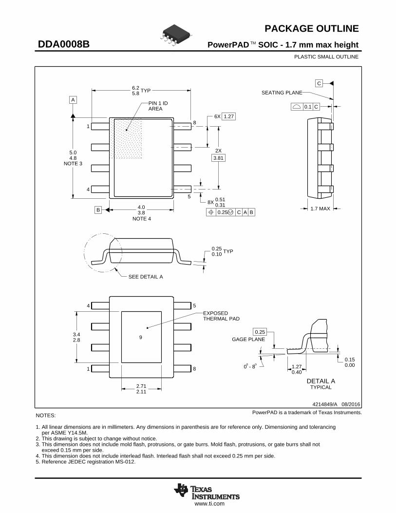
PowerPAD SOIC - 1.7 mm max heightDDA0008BPLASTIC SMALL OUTLINE
NOTES: 1. All linear dimensions are in millimeters. Any dimensions in parenthesis are for reference only. Dimensioning and tolerancing per ASME Y14.5M. 2. This drawing is subject to change without notice. 3. This dimension does not include mold flash, protrusions, or gate burrs. Mold flash, protrusions, or gate burrs shall not exceed 0.15 mm per side. 4. This dimension does not include interlead flash. Interlead flash shall not exceed 0.25 mm per side.5. Reference JEDEC registration MS-012.
PowerPAD is a trademark of Texas Instruments.
TM
18
0.25 C A B
54
PIN 1 IDAREA
NOTE 4
SEATING PLANE
0.1 C
SEE DETAIL A
DETAIL ATYPICAL
SCALE 2.400
EXPOSEDTHERMAL PAD
4
1
5
8
9
TYP6.25.8
1.7 MAX
A
NOTE 3
5.04.8
B 4.03.8

www.ti.com
EXAMPLE BOARD LAYOUT
(5.4)
(1.3) TYP
( ) TYPVIA
0.2
(R ) TYP0.05
0.07 MAXALL AROUND
0.07 MINALL AROUND
8X (1.55)
8X (0.6)
6X (1.27)
(2.95)NOTE 9
(4.9)NOTE 9
(2.71)
(3.4)SOLDER MASK
OPENING(1.3)TYP
4214849/A 08/2016
PowerPAD SOIC - 1.7 mm max heightDDA0008BPLASTIC SMALL OUTLINE
SYMM
SYMM
SEE DETAILS
LAND PATTERN EXAMPLESCALE:10X
1
4 5
8
SOLDER MASKOPENING
METAL COVEREDBY SOLDER MASK
SOLDER MASKDEFINED PAD
9
NOTES: (continued) 6. Publication IPC-7351 may have alternate designs. 7. Solder mask tolerances between and around signal pads can vary based on board fabrication site. 8. This package is designed to be soldered to a thermal pad on the board. For more information, see Texas Instruments literature numbers SLMA002 (www.ti.com/lit/slma002) and SLMA004 (www.ti.com/lit/slma004).9. Size of metal pad may vary due to creepage requirement.10. Vias are optional depending on application, refer to device data sheet. If any vias are implemented, refer to their locations shown on this view. It is recommended that vias under paste be filled, plugged or tented.
TM
METALSOLDER MASKOPENING
NON SOLDER MASKDEFINED
SOLDER MASK DETAILSPADS 1-8
OPENINGSOLDER MASK METAL UNDER
SOLDER MASK
SOLDER MASKDEFINED

www.ti.com
EXAMPLE STENCIL DESIGN
(R ) TYP0.058X (1.55)
8X (0.6)
6X (1.27)
(5.4)
(2.71)
(3.4)BASED ON
0.125 THICKSTENCIL
4214849/A 08/2016
PowerPAD SOIC - 1.7 mm max heightDDA0008BPLASTIC SMALL OUTLINE
2.29 X 2.870.1752.47 X 3.100.150
2.71 X 3.40 (SHOWN)0.1253.03 X 3.800.1
SOLDER STENCILOPENING
STENCILTHICKNESS
NOTES: (continued) 11. Laser cutting apertures with trapezoidal walls and rounded corners may offer better paste release. IPC-7525 may have alternate design recommendations. 12. Board assembly site may have different recommendations for stencil design.
TM
SOLDER PASTE EXAMPLEEXPOSED PAD
100% PRINTED SOLDER COVERAGE BY AREASCALE:10X
SYMM
SYMM
1
4 5
8
BASED ON0.125 THICK
STENCIL
BY SOLDER MASKMETAL COVERED
SEE TABLE FORDIFFERENT OPENINGSFOR OTHER STENCILTHICKNESSES
9

IMPORTANT NOTICE
Texas Instruments Incorporated (TI) reserves the right to make corrections, enhancements, improvements and other changes to itssemiconductor products and services per JESD46, latest issue, and to discontinue any product or service per JESD48, latest issue. Buyersshould obtain the latest relevant information before placing orders and should verify that such information is current and complete.TI’s published terms of sale for semiconductor products (http://www.ti.com/sc/docs/stdterms.htm) apply to the sale of packaged integratedcircuit products that TI has qualified and released to market. Additional terms may apply to the use or sale of other types of TI products andservices.Reproduction of significant portions of TI information in TI data sheets is permissible only if reproduction is without alteration and isaccompanied by all associated warranties, conditions, limitations, and notices. TI is not responsible or liable for such reproduceddocumentation. Information of third parties may be subject to additional restrictions. Resale of TI products or services with statementsdifferent from or beyond the parameters stated by TI for that product or service voids all express and any implied warranties for theassociated TI product or service and is an unfair and deceptive business practice. TI is not responsible or liable for any such statements.Buyers and others who are developing systems that incorporate TI products (collectively, “Designers”) understand and agree that Designersremain responsible for using their independent analysis, evaluation and judgment in designing their applications and that Designers havefull and exclusive responsibility to assure the safety of Designers' applications and compliance of their applications (and of all TI productsused in or for Designers’ applications) with all applicable regulations, laws and other applicable requirements. Designer represents that, withrespect to their applications, Designer has all the necessary expertise to create and implement safeguards that (1) anticipate dangerousconsequences of failures, (2) monitor failures and their consequences, and (3) lessen the likelihood of failures that might cause harm andtake appropriate actions. Designer agrees that prior to using or distributing any applications that include TI products, Designer willthoroughly test such applications and the functionality of such TI products as used in such applications.TI’s provision of technical, application or other design advice, quality characterization, reliability data or other services or information,including, but not limited to, reference designs and materials relating to evaluation modules, (collectively, “TI Resources”) are intended toassist designers who are developing applications that incorporate TI products; by downloading, accessing or using TI Resources in anyway, Designer (individually or, if Designer is acting on behalf of a company, Designer’s company) agrees to use any particular TI Resourcesolely for this purpose and subject to the terms of this Notice.TI’s provision of TI Resources does not expand or otherwise alter TI’s applicable published warranties or warranty disclaimers for TIproducts, and no additional obligations or liabilities arise from TI providing such TI Resources. TI reserves the right to make corrections,enhancements, improvements and other changes to its TI Resources. TI has not conducted any testing other than that specificallydescribed in the published documentation for a particular TI Resource.Designer is authorized to use, copy and modify any individual TI Resource only in connection with the development of applications thatinclude the TI product(s) identified in such TI Resource. NO OTHER LICENSE, EXPRESS OR IMPLIED, BY ESTOPPEL OR OTHERWISETO ANY OTHER TI INTELLECTUAL PROPERTY RIGHT, AND NO LICENSE TO ANY TECHNOLOGY OR INTELLECTUAL PROPERTYRIGHT OF TI OR ANY THIRD PARTY IS GRANTED HEREIN, including but not limited to any patent right, copyright, mask work right, orother intellectual property right relating to any combination, machine, or process in which TI products or services are used. Informationregarding or referencing third-party products or services does not constitute a license to use such products or services, or a warranty orendorsement thereof. Use of TI Resources may require a license from a third party under the patents or other intellectual property of thethird party, or a license from TI under the patents or other intellectual property of TI.TI RESOURCES ARE PROVIDED “AS IS” AND WITH ALL FAULTS. TI DISCLAIMS ALL OTHER WARRANTIES ORREPRESENTATIONS, EXPRESS OR IMPLIED, REGARDING RESOURCES OR USE THEREOF, INCLUDING BUT NOT LIMITED TOACCURACY OR COMPLETENESS, TITLE, ANY EPIDEMIC FAILURE WARRANTY AND ANY IMPLIED WARRANTIES OFMERCHANTABILITY, FITNESS FOR A PARTICULAR PURPOSE, AND NON-INFRINGEMENT OF ANY THIRD PARTY INTELLECTUALPROPERTY RIGHTS. TI SHALL NOT BE LIABLE FOR AND SHALL NOT DEFEND OR INDEMNIFY DESIGNER AGAINST ANY CLAIM,INCLUDING BUT NOT LIMITED TO ANY INFRINGEMENT CLAIM THAT RELATES TO OR IS BASED ON ANY COMBINATION OFPRODUCTS EVEN IF DESCRIBED IN TI RESOURCES OR OTHERWISE. IN NO EVENT SHALL TI BE LIABLE FOR ANY ACTUAL,DIRECT, SPECIAL, COLLATERAL, INDIRECT, PUNITIVE, INCIDENTAL, CONSEQUENTIAL OR EXEMPLARY DAMAGES INCONNECTION WITH OR ARISING OUT OF TI RESOURCES OR USE THEREOF, AND REGARDLESS OF WHETHER TI HAS BEENADVISED OF THE POSSIBILITY OF SUCH DAMAGES.Unless TI has explicitly designated an individual product as meeting the requirements of a particular industry standard (e.g., ISO/TS 16949and ISO 26262), TI is not responsible for any failure to meet such industry standard requirements.Where TI specifically promotes products as facilitating functional safety or as compliant with industry functional safety standards, suchproducts are intended to help enable customers to design and create their own applications that meet applicable functional safety standardsand requirements. Using products in an application does not by itself establish any safety features in the application. Designers mustensure compliance with safety-related requirements and standards applicable to their applications. Designer may not use any TI products inlife-critical medical equipment unless authorized officers of the parties have executed a special contract specifically governing such use.Life-critical medical equipment is medical equipment where failure of such equipment would cause serious bodily injury or death (e.g., lifesupport, pacemakers, defibrillators, heart pumps, neurostimulators, and implantables). Such equipment includes, without limitation, allmedical devices identified by the U.S. Food and Drug Administration as Class III devices and equivalent classifications outside the U.S.TI may expressly designate certain products as completing a particular qualification (e.g., Q100, Military Grade, or Enhanced Product).Designers agree that it has the necessary expertise to select the product with the appropriate qualification designation for their applicationsand that proper product selection is at Designers’ own risk. Designers are solely responsible for compliance with all legal and regulatoryrequirements in connection with such selection.Designer will fully indemnify TI and its representatives against any damages, costs, losses, and/or liabilities arising out of Designer’s non-compliance with the terms and provisions of this Notice.
Mailing Address: Texas Instruments, Post Office Box 655303, Dallas, Texas 75265Copyright © 2018, Texas Instruments Incorporated