litho today, litho tomorrow - asmlstatic today, litho tomorrow martin van den brink president &...
TRANSCRIPT

Litho today, litho tomorrow
Martin van den Brink President & Chief Technology Officer 31 October 2016

• Application trends and economics in our ecosystem are driving increasing
demand for processing power, high-speed memory, and low-cost storage,
fueling the continuation of Moore’s law
Overview
Industry trends
Strategic
priorities
• As a result, our strategic priorities are: EUV industrialization, DUV
competitiveness, leadership in Holistic lithography and EUV extension with High
NA
Lithography
Roadmap • We have underpinned our priorities with a detailed product roadmap
October 31, 2016
Public
Slide 2
• Continuation of Moore’s law will be supported by improving patterning solutions,
achieving fast yield ramp-up, to realize attractive economics
Semiconductor
impact

1900 1905 1910 1915 1920 1925 1930 1935 1940 1945 1950 1955 1960 1965 1970 1975 1980 1985 1990 1995 2000 2005 2010 2015 2020 2025 2030
The world before 1965 was already on a Moore’s like law … computing speed/€ had been doubling every 2 years for 65 years
10-4
10-2
0
102
104
106
108
1010
1012
1014
1016
Ca
lcu
latio
ns p
er
se
co
nd
pe
r $
10
00
Analytical engine
Hollerith tabulator
IBM tabulator
National ELLIS 3000
Bell Calculator model 1
Colossus
IBM SSEC
UNIVAC
IBM 704
DEC POP-1
IBM 1130
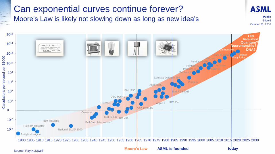
Moore’s Law Source: Ray Kurzweil
October 31, 2016
Public
Slide 3

1900 1905 1910 1915 1920 1925 1930 1935 1940 1945 1950 1955 1960 1965 1970 1975 1980 1985 1990 1995 2000 2005 2010 2015 2020 2025 2030
When ASML started Moore’s law was effective for 84 yrs
10-4
10-2
0
102
104
106
108
1010
1012
1014
1016
Ca
lcu
latio
ns p
er
se
co
nd
pe
r $
10
00
Analytical engine
Hollerith tabulator
IBM tabulator
National ELLIS 3000
Bell Calculator model 1
Colossus
IBM SSEC
UNIVAC
IBM 704
DEC POP-1
IBM 1130
DEC POP-10
Apple II IBM PC
Altair 8800
IBM AT-80266
ASML is founded Source: Ray Kurzweil
Moore’s Law
October 31, 2016
Public
Slide 4

1900 1905 1910 1915 1920 1925 1930 1935 1940 1945 1950 1955 1960 1965 1970 1975 1980 1985 1990 1995 2000 2005 2010 2015 2020 2025 2030
October 31, 2016
Slide 5
Public
Today Moore’s law is effective for 116 years
10-4
10-2
0
102
104
106
108
1010
1012
1014
1016
Ca
lcu
latio
ns p
er
se
co
nd
pe
r $
10
00
Analytical engine
Hollerith tabulator
IBM tabulator
National ELLIS 3000
Bell Calculator model 1
Colossus
IBM SSEC
UNIVAC
IBM 704
DEC POP-1
IBM 1130
DEC POP-10
Apple II IBM PC
Altair 8800
IBM AT-80266
ASML is founded Moore’s Law
Compaq Deskpro 386
Pentium
Pentium II
Pentium III
Pentium IV Core 2 duo
Core i7 quad
today
Pentium G4400
Core i3
AMD A8
Source: Ray Kurzweil
1900 1905 1910 1915 1920 1925 1930 1935 1940 1945 1950 1955 1960 1965 1970 1975 1980 1985 1990 1995 2000 2005 2010 2015 2020 2025 2030
October 31, 2016
Slide 6
Public
Can exponential curves continue forever? Moore’s Law is likely not slowing down as long as new idea’s
10-4
10-2
0
102
104
106
108
1010
1012
1014
1016
Ca
lcu
latio
ns p
er
se
co
nd
pe
r $
10
00
Analytical engine
Hollerith tabulator
IBM tabulator
National ELLIS 3000
Bell Calculator model 1
Colossus
IBM SSEC
UNIVAC
IBM 704
DEC POP-1
IBM 1130
DEC POP-10
Apple II IBM PC
Altair 8800
IBM AT-80266
ASML is founded Moore’s Law
Compaq Deskpro 386
Pentium
Pentium II
Pentium III
Pentium IV Core 2 duo
Core i7 quad
DNA?
Quantum?
today
Neuromorphic?
Pentium G4400
Core i3
AMD A8
Cannonlake
Icelake Kaby Lake
1 nm
transistors?
Source: Ray Kurzweil

October 31, 2016
Slide 7
Public
10-4
10-2
0
102
104
106
108
1010
1012
1014
1016
Ca
lcu
latio
ns p
er
se
co
nd
pe
r $
10
00
Analytical engine
Hollerith tabulator
IBM tabulator
National ELLIS 3000
Bell Calculator model 1
Colossus
IBM SSEC
UNIVAC
IBM 704
DEC POP-1
IBM 1130
DEC POP-10
Apple II IBM PC
Altair 8800
IBM AT-80266
ASML is founded Moore’s Law
Compaq Deskpro 386
Pentium
Pentium II
Pentium III
Pentium IV Core 2 duo
Core i7 quad
DNA?
Quantum?
today
Neuromorphic?
Pentium G4400
Core i3
AMD A8
Cannonlake
Icelake Kaby Lake
1 nm
transistors?
Long term multi-decade device roadmap Substantial performance gain next to the impact of geometric scaling
FPGA 2.0
Source: John Kelly III, IBM, December 2015
Ove
rall
Sys
tem
Pe
rfo
rma
nc
e
eDRAM
3D
Photonics
PCM-SCM
Base CMOS
geometric
scaling
2012 2017 2022 2032
FINFET
eMRAM
Carbon Nanotube
Neuromorphic Computing
Gate All Around
Every scaling innovation
multiplies the value provided
by our geometric scaling
Q1
Q2
Q3
Quantum Computing
1 nm transistors

Application trends in our industry drive continued demand for Moore’s Law
…drive a reinforcing cycle of data creation,
transmission, storage and processing…
Ultrafast & high-band-width
network infrastructure
Very high volumes of low-
cost semicon devices
Explosion of high-
performance storage
capacity
Massive computing power
and performance memory
in-cloud and in-vehicle
Industry trends towards 2020 and beyond
50B connected Internet of Things devices –
needing low-cost devices and generating
large data volumes requiring storage and
processing
89 million connected cars on the road of
which 6 million self-driving – generating and
processing >1 GB of data per second each
250 million personal health wearables and
connected pharmaceuticals for health data
collection
Explosion of (mostly unstructured) data,
growing to >40 Zetabytes from 5 Zetabytes
today
…driving
demand for
both low-cost
and high
performance
semiconductor
products in both
memory and
logic
…enabled by the
continuation of
Moore’s law…
…which
underpinned by
an ecosystem
with combined
profits of
>290B$
Source: McKinsey, ASML
October 31, 2016
Public
Slide 8

Geometrical scaling critical in support of Moore’s law now enabled trough 4 engines of innovations
Source: IMEC, customers
October 31, 2016
Public
Slide 9
Today’s memory architecture Future vision
DRAM
SSD
HDD
DRAM
Storage class
memory
SSD
HDD
Circuit scaling
System-on-chip and advanced packaging
Device scaling
New devices and materials
Architecture scaling
Solution optimization
Geometric scaling
2D shrink through patterning
System in Package (SiP)
Die 1
Die 2
SAW
Filter Die 4
Die 3
MFMS
Die 1
Die 2 Die 3
SAW
Filter
MFMS
Die 4
Die 3

October 31, 2016
Slide 10
Public
Logic device and shrink roadmap New devices for 5 nm and beyond are demonstrated to work
Source: IMEC
Sw
itch
ing
th
resh
old
, m
V/V
2010 2015 2020 2025
Lo
gic
Nanowire device structure
enables further reduction of
gate lengths
Scaling of devices is enabled
by materials innovation:
• High-K
• III-V
Imp
rov
ed
perf
orm
an
ce
Gate length, μm
Planar
32 nm
FinFET
14 nm
Horizontal
Nanowire
5 nm
Vertical
Nanowire
~2.5 nm ~ 1 nm
>2025
One nanometer
transistor, UC Berkeley

October 31, 2016
Slide 11
Public
Large innovation ongoing in memory, driving continued litho demand
1ms
1 µs
1ns
Ac
ce
ss
tim
e
0.01 0. 1 1 10
NAND
DRAM
STT-MRAM
Storage
Storage-class
memory
Working
memory
Cost ($/GB)
X-Point
Hard disk
drive
Non-volatile
Volatile
SRAM
Source: Western Digital
NAND displacing hard disks,
3D NAND displacing 2D NAND,
significant integration challenges
Storage class
memory filling gap
between working
memory and storage
1 Alternative technologies (e.g., CBRAM, PCRAM) likely high litho volume and performance
DRAM
challenges in
shrink and cost
reduction

October 31, 2016
Public
Slide 12
Solid state replacing high performance disk memory And new memory technologies to drive the overall performance
Source: Will Akin, Micron, Short Course, IEEE IMW may 2016
Rela
tive d
ata
volu
me

EUV could simplify customers’ patterning process
Resolution
Top view
Lithography
Deposition
Etch
Cross section view
pitch
Spacer process makes 1D
grids with high resolution
Top view
Litho-etch process makes 2D
patterns
Final pattern
Note: process schematics are simplified for presentation purposes litho critical
dimension
Litho critical dimension / 2n Litho critical dimension / √n
litho hard mask
spacer deposition
etch 1 etch 2 strip
Litho step 1
Litho step 2
Etch step 1
Etch step 2
October 31, 2016
Public
Slide 13

Edge placement error (EPE) and litho critical
dimension (CD) main patterning parameters…
node x node x+2
…and shrink requires ever tighter
requirements
Intended cut
CD uniformity
error
Overlay
error
Edge placement error
(EPE): combined error
of overlay and CD
uniformity
Same resolution
not sufficient
Same EPE at
lower resolution
not sufficient
Smaller litho
critical dimension
needed
Better EPE
performance
needed (overlay
and CD control)
Smaller litho
critical dimension
needed Litho
critical
dimension
Edge placement error & litho critical dimension challenges are main factors for continued shrink
October 31, 2016
Public
Slide 14

Source: ASML
Litho etch (LEx)
Single expose (SE)
Customer perspective
Cost
EPE
complexity
Process
complexity
-
October 31, 2016
Public
Slide 15
Single Exposure lithography is most attractive optimizing cost, cycle time, yield and edge placement challenges
~ ~ ~

EUV Production
Insertion Window
2014 2015 2016 2017 2018 2019 2020 2021 2022
>x200 >x192 >x128
Planar Floating Gate NAND
>x96
Sto
rag
e
Me
mo
ry 14-15
3D NAND
x64
17-18 22
x48 x32 x24
October 31, 2016
Slide 16
Public
Industry Shrink Roadmap & EUV insertion
HVM
Production1
Research1
Development1
Roadmap2
Today’s status
x number of layers
3nm 5nm 7nm 10nm 16-14nm 20nm Lo
gic
P
erf
orm
an
ce
Me
mo
ry
Public
Slide 16
Source: 1) Customers - public statements, IC Knowledge LLC; 2) ASML extrapolations
Sto
rag
e
Cla
ss
Me
mo
ry
next 1Z 1Y 1X 20-22 28-30
DRAM
1Z”/x8 1Y”/x8
PC-RAM, ReRAM, X-point etc.
1X”/x4 2X’/x2
Node name
Minimum half pitch
Minimum half pitch
/x number of layers

Strategic priorities to meet customer requirements Grow our Litho business by delivering superior customer value
Holistic
Litho
• Build a winning position in Pattern Fidelity Control leveraging inspection
combined with superior computational Litho
EUV
extension
• Deliver High-NA EUV in time to support customer roadmaps and avoid
complex and costly alternatives
DUV
competitiveness
• Drive DUV performance ‒ Continue to lead in innovation
‒ Drive operational excellence
‒ Expand installed base business
EUV
industrialization
• Deliver high volume manufacturing performance metrics
• Enhance EUV value for future nodes
October 31, 2016
Public
Slide 17
1
2
3
4
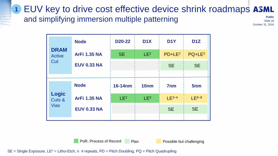
Possible but challenging Plan
Node
ArFi 1.35 NA Logic Cuts &
Vias
16-14nm 5nm 7nm 10nm
LE2 LE6~8 LE3~4 LE3
DRAM Active
Cut
ArFi 1.35 NA
Node
LE2 PD+LE2
D1X
D1Z D1Y D20-22
PQ+LE2
EUV 0.33 NA
EUV 0.33 NA SE SE
SE = Single Exposure, LEn = Litho-Etch, n # repeats, PD = Pitch Doubling, PQ = Pitch Quadrupling
PoR, Process of Record
SE
SE SE
EUV key to drive cost effective device shrink roadmaps and simplifying immersion multiple patterning
October 31, 2016
Public
Slide 18
1

October 31, 2016
Slide 19
Public
EUV industrialization: productivity and consistency >1500 wafers per day at customer fab, variability needs improvement
0
200
400
600
800
1000
1200
1400
1600
1800
day 1 day 2 day 3
Pro
du
ctivity [
wp
d]
• Source: NXE:3350B
• Each bar represents customer wafers exposed on
one individual day
3 day average 1,500 wafer per day at customer site
Source: Britt Turkot, Intel, 2016 international symposium on EUV, 24 October 2016, Hiroshima
Source: TSMC, Semicon Taiwan, Sep 2016
System average availability at customer site
1

October 31, 2016
Slide 20
Public
We will deliver continued reliability improvement and ramp up our operations to realize EUV in volume manufacturing
Source: ASML, public statements
EUV will drive costs and process complexity down for
our customers
50%
All ArFi
34%
With EUV
1,743
-30%
2,505
Litho CapEx Opex
Non-litho CapEx
Patterning cost per wafer 5nm, €
… and has made good progress in productivity and reliability
2016
Target:
1,500
2016
YtD
2014
>1,500
>500
2015
>1,000
… triggering increased customer demand
51 55
80
2015 2016 YTD
2016
Target:
80%
2014
“We plan to extensively use EUV in 5nm to
improve density, simplify process complexity,
and reduce cost…Recently EUV development
gained quite a good momentum across the
industry. ”
Mark Liu, co-CEO TSMC, July ‘16
“Samsung fully intends to deploy EUV for
7nm, triple patterning is not viable …”
“We expect production in 2018”
AnandTech & SemiconWest ‘16
“Significant strides have been made … taking
the technology from a question of if to a
question of when. EUV is solidly on a path
to HVM insertion as soon as the technology
becomes ready and cost effective”
Intel, SPIE ‘16
Productivity
Wafers/day at customer site
Reliability
%, max avg 4 wk availability of
installed base
1
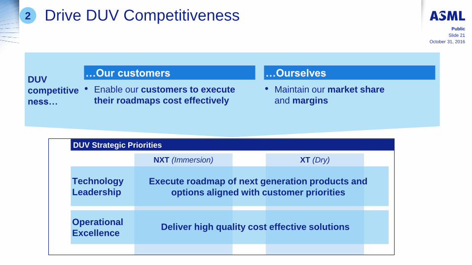
Drive DUV Competitiveness
October 31, 2016
Public
Slide 21
XT (Dry)
DUV Strategic Priorities
NXT (Immersion)
Technology
Leadership
Operational
Excellence
Execute roadmap of next generation products and
options aligned with customer priorities
Deliver high quality cost effective solutions
• Maintain our market share
and margins
DUV
competitive
ness…
• Enable our customers to execute
their roadmaps cost effectively
…Our customers …Ourselves
2

Overlay [nm]
October 31, 2016
Slide 22
Public
TWINSCAN Immersion system roadmap
>285 WpH 190 WpH 230 WpH 275 WpH 250 WpH
NXT:1950i
NXT:1960Bi NXT:1965Ci
NXT:1970Ci
NXT:1980Di
NXT:next1
NXT:next2
products under study
2013
2015
2011
2009
introduction
Roadmap: October 2016
7
6
4
3
<3
<2
2

Next slides
Improvements on Next Generation products Overlay, DUV to EUV matching
October 31, 2016
Public
Slide 23
Process robust Alignment
improves overlay performance
Process robust Leveling
Improves machine matching
Wafer Handler
Improves overlay performance
Projection Lens
Optimization of lens for improved
imaging and overlay
Improved Grid Setup
Improved overlay and machine
matching
Wafer heating control
Improved overlay performance
Wafer table
Improved machine matching
Overlay - general Imaging/Focus
2

Alignment process robustness improvement Using multiple wavelengths & polarizations; applicable for DUV and EUV
30 different process
stacks and marker
combinations in
both FEOL and
BEOL
carbon
Si wafer
BARC
resist
ILD
“poly”
ILD copper ILD ILD
copper copper ILD
5x process
excursion reduction
2x process
robustness reduction
Current alignment
sensor
+ 2 polarizations and improved
algorithms
+ intensity information
improved algorithms
Color weighting Best Color
Measured Overlay
11.6 nm, 7.5 nm Measured Overlay
6.7 nm, 6.14 nm
Using existing
sensor at 0º and
90º wafer rotations
2
October 31, 2016
Public
Slide 24

Improved focus and leveling process robustness
Through optimized spectrum & angle of incidence; applicable to DUV & EUV
wafer wafer
resist BARC
hardmask
Product layer
Silicon substrate
70°
offset
Hard mask thickness [nm]
resist BARC
hardmask
Product layer
Silicon substrate
>70°
offset
Spectrum
improvement
Lig
ht
inte
nsit
y [
a.u
.]
7 different customer process layers Pro
ce
ss d
ep
en
de
nt
foc
us o
ffse
t Current version New version
Current version
New version
Current version New version
October 31, 2016
Public
Slide 25
2

October 31, 2016
Slide 26
Public
TWINSCAN Dry system roadmap Continued improvements in productivity and capability of all 4 product lines
Roadmap: October 2016
210 WpH 220 WpH 225 WpH 230 WpH 240 WpH 178-185 205 WpH
20nm
Overlay
7nm
14nm
10nm
60nm
XT:860K
TOP
TOP
XT:860L
TOP
XT:400K
TOP
XT:400L
TOP
9nm
5nm
6nm
XT:400H
365 nm
XT:1460K
XT:1000H
248 nm
XT:860H
248 nm
TOP
PEP
TOP
XT:1060K
XT:860M
TOP
XT:1450H
193 nm
PEP PEP PEP
PEP PEP
XT:1450
ArF
XT:1000
High NA KrF
XT:860
KrF
XT:400
I-line
TOP Overlay improvement PEP Productivity improvement
2

ASML Holistic Lithography integrates 3 competences Resulting in 3 customer value propositions
Process Window Detection Computational
Lithography Metrology
Other patterning tools
2
1
3
6
Process Window
Control Stepper control through on-
product overlay, focus and
pattern fidelity feedback loops.
5 Process Window
Enhancement
Stepper set up and
layout optimization
for maximum process
window
4
Lithography scanner with advanced control capability
(imaging, overlay and focus)
Metrology process robust target
and recipe creation, ebeam
model calibration and
computational guided detection.
October 31, 2016
Public
Slide 27
3

YieldStar: Unique on product overlay metrology measuring overlay of actual device features, DRAM example
Yie
ldsta
r C
D-S
EM
October 31, 2016
Public
Slide 28
3.2

Customer‘s patterns
Model error (simulated CD – wafer CD) comparison
between empirical NTD model and physical resist shrinkage model
Representative
2D patterns
Mo
de
l e
rro
r X
0
1D patterns
Unique Negative Tone resist modelling capability Modelling accuracy improved 60%
NTD: the same features are printed in positive resist using light-field masks, with consequently
better image contrast; with NTD the exposed resist areas remain intact.
However, this approach involves additional processing steps (typically coating, baking, etching)
and the exposed area is affected in 3 dimensional ways (see open arrows)
Empirical NTD resist
model does not capture
3 dimensional shrink
impact
Physical NTD resist
model accounts for 3
dimensional shrink
impacting 2D OPC
accuracy
October 31, 2016
Public
Slide 29
3.3

ASML holistic lithography at 1x nm node: Overlay Control
Computational Lithography
After Litho YieldStar
Metrology
Scanner Control
1
3
2
Pre-Holistic Lithography Holistic Lithography
October 31, 2016
Public
Slide 30
3

ASML holistic lithography future - Pattern fidelity control
Computational Lithography
Scanner Control
1 2 After Litho / Etch
E-beam Metrology
Guide to areas of interest
2 2 Scanner
metrology (100% wafers)
Improved models
October 31, 2016
Public
Slide 31
3
After Litho YieldStar
Metrology
3

ASML holistic lithography future: Pattern fidelity control:
reducing pattern errors up to~ 50%
and reduce
pattern error by
~50% by control
Focus map CD map
Hot spots
Pattern error prediction
Pattern error
measurement Hotspot count →
Err
or
count→
Uncontrolled
Controlled
October 31, 2016
Public
Slide 32
3
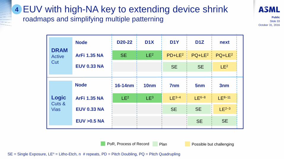
Possible but challenging Plan
Node
ArFi 1.35 NA Logic Cuts &
Vias
16-14nm 3nm 5nm 7nm 10nm
LE2 LE8~11 LE6~8 LE3~4 LE3
DRAM Active
Cut
ArFi 1.35 NA
Node
LE2 PD+LE2
D1X
next D1Z
D1Y D20-22
PQ+LE2 PQ+LE2
EUV >0.5 NA
EUV 0.33 NA
SE
LE2~3
EUV 0.33 NA SE SE
SE = Single Exposure, LEn = Litho-Etch, n # repeats, PD = Pitch Doubling, PQ = Pitch Quadrupling
SE
PoR, Process of Record
SE
LE2
SE SE
EUV with high-NA key to extending device shrink roadmaps and simplifying multiple patterning
4
October 31, 2016
Public
Slide 33

High NA delivers value to our customers through process simplification, patterning cost and further shrink
# of passes, <5 nm node
• Faster yield-roadmap
• Faster cycle time
• Easier node transition
… it reduces patterning cost1
Patterning cost per layer, EUR
… and delivers continuation
of shrink roadmap
92
62
No high
NA
-33%
With High
NA
0.33 double
patterning
0.55 single
exposure
-42%
Litho
Non-Litho
Source: ASML
1 SE = single exposure, LE2 = double patterning;
2015 2020 2025 2030
HVM of node, years
1.4 nm
2 nm
3 nm
5 nm
7 nm
10 nm 100%
10%
1%
High NA No High NA
Relative cost per function, %
High NA simplifies
process technology
October 31, 2016
Public
Slide 34
4

Source: Zeiss, “EUV lithography optics for sub-9nm resolution,” Proc. SPIE 9422, (2015).
October 31, 2016
Slide 35
Public
High-NA optics design concepts available Larger elements with tighter specifications
NA 0.25 NA 0.33 NA >0.5 Design examples
Wafer
level
Reticle
level
Extreme aspheres enabling
further improved wavefront /
imaging performance
Big last mirror driven by
High NA
Tight surface specifications enabling
low straylight / high contrast imaging
Obscuration enables
higher optics transmission
Potential of up to 2x vs 3300
4

Anamorphic High NA EUV reduces the angles enabling a solution with 26 mm slit on 6” masks
@ wafer @ reticle Projection with 0.33 NA
Mag X: 4x Mag Y: 4x
QF
10
4 m
m
132 mm
x
y 6‘‘
26 mm
33 mm
Reticle layout compatible with
today 6” mask production
October 31, 2016
Public
Slide 36
Source: Jan van Schoot, ASML, “EUV roadmap extension by higher Numerical Aperture”, 2016 international symposium on EUV, 24 October 2016, Hiroshima
4

Anamorphic High NA EUV reduces the angles enabling a solution with 26 mm slit on 6” masks
@ wafer @ reticle
Projection with >0.5 NA Mag X: 4x Mag Y: 4x
x
y 6‘‘
October 31, 2016
Public
Slide 37
QF
26 mm
33 mm
Reticle layout compatible with
today 6” mask production
Source: Jan van Schoot, ASML, “EUV roadmap extension by higher Numerical Aperture”, 2016 international symposium on EUV, 24 October 2016, Hiroshima
10
4 m
m
132 mm
4

Anamorphic High NA EUV reduces the angles enabling a solution with 26 mm slit on 6” masks
@ wafer @ reticle
Projection with >0.5 NA Mag X: 4x Mag Y: 8x
QF
x
y 6‘‘
26 mm
16.5 mm
October 31, 2016
Public
Slide 38
Reticle layout compatible with
today 6” mask production
Source: Jan van Schoot, ASML, “EUV roadmap extension by higher Numerical Aperture”, 2016 international symposium on EUV, 24 October 2016, Hiroshima
10
4 m
m
132 mm
4

October 31, 2016
Slide 39
Public
Anamorphic optics are used in cinematography
Anamorphic
Lens Anamorphic
Projector
“The Mask”
(24x36mm2)
16x9 16x9
“Don’t change the mask”
4

High-NA delivers higher throughput
Source: ASML
50
200
100
150
0
15 10 25 20 5 0
+25%
W*cm2/mJ
0.33NA High NA
anamorphic
At any power / dose, High NA delivers
higher throughput than 0.33NA due to:
Higher lens transmission
Improved stage speeds
High-NA vs. 0.33NA throughput at given dose
250W – 20mJ/cm2
Full
Field
October 31, 2016
Public
Slide 40
Th
rou
gp
hut (w
afe
rs/h
ou
r)
Half
Field
4

Overlay [nm] 55 WPH 125 WPH 185 WPH 145 WPH
NXE:3300B
NXE:3350B
NXE:next
High NA
October 31, 2016
Slide 41
Public
EUV extension roadmap
NXE:3400B 2017
2015
2013
Roadmap: October 2016
introduction
products under study
7
3.5
3
<3
<2
4

October 31, 2016
Slide 42
Public
The future
• Moore’s law to continue for the foreseeable future, driven by connecting
everything around us, generating massive data and enabled by geometrical
device, architectural and circuit scaling. Logic device innovation and
memory/computer architecture innovations in support of this.
• EUV industrialization enabled by identified insertion opportunity at multiple
customers and execution to roadmaps progressing to plan, improvements still
needed for consistency.
• DUV competitiveness to support continued demand given its cost advantage
over EUV for less critical layers and some double patterning. Improvements in CD
and overlay continued to be required for future nodes.
• Holistic Lithography is being extended with pattern fidelity control. Metrology
extensions needed for on product robust process, after etch targets and resolution
enhancements through computational enhanced e-beam capability. Increased
scanner control capability to enable ultimate on product process control.
• EUV extension with high NA enable cost-effective shrink to continue into the next
decade

October 31, 2016
Slide 43
Public
Forward looking statements This document contains statements relating to certain projections and business trends that are forward-looking, including statements with respect to our outlook,
including expected customer demand in specified market segments (and underlying assumptions) including memory, logic and foundry, expected sales levels, trends,
including trends towards 2020 and beyond and expected industry growth, and outlook, systems backlog, expected or indicative market opportunity, financial results and
targets, including, for ASML and ASML and HMI combined, expected sales, other income, gross margin, R&D and SG&A expenses, capital expenditures, cash
conversion cycle, EPS and effective annualized tax rate, annual revenue opportunity and EPS potential by end of decade and growth opportunity beyond 2020 for
ASML and ASML and HMI combined, cost per function reduction and ASML system ASP, goals relating to gross cash balance and ASML’s capital structure, customer,
partner and industry roadmaps, productivity of our tools and systems performance, including EUV system performance (such as endurance tests), expected industry
trends and expected trends in the business environment, the addition of value through delivery of lithography products and the achievement of cost-effective shrink,
expected continued lithography demand and increasing lithography spend, the main drivers of lithography systems, lithography intensity for all market segments,
customer execution of shrink roadmaps, future memory application distribution, expected addressable markets, including the market for lithography systems and service
and options, expected manufacturing and process R&D, statements with respect to growing end markets that require fab capacity driving demand for ASML’s tools,
statements with respect to the acquisition of HMI by ASML, including market opportunity, the expected timing of completion of the HMI acquisition and delisting of HMI,
the expected benefits of the acquisition of HMI by ASML, including expected continuation of year on year growth, the provision of e-beam metrology capability and its
effect on holistic lithography solutions, including the introduction of a new class of pattern fidelity control and the improvement of customers’ control strategy, statements
with respect to EUV, including targets, such as availability, productivity, facilities and shipments, including the number of EUV systems expected to be shipped and
timing of shipments, and roadmaps, shrink being key driver to industry growth, expected industry adoption of EUV and statements with respect to plans of customers to
insert EUV into production and timing, the benefits of EUV, including expected cost reduction and cost-effective shrink, the expected continuation of Moore's law,
without slowing down, and that EUV will continue to enable Moore’s law and drive long term value, goals for holistic lithography, including pattern fidelity control,
expectations relating to double patterning, immersion and dry systems, intention to return excess cash to shareholders, statements about our proposed dividend,
dividend policy and intention to repurchase shares and statements with respect to the current share repurchase plan. You can generally identify these statements by the
use of words like "may", "will", "could", "should", "project", "believe", "anticipate", "expect", "plan", "estimate", "forecast", "potential", "intend", "continue" and variations of
these words or comparable words. These statements are not historical facts, but rather are based on current expectations, estimates, assumptions and projections
about the business and our future financial results and readers should not place undue reliance on them.
Forward-looking statements do not guarantee future performance and involve risks and uncertainties. These risks and uncertainties include, without limitation, economic
conditions, product demand and semiconductor equipment industry capacity, worldwide demand and manufacturing capacity utilization for semiconductors (the principal
product of our customer base), including the impact of general economic conditions on consumer confidence and demand for our customers' products, competitive
products and pricing, the impact of any manufacturing efficiencies and capacity constraints, performance of our systems, the continuing success of technology
advances and the related pace of new product development and customer acceptance of new products including EUV, the number and timing of EUV systems
expected to be shipped and recognized in revenue, delays in EUV systems production and development, our ability to enforce patents and protect intellectual property
rights, the risk of intellectual property litigation, availability of raw materials and critical manufacturing equipment, trade environment, changes in exchange rates,
changes in tax rates, available cash and liquidity, our ability to refinance our indebtedness, distributable reserves for dividend payments and share repurchases and
timing of resumption of the share repurchase plan, and other risks indicated in the risk factors included in ASML's Annual Report on Form 20-F and other filings with the
US Securities and Exchange Commission. These forward-looking statements are made only as of the date of this document. We do not undertake to update or revise
the forward-looking statements, whether as a result of new information, future events or otherwise.
