linpak, a new low inductive phase-leg igbt module with ... · pdf filelinpak, a new low...
TRANSCRIPT
LinPak, a new low inductive phase-leg IGBT module with easy paralleling for high power density converter designs
Raffael Schnell, Samuel Hartmann, Dominik Trüssel, Fabian Fischer, Andreas Baschnagel, Munaf Rahimo, ABB Switzerland Ltd, Semiconductors, Fabrikstrasse 3, CH – 5600 Lenzburg, Switzerland, email: [email protected]
The Power Point Presentation will be available after the conference.
Abstract
In this paper, we present for the first time the LinPak, a new open standard IGBT module topology. The new phase-leg type module concept will be introduced first with a rating of 1700V and 2x1000A on a footprint of 100 x 140mm2 setting a new standard in power density. The proposed module though is designed to accommodate 1200V up to 3300V chip-sets and a 3300V version will follow soon after the presentation of the 1700V module. The new module features an exceptionally low stray inductance enabling the full utilization of advanced low switching loss IGBT chip-sets and even future full silicon carbide switch solutions. In addition the design is made for parallel connection with negligible de-rating in mind, thus a large range of inverter power can be realized with just one module type. Together with the open standard concept this module fulfills a long wish of the industry in nearly all high power segments such as traction/CAV, wind-power/solar and industrial drives to name a few.
1. Introduction Present IGBT module solutions are at its limit when it comes to advanced and faster IGBT/diode chip-sets since the overall stray inductance per switched ampere is too large and high over-voltage will occur [1]. Also the available electrical contact area of today’s modules is limited and dates back to times when the packages were rated with 50% less current than now. Due to today’s modules lack of scalability, a large variation of outlines exist to match various inverter ratings. The presented LinPak module concept addresses all these issues and is published as an open standard, meaning module manufacturers can freely adopt the outline and customers benefit from a standard solution provided by more than one supplier making inverter designs easier. The LinPak offers as well exceptional low stray inductance of 10nH and an easy customer interface enabling the construction of a very low inductive dc-connection with sufficient contact area for the high current densities. This is the ideal fit for the full utilization of the advanced fast IGBT/diode chip sets such as the latest 1700V SPT++ technology [2]. It also makes the package fit for future hybrid and full SiC solutions that come with much higher switching speeds. Beside the very advanced and novel package concept, the LinPak features ultra-sonic welded terminals and an advanced high reliability solder joint between the unrivaled AlN substrate and AlSiC base-plate material combination. Also the well established high temperature cycling capable bonding technique and the gate-print to substrate aluminum bond interconnect from the improved HiPak are incorporated in the new LinPak design.
PCIM Europe 2015, 19 – 21 May 2015, Nuremberg, Germany
ISBN 978-3-8007-3924-0 © VDE VERLAG GMBH · Berlin · Offenbach224
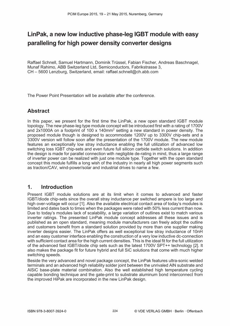
2. Application benefits 2.1. Module scalability and record current density With the LinPak just one module type per voltage rating is needed. Thanks to a homogenous current path concept, the module enables parallel connection of more than four modules without any significant de-rating.
Figure 1: LinPak scalability. The current density of LinPak modules offers a solid improvement of more than 10% compared to older module types on the market as shown in Table 1: Module Type Current Rating Foot-print Current / Area LinPak 2 x 1000A 100 x 140mm2 14.3Acm-2 HiPak 3600A 140 x 190mm2 13.5Acm-2 PrimePack 2 x 1400A 89 x 250mm2 12.6Acm-2
Table 1: Current density of LinPak compared to other module types.
2.2. Mechanical concept and connections The gate-unit connection for the LinPak is realized with a simple adapter-board (PCB) directly mounted onto the module between AC and DC terminals. The connection to the auxiliary terminals for gate, emitter, collector and thermistor are realized with M3 screws. In addition four molded M3 nuts are positioned in the corners to mechanically fix the adapter board in harsh environments like traction/CAV applications. The adapter-board connects the modules gates and aux emitters in parallel together. Thus just one gate-unit is needed independent how many modules are connected in parallel. The power connections are designed to enable an absolute symmetrical DC connection crucial for excellent current sharing. The creepage and clearance distance are designed according IEC 60664-1 and EN 50124-1 for functional insulation up to a device rating of 3300V.
2x4000A, 400 x 140mm2
2x1000A 100 x 140mm2
2x3000A 300 x 140mm2
2x2000A 200 x 140mm2
PCIM Europe 2015, 19 – 21 May 2015, Nuremberg, Germany
ISBN 978-3-8007-3924-0 © VDE VERLAG GMBH · Berlin · Offenbach225

Power connections The LinPak offers the highest contact area per rated current. Table 2 compares the current per M8 screw for various packages. For comparison of the various packages the phase current is calculated with the device nominal current divided by square root of 2: Module Type Nominal
Current Phase
Current Amp / M8
screw Phase Amp / M8 screw DC
LinPak 1000A 707A 354A 250A PrimePack 1400A 989A 495A 350A HiPak 3600A 2546A 600A 600A
Table 2: Current per M8 screw connection. As a result of the high contact area offered by the LinPak, the heating of the contact interface and as well of the terminal itself is much reduced compared to HiPak or PrimePack modules.
2.3. Record low stray inductance Present module designs have rather high stray inductance values and high over-voltages will be the result, making the use of advanced fast chip-sets such as the ABB 1700V SPT++ difficult, not even talking about very fast future SiC solutions. The LinPak design offers the lowest internal stray inductance times current and is made with the interfaces in mind, especially to enable a low inductive bus bar. In figure 2 the LinPak is compared to a HiPak including a bus bar and an assumed DC-capacitor inductance of 1.5nH. Even when including the bus bar and capacitor the over-voltage even with fast chip-sets is below critical levels compared to the HiPak solution. This makes the LinPak the ideal candidate for parallel connection up to high current applications without compromising the switching losses.
Figure 2: Stray inductance including bus bar.
HiPak (1.7 kV / 3600A) 4 LinPak (1.7 kV / 4000A)
Module inductance 16nH 2.5nH (10nH for a single module)
Bus-bar inductance 10nH 1.5nH
Capacitor inductance 1.5nH 1.5nH
Total (module including DC-link) 27.5nH 5.5nH(22nH for a single module)
Lσ ∙ Inom (3600A) 99μVs 19.8μVs
Over-voltage @tf = 0.12μs (1700V SPT++)
825V100%
165V20%
PCIM Europe 2015, 19 – 21 May 2015, Nuremberg, Germany
ISBN 978-3-8007-3924-0 © VDE VERLAG GMBH · Berlin · Offenbach226

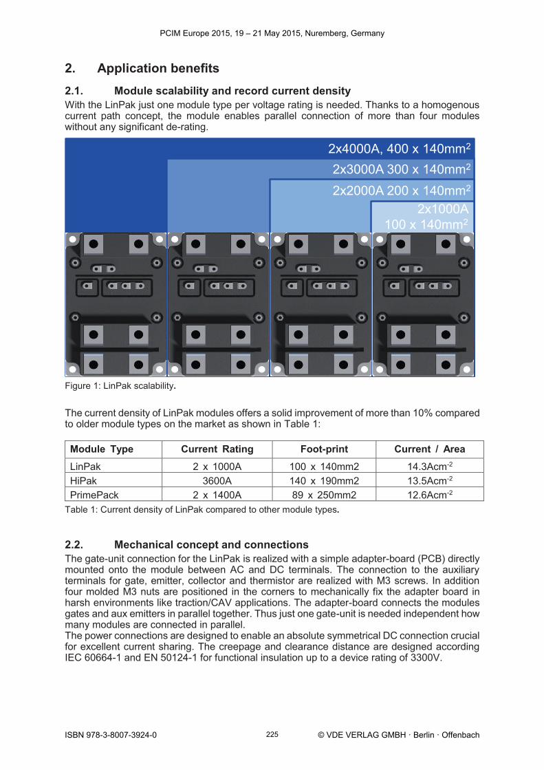
3. Electromagnetic simulations In order to verify the electrical module design with respect to internal current sharing and to get a first impression of the parasitic inductance and coupling values, electro-magnetic finite element simulations have been done for the LinPak demonstrator as well as for an improved 2nd learning cycle LinPak design. The models include all the conductors of the module and the bus bar as used for the measurements and a cooler. The conductors are placed within a volume of about 300 mm in diameter and the whole volume is meshed. The bottom side of the cooler and the DC- bus bar were connected to ground. A 100kHz AC current is fed to the DC+ bus bar. For the commutation from the low side diode to the high side IGBT, the high side IGBTs and the low side diodes are modelled as a resistive material with a total resistance of 0.01Ω. This results in 10V resistive voltage drop per switch with an equal current sharing between the chips. The other commutation case is modelled accordingly. The outer gate and emitter contacts of the module are short circuited and the voltage between gate and emitter on each chip’s metallization is recorded. From the imaginary part of this voltage, the inductive coupling of the commutation loop current into the power circuit and the control circuit can be estimated. This is illustrated in figures 3 and 4. The result of the simulation is shown in figure 5 as the distortion voltage obtained when switching the module’s nominal current e.g. 1000A within 250ns. The first learning cycle showed the low side switch of the demonstrator to be slightly stronger damped than the high side switch. Also the simulation indicates some current imbalance between the chips. For the improved design of the 2nd learning cycle the balance is improved by having a better symmetry in the load conductor path. The module stray inductance obtained from the simulation is shown in figure 6. The main contributor are the power terminals. From the 1st learning cycle with 15.7nH, an improvement is achieved resulting in 12.5nH for the 2nd learning cycle. Overall the simulation results match well with the measurement where we achieve a module stray inductance of about 10nH.
Figure 3&4: Imaginary part of the potential divided by di/dt, which corresponds to nH of induction. The damping of the gate to emitter signal is clearly visible (right).
PCIM Europe 2015, 19 – 21 May 2015, Nuremberg, Germany
ISBN 978-3-8007-3924-0 © VDE VERLAG GMBH · Berlin · Offenbach227
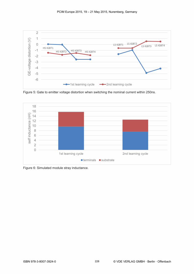
Figure 5: Gate to emitter voltage distortion when switching the nominal current within 250ns.
Figure 6: Simulated module stray inductance.
HS IGBT1HS IGBT2 HS IGBT3 HS IGBT4
LS IGBT1 LS IGBT2LS IGBT3 LS IGBT4
-6
-5
-4
-3
-2
-1
0
1
2G
E-vo
ltage
dis
torti
on (V
)
1st learning cycle 2nd learning cycle
02468
1012141618
1st learning cycle 2nd learning cycle
self
indu
ctan
ce (n
H)
terminals substrate
PCIM Europe 2015, 19 – 21 May 2015, Nuremberg, Germany
ISBN 978-3-8007-3924-0 © VDE VERLAG GMBH · Berlin · Offenbach228
4. Electrical measurements of prototype modules Prototype modules with a current rating of 2x900A have been tested in a double pulse test setup at a realistic customer DC-link with laminated bus bars specifically designed for the new LinPak (fig. 7).
Figure 7: Double pulse test setup. The measurements fully confirmed the expectations in the LinPak concept. The tests revealed that an overall DC-link stray inductance including module, bus bar and capacitors of about 25nH can be achieved already with the prototype module. As a result, the over-voltage from the switching stays well within the maximum device rating and snappy diode recovery can be considered as a term of the past. Figures 8 to 10 show the switching waveforms at nominal conditions while figure 11 shows the device under test. The switching characteristics are very smooth and without any oscillations. The modules have as well been tested up to the specified Safe Operating Area, thanks to the low stray inductance no active clamp was needed to limit the IGBT over-voltage and both, IGBT and Diode SOA show very clean waveforms (fig 12&13). In addition the low- and high-side switch show very similar characteristics where the darker colours show the low-side switch.
PCIM Europe 2015, 19 – 21 May 2015, Nuremberg, Germany
ISBN 978-3-8007-3924-0 © VDE VERLAG GMBH · Berlin · Offenbach229
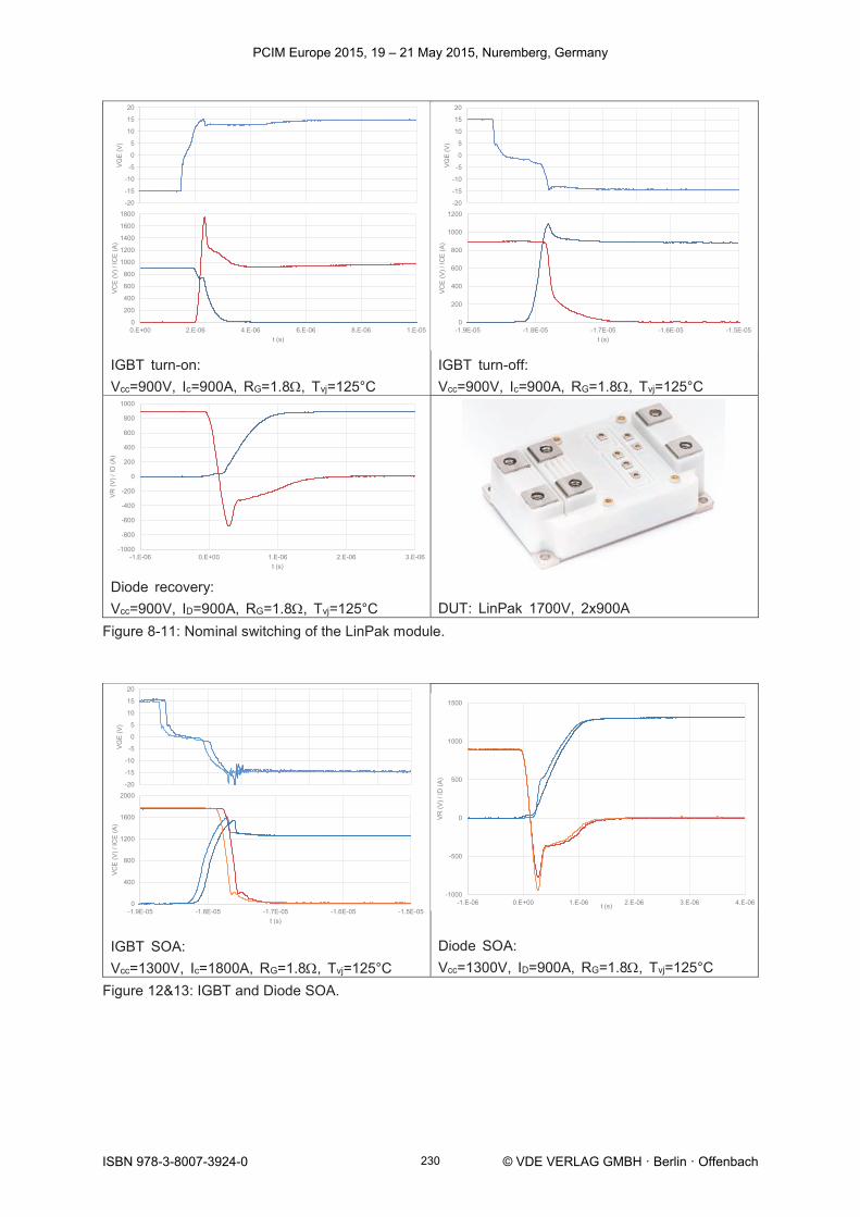
IGBT turn-on: Vcc=900V, Ic=900A, RG=1.8 , Tvj=125°C
IGBT turn-off: Vcc=900V, Ic=900A, RG=1.8 , Tvj=125°C
Diode recovery: Vcc=900V, ID=900A, RG=1.8 , Tvj=125°C
DUT: LinPak 1700V, 2x900A
Figure 8-11: Nominal switching of the LinPak module.
IGBT SOA: Vcc=1300V, Ic=1800A, RG=1.8 , Tvj=125°C
Diode SOA: Vcc=1300V, ID=900A, RG=1.8 , Tvj=125°C
Figure 12&13: IGBT and Diode SOA.
0
200
400
600
800
1000
1200
1400
1600
1800
0.E+00 2.E-06 4.E-06 6.E-06 8.E-06 1.E-05
VCE
(V) /
ICE
(A)
t (s)
-20
-15
-10
-5
0
5
10
15
20VG
E (V
)
0
200
400
600
800
1000
1200
-1.9E-05 -1.8E-05 -1.7E-05 -1.6E-05 -1.5E-05
VCE
(V) /
ICE
(A)
t (s)
-20
-15
-10
-5
0
5
10
15
20
VGE
(V)
-1000
-800
-600
-400
-200
0
200
400
600
800
1000
-1.E-06 0.E+00 1.E-06 2.E-06 3.E-06
VR (V
) / ID
(A)
t (s)
0
400
800
1200
1600
2000
-1.9E-05 -1.8E-05 -1.7E-05 -1.6E-05 -1.5E-05
VCE
(V) /
ICE
(A)
t (s)
-20
-15
-10
-5
0
5
10
15
20
VGE
(V)
-1000
-500
0
500
1000
1500
-1.E-06 0.E+00 1.E-06 2.E-06 3.E-06 4.E-06
VR (V
) / ID
(A)
t (s)
PCIM Europe 2015, 19 – 21 May 2015, Nuremberg, Germany
ISBN 978-3-8007-3924-0 © VDE VERLAG GMBH · Berlin · Offenbach230

5. Conclusions & Outlook The LinPak is a new open standard module concept that satisfies the requirements posed both by new advanced fast and high current density chip-sets, but as well from customers wishing a flexible and scalable solution, which is also ready for future technologies such as SiC devices. In this paper we have shown the benefits of the novel low stray inductance LinPak. Simulations as well as measurements have confirmed the expectations into the new package. Status and Outlook: Today, the benefits of the new package enable the customer to profit from the latest chip technologies with low inductance for achieving the highest current density. Furthermore, particle free ultrasonic welding of the main terminals, advanced wire bonding including the well-established and unrivaled AlN / AlSiC substrate / baseplate material combination for high temperature cycling capability are incorporated. Looking ahead, the new module also allows a smooth phase-in of future technologies both on chip level with respect to silicon and SiC based devices as well as on advanced material joining techniques as they become available for cost efficient mass production without major changes in the converter design.
6. References 1. Raffael Schnell, Munaf Rahimo “The Quest for Higher Switching Frequency and its
Implications on Semiconductor Switches” Proc.PCIM’11 Nuremberg, 2011
2. Corvasce C., Kopta A., Rahimo M.T., Schnell R, Geissmann S., Vobecky J.; "New
1700V SPT+ IGBT and Diode Chip Set with 175°C Operating Junction Temperature"
EPE'2011, BIRMINGHAM, UK, Aug. 2011
3. S.Dewar, R.Zehringer, R.Francis, S.Linder, T.Stockmeier, N.Kaminski, C. Ng, “The
Standard Module of the 21st Century” Proc. PCIM'99 Nuremberg, 1999.
4. R. Schnell, U. Schlapbach, K. Haas, G. Debled, “Parallel Operation of LoPak
Modules” Proc. PCIM’03 Nuremberg, 2003.
5. T. Stockmeier, R. Bayerer, E. Herr, D. Sinerius, U. Thiemann “Reliable 1200 amp
2500 V IGBT modules for traction applications” Proc. IEE Colloquium, London, pp 3/1
– 3/13, 1995
6. G. Borghof “Implementation of low inductive strip line concept for symmetric switching
in a new high power module”, PCIM’13 Nuremberg, 2013
PCIM Europe 2015, 19 – 21 May 2015, Nuremberg, Germany
ISBN 978-3-8007-3924-0 © VDE VERLAG GMBH · Berlin · Offenbach231