link street 88e6060 - unrestricted · 2014. 1. 23. · the marvell 88e6060 is designed to work in...
TRANSCRIPT

Marvell. Moving Forward Faster
Doc. No. MV-S100952-U0, Rev. --
January 3, 2008
Document Classification: Proprietary Information
Link Street® 88E6060 - Unrestricted
Low Power, 6-port, 10/100 Ethernet Switch

Document Conventions
Note: Provides related information or information of special importance.
Caution: Indicates potential damage to hardware or software, or loss of data.
Warning: Indicates a risk of personal injury.
Document StatusDoc Status: Preliminary Technical Publications: 1.10
For more information, visit our website at: www.marvell.comDisclaimerNo part of this document may be reproduced or transmitted in any form or by any means, electronic or mechanical, including photocopying and recording, for any purpose, without the express written permission of Marvell. Marvell retains the right to make changes to this document at any time, without notice. Marvell makes no warranty of any kind, expressed or implied, with regard to any information contained in this document, including, but not limited to, the implied warranties of merchantability or fitness for any particular purpose. Further, Marvell does not warrant the accuracy or completeness of the information, text, graphics, or other items contained within this document. Marvell products are not designed for use in life-support equipment or applications that would cause a life-threatening situation if any such products failed. Do not use Marvell products in these types of equipment or applications. With respect to the products described herein, the user or recipient, in the absence of appropriate U.S. government authorization, agrees: 1) Not to re-export or release any such information consisting of technology, software or source code controlled for national security reasons by the U.S. Export Control Regulations ("EAR"), to a national of EAR Country Groups D:1 or E:2; 2) Not to export the direct product of such technology or such software, to EAR Country Groups D:1 or E:2, if such technology or software and direct products thereof are controlled for national security reasons by the EAR; and, 3) In the case of technology controlled for national security reasons under the EAR where the direct product of the technology is a complete plant or component of a plant, not to export to EAR Country Groups D:1 or E:2 the direct product of the plant or major component thereof, if such direct product is controlled for national security reasons by the EAR, or is subject to controls under the U.S. Munitions List ("USML"). At all times hereunder, the recipient of any such information agrees that they shall be deemed to have manually signed this document in connection with their receipt of any such information. Copyright © 2008. Marvell International Ltd. All rights reserved. Marvell, the Marvell logo, Moving Forward Faster, Alaska, Fastwriter, Datacom Systems on Silicon, Libertas, Link Street, NetGX, PHYAdvantage, Prestera, Raising The Technology Bar, The Technology Within, Virtual Cable Tester, and Yukon are registered trademarks of Marvell. Ants, AnyVoltage, Discovery, DSP Switcher, Feroceon, GalNet, GalTis, Horizon, Marvell Makes It All Possible, RADLAN, UniMAC, and VCT are trademarks of Marvell. All other trademarks are the property of their respective owners.
Link Street® 88E6060 - UnrestrictedLow Power, 6-port, 10/100 Ethernet Switch
Doc. No. MV-S100952-U0 Rev. -- Copyright © 2008 Marvell
Page 2 Document Classification: Proprietary Information January 3, 2008, Preliminary

Link Street® 88E6060 - UnrestrictedLow Power, 6-port, 10/100 Ethernet Switch
Copyright © 2008 Marvell Doc. No. MV-S100952-U0 Rev. --
January 3, 2008, Preliminary Document Classification: Proprietary Information Page 3
Overview
The Marvell® 88E6060 is a single chip integration of a complete 6-port Fast Ethernet switch with support for a CPU connection. It contains five 10BASE-T/100BASE-TX transceivers (PHYs), two that can be used to sup-port 100BASE-FX; six independent Fast Ethernet media access controllers (MACs), a high-speed non-blocking switch fabric, a high-performance address lookup engine, and a 1/2 megabit frame buffer mem-ory. It is designed for cost-sensitive low port count switch systems and firewall routers.
The PHY transceivers are designed with Marvell Vir-tual Cable Tester™ (VCT™) technology for advanced cable diagnostics. VCT enables IT managers to easily pinpoint the location of cabling issues down to a meter or less, reducing network installation and support costs.
The Marvell 88E6060 is designed to work in all envi-ronments. True Plug-n-Play is supported with Auto Crossover, Auto Polarity and Auto Negotiation in the PHYs, along with bridge loop prevention (using Port States implementing Spanning Tree support).
The shared memory-based switch fabric uses the lat-est Marvell switch architecture that provides non-blocking switching performance in all traffic environ-ments. Back-pressure and pause-frame-based flow control schemes are included to support zero packet loss under temporary traffic congestion. The lookup engine allows for up to 1,024 active nodes to be con-nected with the switch.
The sixth port, ‘always-on’ RMII/MII/SNI interface sup-ports a direct connection to Management or Router CPUs with integrated MACs. It can be configured in either RMII mode, MII-PHY or MII-MAC mode or SNI mode. These interfaces along with BPDU handling, programmable per port VLAN configurations, and Port States, support Spanning Tree and truly isolated WAN vs. LAN firewall applications.
The PHY units in the Marvell 88E6060 are designed with Marvell cutting-edge mixed-signal processing technology for digital implementation of adaptive equalization and clock data recovery. Special power management techniques are used to facilitate low power dissipation and high port count integration. Both the PHY and MAC units in the Marvell 88E6060 com-ply fully with the applicable sections of IEEE 802.3, IEEE 802.3u, and IEEE 802.3x standards.
The many operating modes of the Marvell 88E6060 can be configured using SMI (serial management interface - MDC/MDIO) and/or a low cost serial EEPROM (93C46, C56 or C66).
• Single chip integration of a 6-port Fast Ethernet switch in a 14x20 mm 128-pin PQFP package
• Integrates six independent media access control-lers fully compliant with the applicable sections of IEEE802.3
• Integrates five independent Fast Ethernet PHY transceivers fully compliant with the applicable sections of IEEE802.3
• Supports 802.1X implementation with Port-based access control
• Port based VLANs supported in any combination• Supports a CPU header mode for accelerated
router performance and wirespeed VLAN control • Port States & BPDU handling supports Spanning
Tree• Automatic MDI/MDIX crossover for 100BASE-TX
and 10BASE-T ports• Port 0 and Port 1 can be configured as copper
(100BASE-TX or 10BASE-T) or fiber (100BASE-FX)
• Port 5 has dedicated, always on, MAC Mode (For-ward) or PHY Mode (Reverse) RMII/MII/SNI inter-face for management and firewall applications
• Port 4 can be either a copper (100BASE-TX or 10BASE-T) or an MII interface with the same interface options as Port 5
• Each port works at 10 Mbps or 100 Mbps, full-duplex or half-duplex mode (forced or auto-negotiated)
• Back-pressure flow control on half-duplex ports & Pause-frame flow control on full-duplex ports
• Shared on-chip memory-based switch fabric with true non-blocking switching performance
• High performance lookup engine with support for up to 1,024 MAC address entries with automatic learning and aging
• Flexible LED support for Link, Speed, Duplex Mode, Collision, and Tx/Rx Activities
• Supports a low cost 25 MHz XTAL clock source or a 25 MHz or 50 MHz OSC.
• Pin compatible with the Marvell® 88E6063, 88E6061, 88E6065, 88E6031, and 88E6035
• Low power dissipation PAVE = Less than 0.6W• Available with Commercial grade (88E6060 part)
or Industrial grade (88E6060-I part) temperature specifications
• Integrates Virtual Circuit Tester™ (VCT™) with each Marvell PHY
Features

Doc. No. MV-S100952-U0 Rev. -- Copyright © 2008 Marvell
Page 4 Document Classification: Proprietary Information January 3, 2008, Preliminary
Link Street® 88E6060 - UnrestrictedLow Power, 6-port, 10/100 Ethernet Switch
• Firewall Router Switch w/four 10/100BASE-T LAN ports & one 10/100BASE-T WAN port
• Five port Switch with Spanning Tree Support• Firewall Router Switch supporting a Fiber WAN
port
• Fiber to Copper Industrial Temperature media converter
• Four-port LAN switch with two MII connections for WAN PHY and wireless interface
10BASE-T100BASE-TX/FX
Transceiverw/Auto Crossover
10BASE-T100BASE-TX/FX
Transceiverw/Auto Crossover
10BASE-T100BASE-TXTransceiver
w/Auto Crossover
10BASE-T100BASE-TXTransceiver
w/Auto Crossover
10BASE-T100BASE-TXTransceiver
w/Auto Crossover
RX0
TX0
RX1
TX1
RX2
TX2
RX3
TX3
RX4
TX4
Port 0'sMAC
Port 1'sMAC
Port 2'sMAC
Port 3'sMAC
Port 4'sMAC
1/2 MbitEmbedded
Memory
SwitchFabric
&Address
DatabaseTi
me
Slo
t Mem
ory
Con
trolle
r - D
ata
Pat
h
QueueController
CPU/RegInterface
Register Loader
Look-upEngine
Tim
e S
lot M
emor
y C
ontro
ller -
Add
ress
Pat
h
RESETn
XTAL_IN
MDC
EE_DOUT
XTAL_OUT
MDIO
EE_CS
EE_DINEE_CLK
INTn
CLK_SEL
LED Controller
LED0[4:0]LED1[4:0]LED2[4:0]
Port 1 Fiber Enableand Controls
MAC or PHY ModeMII/RMII/SNI Interface
DISABLE_MII4
Port 5'sMAC
MAC or PHY ModeMII/RMII/SNI Interface
ENABLE_MII5
Port 0 Fiber Enableand Controls
SW_MODE[1:0]
LEDENALEDCLK
LEDSER
88E6060 Top Level Block Diagram
Applications

Table of Contents
Copyright © 2008 Marvell Doc. No. MV-S100952-U0 Rev. --
January 3, 2008, Preliminary Document Classification: Proprietary Information Page 5
Table of Contents
SECTION 1. SIGNAL DESCRIPTION ........................................................................... 141.1 88E6060 128-Pin PQFP Package .............................................................................................14
1.2 Pin Description..........................................................................................................................15
SECTION 2. APPLICATION EXAMPLES....................................................................... 342.1 Examples with the 88E6060 .....................................................................................................34
2.2 Routing with the Marvell® Header...........................................................................................38
SECTION 3. FUNCTIONAL DESCRIPTION.................................................................... 393.1 Switch Data Flow ......................................................................................................................39
3.2 MII/SNI/RMII ...............................................................................................................................413.2.1 MII PHY Mode...........................................................................................................................413.2.2 MII MAC Mode ..........................................................................................................................423.2.3 SNI PHY Mode ..........................................................................................................................433.2.4 RMII PHY Mode ........................................................................................................................443.2.5 RMII/MII/SNI Configuration .......................................................................................................453.2.6 Enabling the RMII/MII/SNI Interfaces ........................................................................................453.2.7 Port Status Registers ................................................................................................................45
3.3 Media Access Controllers (MAC) ............................................................................................463.3.1 Backoff ......................................................................................................................................463.3.2 Half-Duplex Flow Control ..........................................................................................................463.3.3 Full-Duplex Flow Control ...........................................................................................................473.3.4 Forcing Flow Control .................................................................................................................483.3.5 Statistics Counters ....................................................................................................................48
3.4 Address Management...............................................................................................................493.4.1 Address Translation Unit ...........................................................................................................493.4.2 Address Searching or Translation .............................................................................................503.4.3 Address Learning ......................................................................................................................513.4.4 Address Aging ...........................................................................................................................513.4.5 Address Translation Unit Operations ........................................................................................52
3.5 Ingress Policy............................................................................................................................563.5.1 Port-based VLANs.....................................................................................................................573.5.2 Switching Frames Back to their Source Port.............................................................................593.5.3 Port States.................................................................................................................................593.5.4 Switch’s Ingress Header (Port 4 and Port 5 only) .....................................................................593.5.5 Switch’s Ingress Trailer (Port 4 and Port 5 only) .......................................................................60
3.6 Queue Controller.......................................................................................................................623.6.1 No Head-of-Line Blocking .........................................................................................................62

Doc. No. MV-S100952-U0 Rev. -- Copyright © 2008 Marvell
Page 6 Document Classification: Proprietary Information January 3, 2008, Preliminary
Link Street® 88E6060 - UnrestrictedLow Power, 6-port, 10/100 Ethernet Switch
3.6.2 The Queues.............................................................................................................................. 623.6.3 Queue Manager........................................................................................................................ 623.6.4 Output Queues ......................................................................................................................... 633.6.5 Multicast Handler...................................................................................................................... 63
3.7 Egress Policy (Port 4 and Port 5 only) ................................................................................... 643.7.1 Switch’s Egress Header ........................................................................................................... 643.7.2 Switch’s Egress Trailer ............................................................................................................. 65
3.8 Spanning Tree Support............................................................................................................ 66
3.9 Embedded Memory .................................................................................................................. 66
3.10 Interrupt Controller................................................................................................................... 66
3.11 Port Monitoring Support .......................................................................................................... 67
3.12 Port Trunking Support ............................................................................................................. 67
SECTION 4. PHYSICAL INTERFACE (PHY) FUNCTIONAL DESCRIPTION ....................... 684.1 Transmit PCS and PMA............................................................................................................ 71
4.1.1 100BASE-TX Transmitter ......................................................................................................... 714.1.2 4B/5B Encoding........................................................................................................................ 714.1.3 Scrambler ................................................................................................................................. 714.1.4 NRZ to NRZI Conversion.......................................................................................................... 714.1.5 Pre-Driver and Transmit Clock ................................................................................................. 714.1.6 Multimode Transmit DAC ......................................................................................................... 71
4.2 Receive PCS and PMA ............................................................................................................. 724.2.1 10-BASE-T/100BASE-TX Receiver.......................................................................................... 724.2.2 AGC and Baseline Wander ...................................................................................................... 724.2.3 ADC and Digital Adaptive Equalizer ......................................................................................... 724.2.4 Digital Phased Locked Loop (DPLL) ........................................................................................ 724.2.5 NRZI to NRZ Conversion.......................................................................................................... 724.2.6 Descrambler ............................................................................................................................. 724.2.7 Serial-to-Parallel Conversion and 5B/4B Code-Group Alignment ............................................ 734.2.8 5B/4B Decoder ......................................................................................................................... 734.2.9 Setting Cable Characteristics ................................................................................................... 754.2.10 Scrambler/Descrambler............................................................................................................ 754.2.11 Digital Clock Recovery/Generator ............................................................................................ 754.2.12 Link Monitor .............................................................................................................................. 754.2.13 Auto-Negotiation....................................................................................................................... 764.2.14 Register Update........................................................................................................................ 764.2.15 Next Page Support ................................................................................................................... 764.2.16 Status Registers ....................................................................................................................... 76
4.3 Power Management.................................................................................................................. 774.3.1 Low Power Modes.................................................................................................................... 774.3.2 MAC Interface and PHY Configuration for Low Power Modes ................................................. 774.3.3 IEEE Power Down Mode.......................................................................................................... 77
4.4 Far End Fault Indication (FEFI) ............................................................................................... 78

Table of Contents
Copyright © 2008 Marvell Doc. No. MV-S100952-U0 Rev. --
January 3, 2008, Preliminary Document Classification: Proprietary Information Page 7
4.5 Virtual Cable Tester™...............................................................................................................78
4.6 Auto MDI/MDIX Crossover .......................................................................................................79
4.7 LED Interface.............................................................................................................................804.7.1 Parallel LED Interface ...............................................................................................................804.7.2 Serial LED Interface ..................................................................................................................82
SECTION 5. SERIAL MANAGEMENT INTERFACE (SMI) ............................................... 875.1 MDC/MDIO Read and Write Operations ..................................................................................87
SECTION 6. SWITCH REGISTER DESCRIPTION........................................................... 896.1 Register Types ..........................................................................................................................90
6.2 Switch Core Registers..............................................................................................................906.2.1 Switch Core Register Map.........................................................................................................916.2.2 Switch Port Registers ................................................................................................................926.2.3 Switch Global Registers ............................................................................................................99
SECTION 7. PHY REGISTERS ................................................................................ 106
SECTION 8. EEPROM PROGRAMMING FORMAT..................................................... 1338.1 EEPROM Programming Details .............................................................................................133
SECTION 9. ELECTRICAL SPECIFICATIONS.............................................................. 1359.1 Absolute Maximum Ratings...................................................................................................135
9.2 Recommended Operating Conditions ..................................................................................136
9.3 Package Thermal Information................................................................................................1379.3.1 Thermal Conditions for 128-pin PQFP Package .....................................................................137
9.4 DC Electrical Characteristics.................................................................................................1389.4.1 Digital Operating Conditions....................................................................................................1399.4.2 IEEE DC Transceiver Parameters...........................................................................................141
9.5 AC Electrical Specifications ..................................................................................................1429.5.1 Reset and Configuration Timing..............................................................................................1429.5.2 Clock Timing when using a 25 MHz Oscillator ........................................................................1449.5.3 MII Receive Timing—PHY Mode.............................................................................................1459.5.4 MII Transmit Timing—PHY Mode............................................................................................1469.5.5 MAC Mode Clock Timing.........................................................................................................1479.5.6 MII Receive Timing—MAC Mode ............................................................................................1489.5.7 MII Transmit Timing—MAC Mode ...........................................................................................1499.5.8 SNI Falling Edge Receive Timing............................................................................................1509.5.9 SNI Falling Edge Transmit Timing...........................................................................................1519.5.10 SNI Rising Edge Receive Timing ............................................................................................152

Doc. No. MV-S100952-U0 Rev. -- Copyright © 2008 Marvell
Page 8 Document Classification: Proprietary Information January 3, 2008, Preliminary
Link Street® 88E6060 - UnrestrictedLow Power, 6-port, 10/100 Ethernet Switch
9.5.11 SNI Rising Edge Transmit Timing .......................................................................................... 1539.5.12 RMII Receive Timing using INCLK......................................................................................... 1549.5.13 RMII Transmit Timing using INCLK........................................................................................ 1559.5.14 Serial LED Timing................................................................................................................... 1569.5.15 Serial Management Interface Clock Timing............................................................................ 1579.5.16 Serial Management Interface Timing...................................................................................... 1589.5.17 EEPROM Timing .................................................................................................................... 1599.5.18 IEEE AC Parameters.............................................................................................................. 160
SECTION 10. MECHANICAL DRAWINGS..................................................................... 16110.1 128-Pin PQFP Package .......................................................................................................... 161
SECTION 11. ORDERING INFORMATION..................................................................... 16211.1 Ordering Part Numbers.......................................................................................................... 162
11.2 Package Markings .................................................................................................................. 163

List of Tables
Copyright © 2008 Marvell Doc. No. MV-S100952-U0 Rev. --
January 3, 2008, Preliminary Document Classification: Proprietary Information Page 9
List of Tables
Table 1: Pin Type Definitions ..............................................................................................................................15Table 2: Network Interface ..................................................................................................................................16Table 3: PHY Configuration.................................................................................................................................17Table 4: Regulator and Reference ......................................................................................................................19Table 5: System ..................................................................................................................................................19Table 6: Register Access Interface .....................................................................................................................20Table 7: Serial EEPROM Interface......................................................................................................................21Table 8: Port 5’s Enable ......................................................................................................................................23Table 9: Port 5’s Input MII—If ENABLE_MII5 = High ..........................................................................................23Table 10: Port 5’s Output MII—If ENABLE_MII5 = High .......................................................................................24Table 11: Port 4’s Enable ......................................................................................................................................26Table 12: Port 4’s Input MII—If DISABLE_MII4 = Low..........................................................................................26Table 13: Port 4’s Output MII—If DISABLE_MII4 = Low .......................................................................................27Table 14: Switch Configuration Interface ..............................................................................................................29Table 15: Port Status LEDs...................................................................................................................................30Table 16: Power and Ground ................................................................................................................................31Table 18: 88E6060 Port Configuration ..................................................................................................................34Table 19: RMII/MII/SNI Configuration Options ......................................................................................................45Table 20: Pause Frame Format ............................................................................................................................47Table 21: ATU Operations Registers ....................................................................................................................52Table 22: ATU Data Fields ....................................................................................................................................53Table 23: ATU Get Next Operation Register Usage..............................................................................................54Table 24: ATU Load/Purge Operation Register Usage .........................................................................................55Table 25: VLANTable Settings for Figure 14.........................................................................................................58Table 26: Port State Options .................................................................................................................................59Table 27: Ingress Trailer Fields .............................................................................................................................61Table 28: Egress Trailer Fields .............................................................................................................................65Table 29: 5B/4B Code Mapping ............................................................................................................................74Table 30: Scrambler Settings ................................................................................................................................75Table 31: Operating Mode Power Consumption ...................................................................................................77Table 32: FEFI Select............................................................................................................................................78Table 33: MDI/MDIX Pin Functions .......................................................................................................................79Table 34: Parallel LED Hardware Defaults............................................................................................................80Table 35: Parallel LED Display Interpretation........................................................................................................81Table 36: Serial LED Display Options (A = Active) ...............................................................................................83Table 37: Single LED Display Mode......................................................................................................................84Table 38: Dual LED Display Mode ........................................................................................................................85Table 39: Serial Management Interface Protocol Example ...................................................................................88Table 40: Register Types ......................................................................................................................................90Table 41: Switch Core Register Map.....................................................................................................................91

Doc. No. MV-S100952-U0 Rev. -- Copyright © 2008 Marvell
Page 10 Document Classification: Proprietary Information January 3, 2008, Preliminary
Link Street® 88E6060 - UnrestrictedLow Power, 6-port, 10/100 Ethernet Switch
Table 42: Port Status Register ............................................................................................................................. 92Table 43: Switch Identifier Register ...................................................................................................................... 93Table 44: Port Control Register ............................................................................................................................ 94Table 45: Port Based VLAN Map ......................................................................................................................... 96Table 46: Port Association Vector ........................................................................................................................ 97Table 47: Rx Counter ........................................................................................................................................... 98Table 48: Tx Counter............................................................................................................................................ 98Table 49: Switch Global Status Register .............................................................................................................. 99Table 50: Switch MAC Address Register Bytes 0 & 1 ........................................................................................ 100Table 51: Switch MAC Address Register Bytes 2 & 3 ........................................................................................ 100Table 52: Switch MAC Address Register Bytes 4 & 5 ........................................................................................ 100Table 53: Switch Global Control Register........................................................................................................... 101Table 54: ATU Control Register ......................................................................................................................... 102Table 55: ATU Operation Register ..................................................................................................................... 103Table 56: ATU Data Register ............................................................................................................................. 104Table 57: ATU Switch MAC Address Register Bytes 0 & 1................................................................................ 104Table 58: ATU Switch MAC Address Register Bytes 2 & 3................................................................................ 104Table 59: ATU Switch MAC Address Register Bytes 4 & 5................................................................................ 105Table 60: PHY Register Map.............................................................................................................................. 106Table 61: PHY Control Register ......................................................................................................................... 107Table 62: PHY Status Register........................................................................................................................... 109Table 63: PHY Identifier ..................................................................................................................................... 110Table 64: PHY Identifier ..................................................................................................................................... 110Table 65: Auto-Negotiation Advertisement Register .......................................................................................... 111Table 66: Link Partner Ability Register (Base Page) .......................................................................................... 113Table 67: Link Partner Ability Register (Next Page) ........................................................................................... 113Table 68: Auto-Negotiation Expansion Register................................................................................................. 114Table 69: Next Page Transmit Register ............................................................................................................. 115Table 70: Link Partner Next Page Register ........................................................................................................ 115Table 71: PHY Specific Control Register............................................................................................................ 116Table 72: PHY Specific Status Register ............................................................................................................. 119Table 73: PHY Interrupt Enable.......................................................................................................................... 121Table 74: PHY Interrupt Status........................................................................................................................... 122Table 75: PHY Interrupt Port Summary (Global) ................................................................................................ 123Table 76: Receive Error Counter ........................................................................................................................ 124Table 77: LED Parallel Select Register (Global) ............................................................................................... 125Table 78: LED Stream Select for Serial LEDs.................................................................................................... 126Table 79: PHY LED Control Register (Global) ................................................................................................... 128Table 80: PHY Manual LED Override................................................................................................................. 129Table 81: VCT™ Register for TXP/N Pins.......................................................................................................... 130Table 82: VCT™ Register for RXP/N pins.......................................................................................................... 131Table 83: PHY Specific Control Register II......................................................................................................... 132Table 84: Absolute Maximum Ratings................................................................................................................ 135Table 85: Recommended Operating Conditions ................................................................................................ 136

List of Tables
Copyright © 2008 Marvell Doc. No. MV-S100952-U0 Rev. --
January 3, 2008, Preliminary Document Classification: Proprietary Information Page 11
Table 86: Thermal Conditions for 128-pin PQFP Package .................................................................................137Table 87: DC Electrical Characteristics...............................................................................................................138Table 88: Digital Operating Conditions................................................................................................................139Table 89: Internal Resistor Description ...............................................................................................................140Table 90: IEEE DC Transceiver Parameters.......................................................................................................141Table 91: Reset and Configuration Timing..........................................................................................................142Table 92: Clock Timing with a 25 MHz Oscillator ................................................................................................144Table 93: MII Receive Timing—PHY Mode.........................................................................................................145Table 94: MII Transmit Timing—PHY Mode........................................................................................................146Table 95: MAC Mode Clock Timing.....................................................................................................................147Table 96: MII Receive Timing—MAC Mode ........................................................................................................148Table 97: MII Transmit Timing—MAC Mode .......................................................................................................149Table 98: SNI Falling Edge Receive Timing........................................................................................................150Table 99: SNI Falling Edge Transmit Timing......................................................................................................151Table 100:SNI Rising Edge Receive Timing ........................................................................................................152Table 101:SNI Rising Edge Transmit Timing .......................................................................................................153Table 102:RMII Receive Timing using INCLK......................................................................................................154Table 103:RMII Transmit Timing using INCLK.....................................................................................................155Table 104:Serial LED Timing ...............................................................................................................................156Table 105:Serial Management Interface Clock Timing.........................................................................................157Table 106:Serial Management Interface Timing...................................................................................................158Table 107:EEPROM Timing .................................................................................................................................159Table 108:IEEE AC Parameters...........................................................................................................................160Table 109:Part Order Option - Commercial..........................................................................................................162Table 110:Part Order Option - Industrial ..............................................................................................................162

Doc. No. MV-S100952-U0 Rev. -- Copyright © 2008 Marvell
Page 12 Document Classification: Proprietary Information January 3, 2008, Preliminary
Link Street® 88E6060 - UnrestrictedLow Power, 6-port, 10/100 Ethernet Switch
List of Figures
Figure 1: 88E6060 128-Pin PQFP Package (Top View) .................................................................................... 14Figure 2: 88E6060 Firewall Router Example ..................................................................................................... 35Figure 3: Firewall Router Switch supporting a Fiber WAN port.......................................................................... 36Figure 4: Firewall Router Switch with LAN Ports and WAN PHY....................................................................... 37Figure 5: 88E6060 Device Switch Data Flow..................................................................................................... 39Figure 6: Switch Operation................................................................................................................................. 40Figure 7: MII PHY Interface Pins........................................................................................................................ 41Figure 8: MII MAC Interface Pins ....................................................................................................................... 42Figure 9: SNI PHY Interface Pins....................................................................................................................... 43Figure 10: RMII PHY Interface Pins using INCLK................................................................................................ 44Figure 11: ATU Size Tradeoffs............................................................................................................................. 50Figure 12: Format of an ATU Entry ...................................................................................................................... 53Figure 13: Switch Operation with VLANs Disabled .............................................................................................. 57Figure 14: Switch Operation with a Typical Router VLAN Configuration ............................................................. 58Figure 15: Ingress Trailer Format......................................................................................................................... 60Figure 16: Switch Queues.................................................................................................................................... 62Figure 17: Egress Trailer Format ......................................................................................................................... 65Figure 18: 88E6060 Device Transmit Block Diagram .......................................................................................... 69Figure 19: 88E6060 Device Receive Block Diagram ........................................................................................... 70Figure 20: Serial LEDENA High Clocking with COLX in Dual Mode, Error Off, and
DUPLEX in Single Mode..................................................................................................................... 82Figure 21: Serial LED Conversion........................................................................................................................ 83Figure 22: Serial LED Display Order—(if all are selected)................................................................................... 83Figure 23: Typical MDC/MDIO Read Operation................................................................................................... 88Figure 24: Typical MDC/MDIO Write Operation................................................................................................... 88Figure 25: 88E6060 Register Map ....................................................................................................................... 89Figure 26: Cable Fault Distance Trend Line ...................................................................................................... 131Figure 27: EEPROM Data Format ..................................................................................................................... 134Figure 28: Reset and Configuration Timing ....................................................................................................... 143Figure 29: Oscillator Clock Timing ..................................................................................................................... 144Figure 30: PHY Mode MII Receive Timing......................................................................................................... 145Figure 31: PHY Mode MII Transmit Timing........................................................................................................ 146Figure 32: MAC Clock Timing ............................................................................................................................ 147Figure 33: MAC Mode MII Receive Timing ........................................................................................................ 148Figure 34: MAC Mode MII Transmit Timing ....................................................................................................... 149Figure 35: SNI Falling Edge Receive Timing ..................................................................................................... 150Figure 36: SNI Falling Edge Transmit Timing .................................................................................................... 151Figure 37: SNI Rising Edge Receive Timing...................................................................................................... 152Figure 38: SNI Rising Edge Transmit Timing..................................................................................................... 153Figure 39: PHY Mode RMII Receive Timing using INCLK................................................................................. 154

List of Figures
Copyright © 2008 Marvell Doc. No. MV-S100952-U0 Rev. --
January 3, 2008, Preliminary Document Classification: Proprietary Information Page 13
Figure 40: PHY Mode RMII Transmit Timing using INCLK................................................................................ 155Figure 41: Serial LED Timing............................................................................................................................. 156Figure 42: Serial Management Interface Clock Timing...................................................................................... 157Figure 43: Serial Management Interface Timing................................................................................................ 158Figure 44: EEPROM Timing .............................................................................................................................. 159Figure 45: Sample Part Number ........................................................................................................................ 162Figure 46: 88E6060 128-pin PQFP Commercial RoHS 6/6 Package Marking and Pin 1 Location ................... 163Figure 47: 88E6060 128-pin PQFP Industrial RoHS 6/6 Package Marking and Pin 1 Location........................ 163

Link Street® 88E6060 - UnrestrictedLow Power, 6-port, 10/100 Ethernet Switch
Doc. No. MV-S100952-U0, Rev. -- Copyright © 2008 Marvell
Page 14 Document Classification: Proprietary Information January 3, 2008, Preliminary
Section 1. Signal Description
1.1 88E6060 128-Pin PQFP Package
Figure 1: 88E6060 128-Pin PQFP Package (Top View)
1 2 3 4 5 6 7 8 9 10 11 12 13 14 15 16 17 18 19 20 21 22 23 24 25 26 27 28 29 30 31 32 33 34 35 36 37 38
102
101
100 99 98 97 96 95 94 93 92 91 90 89 88 87 86 85 84 83 82 81 80 79 78 77 76 75 74 73 72 71 70 69 68 67 66 65
88E6060Top View
128127126125124123122121120119118117116115114113112111110109108107106105104103
3940414243444546474849505152535455565758596061626364VSS
XTAL_IN
RSETN
CONFIG_AVDDO
P1_CONFIGVSS
RESETn
P4_IND3VDD
P4_IND2VSS
P4_IND1P4_IND0
NCNC
P0_SDETVDDO
CONTROL_15
RSETPP1_SDET
VSS
FD_FLOW_DISINTnNC
VSSEE_DOUTVDDP0_LED0P0_LED1P0_LED2P1_LED0VSSP1_LED1P1_LED2P2_LED0P2_LED1VDDOP2_LED2P3_LED0P3_LED1P3_LED2VSSP4_LED0P4_LED1P4_LED2
P4_I
NC
LKVD
DP4
_OU
TDV
P4_O
UTC
LKP4
_OU
TD0/
P4_M
OD
E0P4
_OU
TD1/
P4_M
OD
E1P4
_OU
TD2/
P4_M
OD
E2P4
_OU
TD3/
P4_M
OD
E3P4
_CO
LC
ON
FIG
_BVS
SP4
_CR
SVD
DD
ISAB
LE_M
II4N
CP5
_IN
DV
P5_I
ND
0P5
_IN
D1
P5_I
ND
2P5
_IN
D3
P5_I
NC
LKP5
_OU
TDV
VSS
P5_O
UTC
LKVD
DO
P5_O
UTD
0/P5
_MO
DE0
P5_O
UTD
1/P5
_MO
DE1
P5_O
UTD
2/P5
_MO
DE2
P5_O
UTD
3/P5
_MO
DE3
P5_C
OL
P5_C
RS
MD
IOM
DC
EE_D
IN/H
D_F
LOW
_DIS
VSS
VDD
VSS
CO
NTR
OL_
25VD
DAH
P0_R
XPP0
_RXN
VDD
ALP0
_TXP
P0_T
XNP1
_TXN
P1_T
XPVD
DAL
P1_R
XNP1
_RXP
VDD
AHP2
_RXP
P2_R
XNVD
DAL
P2_T
XPP2
_TXN VS
S
VSS
LED
SER
LED
CLK
VDD
SW_M
OD
E1SW
_MO
DE0
P3_T
XNP3
_TXP
VDD
ALP3
_RXN
P3_R
XPVD
DAH
P4_R
XPP4
_RXN
VDD
ALP4
_TXP
P4_T
XNXTAL_OUT
NCP4_INDV
P0_CONFIGC
LK_S
EL
ENAB
LE_M
II5
EE_CLK/ADDR4EE_CS/EE_1K
LED
ENA
Signal DescriptionPin Description
Copyright © 2008 Marvell Doc. No. MV-S100952-U0, Rev. --
January 3, 2008, Preliminary Document Classification: Proprietary Information Page 15
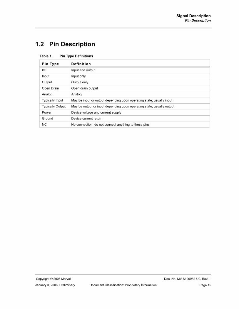
1.2 Pin Description
Table 1: Pin Type Definitions
Pin Type Definit ion
I/O Input and output
Input Input only
Output Output only
Open Drain Open drain output
Analog Analog
Typically Input May be input or output depending upon operating state; usually input
Typically Output May be output or input depending upon operating state; usually output
Power Device voltage and current supply
Ground Device current return
NC No connection, do not connect anything to these pins

Link Street® 88E6060 - UnrestrictedLow Power, 6-port, 10/100 Ethernet Switch
Doc. No. MV-S100952-U0, Rev. -- Copyright © 2008 Marvell
Page 16 Document Classification: Proprietary Information January 3, 2008, Preliminary
Table 2: Network Interface
128-PQFP PackagePin #
Pin Name Pin Type Description
272515134
P[4:0]_RXP Typically InputOutput if in Crossover mode
Receiver input – Positive. P[4:0]_RXP connects directly to the receiver magnetics. If the port is configured for 100BASE-FX mode (ports 0 and 1 only) RXP connects directly to the fiber-optic receiver’s positive output. These pins can become out-puts if Auto MDI/MDIX Crossover is enabled (see section 4.6).
If a PHY port is not used, the RXP pins should be tied to VSS.
282416125
P[4:0]_RXN Typically Input Output if in Crossover mode
Receiver input – Negative. P[4:0]_RXN connects directly to the receiver magnetics. If the port is configured for 100BASE-FX mode (ports 0 and 1 only) RXN connects directly to the fiber-optic receiver’s negative output. These pins can become outputs if Auto MDI/MDIX Crossover is enabled (see section 4.6).
If a PHY port is not used, the RXN pins should be tied to VSS.
302218107
P[4:0]_TXP Typically Output Input if in Crossover mode
Transmitter output – Positive. P[4:0]_TXP connects directly to the transmitter magnetics. If the port is configured for 100BASE-FX mode (ports 0 and 1 only) TXP connects directly to the fiber-optic transmitter’s positive input. These pins can become inputs if Auto MDI/MDIX Crossover is enabled (see section 4.6).
If a PHY port is not used, the TXP pins should be tied to VSS.
31211998
P[4:0]_TXN Typically Output Input if in Crossover mode
Transmitter output – Negative. P[4:0]_TXN connects directly to the transmitter magnetics. If the port is configured for 100BASE-FX mode (ports 0 and 1 only) TXN connects directly to the fiber-optic transmitter’s negative input. These pins can become inputs if Auto MDI/MDIX Crossover is enabled (see section 4.6).
If a PHY port is not used, the TXN pins should be tied to VSS.
127122
P[1:0]_SDET Input Signal Detect input. If port 0 and/or 1 is configured for 100BASE-FX mode SDET indicates whether a signal is detected by the fiber-optic transceiver. A positive level indi-cates that a signal is detected.
If port 0 and/or 1 is configured for 10/100BASE-T mode SDET is not used, but cannot be left floating since these pins do not contain internal resistors. SDET must be tied to VSS or VDDO either directly or through a 4.7 kΩ resistor.

Signal DescriptionPin Description
Copyright © 2008 Marvell Doc. No. MV-S100952-U0, Rev. --
January 3, 2008, Preliminary Document Classification: Proprietary Information Page 17
Table 3: PHY Configuration
128-PQFPPackagePin #
Pin Name PinType
Description
108111
P[1:0]_CONFIG Input Port 0 and 1 Configuration. The CONFIG pin is used to set the default configuration for Port 0 and 1 by connecting these pins to other device pins as follows:
VSS = Auto-Negotiation enabled - default P0_LED1 = Forced 10BASE-T half-duplex P0_LED2 = Forced 10BASE-T full-duplex P1_LED0 = Forced 100BASE-TX half-duplex P1_LED1 = Forced 100BASE-TX full-duplex P1_LED2 = Forced 100BASE-FX half-duplex VDDO = Forced 100BASE-FX full-duplex
Ports 2, 3 and 4’s default configuration is Auto-Negotiation enabled. Any port’s default configuration can be modified by accessing the PHY registers by a CPU or a serial EEPROM. Fiber vs. copper mode cannot be configured in this way. How-ever, Fiber vs. copper must be selected at reset by using these pins.
The CONFIG pins are configured after reset and contain inter-nal pull-down resistors so they can be left floating to select Auto-Negotiation.
106 CONFIG_A Input Global Configuration A. This global configuration pin is used to set the default LED mode and Far End Fault Indication (FEFI) mode for 100BASE-FX by connecting these pins to other device pins as follows:
VSS = LED Mode 0, FEFI disabled P0_LED0 = LED Mode 0, FEFI enabled P0_LED1 = LED Mode 1, FEFI disabled P0_LED2 = LED Mode 1, FEFI enabled P1_LED0 = LED Mode 2, FEFI disabled P1_LED1 = LED Mode 2, FEFI enabled P1_LED2 = LED Mode 3, FEFI disabled VDDO = LED Mode 3, FEFI enabled - default
The LED modes are covered in section 4.7.1 and FEFI is cov-ered in section 4.2.8.3.
The CONFIG_A pin is configured after reset and contains an internal pull-up resistor.

Link Street® 88E6060 - UnrestrictedLow Power, 6-port, 10/100 Ethernet Switch
Doc. No. MV-S100952-U0, Rev. -- Copyright © 2008 Marvell
Page 18 Document Classification: Proprietary Information January 3, 2008, Preliminary
93 CONFIG_B Input Global Configuration B. This global configuration pin is used to set the default mode for Auto Crossover, the PHY driver type, and Energy Detect by connecting these pins to other device pins as follows:
VSS = No Crossover, Class A1 drivers, Energy Detect dis-abled
P0_LED0 = No Crossover, Class A drivers, Energy Detect enabled
P0_LED1 = No Crossover, Class B2 drivers, EnergyDetect disabled
P0_LED2 = No Crossover, Class B drivers, Energy Detect enabled
P1_LED0 = Auto Crossover, Class A drivers, Energy Detect disabled
P1_LED1 = Auto Crossover, Class A drivers, Energy Detect enabled
P1_LED2 = Auto Crossover, Class B drivers, Energy Detect disabled
VDDO = Auto Crossover, Class B drivers, Energy Detect enabled—default
Auto crossover is covered in section 4.6, Class B vs. Class A drivers are covered in Table 83 on page 132 and Energy Detect is covered in section Table 71 through Table 74.
The CONFIG_B pin is configured after reset and contains an internal pull-up resistor.
1. A Class A driver is available for 100BASE-TX mode only and typically used in backplane or direct connect applications.2. A Class B driver is typically used in CAT 5 applications.
Table 3: PHY Configuration (Continued)
128-PQFPPackagePin #
Pin Name PinType
Description

Signal DescriptionPin Description
Copyright © 2008 Marvell Doc. No. MV-S100952-U0, Rev. --
January 3, 2008, Preliminary Document Classification: Proprietary Information Page 19
Table 4: Regulator and Reference
128-PQFPPackagePin #
Pin Name PinType
Description
126 RSETP Analog Resistor reference. A 2 kΩ 1% resistor is placed between the RSETP and RSETN. This resistor is used to set an internal bias reference current.
125 RSETN Analog Resistor reference. A 2 kΩ 1% resistor is placed between the RSETN and RSETP. This resistor is used to set an internal bias reference current.
124 CONTROL_15 Analog Voltage control to external 1.5V regulator. This signal con-trols an external PNP transistor to generate the 1.5V power supply for the VDD and VDDAL pins.
2 CONTROL_25 Analog Voltage control to external 2.5V regulator. This signal con-trols an external PNP transistor to generate the 2.5V power supply for the VDDAH pins.
Table 5: System
128-PQFP PackagePin #
Pin Name Pin Type Description
104 XTAL_IN Input 25 MHz or 50 MHz system reference clock input. The fre-quency of this clock input is selected by the CLK_SEL pin. The clock source can come from a crystal (25 MHz only) or an oscillator (25 or 50 MHz). This is the only clock required as it is used for both the switch and the PHYs.
105 XTAL_OUT Output System reference clock output. This output can only be used to drive an external crystal (25 MHz only). It cannot be used to drive external logic. If an oscillator is connected to XTAL_IN this pin should be left unconnected.
68 CLK_SEL Input Clock frequency Select. Connect this pin to VSS if XTAL_IN is 25 MHz. Connect this pin to VDDO or leave it unconnected if XTAL_IN is 50 MHz. This pin must be stable before and after reset.
CLK_SEL is internally pulled high via a resistor.
110 RESETn Input Hardware reset. Active low. The 88E6060 is configured dur-ing reset. When RESETn is low all configuration pins become inputs and the value seen on these pins is latched on the ris-ing edge of RESETn or some time after.

Link Street® 88E6060 - UnrestrictedLow Power, 6-port, 10/100 Ethernet Switch
Doc. No. MV-S100952-U0, Rev. -- Copyright © 2008 Marvell
Page 20 Document Classification: Proprietary Information January 3, 2008, Preliminary
Table 6: Register Access Interface
128-PQFPPackagePin #
Pin Name Pin Type Description
70 MDC Input MDC is the management data clock reference for the serial management interface (SMI). A continuous clock stream is not expected. The maximum frequency supported is 8.3 MHz.
The SMI is used to access the registers in the PHY and in the Switch if the serial EEPROM is not accessing the registers. It is available in all combinations of SW_MODE[1:0].
MDC is internally pulled high via a resistor.
71 MDIO I/O MDIO is the management data Input/Output for the SMI. MDIO is used to transfer management data in and out of the device synchronously with MDC. This pin requires an external pull-up resistor in the range of 4.7 kΩ to 10 kΩ.
The 88E6060 device uses 16 of the 32 possible SMI port addresses. The 16 that are used are selectable using the EE_CLK/ADDR4 pin.
MDIO is internally pulled high via a resistor.
63 INTn Open Drain Output
INTn is an active low, open drain pin that is asserted to indi-cate an unmasked interrupt event occurred. A single external pull-up resistor is required to achieve a logic high when this signal is inactive.
The INTn pin is asserted active low if SW_MODE[1:0] (see Table 14) bits are not 0b10 (standalone mode) and the EEPROM data has been completely read into the device. This EEPROM done interrupt indicates to any attached CPU that it may use the MDC/MDIO lines to access the internal registers because the EEPROM has finished using the registers. This pin also goes low when any other unmasked interrupt becomes active inside the device.

Signal DescriptionPin Description
Copyright © 2008 Marvell Doc. No. MV-S100952-U0, Rev. --
January 3, 2008, Preliminary Document Classification: Proprietary Information Page 21
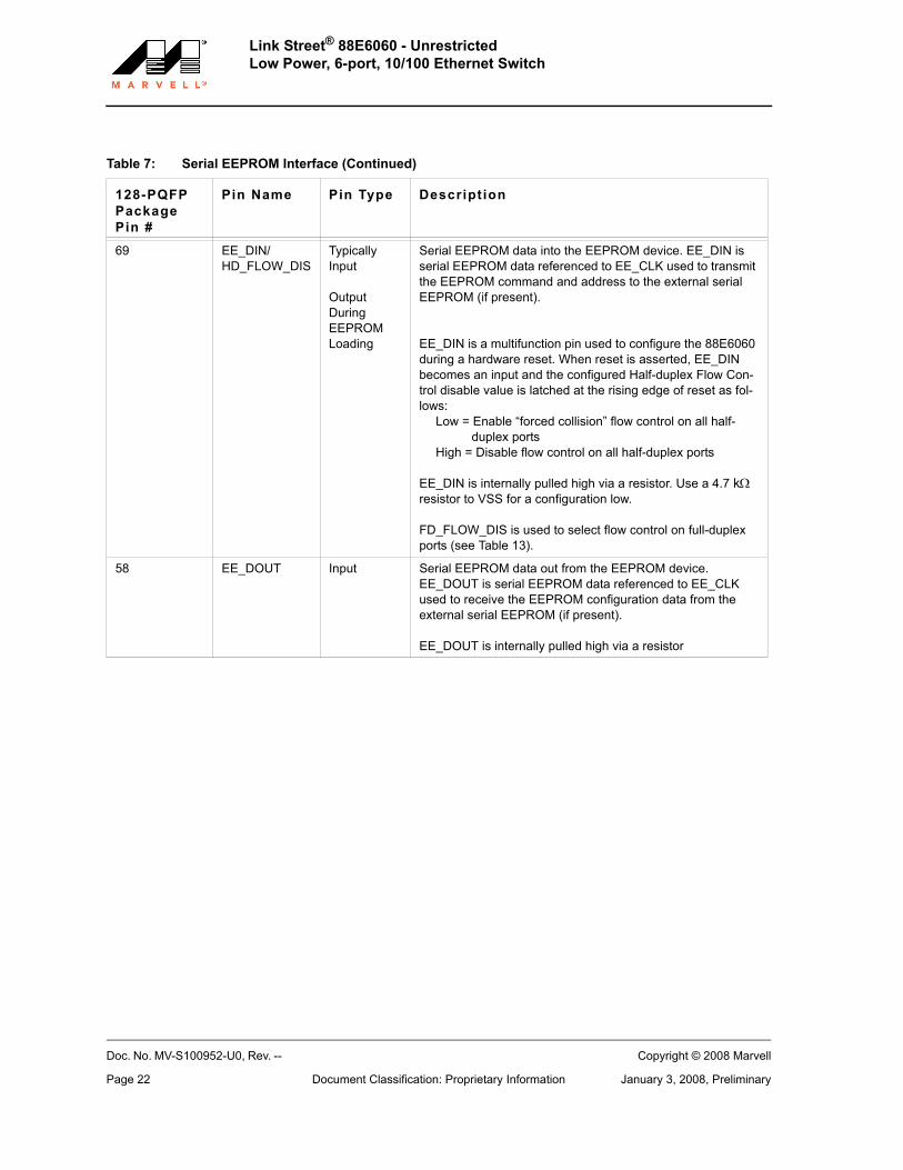
Table 7: Serial EEPROM Interface
128-PQFPPackagePin #
Pin Name Pin Type Description
61 EE_CS/EE_1K
I/O
Input during reset
Serial EEPROM chip select. EE_CS is the serial EEPROM chip select referenced to EE_CLK. It is used to enable the external EEPROM (if present), and to delineate each data transfer.
EE_CS is a multi-function pin used to configure the 88E6060 during a hardware reset. When reset is asserted, EE_CS becomes an input and the desired EEPROM type configura-tion is latched at the rising edge of RESETn as follows: Low = Use 8-bit addresses (for 2K bit 93C56 & 4K bit
93C66) High = Use 6-bit addresses (for 1K bit 93C46)
The external EEPROM must be configured in the x16 organi-zation.
EE_CS is internally pulled high via a resistor. Use a 4.7 kΩ resistor to VSS for a configuration low.
60 EE_CLK/ADDR4
I/O
Output During EEPROMLoading
Serial EEPROM clock. EE_CLK is the serial EEPROM clock reference output by the 88E6060. It is used to shift the exter-nal serial EEPROM (if installed) to the next data bit so the default values of the internal registers can be overridden.
EE_CLK is a multi-function pin used to configure the 88E6060 during a hardware reset. When reset is asserted, EE_CLK becomes an input and the desired SMI ADDR4 address space configuration (Table 5) is latched at the rising edge of RESETn as follows: Low = Use SMI device addresses 0x00 to 0x0F High = Use SMI device addresses 0x10 to 0x1F
EE_CLK is internally pulled high via a resistor. Use a 4.7 kΩ resistor to VSS for a configuration low.
Link Street® 88E6060 - UnrestrictedLow Power, 6-port, 10/100 Ethernet Switch
Doc. No. MV-S100952-U0, Rev. -- Copyright © 2008 Marvell
Page 22 Document Classification: Proprietary Information January 3, 2008, Preliminary
69 EE_DIN/HD_FLOW_DIS
TypicallyInput
Output During EEPROMLoading
Serial EEPROM data into the EEPROM device. EE_DIN is serial EEPROM data referenced to EE_CLK used to transmit the EEPROM command and address to the external serial EEPROM (if present).
EE_DIN is a multifunction pin used to configure the 88E6060 during a hardware reset. When reset is asserted, EE_DIN becomes an input and the configured Half-duplex Flow Con-trol disable value is latched at the rising edge of reset as fol-lows:
Low = Enable “forced collision” flow control on all half-duplex ports
High = Disable flow control on all half-duplex ports
EE_DIN is internally pulled high via a resistor. Use a 4.7 kΩ resistor to VSS for a configuration low.
FD_FLOW_DIS is used to select flow control on full-duplex ports (see Table 13).
58 EE_DOUT Input Serial EEPROM data out from the EEPROM device. EE_DOUT is serial EEPROM data referenced to EE_CLK used to receive the EEPROM configuration data from the external serial EEPROM (if present).
EE_DOUT is internally pulled high via a resistor
Table 7: Serial EEPROM Interface (Continued)
128-PQFPPackagePin #
Pin Name Pin Type Description

Signal DescriptionPin Description
Copyright © 2008 Marvell Doc. No. MV-S100952-U0, Rev. --
January 3, 2008, Preliminary Document Classification: Proprietary Information Page 23
Table 8: Port 5’s Enable
128-PQFPPackagePin #
Pin Name Pin Type Description
66 ENABLE_MII5 Input Enable MII Port 5. This pin is used to enable Port 5. A high enables the Port. A low disables Port 5 (i.e., the drivers are tri-stated).
ENABLE_P5 is internally pulled high via a resistor.
Table 9: Port 5’s Input MII—If ENABLE_MII5 = High
128-PQFPPackagePin #
Pin Name Pin Type Description
82 P5_INCLK I/O Input Clock. P5_INCLK is a reference for P5_INDV and P5_IND[3:0]. The direction and speed of P5_INCLK is deter-mined by P5_MODE[3:0] at the end of reset.
If the port is in PHY Mode, P5_INCLK is an output. In this mode the frequency of the clock is 25 MHz if the port is in 100BASE-X mode, 2.5 MHz if the port is in 10BASE-T mode and 50 MHz for RMII mode.
If the port is in MAC Mode, P5_INCLK is an input. In this mode the frequency of the clock can be anywhere from DC to 25 MHz although it should be 25 MHz for 100BASE-X mode and 2.5 MHz for 10BASE-T mode.
P5_INCLK is tri-stated during reset and it is internally pulled high.
83848586
P5_IND[3:0] Input Input Data. P5_IND[3:0] receives the data nibble to be trans-mitted into the switch in 100BASE-X and 10BASE-T modes. P5_IND[3:0] is synchronous to P5_INCLK. These pins are inputs regardless of the port’s mode (i.e., PHY mode or MAC mode). Only P5_IND0 is used when SNI mode is selected. P5_IND[1:0] are used when RMII mode is selected1.
P5_IND[3:0] are internally pulled high via resistor.
1. When RMII mode is selected P5_IND[1:0] are synchronous to P5_OUTCLK or P5_INCLK which are phase shifted to each other.
87 P5_INDV Input Input Data Valid. When P5_INDV is asserted high, data on P5_IND[3:0] is accepted into the switch. P5_INDV must be synchronous to P5_INCLK for SNI and MII operation. It must be synchronous to P5_OUTCLK or P5_INCLK in RMII opera-tion.
P5_INDV is internally pulled low via resistor.

Link Street® 88E6060 - UnrestrictedLow Power, 6-port, 10/100 Ethernet Switch
Doc. No. MV-S100952-U0, Rev. -- Copyright © 2008 Marvell
Page 24 Document Classification: Proprietary Information January 3, 2008, Preliminary
Table 10: Port 5’s Output MII—If ENABLE_MII5 = High
128-PQFPPackagePin #
Pin Type Pin Name Description
79 P5_OUTCLK I/O Output Clock. P5_OUTCLK is a reference for P5_OUTDV and P5_OUTD[3:0]. The direction and speed of P5_OUTCLK is determined by P5_MODE[3:0] at the end of reset.
If the port is in PHY Mode, P5_OUTCLK is an output. In this mode the frequency of the clock will be 25 MHz if the port is in 100BASE-X mode, and 2.5 MHz if the port is in 10BASE-T mode and 50 MHz for RMII mode.
If the port is in MAC Mode, P5_OUTCLK is an input. In this mode the frequency of the clock can be anywhere from DC to 25MHz although it should be 25 MHz for 100BASE-X mode and 2.5 MHz for 10BASE-T mode.
P5_OUTCLK is tri-stated during reset and it is internally pulled high.
74757677
P5_OUTD[3:0]/P5_MODE[3:0]
Normally Output
Input only when RESETn is low
Output Data. Data transmitted from the switch is decoded and presented on P5_OUTD[3:0] pins synchronous to P5_OUT_CLK. These pins are outputs regardless of the port’s mode (i.e., PHY or MAC mode). Only P5_OUTD0 con-tains meaningful data when SNI mode is selected. P5_OUTD[1:0] are used when RMII mode1 is selected.
During reset, these internally pulled high pins are tri-stated and used to latch in the required operating mode for the port (see section.3.2.5).
1. P5_OUTD[1:0] can be synchronous to either P5_OUTCLK or P5_INCLK, which are phase shifted to each other.
81 P5_OUTDV Output Output Data Valid. When P5_OUTDV is asserted high, data transmitted from the switch on P5_OUTD[3:0] is valid. P5_OUTDV is synchronous with P5_OUTCLK in MII mode. When RMII mode is selected, P5_OUTDV can be synchro-nous to either P5_INCLK or P5_OUTCLK.
P5_OUTDV is tri-stated during reset and it is internally pulled high.
72 P5_CRS I/O
Carrier Sense. After reset, P5_CRS becomes an output if PHY Mode is selected for this port. It remains an input if MAC Mode is selected. P5_CRS asserts (or is expected to be asserted) when the receive data path is non-idle. In half-duplex mode P5_CRS is also asserted (or is expected to be asserted) during transmission. P5_CRS is asynchronous to P5_OUTCLK and P5_INCLK.
P5_CRS is tri-stated during reset and it is internally pulled low so the pin can be left unconnected if not used.

Signal DescriptionPin Description
Copyright © 2008 Marvell Doc. No. MV-S100952-U0, Rev. --
January 3, 2008, Preliminary Document Classification: Proprietary Information Page 25
Table 10: Port 5’s Output MII—If ENABLE_MII5 = High (Continued)
128-PQFPPackagePin #
Pin Type Pin Name Description
73 P5_COL I/O
Collision. After reset, P5_COL becomes an output if PHY Mode is selected for this port. It remains an input if MAC Mode is selected. In PHY Mode, P5_COL asserts when both the transmit and receive paths are non-idle in both half and full-duplex modes. In half-duplex, MAC mode P5_COL is expected to be asserted when both the transmit and receive paths are non-idle. In full-duplex MAC mode, P5_COL is ignored. P5_COL is asynchronous with P5_OUTCLK and P5_INCLK.
P5_COL is tri-stated during reset and it is internally pulled low.

Link Street® 88E6060 - UnrestrictedLow Power, 6-port, 10/100 Ethernet Switch
Doc. No. MV-S100952-U0, Rev. -- Copyright © 2008 Marvell
Page 26 Document Classification: Proprietary Information January 3, 2008, Preliminary
Table 11: Port 4’s Enable
128-PQFPPackagePin #
Pin Name Pin Type Description
89 DISABLE_MII4 Input Disable MII Port 4. This pin is used to disable Port 4’s MII Interface drivers. A high disables Port 4’s MII interface driv-ers’s MII interface (i.e., the drivers are tri-stated) and enables Port 4’s PHY interface (its MDI pins). A low enables Port 4’s MII Interface and its drivers and disables Port 4’s PHY inter-face.
DISABLE_MII4 is internally pulled high via a resistor.
Table 12: Port 4’s Input MII—If DISABLE_MII4 = Low
128-PQFPPackagePin #
Pin Name Pin Type Description
102 P4_INCLK I/O Input Clock. P4_INCLK is a reference for P4_INDV and P4_IND[3:0]. The direction and speed of P4_INCLK is deter-mined by P4_MODE[3:0] at the end of reset.
If the port is in PHY Mode, P4_INCLK is an output. In this mode the frequency of the clock will be 25 MHz if the port is in 100BASE-X mode, and 2.5 MHz if the port is in 10BASE-T mode and 50 MHz for RMII mode.
If the port is in MAC Mode, P4_INCLK is an input. In this mode the frequency of the clock can be anywhere from DC to 25 MHz although it should be 25 MHz for 100BASE-X mode and 2.5 MHz for 10BASE-T mode.
P4_INCLK is tri-stated during reset and it is internally pulled high.
112114116117
P4_IND[3:0] Input Input Data. P4_IND[3:0] receives a data nibble to be transmitted into the switch in 100BASE-X and 10BASE-T modes. P4_IND[3:0] is synchronous with P4_INCLK. These pins are inputs regardless of the port’s mode (i.e., PHY or MAC mode). Only P4_IND0 is used when SNI mode is selected. P4_IND[1:0] are used when RMII mode is selected1.
P4_IND[3:0] are internally pulled high via resistor.
1. When RMII mode is selected, P4_IND[1:0] are synchronous to P4_OUTCLK or P4_INCLK, which are phase shifted to each other.
118 P4_INDV Input Input Data Valid. When P4_INDV is asserted high, data on P4_IND[3:0] is accepted into the switch. P4_INDV must be syn-chronous to P4_INCLK for SNI and MII operation. It must be synchronous to P4_OUTCLK or P4_INCLK in RMII operation.
P4_INDV is internally pulled low via resistor.

Signal DescriptionPin Description
Copyright © 2008 Marvell Doc. No. MV-S100952-U0, Rev. --
January 3, 2008, Preliminary Document Classification: Proprietary Information Page 27
Table 13: Port 4’s Output MII—If DISABLE_MII4 = Low
128-PQFPPackagePin #
Pin Name Pin Type Description
99 P4_OUTCLK I/O Output Clock. P4_OUTCLK is a reference for P4_OUTDV and P4_OUTD[3:0]. The direction and speed of P4_OUTCLK is determined by P4_MODE[3:0] at the end of reset.
If the port is in PHY Mode, P4_OUTCLK is an output. In this mode the frequency of the clock will be 25 MHz if the port is in 100BASE-X mode, and 2.5 MHz if the port is in 10BASE-T mode and 50 MHz for RMII mode.
If the port is in MAC Mode, P4_OUTCLK is an input. In this mode the frequency of the clock can be anywhere from DC to 25MHz although it should be 25 MHz for 100BASE-X mode and 2.5 MHz for 10BASE-T mode.
P4_OUTCLK is tri-stated during reset and it is internally pulled high.
95969798
P4_OUTD[3:0]/P4_MODE[3:0]
Normally Output
Input only when RESETn is low
Output Data. Data transmitted from the switch is decoded and presented on P4_OUTD[3:0] pins synchronous to P4_OUT_CLK. These pins are outputs regardless of the port’s mode (i.e., PHY or MAC mode). Only P4_OUTD0 con-tains data when SNI mode is selected. P4_OUTD[1:0] are used when RMII mode1 is selected.
During reset these internally pulled high pins are tri-stated and used to latch in the desired operating mode for the port (see section 3.2.5).
1. P4_OUTD[1:0] can be synchronous to either P4_OUTCLK or P4_INCLK, which are phase shifted to each other.
100 P4_OUTDV Output Output Data Valid. When P4_OUTDV is asserted high, data transmitted from the switch on P4_OUTD[3:0] is valid. P4_OUTDV is synchronous with P4_OUTCLK in MII Mode.When RMII mode is selected, P4_OUTDV can be synchro-nous to either P5_INCLK or P4_OUTCLK.
P4_OUTDV is tri-stated during reset and it is internally pulled high.
91 P4_CRS I/O
Carrier Sense. After reset, P4_CRS becomes an output if PHY Mode is selected for this port. It remains an input if MAC Mode is selected. P4_CRS asserts (or is expected to be asserted) when the receive data path is non-idle. In half-duplex mode P4_CRS is also asserted (or is expected to be asserted) during transmission. P4_CRS is asynchronous to P4_OUTCLK and P4_INCLK.
P4_CRS is tri-stated during reset and it is internally pulled low.

Link Street® 88E6060 - UnrestrictedLow Power, 6-port, 10/100 Ethernet Switch
Doc. No. MV-S100952-U0, Rev. -- Copyright © 2008 Marvell
Page 28 Document Classification: Proprietary Information January 3, 2008, Preliminary
Table 13: Port 4’s Output MII—If DISABLE_MII4 = Low (Continued)
128-PQFPPackagePin #
Pin Name Pin Type Description
94 P4_COL I/O
Collision. After reset, P4_COL becomes an output if PHY Mode is selected for this port. It remains an input if MAC Mode is selected. In PHY Mode, P4_COL asserts when both the transmit and receive paths are non-idle in both half and full-duplex modes. In half-duplex, MAC mode P4_COL is expected to be asserted when both the transmit and receive paths are non-idle. In full-duplex MAC mode, P4_COL is ignored. P4_COL is asynchronous to P4_OUTCLK and P4_INCLK.
P4_COL is tri-stated during reset and it is internally pulled low.

Signal DescriptionPin Description
Copyright © 2008 Marvell Doc. No. MV-S100952-U0, Rev. --
January 3, 2008, Preliminary Document Classification: Proprietary Information Page 29
Table 14: Switch Configuration Interface
128-PQFPPackagePin #
Pin Name Pin Type Description
3433
SW_MODE[1:0] Input Switch Mode. These pins are used to configure the 88E6060 after reset. Switch Mode pins work as follows:
1 0 Description 0 0 CPU attached mode – ports come up disabled1
0 1 Reserved 1 0 Stand alone mode - ignore EEPROM 1 1 EEPROM attached mode2
The EEPROM attached mode (when both SW_MODE pins = high) can be used with a CPU. In all but the standalone modes, the INTn pin asserts active low after the EEPROM completes initializing the internal registers (i.e. a halt com-mand has been executed)3.
SW_MODE[1:0] are not latched on the rising edge of Reset and they must remain static for proper device operation. They are internally pulled high via resistors.
1. The ports come up in the Disabled Port State in the CPU mode so the CPU can perform bridge loop detection on link up and/or per-form switch initialization/configuration prior to letting packets flow.
2. In EEPROM attached mode the ports come up in the Forwarding Port State unless the Port Control register is overwritten by the EEPROM data.
3. The INTn pin is activated so the CPU can access the registers using the MDC/MDIO pins. The CPU cannot access these registers as long as the EEPROM is still being executed.
64 FD_FLOW_DIS Input Full-duplex Flow Control disable. High = disable flow control on all full-duplex ports Low = enable IEEE 802.3x Pause based flow control on all supported full-duplex ports
Full-duplex flow control requires support from the end station. Full-duplex flow control is supported on any full-duplex port that has Auto-Negotiation enabled, advertises that it supports Pause (i.e., FD_FLOW_DIS = Low at reset), and sees that the end station supports Pause as well (from data returned during Auto-Negotiation). If any of these requirements are not met the port does not generate Pause frames and it does not pause when the port receives Pause frames.
FD_FLOW_DIS is latched on the rising edge of Reset into all the port’s PHY Auto-Negotiation Advertisement registers. It is internally pulled high via a resistor.
The EE_DIN/HD_FLOW_DIS multi-function pin is used to select Flow control on half-duplex ports (see Table 7)

Link Street® 88E6060 - UnrestrictedLow Power, 6-port, 10/100 Ethernet Switch
Doc. No. MV-S100952-U0, Rev. -- Copyright © 2008 Marvell
Page 30 Document Classification: Proprietary Information January 3, 2008, Preliminary
Table 15: Port Status LEDs
128-PQFPPackagePin #
Pin Name Pin Type Description
3943465054
P[4:0]_LED2 Output Parallel LED outputs – one for each port. This active low LED pin directly drives an LED in Parallel LED mode. It can be con-figured to display many options.
P[4:0]_LED2 are driven active low whenever RESETn is asserted.
4044485155
P[4:0]_LED1 Output Parallel LED outputs – one for each port. This active low LED pin directly drives an LED in Parallel LED mode. It can be con-figured to display many options.
P[4:0]_LED1 are driven active low whenever RESETn is asserted.
4145495356
P[4:0]_LED0 Output Parallel LED outputs – one for each port. This active low LED pin directly drives an LED in Parallel LED mode. It can be con-figured to display many options.
P[4:0]_LED0 are driven active low whenever RESETn is asserted.
36 LEDSER Output LEDSER outputs serial status bits that can be shifted into a shift register to be displayed via LEDs. LEDSER is output synchro-nously to LEDCLK.
38 LEDENA Output LEDENA asserts High whenever LEDSER has valid status that is to be stored into the shift register. LEDENA is output synchro-nously to LEDCLK.
37 LEDCLK Output LEDCLK is the reference clock for the serial LED signals.

Signal DescriptionPin Description
Copyright © 2008 Marvell Doc. No. MV-S100952-U0, Rev. --
January 3, 2008, Preliminary Document Classification: Proprietary Information Page 31
Table 16: Power and Ground
128-PQFPPackagePin #
Pin Name Pin Type Description
4778107123
VDDO Power Power to P4 and P5 MIIs, LED, EEPROM, and I/O drivers. VDDO must be connected to 3.3V.
31426
VDDAH Power 2.5 volt analog power to PHYs
611172329
VDDAL Power 1.5 volt power to analog core
35576590101113
VDD Power 1.5 volt power to digital core
12032425259678092103109115128
VSS Ground Ground to device
6288119120121
NC - No Connect. These pins must be left unconnected.

Doc. No. MV-S100952-U0 Rev. -- Copyright © 2008 Marvell
Page 32 Document Classification: Proprietary Information January 3, 2008, Preliminary
Link Street® 88E6060 - UnrestrictedLow Power, 6-port, 10/100 Ethernet Switch
1.3 128-Pin LQFP Pin Assignment List—by Signal Name
Table 17: Package Pin List—Alphabetical by Signal Name
Pin Number
Pin Name
68 CLK_SEL
106 CONFIG_A
93 CONFIG_B
124 CONTROL_15
2 CONTROL_25
89 DISABLE_MII4
60 EE_CLK/ADDR4
61 EE_CS/EE_1K
69 EE_DIN/HD_FLOW_DIS
58 EE_DOUT
66 ENABLE_MII5
64 FD_FLOW_DIS
63 INTn
37 LEDCLK
38 LEDENA
36 LEDSER
70 MDC
71 MDIO
62 NC
88 NC
119 NC
120 NC
121 NC
111 P0_CONFIG
56 P0_LED0
55 P0_LED1
54 P0_ LED2
5 P0_RXN
4 P0_RXP
122 P0_SDET
8 P0_TXN
7 P0_TXP
108 P1_CONFIG
53 P1_LED0
51 P1_LED1
50 P1_LED2
12 P1_RXN
13 P1_RXP
127 P1_SDET
9 P1_TXN
10 P1_TXP
49 P2_LED0
48 P2_LED1
46 P2_LED2
16 P2_RXN
15 P2_RXP
19 P2_TXN
18 P2_TXP
45 P3_LED0
44 P3_LED1
43 P3_LED2
24 P3_RXN
25 P3_RXP
21 P3_TXN
22 P3_TXP
41 P4_LED0
40 P4_LED1
39 P4_LED2
28 P4_RXN
27 P4_RXP
31 P4_TXN
30 P4_TXP
73 P5_COL
72 P5_CRS
Pin Number
Pin Name

Copyright © 2008 Marvell Doc. No. MV-S100952-U0 Rev. --
January 3, 2008, Preliminary Document Classification: Proprietary Information Page 33
Signal Description128-Pin LQFP Pin Assignment List—by Signal Name
82 P5_INCLK
86 P5_IND0
85 P5_IND1
84 P5_IND2
83 P5_IND3
87 P5_INDV
79 P5_OUTCLK
77 P5_OUTD0/P5_MODE0
76 P5_OUTD1/P5_MODE1
75 P5_OUTD2/P5_MODE2
74 P5_OUTD3/P5_MODE3
81 P5_OUTDV
94 P4_COL
91 P4_CRS
102 P4_INCLK
117 P4_IND0
116 P4_IND1
114 P4_IND2
112 P4_IND3
118 P4_INDV
99 P4_OUTCLK
98 P4_OUTD0/P4_MODE0
97 P4_OUTD1/P4_MODE1
96 P4_OUTD2/P4_MODE2
95 P4_OUTD3/P4_MODE3
100 P4_OUTDV
110 RESETn
125 RSETN
126 RSETP
33 SW_MODE0
34 SW_MODE1
35 VDD
57 VDD
65 VDD
90 VDD
Pin Number
Pin Name
101 VDD
113 VDD
3 VDDAH
14 VDDAH
26 VDDAH
6 VDDAL
11 VDDAL
17 VDDAL
23 VDDAL
29 VDDAL
47 VDDO
78 VDDO
107 VDDO
123 VDDO
1 VSS
20 VSS
32 VSS
42 VSS
52 VSS
59 VSS
67 VSS
80 VSS
92 VSS
103 VSS
115 VSS
109 VSS
128 VSS
104 XTAL_IN
105 XTAL_OUT
Pin Number
Pin Name

Link Street® 88E6060 - UnrestrictedLow Power, 6-port, 10/100 Ethernet Switch
Doc. No. MV-S100952-U0, Rev. -- Copyright © 2008 Marvell
Page 34 Document Classification: Proprietary Information January 3, 2008, Preliminary
Section 2. Application Examples
The Marvell® 88E6060 device supports many different applications with few additional active components in a small footprint. The 88E6060 contains six ports with five PHYs. This architecture allows all five PHYs to be active and available while at the same time supporting one independent MII interface.
The higher integration, low power, and an extra port saves BOM costs on designs requiring six ports or two MII interfaces. The flexibility of the 88E6060 device comes from its configuration options on Port 0 and Port 1, and its configuration options on its two MII ports (Port 5’s MII interface is always on, while Port 4 can be an MII or a PHY). The device also supports an optional EEPROM (93C46 type) to override any of the default settings.
The only active components required to implement a complete 88E6060 10/100 Ethernet switch are:
• 25 MHz crystal clock source or a 25 or 50 MHz oscillator • Low-cost PNP transistor used to regulate 2.5V down from 3.3V• Low-cost PNP transistor used to regulate 1.5V down from 3.3V
The 88E6060 is a full system on a chip containing the PHYs, LED drivers, voltage regulator logic, switch logic, and memory. In addition, it is pin compatible with the Marvell® 88E6063 QoS switch.
2.1 Examples with the 88E6060The 88E6060 has multiple configuration options selectable through four pins: P[1:0]_CONFIG, ENABLE_MII5, and DISABLE_MII4. Table 1 shows Port 0 and Port 1 Copper or Fiber configuration settings, and Port 5 and Port 4 configuration settings. Ports 2, 3, and 4’s default configuration is Auto-Negotiation enabled.
Table 18: 88E6060 Port Configuration
P0_CONFIG P1_CONFIG ENABLE_MII5 DISABLE_MII4 Port Mode
Low X X X Port 0 = Copper Auto-Negotiation
High X X X Port 0 = Fiber Mode
X Low X X Port 1 = Copper Auto-Negotiation
X High X X Port 1 = Fiber Mode
X X Low X Port 5 = Disabled
X X High X Port 5 = RMII/MII/SNI Mode
X X X Low Port 4 = RMII/MII/SNI Mode
X X X High Port 4 = Copper Auto-Negotiation

Application ExamplesExamples with the 88E6060
Copyright © 2008 Marvell Doc. No. MV-S100952-U0, Rev. --
January 3, 2008, Preliminary Document Classification: Proprietary Information Page 35
Each of the following modes are described in detail below:
• Firewall Router Switch w/four 10/100BASE-T LAN ports & one 10/100BASE-T WAN port • Firewall Router Switch supporting a Fiber WAN port (using port 0 or port 1)• Firewall Router Switch with four 10/100BASE-T LAN ports & an MII port for a WAN PHY (using port 4)
For the firewall router examples, Port 5 is configured in PHY Mode, and Ports 0 to 4 support 100BASE-TX and/or 10BASE-T operation. Port 0 could be 100BASE-FX if desired as a fiber interface from the WAN (see Figure 3). The CPU’s SMI is used to access all the PHY and Switch registers inside the 88E6060.
In Figure 2, Port 0 is used as a WAN interface in the LAN. To make this work, the WAN port needs to be isolated from the LAN ports, and vice versa. LAN frames cannot go directly to the WAN, and WAN frames cannot go directly to the LAN. The CPU’s port needs to be the bridge by transmitting, receiving, and translating frames from both the WAN and to and from the LAN. The 88E6060 supports port based VLANs in any programmable configu-ration that support this requirement and a Marvell header mode supports dynamic VLANs on the CPU’s port.
Bringing the 802.3 WAN PHY into the 88E6060’s Port 0 not only reduces BOM costs, but it also adds the feature of a 10/100 Mbps interface with Auto Crossover cable support (supported on all copper ports).
Figure 2: 88E6060 Firewall Router ExamplePo
rt 5
5x TX or4x TX + 1 FX
Port 1 Port 2 Port 3 Port 4
88E6060 Parallel LEDLines
NC
Port 0
WAN LAN
ENABLE_MII5
TX_E
RTX
_EN
TXD
[3:0
]TX
_CLK
RX_
DV
RX_
CLK
RXD
[3:0
]C
OL
CR
S
Router Chipwith MAC
MD
IOM
DC
SMI
25 MHz XTAL®
®2.5V
CONTROL_15
3.3V3.3V Power
CONTROL_25
1.5V
NCDISABLE_MII4
Link/ActivityDuplex/CollisionSpeed
1 2 3 40

Link Street® 88E6060 - UnrestrictedLow Power, 6-port, 10/100 Ethernet Switch
Doc. No. MV-S100952-U0, Rev. -- Copyright © 2008 Marvell
Page 36 Document Classification: Proprietary Information January 3, 2008, Preliminary
Figure 3: Firewall Router Switch supporting a Fiber WAN port
Por
t 5
Port 1 Port 2 Port 3 Port 4
88E6060
Link/ActivityDuplex/CollisionSpeed
1 2 3 4
Parallel LEDLines
2.5V
CONTROL_15
3.3V3.3V Power
NC
Port 0
ENABLE_MII5
TX_E
RTX
_EN
TXD
[3:0
]TX
_CLK
RX_
DV
RX_
CLK
RXD
[3:0
]C
OL
CR
S
Router Chipwith MAC
MD
IOM
DC
SMI
25 MHz XTAL®
®
100 MbitLaser
1x FX+ 4x TX
1x Laser + 4x Magnetics
CONTROL_25
1.5V
NCDISABLE_MII4
0

Application ExamplesExamples with the 88E6060
Copyright © 2008 Marvell Doc. No. MV-S100952-U0, Rev. --
January 3, 2008, Preliminary Document Classification: Proprietary Information Page 37
Figure 4: Firewall Router Switch with LAN Ports and WAN PHY
Port
5
4x TX
Port 0 Port 1 Port 2 Port 3
88E6060
Link/ActivityDuplex/CollisionSpeed
0 1 2 3
Parallel LEDLines
DISABLE_MII4NC
LAN
ENABLE_MII5
Port 4 - MII
TX_E
RTX
_EN
TXD
[3:0
]TX
_CLK
RX_
DV
RX_
CLK
RXD
[3:0
]C
OL
CR
S
Marvell®Wireless
Router Chip
MD
IOM
DC
SMI
25 MHz XTAL®
®2.5V
CONTROL_15
3.3V3.3V Power
CONTROL_25
1.5V
DSL,Cable Modem,
or 802.3ahPHY
WAN PHYPort 4

Link Street® 88E6060 - UnrestrictedLow Power, 6-port, 10/100 Ethernet Switch
Doc. No. MV-S100952-U0, Rev. -- Copyright © 2008 Marvell
Page 38 Document Classification: Proprietary Information January 3, 2008, Preliminary
2.2 Routing with the Marvell® HeaderThe detailed information regarding this feature requires an NDA with Marvell Semiconductor. Please contact your local Marvell Sales Representative for more information.

Functional DescriptionSwitch Data Flow
Copyright © 2008 Marvell Doc. No. MV-S100952-U0, Rev. --
January 3, 2008, Preliminary Document Classification: Proprietary Information Page 39
Section 3. Functional Description
This section describes the wire-speed, non-blocking 6-port 10/100-Mbps Fast Ethernet switch core that is inte-grated into the 88E6060 device. The six ports include PHY, RMII/MII/SNI, and internal MII ports, as described below.
3.1 Switch Data FlowThe 88E6060 device accepts IEEE 802.3 frames and either discards them or transmits them out of one or more of the switchports. The decision on what to do with each frame is one of the many jobs handled inside the switch. Figure 5 shows the data path inside the switch along with the major functional blocks that process the frame as it travels through the 88E6060 device.
Figure 5: 88E6060 Device Switch Data Flow
The PHY, or physical layer interface, is used to receive and transmit frames over CAT 5 twisted pair cable or fiber-optic cables (only Port 0 and Port 1 support a fiber option). The 88E6060 device contains five PHYs connected to Port 0 to Port 4. The PHY block is covered in detail in Section 4.
Port 5 does not contain PHYs. Instead, a short distance industry standard digital interface is supported and gener-ically called the port’s Media Independent Interface (MII see “MII/SNI/RMII” on page 41). Many interface modes and timings are supported so that a large number of external device types can be used.
The two MIIs (Port 4 can be MII or PHY) on the 88E6060 support four major modes of operation and each Media Independent Interface (MII) can be configured independently.
The 88E6060 contains six independent MACs (Section 3.3) that perform all of the functions in the 802.3 protocol:
• Frame formatting • CRC checking • CSMA/CD enforcement • Collision handling
PHY RX 802.3MAC
IngressPolicyPort 0
(Optional FiberInterface)
Port 4
Port 5
QueueController
PHY or RMII/MII/SNI pins
RX 802.3MAC
IngressPolicy
RMII/MII/SNIPins
RX 802.3MAC
IngressPolicy
PHYTX 802.3MAC Port 0
(Optional FiberInterface)
EgressPolicy
PHY or RMII/MII/SNI pins
TX 802.3MAC Port 4
EgressPolicy
RMII/MII/SNIPins
TX 802.3MAC Port 5Output
Queue
OutputQueue
OutputQueue
Ports 1-3 Ports 1-3

Link Street® 88E6060 - UnrestrictedLow Power, 6-port, 10/100 Ethernet Switch
Doc. No. MV-S100952-U0, Rev. -- Copyright © 2008 Marvell
Page 40 Document Classification: Proprietary Information January 3, 2008, Preliminary
The switch portion of the 88E6060 receives good packets from the MACs, processes them, and forwards them to the appropriate MACs for transmission. Processing frames is the key activity, and it involves the Ingress Policy, the Queue Controller, the Output Queues, and the Egress Policy blocks shown in Figure 6. The Egress Policy block is only applicable to the MII ports (Port 4 and Port 5). These blocks modify the normal or default packet flow through the switch and are discussed in section 3.5 to section 3.7.
Figure 6: Switch Operation
Ingress Policy Queue Controller
EgressPolicy
(Port 4 and Port 5Only)
Output Queue

Functional DescriptionMII/SNI/RMII
Copyright © 2008 Marvell Doc. No. MV-S100952-U0, Rev. --
January 3, 2008, Preliminary Document Classification: Proprietary Information Page 41
3.2 MII/SNI/RMIIThe Media Independent Interface (MII) supports four major modes of operation:
• MII PHY Mode (The 88E6060 device drives the interface clocks - see Section 3.2.1 for details.)• MII MAC Mode (The external device drives the interface clocks - see Section 3.2.2 for details.)• SNI PHY Mode• RMII PHY Mode
The two MII ports can be configured differently from each other.
3.2.1 MII PHY ModeThe MII PHY Mode (Reverse MII) configures the selected MAC inside the 88E6060 device to emulate a PHY. This enables the 88E6060 device to be directly connected to an external MAC (for example, one inside a Router CPU). In this mode, the 88E6060 device drives the interface clocks (Px_INCLK and Px_OUTCLK); therefore, the required frequency needs to be selected. Both full-duplex and half-duplex modes are supported and need to be selected to match the mode of the link partner’s MAC. The MII PHY interface is compliant with the IEEE 802.3u clause 22.
Figure 7: MII PHY Interface Pins
Port 4 MIIor
Port 5 MIIActing
Like a PHY
CPUModule
withMII MAC
88E6060
TX_CLK
TXD[3:0]
TX_EN
IN_CLK
IN_D[3:0]
IN_DV
OUT_CLK RX_CLK
RXD[3:0]
RX_DV
CRS
COL
OUT_D[3:0]
OUT_DV
CRS
COL

Link Street® 88E6060 - UnrestrictedLow Power, 6-port, 10/100 Ethernet Switch
Doc. No. MV-S100952-U0, Rev. -- Copyright © 2008 Marvell
Page 42 Document Classification: Proprietary Information January 3, 2008, Preliminary
3.2.2 MII MAC ModeThe MII MAC Mode (Forward MII) configures the desired MAC inside the 88E6060 device to act as a MAC so that it can be directly connected to an external PHY. In this mode, the 88E6060 device receives the interface clocks (Px_INCLK and Px_OUTCLK) and works at any frequency from DC to 25 MHz. The two clocks can be asynchro-nous with respect to each other. Both full-duplex and half-duplex modes are supported and need to be selected to match the mode of the link partner’s MAC. The MII MAC interface is compliant to the IEEE 802.3u clause 22.
Figure 8: MII MAC Interface Pins
Port 4 MIIor
Port 5 MIIActing
Like a MAC
PHYModulewith MIIInterface
88E6060
RX_CLK
RXD[3:0]
RX_DV
IN_CLK
IN_D[3:0]
IN_DV
OUT_CLK TX_CLK
TXD[3:0]
TX_EN
CRS
COL
OUT_D[3:0]
OUT_DV
CRS
COL

Functional DescriptionMII/SNI/RMII
Copyright © 2008 Marvell Doc. No. MV-S100952-U0, Rev. --
January 3, 2008, Preliminary Document Classification: Proprietary Information Page 43
3.2.3 SNI PHY ModeThe SNI PHY Mode (7-Wire interface) configures the selected MAC inside the 88E6060 device to act as a 10 Mbps PHY, enabling it to be directly connected to an external 10 Mbps-only MAC (such as one inside a Router CPU). In this mode, only one data bit is used on each of input and output (Px_IND0 and Px_OUTD0). The inter-face clocks, Px_INCLK and Px_OUTCLK, are driven by the 88E6060 device. Since SNI was never standardized, the 88E6060 device supports various SNI modes. The active edge of the clock (either rising or falling) and the active level on the collision signal (either active high or low) can be selected.
In SNI mode, the output data from the switch is indicated to be valid by the CRS signal. CRS is not synchronous with OUT_CLK, however. So the receiving MAC needs to detect the beginning of the frame by looking for the Pre-amble and then the Start of Frame Delimiter (SFD). CRS will be deasserted asynchronously at the end of the frame so the receiving MAC needs to tolerate the presence of these extra 'dribble' bits
Figure 9: SNI PHY Interface Pins
Port 4 MIIor
Port 5 MIIActing
Like a PHY
CPUModule
withSNI MAC
88E6060
TX_CLK
TXD
TX_EN
IN_CLK
IN_D0
IN_DV
OUT_CLK RX_CLK
RXD
CRS
COL
OUT_D0
OUT_DV
CRS
COL

Link Street® 88E6060 - UnrestrictedLow Power, 6-port, 10/100 Ethernet Switch
Doc. No. MV-S100952-U0, Rev. -- Copyright © 2008 Marvell
Page 44 Document Classification: Proprietary Information January 3, 2008, Preliminary
3.2.4 RMII PHY ModeRMII PHY Mode (Reduced MII) configures the selected MAC inside the 88E6060 device to act as a 100 Mbps PHY with a Reduced Media Independent Interface (RMII) enabling it to be directly connected to an external 100 Mbps RMII MAC (for example, one inside an ASIC or FPGA). In this mode, only two data bits are used on each of input and output (Px_IND[1:0] and Px_OUTD[1:0]). The interface clock (Px_INCLK) is driven by the 88E6060 device at the RMII constant frequency of 50 MHz.
Figure 10: RMII PHY Interface Pins using INCLK
Port 4 MIIor
Port 5 MIIActing
Like a PHY
CPUModule
withRMII MAC
88E6060
TXD[1:0]
TX_EN
IN_CLK
IN_D[1:0]
IN_DV
OUT_CLK
REFCLK
RXD[1:0]CRS_DV
OUT_D[1:0]
OUT_DV
CRS
COL

Functional DescriptionMII/SNI/RMII
Copyright © 2008 Marvell Doc. No. MV-S100952-U0, Rev. --
January 3, 2008, Preliminary Document Classification: Proprietary Information Page 45
3.2.5 RMII/MII/SNI ConfigurationMII/SNI/RMII interfaces in the 88E6060 device are configured at the rising edges of RESETn. During reset the Px_OUTD[3:0]/Px_MODE[3:0] pins become tri-stated, and the values found on these pins become the interface’s mode as defined in Table 19.
3.2.6 Enabling the RMII/MII/SNI InterfacesPort 5 (the 6th port) is enabled when ENABLE_MII5 is tied high to VDDO. Port 4’s MII is enabled when DISABLE_MII4 is tied to VSS.
3.2.7 Port Status Registers Each switch port of the 88E6060 device has a status register that reports information about that port’s PHY or RMII/MII/SNI interface. See Section 6.2.1 "Switch Core Register Map" for more information.
Table 19: RMII/MII/SNI Configuration Options
Px_MODE[3:0] (at Reset)
PHY/MAC Mode
Duplex MII /SNI Mode
Description
0 0 0 0 PHY Half-Duplex SNI 10 Mbps Rising edge clock with collision active low
0 0 0 1 PHY Half-Duplex SNI 10 Mbps Rising edge clock with collision active high
0 0 1 0 PHY Full-Duplex SNI 10 Mbps Rising edge clock (collision is don’t care)
0 0 1 1 MAC Full-Duplex Reserved Reserved for future use
0 1 0 0 PHY Half-Duplex SNI 10 Mbps Falling edge clock with collision active low
0 1 0 1 PHY Half-Duplex SNI 10 Mbps Falling edge clock with collision active high
0 1 1 0 PHY Full-Duplex SNI 10 Mbps Falling edge clock (collision is don’t care)
0 1 1 1 PHY Full-Duplex Reserved Reserved for future use.
1 0 0 0 MAC Half-Duplex MII 0 -100 Mbps
DC to 25 MHz MII input clock mode
1 0 0 1 PHY Half-Duplex RMII 100 Mbps
50 MHz Reduced MII output clock mode
1 0 1 0 MAC Full-Duplex MII 0 -100 Mbps
DC to 25 MHz MII input clock mode
1 0 1 1 PHY Full-Duplex RMII 100 Mbps
50 MHz Reduced MII output clock mode
1 1 0 0 PHY Half-Duplex MII 10 Mbps 2.5 MHz MII output clock mode
1 1 0 1 PHY Half-Duplex MII 100 Mbps 25 MHz MII output clock mode
1 1 1 0 PHY Full-Duplex MII 10 Mbps 2.5 MHz MII output clock mode
1 1 1 1 PHY Full-Duplex MII 100 Mbps 25 MHz MII output clock mode

Link Street® 88E6060 - UnrestrictedLow Power, 6-port, 10/100 Ethernet Switch
Doc. No. MV-S100952-U0, Rev. -- Copyright © 2008 Marvell
Page 46 Document Classification: Proprietary Information January 3, 2008, Preliminary
3.3 Media Access Controllers (MAC)The 88E6060 device contains six independent MACs that perform all of the functions in the 802.3 protocol that include, among others, frame formatting, frame stripping, FCS checking, CSMA/CD enforcement, and collision handling.
Each MAC receive block checks incoming packets and discards packets with CRC errors, alignment errors, short packets (less than 64 bytes), or long packets (more than 1522 bytes)1. Each MAC constantly monitors its receive lines waiting for preamble bytes followed by the Start of Frame Delimiter (SFD). The first six bytes after the SFD are used as the packet’s Destination Address (DA), and the next six bytes are used as the packet’s Source Address (SA). These two addresses are fundamental to the operation of the switch (see section 3.4). The last four bytes of the packet contain the packet’s Frame Check Sequence (FCS). The packet is discarded if the FCS does not meet the IEEE 802.3 CRC-32 requirements.
Before a packet can be sent out, the transmit block must check whether the line is available for transmission. The transmit line is available all the time when the port is in full-duplex mode, but the line could be busy receiving a packet when the port is in half-duplex mode. In this case, the transmitter defers its transmission until the line becomes available, when it ensures that a minimum interpacket gap of at least 96 bits occurs before transmitting a 56-bit preamble and an 8-bit Start of Frame Delimiter (SFD) ahead of the basic frame. Transmission of the frame begins immediately after the SFD.
For the half-duplex mode, the 88E6060 device also monitors the collision signal while it is transmitting. When a collision is detected (i.e., both transmitter and receiver of a half-duplex MAC are active at the same time), the MAC transmits a JAM pattern and then delays the retransmission for a random time period determined by the IEEE 802.3 backoff algorithm. In full-duplex mode, the collision signal and backoff algorithm are ignored.
3.3.1 BackoffIn half-duplex mode, the 88E6060 device’s MACs implement the truncated binary exponential backoff algorithm defined in the IEEE 802.3 standard. This algorithm starts with a randomly-selected small backoff time and follows by generating progressively longer random backoff times. The random times prevent two or more MACs from always attempting re-transmission at the same time. The progressively longer backoff times give a wider random range at the expense of a longer delay, giving congested links a better chance of finding a winning transmitter. Each MAC in the 88E6060 device resets the progressively longer backoff time circuit after 16 consecutive retransmit trials. Each MAC then restarts the backoff algorithm with the shortest random backoff time and continues to retry and retransmit the frame. A packet that successively collides with a retransmit signal is re-transmitted until transmission is successful. This algorithm prevents packet loss in highly-congested environments. The MACs in the switch can be configured to meet the IEEE 802.3 specification and discard a frame after 16 consecutive collisions instead of restarting the backoff algorithm. To discard a frame after 16 consecutive collisions, set the DiscardExcessive bit to a one in the Global Control register—see Table 53.
3.3.2 Half-Duplex Flow ControlHalf-duplex flow control is used to throttle the end station to avoid dropping packets during network congestion. It is enabled on all half-duplex ports when the EE_DIN/HD_FLOW_DIS pin is low at the rising edge of RESETn. The 88E6060 device uses a collision-based scheme to perform half-duplex flow control. When the free buffer space is almost exhausted, the MAC forces a collision in the input port when the 88E6060 device senses an incoming packet. Only those ports that are involved in the congestion are flow controlled. When the half-duplex flow control mode is not set and no packet buffer space is available, the incoming packet is discarded.
1. A maximum frame size of 1536 bytes is supported by setting the MaxFrameSize bit in the Global Control register (section 6.2.3).

Functional DescriptionMedia Access Controllers (MAC)
Copyright © 2008 Marvell Doc. No. MV-S100952-U0, Rev. --
January 3, 2008, Preliminary Document Classification: Proprietary Information Page 47
3.3.3 Full-Duplex Flow ControlThe purpose of full-duplex flow control is the same as that of flow control in the half-duplex case—to avoid drop-ping packets during congestion. Full-duplex flow control is enabled on all full-duplex ports when:
• FD_FLOW_DIS pin is low at the rising edge of RESETn, and• Auto-Negotiation is enabled on the port (see section 4.2.13), and• The link partner ‘advertises’ that it supports pause during Auto-Negotiation1
Full-duplex flow control is not automatically supported on Ports 0–1 when configured for 100BASE-FX operation, nor for Port 5 and Port 4 when it is in MII mode. This is because Auto-Negotiation is not defined for 100BASE-FX or MII. Therefore, the link partners cannot advertise that they support Pause. It can be forced, however—see sec-tion 3.3.4. When the full-duplex flow control mode is not set and no packet buffer space is available, the incoming packet is discarded.
In full-duplex mode, the 88E6060 MACs support the standard flow control defined in the IEEE 802.3x specifica-tion. This flow control enables stopping and restoring the transmission from the remote node. The basic mecha-nism for performing full-duplex flow control is by means of a Pause frame. The format of the Pause frame is shown in Table 20.
Full-duplex flow control functions as follows. When the free buffer space is almost exhausted, the 88E6060 device sends out a Pause frame with the maximum Pause time (a value of all ones—0xFFFF) to stop the remote node from sending more frames into the switch. Only the node that is involved in the congestion is Paused. When the event that invoked flow control disappears, the 88E6060 device sends out a Pause frame with the Pause time equal to zero, indicating that the remote node can resume transmission. The 88E6060 device also responds to the Pause command in the MAC receiving block. When the Pause command is detected, the MAC responds within one slot time (512 bit times) to stop transmission of the new data frame for the amount of time defined in the pause time field of the Pause command packet.
The Source Address of received Pause frames is not learned (see Address Learning in section 3.4.3) since it may not represent the Source Address of the transmitting port. This is generally the case if the link partner is an unmanaged switch. The 88E6060 device can be configured to transmit a unique Source Address on Pause frames (the default is all zeros). Global Switch MAC Address registers 1, 2, and 3 (see Table 50, Table 51, and Table 52) can be set to the Source Address to use. A single fixed Source Address can be used for all ports, or a unique Source Address per port can be selected by changing the value of the DiffAddr bit in Table 50.
The MACs always discard all IEEE 802.3x Pause frames that they receive, even when full-duplex flow control is disabled or even when the port is in half-duplex mode.
1. Full-duplex flow control is not automatically supported on ports configured for 100BASE-FX operation since Auto-Negotiation is not defined for 100BASE-FX, and hence, the link partners cannot advertise that they support Pause. It can be forced, however – see section 3.3.4.
Table 20: Pause Frame Format
Destination Address(6 Bytes)
SourceAddress(6 Bytes)
Type(2 Bytes)
Op Code(2 Bytes)
Pause Time
(2 Bytes)
Padding(42 Bytes)
FCS(4 Bytes)
01-80-C2-00-00-01 See text 88-08 00-01 See text All zeros Computed

Link Street® 88E6060 - UnrestrictedLow Power, 6-port, 10/100 Ethernet Switch
Doc. No. MV-S100952-U0, Rev. -- Copyright © 2008 Marvell
Page 48 Document Classification: Proprietary Information January 3, 2008, Preliminary
3.3.4 Forcing Flow ControlWhen flow control is enabled using the 88E6060 device’s pins, it is enabled for all ports of the same type (i.e., on all half-duplex ports or on all full-duplex ports that have a flow-controllable link partner). It may be required to have flow control enabled on only one or two ports and have all the other ports disabled. In this case, flow control should be disabled using the appropriate device pins. Refer to the FD_FLOW_DIS and HD_FLOW_DIS pin descriptions for disabling flow control then use the port’s ForceFlowControl bit in the Port Control Register for enabling flow control on individual ports. (see section 6.2.2).
3.3.5 Statistics CountersSometimes it is necessary to debug network occurrences. For example, a technician may want to view the net-work remotely to solve a customer problem or a software programmer may want to trace transmitted frames. In these situations, two basic types of data are important:
• Number of good frames entering and leaving each port of the switch • Quality of network segment performance Frame size and the distribution of frames between multicast and unicast types are less important in this kind of debugging for an edge switch.
The 88E6060 Statistics Counters support basic debugging needs. Each port can capture two kinds of statistics:
• A count of the number of good frames received with the number of frames transmitted, or• A count of the number of bad frames received with the number of collisions encountered
The first statistic answers the question “Where did all the frames go?”, while the second statistic answers the question “Does the network segment have any performance problems?”. These counters are described in Table 47, and in Table 48. The counters can be cleared, and their mode chosen by the CtrMode bit in the Switch Global Control register (section 6.2.3).

Functional DescriptionAddress Management
Copyright © 2008 Marvell Doc. No. MV-S100952-U0, Rev. --
January 3, 2008, Preliminary Document Classification: Proprietary Information Page 49
3.4 Address ManagementThe primary function of the switch portion of the 88E6060 device is to receive good packets from the MACs, pro-cesses them, and forward them to the appropriate MACs for transmission. This frame processing involves the Ingress Policy, Queue Controller, Output Queues, and Egress Policy blocks shown in Figure 6. These blocks mod-ify the normal or default packet flow through the switch and are discussed following section 3.5. The normal packet flow and processing is discussed first.
The normal packet flow involves learning how to switch packets only to the correct MACs. The switch learns which port an end station is connected to by remembering each packet’s Source Address along with the port number on which the packet arrived.
When a packet is directed to a new, currently unlearned MAC address, the packet is transmitted out of all of the ports1 except for the one on which it arrived2. Once a MAC address/port number mapping is learned, all future packets directed to that end station’s MAC address (as defined in a frame’s Destination Address field) are directed to the learned port number only. This ensures that the packet is received by the correct end station (if it exists), and when the end station responds, its address is learned by the switch for the next series of packets.
Owing to the limitation of physical memory, switches learn only the currently “active” MAC addresses—a small subset of the 248 possible MAC addresses. When an end station is moved from one port to another, a new MAC address/port number association must be learned, and the old one replaced. These issues are handled by the ‘Aging’ and ‘Station Move Handling’ functions. A MAC address/port number association is allowed to be “active” for only a limited time. This time limit is typically set to five minutes.
3.4.1 Address Translation UnitThe 88E6060 device’s Lookup Engine or Address Translation Unit (ATU) gets the DA and SA from each frame received from each port. It performs all address searching, address learning, and address aging functions for all ports at wire speed rates. For example, a DA and an SA lookup/learn function can be performed for all ports in less time than it takes to receive a 64-byte frame on all ports.
The address database uses a hashing technique for quick storage and retrieval. Hashing a 48-bit address into fewer bits results in some MAC addresses having the same hash address. This situation is called a hash collision and is solved in the 88E6060 device by using a four entry bin per hash location that can store up to four different MAC addresses at each hash location. The four-entry bin is twice as deep as that of many competing switching devices and allows for a reduced size of the address database while still holding the same number of active ran-dom value MAC addresses.
The address database is stored in the embedded SRAM and has a default size of 1024 entries with a default aging time of about 300 seconds or 5 minutes. The size of the address database can be modified to a maximum of 256, 512, or 1024 entries. Decreasing the size of the address database increases the number of buffers available for frames (see Figure 11). The age time can be modified in 16 second increments from 0 seconds (aging dis-abled) to 4080 seconds (or 68 minutes). These options are set in the ATU Control register (Table 54).
Note
Changing the ATU size will result in ATU reset and SWReset. SWReset will reset the MAC, and the Port State bits will be set back to their configuration reset value. The ATU Reset will reset the entire ATU database. See ATUSize and SWReset register descriptions in Table 54.
1. Port-based VLANs modify this operation (section 3.5.1).2. The 88E6060 device can be configured to transmit frames out the same port that they came in on—see Table 45.

Link Street® 88E6060 - UnrestrictedLow Power, 6-port, 10/100 Ethernet Switch
Doc. No. MV-S100952-U0, Rev. -- Copyright © 2008 Marvell
Page 50 Document Classification: Proprietary Information January 3, 2008, Preliminary
Figure 11: ATU Size Tradeoffs
3.4.2 Address Searching or TranslationThe address search engine searches the address database to get the output port number(s), called the Destina-tion Port Vector (DPV), for each frame’s Destination Address (DA). When an address is found, it can switch the frame instead of flooding it. If the destination address is not found, then the packet is flooded. Flooding refers to the action of sending frames out to all the ports of the switch that have link up with PortState not "Disabled", except for the port the frame came in on. The switch arbitrates destination address lookup requests from the ports and grants one lookup at a time. The MAC address is hashed, and then data is read from the SRAM table and compared to the MAC address for a match. Four different addresses can be stored at each hash location. When a match is found, the Address Translation Unit (ATU) returns the DPV to the Ingress Policy block where it may get modified before the packet is queued to the output port(s). The DPV returned from the ATU may get modified by the VLANTable data. When no MAC address match is found, the Ingress Policy block uses a unique default DPV for each Ingress port, which typically floods the frame. The default DPV for each port is the Port’s VLANTable data – see Table 45. When the destination address in the frame is a multicast address or broadcast address, the address is searched in the same way as a unicast address, and the frame is processed identically. Multicast addresses cannot be learned, so they appear in the address database only when they are loaded into it by a CPU or the EEPROM – see section 3.4.5.3. This feature is used for multicast filtering and Bridge Protocol Data Unit (BPDU) handling. BPDU frames are special frames used for Spanning Tree or bridge loop detection.
Multiple separate address databases are supported in the 88E6060 device. The database that is searched is con-trolled by the port’s default database number (DBNum - Table 45). MAC addresses that are not members of the port’s DBNum cannot be found.
0x0000
ATU Data
Frame Buffers62K Bytes
0x1F00256 Entries2K Bytes
0630x1FFF
0x0000
ATU Data
Frame Buffers60K Bytes
0x1E00
512 Entries4K Bytes
0630x1FFF
0x0000
ATU Data
Frame Buffers56K Bytes
Default
0x1C00
1024 Entries8K Bytes
0630x1FFF

Functional DescriptionAddress Management
Copyright © 2008 Marvell Doc. No. MV-S100952-U0, Rev. --
January 3, 2008, Preliminary Document Classification: Proprietary Information Page 51
3.4.3 Address LearningThe address learning engine learns source addresses of incoming frames. Up to 1024 MAC address/port number mappings can be stored in the address database. See section 3.4.1. When the source address from an input frame cannot be found in the address database, the ATU enters the self-learning mode, places the new MAC address/port number mapping into the database, and refreshes its Age time. The Age time on a MAC Address entry is refreshed by setting its Entry_State field to 0xE. When the MAC address is already in the database, the port number1 and Age associated with the entry is updated and/or refreshed. The port number is updated in case the end station has moved, and the port number needs to be corrected. The entry’s Age is refreshed since the MAC address is still “active”. This refreshing prevents the MAC address/port number mapping from being prema-turely removed as being “inactive”.
When an address is added into the database it is hashed and then stored in the 1st empty bin found at the hashed location. When all four address bins are full, a “least recently used” algorithm is used to scan each entry’s Age time in the Entry_State field. The Entry_State field is described in section 3.4.5.1. When all four address bins have the same Age time, then the 1st unlocked bin is used (see section 3.4.5.1 for more information about locked or static addresses). If all four bins are locked then the address is not learned and an ATUFull interrupt is generated. See the Switch Global Status register – Table 49.
Multiple separate address databases are supported in the 88E6060 device. The port’s database number (DBNum - Table 45) determines the MAC address database into which the learned address is stored. The same MAC address can be learned multiple times with different port mappings if different DBNum values are used.
Learning can be disabled for all ports by setting the LearnDis bit to a one in the ATU Control register (Table 54). Learning is disabled on any port that has a PortState of Disabled or Blocking/Listening (see the Port Control regis-ter—Table 44) or whose Port Association Vector (PAV bit — Table 46) is cleared to a zero.
3.4.4 Address AgingAddress aging makes room for new active addresses by ensuring that when a node is disconnected from the net-work segment or when it becomes inactive, its entry is removed from the address database. An address is removed from the database after a predetermined interval from the time it last appeared as an Ingress frame’s source address (SA). This interval is programmable in the 88E6060 device. The default Aging interval is about 5 minutes (282 to 304 seconds), but it can be set from 0 seconds (i.e., aging is disabled) to 4,080 seconds in 16 second increments. See AgeTime in ATU Control register—see Table 54.The 88E6060 device runs the address aging process continuously unless disabled by clearing the AgeTime field in the ATU Control register to zero. Aging is accomplished by a periodic sweeping of the address database. The speed of these sweeps is determined by the AgeTime field. On each aging sweep of the database, the ATU reads each valid entry and updates its Age time by decrementing its Entry_State field as long as the entry is not locked. The Entry_State field is described in section 3.4.5.1. When the Entry_State field reaches zero, the entry is consid-ered invalid and purged from the database.The time taken to age out any entry in the MAC address database is a function of the AgeTime value in the ATU Control register and the value in the Entry_State field. A new or just-refreshed unicast MAC address has an Entry_State value of 0xE. See section 3.4.2. A purged or invalid entry has an Entry_State value of 0x0. The values from 0xD to 0x1 indicate the Age time on a valid unicast MAC address with 0x1 being the oldest. This scheme pro-vides 14 possible age values in the Entry_State field which increases precision in the age of entries in the MAC address database. This precision is relayed to the “least recently used” algorithm that is employed by the address
1. The port’s Port Association Vector (PAV - Table 46) is used as the port’s port vector when an address is auto learned or updated.

Link Street® 88E6060 - UnrestrictedLow Power, 6-port, 10/100 Ethernet Switch
Doc. No. MV-S100952-U0, Rev. -- Copyright © 2008 Marvell
Page 52 Document Classification: Proprietary Information January 3, 2008, Preliminary
learning process. An address is purged from the database within 1/14th of the programmed AgeTime value in the ATU Control register.
3.4.5 Address Translation Unit OperationsThe ATU in the 88E6060 device supports user commands to access and modify the contents of the MAC address database.
All ATU operations have the same user interface and protocol. Five Global registers are used and are shown in Table 21 on page 52. The protocol for an ATU operation is as follows:
1. Ensuring the ATU is available by checking the ATUBusy bit in the ATU Operation register. The ATU can only perform one user command at a time.
2. Loading the ATU Data and ATU MAC registers, if required by the operation.3. Starting the ATU operation by defining the DBNum, ATUOp, and setting the ATUBusy bit to a one in the ATU
Operation register. The DBNum, ATUOp and the ATUBusy bits setting can be done at the same time.4. Waiting for the ATU operation to complete. Completion can be verified by polling the ATUBusy bit in the ATU
Operation register or by receiving an ATUDone interrupt. See Switch Global Control register Table 53 and Switch Global Status register, Table 49.
5. Reading the results, if appropriate.
3.4.5.1 Format of the ATU DatabaseEach MAC address entry in the ATU database is 64 bits in size. The lower 48 bits contain the 48-bit MAC address, and the upper 16 bits contain information about the entry as shown in Figure 12. The database is accessed 16 bits at a time via the Switch Global registers shown in the figure. For more information about these registers, see ATU MAC Switch Address registers, Table 57 through Table 59.
Table 21: ATU Operations Registers
Register Offset Section Before the Operation Starts
After the Operation Completes
ATU Operation
0x0B or Decimal 11
Table 55 Used to define the required opera-tion (including which database to search, i.e., the DBNum field) and start it.
Used to indicate the ATU’s Busy status.
ATU Data 0x0C or Decimal 12
Table 56 Used further to define the required operation and used as the required ATU Data that is to be associated with the MAC address below.
Returns the ATU Data that is associated with the resulting MAC address below.
ATU MAC(3 registers)
0x0D to 0x0F or
Decimal 13 to 15
Table 57 Used to define the required MAC address upon which to operate
Returns the resulting MAC address from the required operation.

Functional DescriptionAddress Management
Copyright © 2008 Marvell Doc. No. MV-S100952-U0, Rev. --
January 3, 2008, Preliminary Document Classification: Proprietary Information Page 53
Figure 12: Format of an ATU Entry
The upper 16 bits of the ATU entry are called the ATU Data which are separated into three fields—see ATU Data Fields,Table 22 and ATU DATA register, Table 56.
Table 22: ATU Data Fields
Field Bits Description
Entry_State 51:48 The Entry_State field, together with the entry’s Multicast bit (bit 40) is used to deter-mine the entry’s age or its type as follows:
For unicast MAC addresses (bit 40 = 0):0x0 = Invalid, empty, or purged entry.
0x1 to 0xE = Valid entry where the Entry_State = the entry’s age, and the DPV indicates the port or ports mapped to this MAC address.
0xF = Valid entry that is locked and does not age. The DPV indicates the port or ports mapped to this MAC address.
For multicast MAC addresses (bit 40 = 1):0x0 = Invalid, empty, or purged entry.
0x7 = Valid entry that is locked does not age. The DPV indicates the port or ports mapped to this MAC address. Used for multicast filtering.
0xE = Valid entry that is locked and does not age. The DPV indicates the port or ports mapped to this MAC address. Frames with a MAC address that return this Entry_State are considered MGMT (management) frames and are allowed to tun-nel through blocked ports (see section 3.5). Used for BPDU handling.
DPV 57:52 The Destination Port Vector. These bits indicate which port or ports are associated with this MAC address (i.e., where frames should be switch to) when they are set to a one. A DPV of all zeros indicates frames with this DA should be discarded. Bit 52 is assigned to physical Port 0, 53 to Port 1, 54 to Port 2, 55 to Port 3, and so on.
Reserved 63:58 Reserved for future use.
DPV
63
ES
52 51 48
Addr Byte 0 Addr Byte 1 Addr Byte 2 Addr Byte 3 Addr Byte 4 Addr Byte 5
078151623243132394047
Register 0x0F orDecimal 15
Register 0x0E orDecimal 14
Register 0x0D orDecimal 13
Register 0x0C orDecimal 12
48-bit MAC Address
RES
5758
Bit 40 is the Multicast bitATU Data

Link Street® 88E6060 - UnrestrictedLow Power, 6-port, 10/100 Ethernet Switch
Doc. No. MV-S100952-U0, Rev. -- Copyright © 2008 Marvell
Page 54 Document Classification: Proprietary Information January 3, 2008, Preliminary
3.4.5.2 Reading the Address Database - the Get Next OperationThe contents of the address database can be dumped or searched. The Get Next operation returns the active contents of the address database in ascending network byte order. A search operation can also be done using the Get Next operation. If multiple address databases are being used, the Get Next function returns all unique MAC addresses from the selected database.
The Get Next operation starts with the MAC address contained in the ATU MAC registers and returns the next higher active MAC address currently active in the address database. Use an ATU MAC address of all ones to get the first or lowest active MAC address. The returned MAC address and its data is accessible in the ATU MAC and the ATU Data registers. To get the next higher active MAC address, the Get Next operation can be started again without setting the ATU MAC registers since they already contain the ‘last’ address. A returned ATU MAC address of all ones indicates that the end of the database has been reached1. A summary of how the Get Next operation uses the ATU’s registers is shown in Table 23.
To search for a particular MAC address, start the Get Next operation with a MAC address numerically one less than the particular MAC address using the DBNum of the selected database to search. When the searched MAC address is found, it is returned in the ATU MAC registers along with its associated data in the ATU Data register. When the searched MAC address is not found active, then the ATU MAC registers will not equal the required searched address.
3.4.5.3 Loading and Purging an Entry in the Address DatabaseAny MAC address (unicast or multicast) can be loaded into, or removed from, the address database by using the Load operation. An address is loaded into the database if the Entry_State in the ATU Data register (Table 56) is non-zero. A value of zero indicates the required ATU operation is a purge.
1. When the returned MAC address is all ones, it always indicates that the end of the table has been reached. If the returned Entry_State bits are non-zero, it also indicates that the MAC address of all ones is active in the database.
Table 23: ATU Get Next Operation Register Usage
Register Offset Section Before the Operation Starts
After the Operation Completes
ATU Operation
0x0B or Decimal 11
Table 55 Used to define the required opera-tion (including which database to search, i.e., the DBNum field) and start it.
Used to indicate the ATU’s Busy status.
ATU Data 0x0C or Decimal 12
Table 56 Ignored. Returns the ATU Data that is associated with the resulting MAC address below. If Entry_State = 0x0 the returned data is not a valid entry.
ATU MAC(3 registers)
0x0D to 0x0F orDecimal 13 to 15
Table 57through
Table 59
Used to define the starting MAC address to search. Use an address of all zeros to find the first or lowest MAC address. Use the last address to find the next address. There is no need to write to this register in this case.
Returns the next higher active MAC address if found, or all ones are returned indi-cating the end of the table has been reached.

Functional DescriptionAddress Management
Copyright © 2008 Marvell Doc. No. MV-S100952-U0, Rev. --
January 3, 2008, Preliminary Document Classification: Proprietary Information Page 55
The load operation searches the address database indicated by the database number, DBNum (in the ATU Oper-ation register), for the MAC address contained in the ATU MAC registers. When the address is found, it is updated by the information found in the ATU Data register.
Note
A load operation becomes a purge operation when the ATU Data’s Entry_State equals zero. Also, locked addresses can be modified without their needing to be purged first.
If the address is not found and if the ATU Data’s Entry_State does not equal zero, the address is loaded into the address database using the same protocol as is used by automatic Address Learning. See section 3.4.3. The 16 bits of the ATU Data register are written into bits 63:48 of the ATU entry. See section 3.4.5.1.
A summary of how the Load operation uses the ATU’s registers is shown in Table 24.
Table 24: ATU Load/Purge Operation Register Usage
3.4.5.4 Flushing EntriesAll MAC addresses, or just the unlocked MAC addresses, can be purged from the entire set of address databases or from just a particular address database using single ATU operations. These ATU operations are:
• Flush all Entries• Flush all Unlocked Entries• Flush All Entries in a particular DBNum Database • Flush all Unlocked Entries in a particular DBNum Database
The ATU Data and ATU MAC Address registers are not used for these operations and they are left unmodified.
The DBNum field of the ATU Operation register is used for the Flush operations that require a database number to be defined.
Register Offset Section Before the Operation Starts
After the Operation Completes
ATU Operation
0x0B or Decimal 11
Table 55 Used to define the required opera-tion (including which database to load or purge, i.e., the DBNum field) and start it.
Used to indicate the ATU’s Busy status.
ATU Data 0x0C or Decimal 12
Table 56 Used to define the associated data that is loaded with the MAC address below. When Entry_State = 0, the load becomes a purge.
No change.
ATU MAC(3 registers)
0x0D to 0x0F or
Decimal 13 to 15
Table 57through Table 59
Used to define the MAC address to load or purge.
No change.

Link Street® 88E6060 - UnrestrictedLow Power, 6-port, 10/100 Ethernet Switch
Doc. No. MV-S100952-U0, Rev. -- Copyright © 2008 Marvell
Page 56 Document Classification: Proprietary Information January 3, 2008, Preliminary
3.5 Ingress PolicyThe Ingress Policy block modifies the normal packet flow through the switch. Frames are prevented from going out of certain ports by the use of port-based VLANs, and frames are prevented from entering the switch by the use of switch management Port States.

Functional DescriptionIngress Policy
Copyright © 2008 Marvell Doc. No. MV-S100952-U0, Rev. --
January 3, 2008, Preliminary Document Classification: Proprietary Information Page 57
3.5.1 Port-based VLANsThe 88E6060 device supports a very flexible port-based VLAN feature.
Each Ingress port is associated with the VLANTable field of the Port-based VLAN Map register that restricts which egress ports its frames may use. (Table 45 on page 96). When bit 0 of a port’s VLANTable field is set to a one, that port is allowed to send frames to Port 0. When bit 1 of this field is set to a one, that port is allowed to send frames to Port 1. If bit 2 equals 1, Port 2 may receive frames, If bit 3 equals 1, Port 3 may receive frames, and so on. At reset the VLANTable value for each port is set to all ones, except for each port’s own bit, which is cleared to a zero. This prevents frames from going back out of the port at which they arrived. This default VLAN configuration allows all of the ports to send frames to all of the other ports as shown in Figure 13.
Figure 13: Switch Operation with VLANs Disabled
One reason for VLAN support in the 88E6060 device is to isolate a port for firewall router applications. Figure 14 shows a typical VLAN configuration for a firewall router. Port 0 is the WAN port. The frames arriving at this port must not go out to any of the LAN ports, but they must be able to go to the router CPU. All the LAN ports are able to send frames directly to each other without the need for CPU intervention but they cannot send frames directly to the WAN port. To accomplish routing, the CPU is able to send frames to all of the ports. The use of the Marvell header (section 3.5.4) enables a CPU to define dynamically to which port or ports a frame is allowed to go. This feature is useful for purposes of WAN and LAN isolation on multicast or flooded traffic generated by the CPU.
0
2
1
5
3
4

Link Street® 88E6060 - UnrestrictedLow Power, 6-port, 10/100 Ethernet Switch
Doc. No. MV-S100952-U0, Rev. -- Copyright © 2008 Marvell
Page 58 Document Classification: Proprietary Information January 3, 2008, Preliminary
Figure 14: Switch Operation with a Typical Router VLAN Configuration
This specific VLAN configuration is accomplished by setting the port’s VLANTable registers as follows:
3.5.1.1 Tunneling Frames Through Port-Based VLANSNormally frames cannot pass through the port based VLAN barriers. However, some frames can be made to pass through the VLAN barriers on the 88E6060 device. Before a frame can tunnel through a port based VLAN barrier, its destination address (DA) must be locked into the address database (section 3.4.5.1), and the VLANTunnel bit on the frame’s Ingress port must be set to a one (Table 44 on page 94). When both of these conditions are met, the frame is sent out of the port or ports indicated in the locked address’s DPV field for the DA entry in the address database. The VLANTable data is ignored in this case. This feature is enabled only on those ports that have their VLANTunnel bit set to a one.
Table 25: VLANTable Settings for Figure 14
Port # Port Type VLANTable Setting
0 WAN 0x20
1 LAN 0x3C
2 LAN 0x3A
3 LAN 0x36
4 LAN 0x2E
5 CPU 0x1F
0
2
1
5
3
4
WAN
LAN
LAN
LAN
LAN
CPU/Router

Functional DescriptionIngress Policy
Copyright © 2008 Marvell Doc. No. MV-S100952-U0, Rev. --
January 3, 2008, Preliminary Document Classification: Proprietary Information Page 59
3.5.2 Switching Frames Back to their Source PortThe 88E6060 device supports the ability to return frames to the port at which they arrived. While this is not a stan-dard way to handle Ethernet frames, some applications may require this ability on some ports. This feature can be enabled on a port-by-port basis by setting the port’s own bit in its VLANTable register to a one. See section 3.5.1 and Table 45.
3.5.3 Port StatesThe 88E6060 device supports four Port States per port as shown in Table 26. The Port States are used by the Queue Controller (section 3.6) in the 88E6060 device to adjust buffer allocation. They are used by the Ingress Pol-icy blocks to control which frame types are allowed to enter and leave the switch, so that Spanning Tree or other bridge loop detection software can be supported. The PortState bits in the Port Control register (Table 44) deter-mine each port’s Port State, and they can be modified at any time.
Table 26 below lists the Port States and their function. Two of the Port States require the detection of MGMT frames. A MGMT frame in the 88E6060 device is any multicast frame whose DA address is locked into the address database with an Entry_State value of 0xE (section 3.4.5.1). MGMT frames can tunnel through blocked ports. MGMT frames always ignore VLANs (i.e., they always go to the port indicated by the DA’s DPV). These MGMT frames are typically used for 802.1D Spanning Tree Bridge Protocol Data Units (BPDUs), but any multicast address can be used supporting new and/or proprietary protocols.
The default Port State for all the ports in the switch can be either Disabled or Forwarding depending upon the value of the SW_MODE pins (see Pin Description in Part 1 of this datasheet). The ports come up in the Forward-ing Port State unless the SW_MODE is for CPU-attached mode. This enables the CPU to bring up the ports slowly after port-based VLANs are configured (for router WAN to LAN isolation) and so a Spanning tree protocol can be run (if required).
3.5.4 Switch’s Ingress Header (Port 4 and Port 5 only)The detailed information regarding this feature requires an NDA with Marvell® Semiconductor. Please contact your local Marvell Sales Representative for more information.
Table 26: Port State Options
Port State Description
Disabled Frames are not allowed to enter (ingress) or leave (egress) a disabled port. Learning does not take place on disabled ports.
Blocking/Listening
Only MGMT frames are allowed to enter or leave a blocked port. All other frame types are dis-carded. Learning is disabled on blocked ports.
Learning Only MGMT frames are allowed to enter or leave a learning port. All other frame types are dis-carded, but learning takes place on all good frames even if they are not MGMT frames.
Forwarding Normal operation. All frames are allowed to enter and leave a forwarding port. Learning takes place on all good frames.

Link Street® 88E6060 - UnrestrictedLow Power, 6-port, 10/100 Ethernet Switch
Doc. No. MV-S100952-U0, Rev. -- Copyright © 2008 Marvell
Page 60 Document Classification: Proprietary Information January 3, 2008, Preliminary
3.5.5 Switch’s Ingress Trailer (Port 4 and Port 5 only)When a CPU needs to perform Spanning Tree or bridge loop detection or when it needs to be able to send frames out any port or ports, then the CPU’s port needs to be configured for Ingress Trailer mode. Any MII port (Port 4 and Port 5) can be configured this way by setting the IngressMode bits in the port’s Port Control register (Table 44 on page 94), but only the CPU’s port should be configured this way.
When the Ingress Trailer mode is enabled on a port, the last four bytes of the data portion of the frame are used to configure the switch—see Figure 15. The Ingress Policy block removes the Trailer from the frame and overwrites it with a new CRC, causing the frame to be four bytes smaller in size. This adjustment makes the frame ‘normal’ for the rest of the network since the Trailer’s data is intended for the switch only. Frame size checking is performed on the adjusted frame size. This means the CPU must always add four bytes of data to the end of every frame it sends into the switch when the Trailer mode is enabled.
The Ingress Trailer gives the CPU the ability to override normal switch operation on the frame that it just transmit-ted but this override may not always be necessary. When the CPU requires the switch to process the frame with the switch’s current ingress policy, the CPU sets the Trailer data in the frame to all zeros by inserting a four-byte pad. This zero padding clears the Override bit in the Trailer causing the switch to ignore the Trailer’s data and pro-cess the frame normally after removing the Trailer from the frame.
When the CPU needs to override all of the switch’s Ingress policy including Port Based VLANs, it sets the fields in the Trailer as shown in Figure 15 and defined in Table 27.
The ingress trailer is used to force a frame to egress out certain ports and it is the only way for the CPU to tunnel a frame through blocked ports.(by using the MGMT bit). When the CPU uses the trailer it must "know" where it wants the frame to go.
Figure 15: Ingress Trailer Format
Preamble7 Octets
Destination Address
1 Octet SFD
Source Address
6 Octets
6 Octets
2 Octets
MAC Client Data
Length/Type
Pad
FCS
Marvell Trailer4 Octets
Octets WithinFrameTransmittedTop toBottom intothe Switch
IEEE 802.3 Framewith Marvell Trailer
In Front of FCS
RES = 0
DPV [5:0]
RES = 0
b7 b0
1st Octet
2nd Octet
3rd Octet
4th Octet
IgnoreFCS
RES = 0
MGMT
RES = 0
4 Octets
Marvell IngressTrailer Format
Reserved = 0
OverrideReserved = 0LearnDisable

Functional DescriptionIngress Policy
Copyright © 2008 Marvell Doc. No. MV-S100952-U0, Rev. --
January 3, 2008, Preliminary Document Classification: Proprietary Information Page 61
Table 27: Ingress Trailer Fields
Port State Description
Override When this bit is set to a one, the Trailer data is used to override the switch’s operation. When this bit is cleared to a zero, the Trailer’s DPV and MGMT bits are ignored.
LearnDisable When this bit is set to a one (with or without the Override bit being set) the Source Address con-tained in this frame will not be learned in the address database.
IgnoreFCS When this bit is set to a one (with or without the Override bit being set) the frame’s FCS is ignored (i.e., the FCS is not checked to see if the frame should be discarded due to a CRC error). The FCS is still a required part of the frame, however, its value is not verified if this bit is set in the Trailer. A new, correct CRC is written to the last four bytes of the frame and the frame is pro-cessed by the switch with the good CRC.
DPV[5:0] The Destination Port Vector. These bits indicate which port or ports the frame is to be sent to if the Override bit is set to a one. A DPV of all zeros discards the frame. Bit 0 is assigned to physi-cal Port 0 and must be set to a one for this frame to egress from that port, bit 1 for Port 1, bit 2 for Port 2, bit 3 for Port 3, and so on.
MGMT The frame’s management bit. When this bit is set to a one (along with the Override bit) indicates the frame is a MGMT frame and is allowed to Ingress and Egress through Blocked ports (section 3.5.3). Must be set on BPDU frames.
RES = 0 These fields are reserved for future use and must be set to zeros.

Link Street® 88E6060 - UnrestrictedLow Power, 6-port, 10/100 Ethernet Switch
Doc. No. MV-S100952-U0, Rev. -- Copyright © 2008 Marvell
Page 62 Document Classification: Proprietary Information January 3, 2008, Preliminary
3.6 Queue ControllerThe 88E6060 queue controller uses an advanced non-blocking, output port queue architecture with Resource Reservation. As a result, the 88E6060 supports definable frame latencies without head-of-line blocking problems or non-blocked flow disturbances in any congested environment.
3.6.1 No Head-of-Line BlockingAn output port that is slow or congested never affects the transmission of frames to ports that are not congested. The 88E6060 device is designed to ensure that all flows that are not congested traverse the switch without degra-dation regardless of the congestion elsewhere in the switch.
3.6.2 The QueuesThe queues in the 88E6060 device are shown in Figure 16.
Figure 16: Switch Queues
3.6.3 Queue ManagerAt reset1, the Queue Manager initializes the Free Queue by setting all of the buffer pointers to point into it and ensuring that all of the other queues are empty. The Queue Manager then takes the first available free buffer pointers from the Free Queue and assigns them to any Ingress port that is not disabled2 and whose link3 is up. When these conditions are met, the switch is ready to accept and switch packets. Whenever any port’s link goes down or the port is set to the Disabled Port State, the port’s Ingress buffers and Output Queue buffers are immedi-ately returned to the Free Queue. This feature prevents “stale buffers” or “lost buffers” conditions and maximizes the size of the Free Queue so that of momentary congestion can be handled. When an enabled port’s link comes back up, the port gets its Ingress Buffers back and it can start receiving frames again.
1. The Queue Manager is reset either by toggling the hardware RESETn pin, a software reset by the SWReset bit, or by an ATUSize change (both in the ATU Control register–Table 54).
2. When a port is in the Disabled Port State (section 3.5.3), its Ingress buffers are left in the Free Queue for other ports to use.3. PHY based ports need to get a Link Up signal from the PHY. MII based ports have a link up state if they are enabled.
IngressBuffersPort 0
Port 1
Port n
QueueManager
IngressBuffers
IngressBuffers
Port 0
Port 1
Port n
Free Queue MulticastHandler
OutputQueue
OutputQueue
OutputQueue

Functional DescriptionQueue Controller
Copyright © 2008 Marvell Doc. No. MV-S100952-U0, Rev. --
January 3, 2008, Preliminary Document Classification: Proprietary Information Page 63
When a MAC receives a packet, it places it into the embedded memory at the address indicated by the input point-ers that the MAC received from the Queue Manager. When packet reception is complete, the MAC transfers the pointers to the Queue Manager and requests new buffers from the Free Queue. When the Free Queue is empty, the MAC is not allocated any pointers until they become available. If the MAC starts to receive a packet when it has no pointers allocated, the packet is dropped. If flow control is enabled, it prevents this condition from occur-ring.
The Queue Manager uses the data returned from the Lookup Engine (section 3.4.1) and the Ingress Policy (sec-tion 3.5) to determine which Output Queue or Queues the packet’s pointer(s) should go to. At this point, the Queue Manager modifies the desired mapping of the frame, depending upon the mode of the switch and its level of congestion.
Two modes are supported, with and without Flow Control. Both modes are handled at the same time and can be different per port. One port can have Flow Control enabled, while another has it disabled.
When Flow Control is enabled on an ingress port, the frame is switched to the required output queue without mod-ification. This operation is done so that frames are not dropped. The Queue Manager monitors which output queues are congested and enables or disables flow control on the ingress ports that are causing the congestion. This approach allows flows that are not congested to progress through the switch without degradation.
When Flow Control is disabled on an ingress port, the frame can be discarded instead of being switched to the required Output Queue. If a frame is destined for more than one output queue, it can be switched to some queues and not to others. The decisions are quite complex because the Queue Manager takes many pieces of information into account before the decision is made.
The Queue Manager monitors the current level of congestion in the Output Queues to which the frame is being switched, and the current number of free buffers in the Free Queue. As a result, flows that are not congested traverse the switch unimpeded.
3.6.4 Output QueuesThe Output Queues receive and transmit packets in the order received. This is very important for some forms of Ethernet traffic. The Output Queues are emptied as fast as possible, but they can empty at different rates, possibly owing to a port's being configured for a slower or faster speed, or because of network congestion (collisions or Flow Control).
After a packet has been completely transmitted to the MAC, the Output Queue passes the transmitted packet’s pointers to the Multicast Handler for processing, after which the MAC begins transmitting the next packet.
3.6.5 Multicast HandlerThe Multicast Handler receives the pointers from all of the packets that are transmitted. It looks up each pointer to determine whether each packet were directed to more than one output queue. If not, the pointer is returned to the Free Queue where it can be used again. When the frame is switched to multiple output queues, the Multicast Han-dler ensures that the frame has exited all of the ports to which it was switched before returning the pointers to the Free Queue.

Link Street® 88E6060 - UnrestrictedLow Power, 6-port, 10/100 Ethernet Switch
Doc. No. MV-S100952-U0, Rev. -- Copyright © 2008 Marvell
Page 64 Document Classification: Proprietary Information January 3, 2008, Preliminary
3.7 Egress Policy (Port 4 and Port 5 only)The Egress Policy block is used to modify frames, if directed to, as they exit the switch. Specific switch information can be added to the frame for the switch’s CPU.
3.7.1 Switch’s Egress HeaderThe detailed information regarding this feature requires an NDA with Marvell Semiconductor. Please contact your local Marvell Sales Representative for more information.

Functional DescriptionEgress Policy (Port 4 and Port 5 only)
Copyright © 2008 Marvell Doc. No. MV-S100952-U0, Rev. --
January 3, 2008, Preliminary Document Classification: Proprietary Information Page 65
3.7.2 Switch’s Egress TrailerIf a CPU needs to perform Spanning Tree or bridge loop detection, the CPU must have information about the orig-inating physical source ports of its received frames, since those frames' SA information cannot be relied upon. To get this physical source port data, the CPU’s port needs to be configured for Egress Trailer mode (or egress header mode—section 3.7.1). Any MII port (Port 4 and Port 5) can be configured this way by setting the Trailer-Mode bit in the port’s Port Control register (Table 44 on page 94), but only the CPU’s port should be configured this way.
When the Egress Trailer mode is enabled on a port, four extra bytes are added to the end of the frame before the frame’s CRC or FCS, and a new CRC is appended to the end of the frame. When the frame is received by the CPU, the Trailer occupies the last four bytes of the frame. The CPU’s software can examine portions of the frame to determine if it needs the frame’s source port information. Generally it is needed only on MGMT/Spanning Tree frames. If the information is not needed, the CPU reduces the frame size variable by four and passes the frame to the appropriate routines for processing. Removing the Trailer from a frame essentially a subtraction operation without the need to move any data. Consequently CPU overhead is kept to a minimum.
The format of the Egress Trailer is shown in Figure 17 and its fields are defined in Table 28.
Figure 17: Egress Trailer Format
Table 28: Egress Trailer Fields
Field Description
Valid When this bit is set to a one, it indicates the Trailer data is present. This bit is always a one.
SPID[2:0] The Source Port ID. These bits indicate which physical port the frame entered the switch from. An SPID of all zeros indicates Port 0. An SPID of 0x1 indicates Port 1, 0x2 indicates Port 2, 0x3 indicates Port 3, and so on.
MGMT The frame management bit. When this bit is set to a one, it indicates the frame is a MGMT frame and is allowed to ingress and egress through blocked ports (section 3.5.3). Should be set on BPDU frames.
Preamble7 Octets
Destination Address
1 Octet SFD
Source Address
6 Octets
6 Octets
2 Octets
MAC Client Data
Length/Type
Pad
FCS
Marvell Trailer4 Octets
Octets WithinFrameTransmittedTop toBottom bythe Switch
IEEE 802.3 Framewith Marvell Trailer
In Front of FCS
RES = 0
RES = 0
SPID [2:0]
RES = 0
b7 b0
1st Octet
2nd Octet
3rd Octet
4th Octet
Valid - Always a 1
MGMT
RES = 0
4 Octets
Marvell EgressTrailer Format
RES = 0

Link Street® 88E6060 - UnrestrictedLow Power, 6-port, 10/100 Ethernet Switch
Doc. No. MV-S100952-U0, Rev. -- Copyright © 2008 Marvell
Page 66 Document Classification: Proprietary Information January 3, 2008, Preliminary
3.8 Spanning Tree SupportIEEE 802.1D Spanning Tree is supported in the 88E6060 device with the help of an external CPU that runs the Spanning Tree algorithm. The 88E6060 device supports Spanning Tree by:
• Detection of Bridge Protocol Data Unit (BPDU) frames. These frames are called MGMT (management) frames in the 88E6060 device. They are detected by loading the BPDU’s multicast address (01:80:C2:00:00:00) into the address database with a MGMT Entry_State indicator (see section 3.4.5.1).
• Tunnelling of BPDU frames through Blocked ports. Blocked ports are controlled by the Port’s PortState bits (section 3.5.3). When a port is in the Blocked state, all frames are discarded except for multicast frames with a DA that is contained in the address database with a MGMT indicator (see above).
• Redirection of BPDU frames. BPDU frames need to go to the CPU only, even though they are multicast frames. This is handled in the detection of BPDU frames above by mapping the BPDU’s multicast address to the CPU port. (The value of the DPV bits when the address is loaded).
• Source Port information. The CPU needs information of the physical source port of origin of the BPDU frame. The source port is supplied in the frame’s Egress Trailer that is sent to the CPU (section 3.7.2).
• CPU transmission of BPDU frames. The CPU needs to be able to transmit BPDU frames out of any physical port of the switch. This is supported only in the Ingress Trailer data that is supplied by the CPU (section 3.5.5). The ingress header cannot be used for this since it cannot force MGMT frames to go out a particular port.
The 88E6060 device can support 802.1D Spanning Tree, or it can be used to perform simpler bridge loop detec-tion on new link up. These different options are accommodated by running appropriate software on the attached CPU.
Any vendor’s proprietary protocol units can be handled with the same mechanism.
3.9 Embedded MemoryThe 88E6060 device contains an embedded 512Kb (8Kx64) Synchronous SRAM (SSRAM). The SSRAM is run-ning at 50 MHz, and the data bus is 64 bits wide. The memory interface provides up to 3.2 Gbps bandwidth for packet reception/transmission and address mapping data accesses. This memory bandwidth is enough for all the ports running at full wire speed in full-duplex mode with minimum size frames of 64 bytes.
3.10 Interrupt ControllerThe 88E6060 device contains a switch Interrupt Controller that is used to merge various interrupts on to the CPU’s interrupt signal. Each switch interrupt can be individually masked by an enable bit contained in the Switch Global Control register (Table 53). When an unmasked interrupt occurs and the interrupt pin goes active low, the CPU needs to read the Switch Global Status register (Table 49) to determine the source of the interrupt. When the inter-rupt comes from the switch core (from ATUFull, ATUDone or EEInt), the switch’s interrupt pin goes inactive after the Switch Global Status register is read. The interrupt status bits are cleared on read. If the interrupt comes from the PHY (PHYInt), then the switch’s interrupt pin goes inactive only after the PHY’s interrupt is cleared by reading the appropriate registers in the PHY. See Table 60 for details.

Functional DescriptionPort Monitoring Support
Copyright © 2008 Marvell Doc. No. MV-S100952-U0, Rev. --
January 3, 2008, Preliminary Document Classification: Proprietary Information Page 67
3.11 Port Monitoring SupportPort monitoring is supported by the 88E6060 device with Egress only monitoring or Egress and Ingress monitor-ing. Egress monitoring duplicates egress frames from a particular port to a selected monitor port. Ingress monitor-ing duplicates any good ingress frames for a particular port to a selected monitor port (such frames are processed normally through the switch). Port monitoring is enabled by modifying the Port Association Vector (Table 46) for the particular port that is to be monitored.
3.12 Port Trunking SupportPort Trunking is supported by the 88E6060 device with any combinations of ports. The ports that are to be associ-ated with the trunk need to have all the port member’s bits set in each of their Port Association Vectors (Table 46). Port based VLANs are then used to prevent loops and to load balance the trunk.

Link Street® 88E6060 - UnrestrictedLow Power, 6-port, 10/100 Ethernet Switch
Doc. No. MV-S100952-U0, Rev. -- Copyright © 2008 Marvell
Page 68 Document Classification: Proprietary Information January 3, 2008, Preliminary
Section 4. Physical Interface (PHY) Functional Description
The 88E6060 device contains five IEEE 802.3 100BASE-TX and 10BASE-T compliant media-dependent inter-faces for support of Ethernet over unshielded twisted pair (UTP) copper cable. DSP-based advanced mixed signal processing technology supports attachment of up 150 meters of CAT 5 cable to each of these interfaces. An optional, per port, automatic MDI/MDIX crossover detection function gives true “plug and play” capability without the need for confusing crossover cables or crossover ports.
The port 0 and port 1 interface can be configured to support IEEE 802.3 100BASE-FX by utilizing a pseudo-ECL (PECL) interface for fiber-optics.
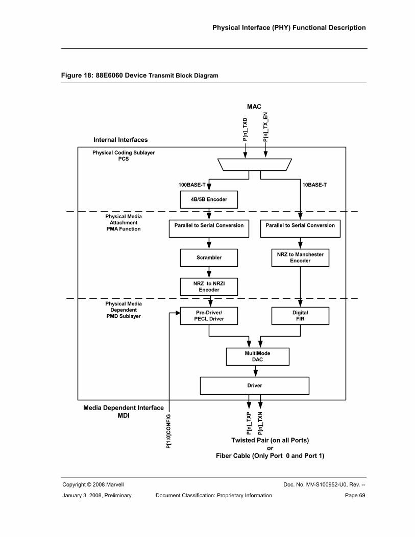
Physical Interface (PHY) Functional Description
Copyright © 2008 Marvell Doc. No. MV-S100952-U0, Rev. --
January 3, 2008, Preliminary Document Classification: Proprietary Information Page 69
Figure 18: 88E6060 Device Transmit Block Diagram
MAC
Pre-Driver/PECL Driver
4B/5B Encoder
MultiModeDAC
Physical Coding SublayerPCS
Physical MediaAttachment
PMA Function
Physical MediaDependent
PMD Sublayer
Parallel to Serial Conversion
Internal Interfaces
Twisted Pair (on all Ports)or
Fiber Cable (Only Port 0 and Port 1)
Driver
P[n]
_TXP
P[n]
_TXN
Media Dependent InterfaceMDI
NRZ to NRZIEncoder
Scrambler
Parallel to Serial Conversion
DigitalFIR
NRZ to ManchesterEncoder
100BASE-T 10BASE-T
P[n]
_TX_
EN
P[1:
0]C
ON
FIG
P[n]
_TXD

Link Street® 88E6060 - UnrestrictedLow Power, 6-port, 10/100 Ethernet Switch
Doc. No. MV-S100952-U0, Rev. -- Copyright © 2008 Marvell
Page 70 Document Classification: Proprietary Information January 3, 2008, Preliminary
Figure 19: 88E6060 Device Receive Block Diagram
ADC
Digital AdaptiveEqualizer
NRZI to NRZDecoder
Descrambler
4B/5B Decoder
Serial to Parallel ConversionCode Group Alignment
AGC
Sample/Hold
MLT-3 toBinary Decoder
Clock Recovery125MHz
SynchronizingFIFO
10Mbps Receiver
Manchester toNRZ Decoder
Serial to Parallel ConversionSFD Alignment
Baseline WanderCompensation
Physical Coding SublayerPCS
Physical Media AttachmentPMA Function
Physical Media DependentPMD Sublayer
Internal Interfaces
Twisted Pair (on all Ports)or
Fiber Cable (Only Port 0 and Port 1)
P[n]
_CR
S_D
V
P[n]
_RXD
Media Dependent InterfaceMDI
P[x]
_RXP
P[x]
_RXN
PECL Receiver
P[1:
0]_S
DET
100BASE-T 10BASE-T
P[1:
0]C
ON
FIG

Physical Interface (PHY) Functional DescriptionTransmit PCS and PMA
Copyright © 2008 Marvell Doc. No. MV-S100952-U0, Rev. --
January 3, 2008, Preliminary Document Classification: Proprietary Information Page 71
4.1 Transmit PCS and PMA
4.1.1 100BASE-TX TransmitterThe 100BASE-TX transmitter consists of several functional blocks that convert synchronous 4-bit nibble data to a scrambled MLT-3 125 Mbps serial data stream.
4.1.2 4B/5B EncodingFor 100BASE-TX mode, the 4-bit nibble is converted to a 5-bit symbol with /J/K/ start-of-stream delimiters and /T/R/ end-of-stream delimiters inserted as needed. The 5-bit symbol is then serialized and scrambled.
4.1.3 ScramblerIn 100BASE-TX mode, the transmit data stream is scrambled in order to reduce radiated emissions on the twisted pair cable. The data is scrambled by exclusive ORing the NRZ signal with the output of an 11-bit wide linear feed-back shift register (LFSR), which produces a 2047-bit repeating pseudo-random sequence. The scrambler reduces peak emissions by randomly spreading the signal energy over the transmit frequency range and eliminat-ing peaks at certain frequencies.
Note
The enabling and disabling of the scrambler and the far end fault generator are controlled in the same way as for the descrambler detection and far end fault detection on the receive side.
4.1.4 NRZ to NRZI ConversionThe data stream is converted from NRZ to NRZI.
4.1.5 Pre-Driver and Transmit ClockThe 88E6060 device uses an all-digital clock generator circuit to create the various receive and transmit clocks necessary for 100BASE-TX, 100BASE-FX, and 10BASE-T modes of operation.
For 100BASE-TX mode, the transmit data is converted to MLT-3-coded symbols. The digital time base generator (TBG) produces the locked 125 MHz transmit clock.
For 100BASE-FX mode, NRZI data is presented directly to the multimode DAC.
For 10BASE-T mode, the transmit data is converted to Manchester encoding. The digital time base generator (TBG) produces the 10 MHz transmit reference clock as well as the over-sampling clock for 10BASE-T waveshap-ing.
4.1.6 Multimode Transmit DACThe multimode transmit digital to analog converter (DAC) transmits MLT3-coded symbols in 100BASE-TX mode, NRZI symbols in 100BASE-FX mode, and Manchester-coded symbols in 10BASE-T mode. The transmit DAC uti-lizes a direct-drive current driver which is well balanced to produce very low common mode transmit noise.
In 100BASE-TX mode, the multimode transmit DAC performs slew control to minimize high frequency EMI.

Link Street® 88E6060 - UnrestrictedLow Power, 6-port, 10/100 Ethernet Switch
Doc. No. MV-S100952-U0, Rev. -- Copyright © 2008 Marvell
Page 72 Document Classification: Proprietary Information January 3, 2008, Preliminary
In 100BASE-FX mode, the pseudo ECL level is generated through external resistive terminations.
In 10BASE-T mode, the multimode transmit DAC generates the needed pre-equalization waveform. This pre-equalization is achieved by using a digital FIR filter.
4.2 Receive PCS and PMA
4.2.1 10-BASE-T/100BASE-TX ReceiverThe differential RXP and RXN pins are shared by the 100BASE-TX, 100BASE-FX (supported on Port 0 and Port 1) and 10BASE-T receivers.
The 100BASE-TX receiver consists of several functional blocks that convert the scrambled MLT-3 125 Mbps serial data stream to the synchronous 4-bit nibble data presented to the MAC interfaces.
4.2.2 AGC and Baseline WanderIn 100BASE-TX mode, after input to the AGC block, the signal is compensated for baseline wander by means of a digitally controlled Digital to Analog converter (DAC). It automatically removes the DC offset from the received sig-nal before it reaches the input to the sample and hold stage of the ADC.
4.2.3 ADC and Digital Adaptive EqualizerIn 100BASE-T mode, an analog to digital converter (ADC) samples and quantizes the input analog signal and sends the result into the digital adaptive equalizer. This equalizer removes inter-symbol interference at the receiver. The digital adaptive equalizer takes unequalized signals from the ADC output and uses a combination of feed-forward equalizer (FFE) and decision feedback equalizer (DFE) for the best optimized signal-to-noise (SNR) ratio.
4.2.4 Digital Phased Locked Loop (DPLL)In 100BASE-TX mode, the receive clock is locked to the incoming data stream and extracts a 125 MHz reference clock. The input data stream is quantized by the recovered clock and sent through to the digital adaptive equalizer from each port.
Digital interpolator clock recovery circuits are optimized for MLT-3, NRZI, and Manchester modes. A digital approach makes the 88E6060 receiver path robust in the presence of variations in process, temperature, on-chip noise, and supply voltage.
4.2.5 NRZI to NRZ ConversionIn 100BASE-TX mode, the recovered 100BASE-TX NRZI signal from the receiver is converted to NRZ data, descrambled, aligned, parallelized, and 5B/4B decoded.
4.2.6 DescramblerThe descrambler is initially enabled upon hardware reset if 100BASE-TX is selected. The scrambler can be enabled or disabled via software by setting the descrambler bit (Table 71).

Physical Interface (PHY) Functional DescriptionReceive PCS and PMA
Copyright © 2008 Marvell Doc. No. MV-S100952-U0, Rev. --
January 3, 2008, Preliminary Document Classification: Proprietary Information Page 73
The descrambler “locks” to the descrambler state after detecting a sufficient number of consecutive idle code-groups. The receiver does not attempt to decode the data stream unless the descrambler is locked. Once locked, the descrambler continuously monitors the data stream to make sure that it has not lost synchronization.
The receiver descrambles the incoming data stream by exclusive ORing it with the output of an 11-bit wide linear feedback shift register (LFSR), which produces a 2047-bit non-repeating sequence.
The descrambler is always forced into the “unlocked” state when a link failure condition is detected or when insuf-ficient idle symbols are detected.
4.2.7 Serial-to-Parallel Conversion and 5B/4B Code-Group Alignment
The Serial-to-Parallel /Symbol Alignment block performs serial to parallel conversion and aligns 5B code-groups to a nibble boundary.
4.2.8 5B/4B DecoderThe 5B/4B decoder translates 5B code-groups into 4B nibbles to be presented to the MAC interfaces. The 5B/4B code mapping is shown in Table 29.
4.2.8.1 FIFOThe 100BASE-X or 10BASE-T packet is placed into the FIFO in order to correct for any clock mismatch between the recovered clock and the reference clock REFCLK.
4.2.8.2 100BASE-FX Receiver In 100BASE-FX mode, a pseudo-ECL (PECL) receiver is used to decode the incoming NRZI signal passed to the NRZI-NRZ decoder. The NRZI signal from the receiver is converted to NRZ data, aligned, parallelized, and 5B/4B decoded as in the 100BASE-TX mode.
4.2.8.3 Far End Fault Indication (FEFI)When 100BASE-FX is selected and Bit 0 of CONFIG_A is low at hardware reset, the far end fault detect (FEFD) circuit is enabled. The FEFD enable state can be overridden by programming the FEFI bit (Table 71).
Note
The FEFI function is always disabled if 100BASE-TX is selected.
4.2.8.4 10BASE-T ReceiverIn 10BASE-T mode, the recovered 10BASE-T signal is decoded from Manchester to NRZ and then aligned. The alignment is necessary to ensure that the start of frame delimiter (SFD) is aligned to the nibble boundary.
In 10BASE-T mode, a receiver is used to decode the differential voltage offset of the Manchester data. Carrier sense is decoded by measuring the magnitude of the voltage offset.
In this mode, the recovered 10BASE-T signal is decoded from Manchester to NRZ data. The data stream is con-verted from serial to parallel format and aligned. The alignment is necessary to ensure that the start of frame delimiter (SFD) is aligned to a byte or nibble boundary. For cable lengths greater than 100 meters, the incoming signal has more attenuation. Hence, the receive voltage threshold should be lowered via the ExtendedDistance bit in the PHY Specific Control Register (Table 71).

Link Street® 88E6060 - UnrestrictedLow Power, 6-port, 10/100 Ethernet Switch
Doc. No. MV-S100952-U0, Rev. -- Copyright © 2008 Marvell
Page 74 Document Classification: Proprietary Information January 3, 2008, Preliminary
Table 29: 5B/4B Code Mapping
PCS Code-Group [4:0]4 3 2 1 0
Name TXD/RXD<3:0>3 2 1 0
Interpretation
1 1 1 1 0 0 0 0 0 0 Data 0
0 1 0 0 1 1 0 0 0 1 Data 1
1 0 1 0 0 2 0 0 1 0 Data 2
1 0 1 0 1 3 0 0 1 1 Data 3
0 1 0 1 0 4 0 1 0 0 Data 4
0 1 1 1 0 6 0 1 1 0 Data 6
0 1 1 1 1 7 0 1 1 1 Data 7
1 0 0 1 0 8 1 0 0 0 Data 8
1 0 0 1 1 9 1 0 0 1 Data 9
1 0 1 1 0 A 1 0 1 0 Data A
1 0 1 1 1 B 1 0 1 1 Data B
1 1 0 1 0 C 1 1 0 0 Data C
1 1 0 1 1 D 1 1 0 1 Data D
1 1 1 0 0 E 1 1 1 0 Data E
1 1 1 0 1 F 1 1 1 1 Data F
1 1 1 1 1 I Undefined IDLE; used as inter-stream fill code
1 1 0 0 0 J 0 1 0 1 Start-of-Stream Delimiter, Part 1 of 2; always used in pairs with K
1 0 0 0 1 K 0 1 0 1 Start-of-Stream Delimiter, Part 2 of 2; always used in pairs with J
0 1 1 0 1 T Undefined End-of-Stream Delimiter, Part 1 of 2; always used in pairs with R
0 0 1 1 1 R Undefined End-of-Stream Delimiter, Part 2 of 2; always used in pairs with T
0 0 1 0 0 H Undefined Transmit Error; used to force signaling errors
0 0 0 0 0 V Undefined Invalid code
0 0 0 0 1 V Undefined Invalid code
0 0 0 1 0 V Undefined Invalid code
0 0 0 1 1 V Undefined Invalid code
0 0 1 0 1 V Undefined Invalid code
0 0 1 1 0 V Undefined Invalid code
0 1 0 0 0 V Undefined Invalid code
0 1 1 0 0 V Undefined Invalid code
1 0 0 0 0 V Undefined Invalid code
1 1 0 0 1 V Undefined Invalid code

Physical Interface (PHY) Functional DescriptionReceive PCS and PMA
Copyright © 2008 Marvell Doc. No. MV-S100952-U0, Rev. --
January 3, 2008, Preliminary Document Classification: Proprietary Information Page 75
4.2.9 Setting Cable CharacteristicsSince cable characteristics differ between unshielded twisted pair and shielded twisted pair cable, optimal receiver performance can be obtained in 100BASE-TX and 10BASE-T modes by setting the TPSelect bit in the PHY Spe-cific Control Register (Table 71) for cable type.
4.2.10 Scrambler/DescramblerThe scrambler block is initially enabled upon hardware reset if 100BASE-TX is selected. If 100BASE-FX or 10BASE-T is selected, the scrambler is disabled by default. The scrambler is controlled by programming the DisS-crambler bit in the PHY Specific Control Register (Table 71).
The scrambler setting is also controlled by hardware configuration at the end of hardware reset. Table 30 shows the effect of various configuration settings on the scrambler.
4.2.11 Digital Clock Recovery/GeneratorThe 88E6060 device uses an all-digital clock recovery and generator circuit to create all of the needed receive and transmit clocks. The digital time base generator (TBG) takes the 25 MHz or 50 MHz reference input clock (XTAL_IN) and produces the locked 25 MHz transmit clock for the MAC in 100BASE-TX mode. It produces a 2.5 MHz transmit clock for the MAC in 10BASE-T mode as well as producing the over-sample clock for 10BASE-T waveshaping.
4.2.12 Link MonitorThe link monitor is responsible for determining whether link is established with a link partner.
In 10BASE-T mode, link monitor function is performed by detecting the presence of the valid link pulses on the RXP/N pins.
In 100BASE-TX mode, the link is established by scrambled idles.
In 100BASE-FX mode, the external fiber-optic receiver performs the signal detection function and communicates this information with the 88E6060 device through SDET pin for Port 0 and Port 1.
If Force Link Good is asserted (ForceLink bit is set high - PHY Specific Control Register, Table 71), the link is forced to be good, and the link monitor is bypassed. Pulse checking is disabled if Auto-Negotiation is disabled, and DisNLPCheck (PHY Specific Control Register, Table 71) is set high. If Auto-Negotiation is disabled and DisN-LPGen (PHY Specific Control Register, Table 71) is set high, then the link pulse transmission is disabled.
Table 30: Scrambler Settings
P[1:0]_CONFIG(If FX is selected)
DisScrambler Bit ( ) Scrambler/ Descrambler
High HW reset to 1 Disabled
Low HW reset to 0 Enabled
X User set to 1 Disabled
X User set to 0 Enabled

Link Street® 88E6060 - UnrestrictedLow Power, 6-port, 10/100 Ethernet Switch
Doc. No. MV-S100952-U0, Rev. -- Copyright © 2008 Marvell
Page 76 Document Classification: Proprietary Information January 3, 2008, Preliminary
4.2.13 Auto-NegotiationAuto-Negotiation is initiated upon any of the following conditions: • Power up reset• Hardware reset• Software reset (SWReset bit—PHY Control Register, Table 61)• Restart Auto-Negotiation (RestartAneg bit—PHY Control Register, Table 61)• Transition from power down to power up (PwrDwn bit—PHY Control Register, Table 61)• Change from the linkfail state to the link-up stateIf Auto-Negotiation is enabled, the 88E6060 device negotiates with its link partner to determine the speed and duplex mode at which to operate. If the link partner is unable to Auto-Negotiate, the 88E6060 device goes into the parallel detect mode to determine the speed of the link partner. Under parallel detect mode, the duplex mode is fixed at half-duplex.
After hardware reset, Auto-Negotiation can be enabled and disabled via the AnegEn bit (PHY Control Register - Table 61). When Auto-Negotiation is disabled, the speed and duplex can be changed via the SpeedLSB and Duplex bits (PHY Control Register - Table 61), respectively. The abilities that are advertised can be changed via the Auto-Negotiation Advertisement Register (Table 65).
4.2.14 Register UpdateChanges to the AnegEn, SpeedLSB, and Duplex bits (Table 65) do not take effect unless one of the following takes place: • Software reset (SWReset bit - Table 61)• Restart Auto-Negotiation (RestartAneg bit - Table 61)• Transition from power down to power up (PwrDwn bit - Table 61)• Loss of the link
The Auto-Negotiation Advertisement register (Table 65) is internally latched once every time Auto-Negotiation enters the ability detect state in the arbitration state machine. Hence, a write into the Auto-Negotiation Advertise-ment Register has no effect once the 88E6060 device begins to transmit Fast Link Pulses (FLPs). This guaran-tees that a sequence of FLPs transmitted is consistent with one another.
The Next Page Transmit register (Table 69) is internally latched once every time Auto-Negotiation enters the next page exchange state in the arbitration state machine.
4.2.15 Next Page SupportThe 88E6060 device supports the use of next page during Auto-Negotiation. By default, the received base page and next page are stored in the Link Partner Ability register - Base Page (Table 66). The 88E6060 device has an option to write the received next page into the Link Partner Next Page register - Table 70 - (similar to the descrip-tion provided in the IEEE 802.3ab standard) by programming the Reg8NxtPg bit (PHY Specific Control Register - Table 71).
4.2.16 Status RegistersOnce the 88E6060 device completes Auto-Negotiation it updates the various status in the PHY Status (Table 72), Link Partner Ability (Next Page) (Table 67), and Auto-Negotiation Expansion (Table 68) registers. Speed, duplex, page received, and Auto-Negotiation completed status are also available in the PHY Specific Status (Table 72) and PHY Interrupt Status registers (Table 74).

Physical Interface (PHY) Functional DescriptionPower Management
Copyright © 2008 Marvell Doc. No. MV-S100952-U0, Rev. --
January 3, 2008, Preliminary Document Classification: Proprietary Information Page 77
4.3 Power ManagementThe 88E6060 supports advanced power management modes that conserve power.
4.3.1 Low Power ModesTwo low power modes are supported in the 88E6060.
• IEEE 802.3 Clause 22.2.4.1.5 compliant power down • Energy Detect+TM
IEEE 802.3 Clause 22.2.4.1.5 power-down compliance allows for the PHY to be placed in a low-power consump-tion state by register control.
Energy Detect+TM allows the 88E6060 to wake up when energy is detected on the wire with the additional capabil-ity to wake up a link partner. The 10BASE-T link pulses are sent once every second while listening for energy on the line.
4.3.2 MAC Interface and PHY Configuration for Low Power ModesThe 88E6060 has one CONFIG bit (in CONFIG_B - Table 3) dedicated to support the low power modes.
Low power modes are also register programmable. The EDet bit (Table 71) enables the user to turn on Energy Detect+™. When the low power mode is not selected, the PwrDwn bit (Table 61) can be used. If during the energy detect mode, the PHY wakes up and starts operating in normal mode, the EDet bit settings are retained. When the link is lost and energy is no longer detected, the 88E6060 returns to the mode stored in the EDet bit.
Table 31 shows how these modes are entered
.
4.3.3 IEEE Power Down ModeThe standard IEEE power down mode is entered by setting the PwrDwn (Table 61 on page 107) bit equal to one. In this mode, the PHY does not respond to any MAC interface signals except the MDC/MDIO. It also does not respond to any activity on the CAT 5 cable.
In this power down mode, the PHY cannot wake up on its own by detecting activity on the CAT 5 cable. It can only wake up by clearing the PwrDwn bit to 0.
4.3.3.1 Energy Detect +TM
In this mode, the PHY sends out a single 10 Mbps NLP (Normal Link Pulse) every second. If the 88E6060 is in Energy Detect+TM mode, it can wake a connected device and it wakes upon the detection of a connected device. When ENA_EDET is 1, the mode of operation is Energy Detect+TM.
Table 31: Operating Mode Power Consumption
Power Mode Est. Power How to Activate Mode
IEEE Power down See Section 9. PwrDwn bit write (Table 61)
Energy Detect+TM Same as IEEE Power down mode—see Section 9.
Configuration option & register EDet bit write (Table 71)

Link Street® 88E6060 - UnrestrictedLow Power, 6-port, 10/100 Ethernet Switch
Doc. No. MV-S100952-U0, Rev. -- Copyright © 2008 Marvell
Page 78 Document Classification: Proprietary Information January 3, 2008, Preliminary
4.4 Far End Fault Indication (FEFI)Far-end fault indication provides a mechanism for transferring information from the local station to the link partner that a remote fault has occurred in 100BASE-FX mode (Port 0 and Port 1 only).
A remote fault is an error in the link that one station can detect while the other one cannot. An example of this is a disconnected fiber at a station’s transmitter. This station is receiving valid data and detects that the link is good via the link monitor, but is not able to detect that its transmission is not propagating to the other station.
A 100BASE-FX station that detects this remote fault modifies its transmitted idle stream pattern from all ones to a group of 84 ones followed by one zero. This is referred to as the FEFI idle pattern.
The FEFI function is controlled by CONFIG_A connection and the DisFEFI bit (Table 71).
Table 32 shows the various configuration settings affecting the FEFI function on hardware reset.
4.5 Virtual Cable Tester™ The 88E6060 PHY Virtual Cable Tester™ feature uses Time Domain Reflectometry (TDR) to determine the quality of the cables, connectors, and terminations. Some of the possible problems that can be diagnosed include opens, shorts, cable impedance mismatches, bad connectors, termination mismatches, and bad magnetics.
The 88E6060 Switch Core conducts a cable diagnostic test by transmitting a signal of known amplitude (+1V) sequentially along each of the TX and RX pairs of an attached cable. The transmitted signal continues along the cable until it is reflected from a cable imperfection. The magnitude of this echo signal and its return time are shown in the VCT registers (Table 81 and Table 82) on the AmpRfln and DistRfln bits respectively.
Using the information from these registers, the VCT registers (Table 81 and Table 82), the distance to the problem location and the type of problem can be determined. For example, the echo time can be converted to distance using Table 81 and Figure 26 . The polarity and magnitude of the reflection together with the distance indicates the type of discontinuity. For example, a +1V reflection indicates an open close to the PHY and a -1V reflection indi-cates a short close to the PHY.
When the cable diagnostic feature is activated by setting the ENVCT bit to one (Table 81), a pre-determined amount of time elapses before a test pulse is transmitted. This is to ensure that the link partner loses link, so that it stops sending100BASE-TX idles or 10 Mbit data packets. This is necessary to be able to perform the TDR test. The TDR test can be performed either when there is no link partner or when the link partner is Auto-Negotiating or sending 10 Mbit idle link pulses. If the 88E6060 device receives a continuous signal for 125 ms, it declares a test
Table 32: FEFI Select
Pn_CONFIG1
1. "n" in Pn_CONFIG may only take the values "0" or "1"
EN_FEFI(CONFIG_A)
FEFI DisFEFI Bit(Table 71)
Auto-Negotiation X Disabled HW set to 1
10BASE-T X Disabled HW set to 1
100BASE-TX X Disabled HW set to 1
100BASE-FX 0 Disabled HW set to 1
100BASE-FX 1 Enabled HW reset to 0

Physical Interface (PHY) Functional DescriptionAuto MDI/MDIX Crossover
Copyright © 2008 Marvell Doc. No. MV-S100952-U0, Rev. --
January 3, 2008, Preliminary Document Classification: Proprietary Information Page 79
failure because it cannot start the TDR test. In the test failure case, the received data is not valid. The results of the test are also summarized in the VCTTst bits (Table 81 and Table 82).
• 11 = Test fail (The TDR test could not be run for reasons explained above)• 00 = valid test, normal cable (no short or open in cable)• 10 = valid test, open in cable (Impedance > 333 ohms)• 01 = valid test, short in cable (Impedance < 33 ohms)
The definition for shorts and opens is arbitrary and can be user-defined using the information in the VCT registers The impedance mismatch at the location of the discontinuity can also be calculated knowing the magnitude of the echo signal. Refer to the Application Note “Virtual Cable Tester -- How to Use TDR results” for details.
4.6 Auto MDI/MDIX CrossoverThe 88E6060 device automatically determines whether or not it needs to interchange cable sense between pairs so that an external crossover cable is not required. If the 88E6060 device interoperates with a device that cannot automatically correct for crossover, the 88E6060 PHY makes the necessary adjustment prior to commencing Auto-Negotiation. If the 88E6060 device interoperates with a device that implements MDI/MDIX crossover, a ran-dom algorithm as described in IEEE 802.3 section 40.4.4 determines which device performs the crossover.
When the 88E6060 device interoperates with legacy 10BASE-T devices that do not implement Auto-Negotiation, it follows the same algorithm as described above since link pulses are present. However, when interoperating with legacy 100BASE-TX devices that do not implement Auto-Negotiation (i.e. link pulses are not present), the 88E6060 device uses signal detection to determine whether to implement crossover.
The Auto MDI/MDIX crossover function can be disabled via the AutoMDI[X] bits (Table 71).
The 88E6060 device is set to normal mode by default if auto MDI/MDIX crossover is disabled at hardware reset.
The pin mapping in normal and crossed modes is specified in Table 33.
Table 33: MDI/MDIX Pin Functions
Physical Pin Normal Crossed
100BASE-TX 10BASE-T 100BASE-TX 10BASE-T
TXP/TXN Transmit Transmit Receive Receive
RXP/RXN Receive Receive Transmit Transmit

Link Street® 88E6060 - UnrestrictedLow Power, 6-port, 10/100 Ethernet Switch
Doc. No. MV-S100952-U0, Rev. -- Copyright © 2008 Marvell
Page 80 Document Classification: Proprietary Information January 3, 2008, Preliminary
4.7 LED InterfaceThe LED interface pins can either be controlled by a port’s PHY or controlled directly, independently of the state of the PHY. Four display options are available and both interfaces (PHY or direct control) can be used together to provide even more LED combinations.
The LEDs can be controlled through a parallel interface or via a serial interface that supports up to seven LEDs per port.
Direct control of the parallel LEDs is achieved by writing to the PHY Manual LED Override register (Table 80). Any of the parallel LEDs can be turned on, off, or made to blink at variable rates independent of the state of the PHY.
When the parallel LEDs are controlled by a port’s PHY, their activity is determined by the PHY’s state. Each LED can be programmed to indicate various PHY states, with variable blink rate.
Some port PHY events configured to drive LED pins are too short to result in an observable change in LED state. For these events, pulse stretching is provided to translate a short PHY event into an observable LED response. The duration of a pulse stretch can be programmed via the PulseStretch bits (Table 79). The default pulse stretch duration is set to 170 to 340 ms. The pulse stretch duration applies to all applicable LED interface pins.
Some of the status indicators signal multiple events by toggling LED interface pins resulting in a blinking LED. The blink period can be programmed via the BlinkRate bits (Table 79). The default blink period is set to 84 ms. The blink rate information is true for all applicable LEDs.
4.7.1 Parallel LED InterfaceThese LED interface pins can be used to display port status information. The LED interface has three different sta-tus indicators for each port with four different default display options, using the Px_LED2, Px_LED1, and Px_LED0 pins.The LED Parallel Select Register (Table 77) specifies which single LED mode status to display on the LED interface pins. The default display for each mode is shown in Table 34 and the default mode that applies depends upon the hardware configuration established using the CONFIG_A pin—see Table 3.
Table 34: Parallel LED Hardware Defaults
LED Mode—set by CONFIG_A at reset
P[4:0]_LED2 P[4:0]_LED1 P[4:0]_LED0
0 LINK RX TX
1 LINK ACT SPEED
2 LINK/RX TX SPEED
3 LINK/ACT DUPLEX/COLX SPEED

Physical Interface (PHY) Functional DescriptionLED Interface
Copyright © 2008 Marvell Doc. No. MV-S100952-U0, Rev. --
January 3, 2008, Preliminary Document Classification: Proprietary Information Page 81
Table 77 shows additional display modes that can be set up by software after startup. Table 35 defines all the pos-sible Parallel LED Display modes.
Table 35: Parallel LED Display Interpretation
Status DescriptionCOLX Low = Collision activity
High = No collision activityThis status is pulse stretched to 170 ms.
ERROR Low = Jabber, received error, false carrier, or FIFO over/underflow occurredHigh = None of the above occurredThis status is pulse stretched to 170 ms.
DUPLEX Low = Full-duplexHigh = Half-duplex
DUPLEX/COLX Low = Full-duplexHigh = Half-duplexBlink = Collision activity (blink rate is 84ms active then 84 ms inactive)The collision activity is pulse stretched to 84 ms.
SPEED Low = Speed is 100 MbpsHigh = Speed is 10 Mbps
LINK Low = Link upHigh = Link down
TX Low = Transmit activityHigh = No transmit activityThis status is pulse stretched to 170 ms.
RX Low = Receive activityHigh = No receive activityThis status is pulse stretched to 170 ms.
ACT Low = Transmit or received activityHigh = No transmit or receive activityThis status is pulse stretched to 170 ms.
LINK/RX Low = Link upHigh = Link downBlink = receive activity (blink rate is 84 ms active then 84ms inactive)The receive activity is pulse stretched to 84 ms.
ACT (blink mode) High = No transmit or receive activityBlink = Transmit or receive activity (blink rate is 84ms active then 84 ms inactive)The transmit and receive activity is pulse stretched to 84 ms.

Link Street® 88E6060 - UnrestrictedLow Power, 6-port, 10/100 Ethernet Switch
Doc. No. MV-S100952-U0, Rev. -- Copyright © 2008 Marvell
Page 82 Document Classification: Proprietary Information January 3, 2008, Preliminary
4.7.2 Serial LED InterfaceThe LEDSER, LEDENA, and LEDCLK pins are used for the serial interface. The CONFIG_A pin (see Table 3) is used to select one of four possible default LED modes which are numerically the same as those set up by the CONFIG_A pin in the parallel case.
However, the default displays in this case are different. The serial LED interface can display a variety of different status indications in 100BASE-TX and 10BASE-T modes (see Table 37 and Table 38). Status to display, pulse stretching, and blink speed can be programmed via the LED Stream Select for Serial LEDs register (Table 78)
4.7.2.1 Single and Dual LED ModesSingle LED mode is initiated at power up according to the CONFIG_A pin settings. Dual LED mode can be entered (or single mode can be reentered) by setting the appropriate register fields according to Table 78. These registers enable LED functions to be programmed individually in dual LED or single LED mode. The data states are sent out on the LEDSER data stream and may be extracted using the LEDCLK and LEDENA signals as shown in the example of Figure 20.
4.7.2.2 Single LED ModesIn the single LED display mode, the same status is driven on both status 100 and status 10 positions in the bit stream. However, the LEDENA signal asserts only over the status that is set and de-asserts over the other posi-tion that is turned off in the bit stream. For example, DUPLEX shows the same status for DUPLEX100 and DUPLEX10. However, the LEDENA signal is high over Duplex100 position only for one clock period. Refer to Figure 20 for more details.
4.7.2.3 Dual LED Display ModeIn the dual LED display mode, two LEDs are used: one for 10 Mbps, and one for 100 Mbps activity. A different sta-tus is driven on status 100 and status 10 positions in the bit stream. In this case, the LEDENA signal asserts overboth 100 and 10 positions in this stream. For example, the LEDENA signal asserts over COLX100 and COLX10 inFigure 20. and remains high for two clock periods. If one of these status bits (shown in Table 38) is turned off,LEDENA is not asserted in both positions.
Figure 20: Serial LEDENA High Clocking with COLX in Dual Mode, Error Off, and DUPLEX in Single Mode
COLX100 COLX10
LEDCLK
80 ns
ERROR
80 ns 160 ns
DUPLEX
160 ns
Dual Led ModeLEDENA High
OFFLEDENA not asserted
Single Led ModeLEDENA assertedonly 1 clock period
LEDENA
LEDSER

Physical Interface (PHY) Functional DescriptionLED Interface
Copyright © 2008 Marvell Doc. No. MV-S100952-U0, Rev. --
January 3, 2008, Preliminary Document Classification: Proprietary Information Page 83
The bit stream on LEDSER can be clocked into a shift register with LEDENA as the shift enable signal as shown in Figure 21. The rate of update of the serial LED interface is controlled by programming register 24.8:6. The default value is set to 42 ms.
Figure 21: Serial LED Conversion
After the LED data is shifted into the correct position, the shift sequence is suspended to allow the appropriate LEDs to light or extinguish depending on status. The LED implementation used in the 88E6060 device is self-syn-chronizing. The default display options are given in Table 36.
The LED status bits are output in the order shown on the LEDSER pin synchronously with LEDCLK. All status sig-nals for Port 5 are sent out first followed by those for Ports 4 through 0. Each bit in the stream occupies a period of80 ns.
Figure 22: Serial LED Display Order—(if all are selected)
Table 37 and Table 38 show the status events that can be displayed by programming the 88E6060 device in single and dual LED display modes.
Table 36: Serial LED Display Options (A = Active)
LEDMode
COLX ERROR DUPLEX DUPLEX/COLX
SPEED LINK TX RX ACT LINK/RX
LINK/ACT
0 - A - A A - - - - - A
1 A A A - A - A - - A -
2 A A A - A A - - A - -
3 A A A - A A A A - - -
<COLX100> → <COLX10> → <ERROR100> → <ERROR10> → <DUPLEX100> → <DUPLEX10>→ <DUPLEX/COLX100> → <DUPLEX/COLX10> → <SPEED100> → <SPEED10> → <LINK100>→ <LINK10> → <TX100> → <TX10> → <RX100> → <RX10> → <ACT100> → <ACT10> → <LINK/RX100>→ <LINK/RX10> → <LINK/ACT100> → <LINK/ACT10>
ShiftRegister
LEDSERLEDENALEDCLK
INENA

Link Street® 88E6060 - UnrestrictedLow Power, 6-port, 10/100 Ethernet Switch
Doc. No. MV-S100952-U0, Rev. -- Copyright © 2008 Marvell
Page 84 Document Classification: Proprietary Information January 3, 2008, Preliminary
4.7.2.4 Single LED Display Mode
Table 37: Single LED Display Mode
Status DescriptionCOLX Low = Collision activity
High = No collision activityThis status has a default pulse stretch duration of 170 ms.
ERROR Low = Jabber, received error, false carrier, or FIFO over/underflow occurredHigh = None of the above occurredThis status has a default pulse stretch duration of 170 ms.
DUPLEX Low = Full-duplexHigh = Half-duplex
DUPLEX/COLX Low = Full-duplexHigh = Half-duplexBlink = Collision activity (blink rate is 84 ms active then 84 ms inactive)The collision activity is pulse stretched to 84 ms.
SPEED Low = Speed is 100 MbpsHigh = Speed is 10 Mbps
LINK Low = Link upHigh = Link down
TX Low = Transmit activityHigh = No transmit activityThis status is pulse stretched to 170 ms.
RX Low = Receive activityHigh = No receive activityThis status is pulse stretched to 170 ms.
ACT Low = Transmit or received activityHigh = No transmit or receive activityThis status is pulse stretched to 170 ms.
LINK/RX Low = Link upHigh = Link downBlink = Receive activity (blink rate is 84 ms active then 84 ms inactive)The receive activity is pulse stretched to 84 ms.
LINK/ACT Low = Link upHigh = Link downBlink = Transmit or receive activity (blink rate is 84ms active then 84 ms inactive)The transmit and receive activity is pulse stretched to 170 ms.

Physical Interface (PHY) Functional DescriptionLED Interface
Copyright © 2008 Marvell Doc. No. MV-S100952-U0, Rev. --
January 3, 2008, Preliminary Document Classification: Proprietary Information Page 85
4.7.2.5 Dual LED Display Mode
Table 38: Dual LED Display Mode
Event DescriptionCOLX100 0 = 100 Mbps collision activity
1 = No 100 Mbps collision activityThis status can be pulse stretched.
COLX10 0 = 10 Mbps collision activity1 = No 10 Mbps collision activityThis status can be pulse stretched.
ERROR100 0 = Received error, false carrier, or 100 Mbps FIFO over/underflow occurred.1 = None of the above occurredThis status can be pulse stretched.
ERROR10 0 = Jabber or 10 Mbps FIFO over/underflow occurred1 = None of the above occurredThis status can be pulse stretched.
DUPLEX100 0 = 100 Mbps full-duplex1 = 100 Mbps half-duplex
DUPLEX10 0 = 10 Mbps full-duplex1 = 10 Mbps half-duplex
DUPLEX/COLX100 0 = 100 Mbps full-duplex1 = Half-duplexBlink = 100 Mbps collision activityThe collision activity can be pulse stretched.The blink rate can be programmed.
DUPLEX/COLX10 0 = 10 Mbps full-duplex1 = 10 Mbps half-duplexBlink = 10 Mbps collision activityThe collision activity can be pulse stretched.The blink rate can be programmed.
SPEED100 0 = Speed is 100 Mbps1 = Speed is 10 Mbps
SPEED10 0 = Speed is 10 Mbps1 = Speed is 100 Mbps
LINK100 0 = 100 Mbps link up1 = 100 Mbps link down
LINK10 0 = 10 Mbps link up1 = 10 Mbps link down
TX100 0 = 100 Mbps transmit activity1 = No 100 Mbps transmit activityThis status can be pulse stretched.
TX10 0 = 10 Mbps transmit activity1 = No 10 Mbps transmit activityThis status can be pulse stretched.
RX100 0 = 100 Mbps receive activity1 = No 100 Mbps receive activityThis status can be pulse stretched.

Link Street® 88E6060 - UnrestrictedLow Power, 6-port, 10/100 Ethernet Switch
Doc. No. MV-S100952-U0, Rev. -- Copyright © 2008 Marvell
Page 86 Document Classification: Proprietary Information January 3, 2008, Preliminary
RX10 0 = 10 Mbps receive activity 1 = No 10 Mbps receive activityThis status can be pulse stretched.
ACT100 0 = 100 Mbps transmit or 100 Mbps receive activity1 = No 100 Mbps transmit or 100 Mbps receive activityThis status can be pulse stretched.
ACT10 0 = 10 Mbps transmit or 10 Mbps receive activity1 = No 10 Mbps transmit or 10 Mbps receive activityThis status can be pulse stretched.
LINK/RX100 0 = 100 Mbps link up1 = 100 Mbps link down Blink = 100 Mbps receive activityThe receive activity can be pulse stretched.The blink rate can be programmed.
LINK/RX10 0 = 10 Mbps link up1 = 10 Mbps link down Blink = 10 Mbps receive activityThe receive activity is can be pulse stretchedThe blink rate can be programmed.
LINK/ACT100 0 = 100 Mbps link up1 = 100 Mbps link downBlink = 100 Mbps transmit or 100 Mbps receive activityThe transmit and receive activity can be pulse stretched.The blink rate can be programmed.
LINK/ACT10 0 = 10 Mbps link up1 = 10 Mbps link down Blink = 10 Mbps transmit or 10 Mbps receive activityThe transmit and receive activity can be pulse stretched.The blink rate can be programmed.
Table 38: Dual LED Display Mode (Continued)
Event Description

Serial Management Interface (SMI)MDC/MDIO Read and Write Operations
Copyright © 2008 Marvell Doc. No. MV-S100952-U0, Rev. --
January 3, 2008, Preliminary Document Classification: Proprietary Information Page 87
Section 5. Serial Management Interface (SMI)
The 88E6060 serial management interface provides access to the internal registers via the MDC and MDIO sig-nals and is compliant with IEEE 802.3u clause 22. MDC is the management data clock input whose frequency can run from DC to a maximum rate of 8.3 MHz. MDIO is the management data input/output which carries a bidirec-tional signal that runs synchronously with the MDC. The MDIO pin requires a pull-up resistor to pull the MDIO high during idle and turnaround times.
5.1 MDC/MDIO Read and Write OperationsAll of the relevant serial management registers, as well as several optional registers, are implemented in the 88E6060 Switch Core. A description of these registers can be found in Section 6. "Switch Register Description" .
Note
Access to the 88E6060 device’s Switch and PHY registers is not possible when the Serial EEPROM is still loading the registers. A CPU can monitor the 88E6060 device INTn pin, which will go active (low) when the Serial EEPROM has been fully processed (i.e., a Halt instruction has been reached - see section 8).

Link Street® 88E6060 - UnrestrictedLow Power, 6-port, 10/100 Ethernet Switch
Doc. No. MV-S100952-U0, Rev. -- Copyright © 2008 Marvell
Page 88 Document Classification: Proprietary Information January 3, 2008, Preliminary
Figure 23: Typical MDC/MDIO Read Operation
Figure 24: Typical MDC/MDIO Write Operation
Table 39 shows an example of a read operation of PHY address 04, register 0, with data of 04C0.Table 39: Serial Management Interface Protocol Example
32-Bit Preamble
Start of Frame
OpcodeRead = 10Write = 01
5-BitPhy
DeviceAddress
5-BitPhy
RegisterAddress
2-BitTurnaroundRead = z0Write = 10
16-BitData Field
Idle
11111111 01 10 00100 00000 z0 0000010011000000 11111111
MDC
MDIO(STA)
0 1 1 0 0 1 1 0 0 0 0 0 0 0 z 0 0 0 0 1 0 0 1 1 0 0 0 0 0 0 0 0z z
MDIO(PHY)
zz
zz
Preamble Start Opcode(Read)
PHY Address Register Address TA Register Data Idle
MDC
MDIO(STA)
0 1 0 1 0 1 1 0 0 0 0 0 0 0 1 0 0 0 0 0 0 0 0 0 0 1 1 0 0 0 0z z
z
Preamble Start Opcode(Write) PHY Address Register Address TA Register Data Idle
0
z

Switch Register Description
Copyright © 2008 Marvell Doc. No. MV-S100952-U0, Rev. --
January 3, 2008, Preliminary Document Classification: Proprietary Information Page 89
Section 6. Switch Register Description
All of the 88E6060 registers are accessible using the IEEE Serial Management Interface (SMI) used for PHY devices (see MDC/MDIO pin description in Section 1 and Section 5 of this datasheet). The 88E6060 device uses 16 of the 32 possible Device Addresses. The16 Device Addresses are configurable at reset by use of the EE_CLK/ADDR4 pin (see Signal Description in part 1 of this datasheet). Figure 25 shows the register map assum-ing the lower 16 SMI Device Addresses are being used.
Figure 25: 88E6060 Register Map
PHY Control
0 1 2 3 4 5 6 7 8 9 A B C D E F
0
1
2
3
4
5
6
7
8
9
A
B
C
D
E
F
10
11
12
13
14
15
16
17
18
19
1A
1B
1C
PHY Status
PHY Identifier
PHY Identifier
Auto-Neg Advertisement
Link Partner Ability
Auto-Neg Expansion
Next Page Transmit
Link Partner Next Page
Reserved
1D
1E
1F
PHY Specific Control 1
PHY Specific Status
PHY Interrupt Enable
PHY Interrupt Status
Interrupt Port Summary
Receive Error Counter
LED Parallel Select
LED Stream Select
LED Control
Reserved
ReservedRx Frame Counter
Tx Frame Counter
Port Status Global Status
Port Control Global Control
Reserved
Reserved
ATU
-MA
C
ATU Operation
Port Based VLAN Map
Res
erve
d
Reserved
Switch Identifier
SMI R
egis
ter A
ddre
ss
SMI Device Address
ATU Control
ATU Data
Sw
itch-
MA
C
Reserved
Free Plus
Port Association Vector
Res
erve
dR
eser
ved
Reserved
LED Override
VCT Control
VCT Status
PHY Specific Control 2

Link Street® 88E6060 - UnrestrictedLow Power, 6-port, 10/100 Ethernet Switch
Doc. No. MV-S100952-U0, Rev. -- Copyright © 2008 Marvell
Page 90 Document Classification: Proprietary Information January 3, 2008, Preliminary
6.1 Register TypesThe registers in the 88E6060 device are made up of one or more fields. The way in which each of these fields operate is defined by the field’s Type. The function of each Type is described in Table 40.
6.2 Switch Core RegistersSwitch Core Registers are of two types:
• Switch Port Registers—are separately configured for each port comprised in the switch. Each port has a unique associated SMI device address and this address is used to access that port’s switch register set.
• Switch Global Registers—are configured using a single SMI device address. A global register’s setting affects all ports of the switch.
The 88E6060 contains six ports (MACS). The supported ports are accessible using SMI device addresses 0x08 to 0x0D, or 0x18 to 0x1D depending upon the value of the EE_CLK/ADDR4 pin at reset (Section 1). The MACs are fully IEEE802.3 compliant. Since there is no IEEE standard covering required MAC registers, these registers are 88E6060 device specific.
The switch contains many global registers that are used to control features and functions that are common to all ports in the switch. The global registers are accessible using SMI device address 0x0F (or 0x1F) depending upon the value of the EE_CLK/ADDR4 pin at reset.
Table 40: Register Types
Type Description
LH Register field with latching high function. If status is high, then the register is set to a one and remains set until a read operation is performed through the management interface or a reset occurs.
LL Register field with latching low function. If status is low, then the register is cleared to a zero and remains cleared until a read operation is performed through the management interface or until a reset occurs.
RES Reserved for future use. All reserved bits are read as zero unless otherwise noted.
RO Read only.
R/W Read and write with no definable initial value
RWR Read/Write reset. All bits are readable and writable. After reset the register field is cleared to zero.
RWS Read/Write set. All bits are readable and writable. After reset the register field is set to a non-zero value specified in the text.
SC Self-Clear. Writing a one to this register causes the required function to be immediately executed, then the register field is cleared to zero when the function is complete.
Update Value written to the register field does not take effect until a soft reset is executed.
Retain Value written to the register field D0
WO Write only. Reads to this type of register field return undefined data.

Switch Register DescriptionSwitch Core Registers
Copyright © 2008 Marvell Doc. No. MV-S100952-U0, Rev. --
January 3, 2008, Preliminary Document Classification: Proprietary Information Page 91
6.2.1 Switch Core Register Map
Table 41: Switch Core Register Map
Description Offset Hex
Offset Decimal
Page Number
Switch Port Registers (SMI Device Address)
Port Status Register 0x00 0 page 92
Reserved Registers 0x01 - 0x02 1 - 2 page 93
Switch Identifier Register 0x03 3 page 93
Port Control Register 0x04 4 page 94
Reserved Registers 0x05 5 page 95
Port Based VLAN Map 0x06 6 page 96
Reserved Registers 0x07 - 0x0A 7 - 10 page 96
Port Association Vector 0x0B 11 page 97
Reserved Registers 0x0C - 0x0F 12 - 15 page 97
Rx Counter 0x10 16 page 98
Tx Counter 0x11 17 page 98
Reserved Registers 0x12 - 0x1F 18 - 31 page 98
Switch Global Registers
Switch Global Status Register 0x00 0 page 99
Switch MAC Address Register Bytes 0 & 1 0x01 1 page 100
Switch MAC Address Register Bytes 2 & 3 0x02 2 page 100
Switch MAC Address Register Bytes 4 & 5 0x03 3 page 100
Switch Global Control Register 0x04 4 page 101
Reserved Registers 0x05 - 0x09 5 - 9 page 101
ATU Control Register 0x0A 10 page 102
ATU Operation Register 0x0B 11 page 103
ATU Data Register 0x0C 12 page 104
ATU MAC Address Register Bytes 0 & 1 0x0D 13 page 104
ATU Switch MAC Address Register Bytes 2 & 3 0x0E 14 page 104
ATU Switch MAC Address Register Bytes 4 & 5 0x0F 15 page 105
Reserved Registers 0x10 - 0x1F 16 - 31 page 105

Link Street® 88E6060 - UnrestrictedLow Power, 6-port, 10/100 Ethernet Switch
Doc. No. MV-S100952-U0, Rev. -- Copyright © 2008 Marvell
Page 92 Document Classification: Proprietary Information January 3, 2008, Preliminary
6.2.2 Switch Port Registers
Table 42: Port Status RegisterOffset: 0x00 (Hex), or 0 (Decimal)
Bits Field Type Description
15 LinkPause RO Link Partner’s Pause bit, returned from the link partner through Auto-Negotia-tion. This bit is valid for Ports with PHYs and when the Resolved bit is set to a one. 0 = MAC Pause not implemented in the link partner 1 = MAC Pause is implemented in the link partner
14 MyPause RO My Pause bit, sent to the link partner during Auto-Negotiation. This bit is valid for Ports with PHYs. It is set high if FD_FLOW_DIS (Section 1) is low during reset. 0 = MAC Pause not implemented in the local MAC 1 = MAC Pause is implemented in the local MAC
13 Resolved RO Link Mode is resolved. 0 = Link is undergoing Auto-Negotiation or the port is disabled 1 = Link has determined its Speed, Duplex and LinkPause settings
12 Link RO Link Status in real time (i.e., it is not latched). 0 = Link is down 1 = Link is up
11 PortMode RO Port mode. The value of this bit is always a one for Ports 0 thru 4 and it comes from Px_MODE3 during configuration for Port 5 and Port 4. 0 = SNI mode is enabled 1 = MII 10/100 or RMII 100 Mbps mode is enabled
10 PHYMode RO PHY mode. This bit is valid for all ports but it is meaningful for Port 5 and Port 4 only and only when the PortMode (bit 11 above) indicates an MII mode of operation (i.e., PortMode is a one). This bit may be either value for SNI con-figured ports – but all SNI port configurations are PHY mode. The value of this bit is always zero for Ports 0 to 3 (and Port 4 if Port 4’s MII is disabled) and it comes from Px_MODE2 during configuration for Port 5 and Port 4 (if Port 4’s MII is enabled). 0 = Pins are in MII MAC Mode (i.e., INCLK and OUTCLK are inputs) or the
pins are in RMII PHY Mode (all RMII Modes are PHY mode where INCLK and OUTCLK are outputs).
1 = Pins are in MII PHY Mode (i.e., INCLK and OUTCLK are output)
9 Duplex RO
R/W on Port 4 & 5 Only
Duplex mode. This bit is valid when the Resolved bit is set to a one. 0 = Half-duplex 1 = Full-duplexThis bit can be written to on Port 5 and Port 4 only so that the Port’s duplex can be modified after Reset occurs. Care must be taken to ensure this Port’s duplex matches the duplex of its link partner.

Switch Register DescriptionSwitch Core Registers
Copyright © 2008 Marvell Doc. No. MV-S100952-U0, Rev. --
January 3, 2008, Preliminary Document Classification: Proprietary Information Page 93
The PortMode, PHYMode, Duplex, and Speed bits for Port 5 and Port 4 come from the Px_MODE[3:0] pins at reset (if Port 4 is in MII mode). When the PortMode is a one, the PHYMode, Duplex, and Speed bits map the same as the other 10/100 ports that contain PHYs. When the PortMode is a zero the mapping is easier to see by looking at "RMII/MII/SNI Configuration" Table 19:.
Note
Registers 0x01 and 0x02 (Hex), or 1 and 2 (Decimal) are reserved.
8 Speed RO Speed mode. This bit is valid when the Resolved bit is set to a one and the PortMode (bit 11 above) is also a one. If the PortMode bit is a zero then the port’s speed is 10 Mbps regardless of the value of this bit. When the port is configured in MII MAC mode, the Speed bit is undefined. 0 = 10 Mbps 1 = 100 Mbps
7:0 Reserved RES Reserved for future use.
Table 43: Switch Identifier RegisterOffset: 0x03 (Hex), or 3 (Decimal)
Bits Field Type Description
15:4 DeviceID RO Device Identifier. The 88E6060 is identified by the value 0x060.
3:0 RevID RO Revision Identifier. The initial version of the 88E6060 has a RevID of 0x0. This RevID field may change at any time. Contact a Marvell FAE for current information on the device revision identifier.
Table 42: Port Status Register (Continued)Offset: 0x00 (Hex), or 0 (Decimal)
Bits Field Type Description

Link Street® 88E6060 - UnrestrictedLow Power, 6-port, 10/100 Ethernet Switch
Doc. No. MV-S100952-U0, Rev. -- Copyright © 2008 Marvell
Page 94 Document Classification: Proprietary Information January 3, 2008, Preliminary
Table 44: Port Control RegisterOffset: 0x04 (Hex), or 4 (Decimal)
Bits Field Type Description
15 ForceFlow Control
RWR Force Flow Control. This bit is used to enable full-duplex flow control or half-duplex back pressure on this port depending upon the port’s current duplex. This bit can only be changed when the port is in the Disabled Port state (bits 1:0 below). 0 = Use configuration pin settings for flow control/back pressure 1 = Force flow control/back pressure to be enabled on this port
14 Trailer RWR Egress Trailer Mode (Port 4 and 5 only). 0 = Normal mode – frames are transmitted unmodified 1 = Add a Trailer to all frames transmitted out of the port.Egress Trailer mode is intended for management CPU ports for source port information on BPDU frame.
13:12 Reserved RES Reserved for future use.
11 Header RWR The detailed information regarding this feature requires an NDA with Marvell® Semiconductor. Please contact your local Marvell Sales Represen-tative for more information.
10:9 Reserved RES Reserved for future use.
8 IngressMode
RWR Ingress Mode (Port 4 and 5 only). 0 = Normal mode – frames are received unmodified 1 = CPU Port with Ingress Trailer mode – frames must be received with a Trailer and the Trailer is checked, potentially used and then removed from the frame.Trailer mode is intended for Ingress data control from a management CPU port so that BPDU frames can be directed.
7 VLANTunnel
RWR VLAN Tunnel. When this bit is cleared to a zero, the VLANs defined in the VLANTable (Table 45, on page 96) are enforced for ALL frames. When this bit is set to a one, the VLANTable masking is bypassed for any frame enter-ing this port with a DA that is currently ‘locked’ in the ATU. This includes uni-cast as well as multicast frames.
6:2 Reserved RES Reserved for future use.

Switch Register DescriptionSwitch Core Registers
Copyright © 2008 Marvell Doc. No. MV-S100952-U0, Rev. --
January 3, 2008, Preliminary Document Classification: Proprietary Information Page 95
Note
Register 0x05 (Hex), or 5 (Decimal) is reserved.
1:0 PortState RWR
Or
RWS to 0b11
Port State. These bits are used to manage a port to determine what kind of frames, if any, are allowed to enter or leave a port for simple bridge loop detection or 802.1D Spanning Tree. The state of these bits can be changed at any time without disrupting frames currently in transit. The Port States are:
00 = Disabled. The switch port is completely disabled and it will not receive or transmit any frames. The QC will return any pre-allocated ingress queue buffers when the port is in this mode.
01 = Blocking/Listening. The switch will examine all frames without learning
any SA addresses, and discard all but MGMT frames. MGMT (man-agement) frames are the only kind of frame that can be tunneled through Blocked ports. A MGMT frame is any frame whose multicast DA address appears in the ATU Database with the MGMT Entry State. It will allow MGMT frames only to exit the port. This mode is used for BPDU handling for bridge loop detection and Spanning Tree support.
10 = Learning. The switch will examine all frames, learning all SA addresses,
and still discard all but MGMT frames. It will allow MGMT frames only to exit the port.
11 = Forwarding. The switch will examine all frames, learning all SA
addresses, and receive and transmit all frames like a normal switch.
The PortState bits for all ports come up in the Forwarding state unless the SW_MODE[1:0] pins are set to 0b00, the CPU attached mode.
Software Reset, (SWReset - Table 54 on page 102) causes the PortState bits to revert back to their reset state (i.e., either Disabled or Forwarding).
Table 44: Port Control Register (Continued)Offset: 0x04 (Hex), or 4 (Decimal)
Bits Field Type Descript ion

Link Street® 88E6060 - UnrestrictedLow Power, 6-port, 10/100 Ethernet Switch
Doc. No. MV-S100952-U0, Rev. -- Copyright © 2008 Marvell
Page 96 Document Classification: Proprietary Information January 3, 2008, Preliminary
,
Note
Registers 0x07 - 0x0A (Hex), or 7 - 10 (Decimal) are reserved.
Table 45: Port Based VLAN MapOffset: 0x06 (Hex), or 6 (Decimal)
Bits Field Type/Reset Value
Description
15:12 DBNum RWR Port’s Default DataBase VLAN Number. This field can be used with VLANs to keep each VLAN’s MAC address mapping database separate from the other VLANs. This allows the same MAC address to appear multiple times in the address database (at most one time per VLAN) with a different port mapping per entry. This field should be zero if not being used. It needs to be a unique number for each independent VLAN if used.
11:6 Reserved RES Reserved for future use.
5:0 VLANTable RWS to all ones except for this port’s bit
Port based VLAN Table. The bits in this table are used to restrict which output ports this input port can send frames to. These bits restrict where a port can send frames to (unless a VLANTunnel frame is being received - see Port Control register, Table 44).
To send frames to Port 0, bit 0 of this register must be a one. To send frames to Port 1, bit 1 of this register must be a one, etc. After reset, all ports are accessible since all the other port number bits are set to a one. This Port’s bit will always be zero at reset. This prevents frames exiting the port on which they arrived. This port’s bit can be set to a one in the 88E6060 Switch Core enabling frames to be returned on their ingress port; consequently care should be taken in writing code to control these bits.This register is reset to 0x3E for Port 0 (SMI Device Address 0x8), and it resets to 0x3D for Port 1 (Addr 0x9) and to 0x3B for Port 2 (Addr 0xA), etc.

Switch Register DescriptionSwitch Core Registers
Copyright © 2008 Marvell Doc. No. MV-S100952-U0, Rev. --
January 3, 2008, Preliminary Document Classification: Proprietary Information Page 97
Note
Registers 0x0C - 0x0F (Hex), or 12 - 15 (Decimal) are reserved.
Table 46: Port Association VectorOffset: 0x0B (Hex), or 11 (Decimal)
Bits Field Type Descript ion
15 IngressMonitor
RWR Ingress Monitor enable. When this bit is set to a one ingress port monitoring is enabled on the same ports upon which egress port monitoring is enabled, as defined by the PAV bits below. This is the recommended operation mode for port monitoring.
14:6 Reserved RES Reserved for future use.
5:0 PAV RWS to all zeros except for this port’s bit
Port Association Vector for ATU learning. The value of these bits is used as the port’s DPV on automatic ATU Learning or Entry_State refresh whenever these bits contain a non-zero value. When these bits are all zero automatic Learning and Entry_State refresh is disabled on this port.
For normal switch operation this port’s bit should be the only bit set in the vector. These bits must only be changed when frames are not entering the port (see PortState bits in Port Control – Table 44, on page 94).
The PAV bits can be used to set up an egress port monitor. To configure Port 0 to receive a copy of the frames that exit Port 1, set bit 0 in Port 1’s PAV reg-ister (along with Port 1’s bit). To configure Port 0 to get a copy of the frames that exit Port 2, set bit 0 in Port 2’s PAV register, etc.
The PAV bits can be used to set up an ingress port monitor along with an egress port monitor. To configure Port 0 to receive a copy of the frames that enter Port 1 as well as exit Port 1, set bit 0 in Port 1’s PAV register (along with Port 1’s bit—bit 1) and set the IngressMonitor bit above.
The PAV bits can be used to set up port trunking (along with the VLANTable bits (Table 45 on page 96). For the two ports that form a trunk, set both of the port’s bits in both port’s PAV registers. Then use the VLANTable to isolate the two ports from each other and to steer the traffic from the other ports down the required trunk line of the pair.

Link Street® 88E6060 - UnrestrictedLow Power, 6-port, 10/100 Ethernet Switch
Doc. No. MV-S100952-U0, Rev. -- Copyright © 2008 Marvell
Page 98 Document Classification: Proprietary Information January 3, 2008, Preliminary
Note
Registers 0x12 - 0x1F (Hex), or 18 - 31 (Decimal) are reserved.
Table 47: Rx CounterOffset: 0x10 (Hex), or 16 (Decimal)
Bits Field Type/Reset Value
Descript ion
15:0 RxCtr RO Received Counter. When CtrMode is cleared to a zero (Global Control – Table 53, on page 101) this counter increments each time a good frame enters this port. It does not matter if the frame is switched or discarded by the switch.
When CtrMode is set to a one this counter increments each time an error frame enters this port. An error frame is one that is 64 bytes or greater with a bad CRC (including alignment errors but not dribbles). Fragments and prop-erly formed frames are not counted.
The counter wraps back to zero. The only time this counter does not incre-ment is when this port is Disabled (see PortState, Table 44, on page 94). This register can be cleared by changing the state of the CtrMode bit in the Switch Global Control register (Table 53 on page 101).
Table 48: Tx CounterOffset: 0x11 (Hex), or 17 (Decimal)
Bits Field Type/Reset Value
Descript ion
15:0 TxCtr RO Transmit Counter. When CtrMode is cleared to a zero (see Global Control – Table 53 on page 101) this counter increments each time a frame success-fully exits this port.
When CtrMode is set to a one this counter increments each time a collision occurs during an attempted transmission. It no longer counts all transmitted frames – but only those transmission attempts that resulted in a collision.
The counter wraps back to zero. The only time this counter does not incre-ment is when this port is Disabled (see PortState field of Port Control Regis-ter (Table 44, on page 94). This register can be cleared by changing the state of the CtrMode bit in Global Control (Table 53 on page 101).

Switch Register DescriptionSwitch Core Registers
Copyright © 2008 Marvell Doc. No. MV-S100952-U0, Rev. --
January 3, 2008, Preliminary Document Classification: Proprietary Information Page 99
6.2.3 Switch Global Registers
Table 49: Switch Global Status RegisterOffset: 0x00 (Hex), or 0 (Decimal)
Bits Field Type Descript ion
15:14 Reserved RES Reserved for future use.
13:12 SW_Mode RO Switch Mode. These bits return the value of the SW_MODE[1:0] pins.
11 InitReady RO Switch Ready. This bit is set to a one when all the blocks inside the device have finished their initialization and are ready to accept frames.
10:4 Reserved RES Reserved for future use.
3 ATUFull LH ATU Full Interrupt. This bit is set to a one if the ATU cannot load or learn a new mapping owing to all of the available locations for an address being locked. It is automatically cleared when read. This bit’s being high causes the 88E6060 INTn pin to go low if the ATUFullIntEn bit in GlobalControl (Table 53, on page 101) is set to a one.
2 ATUDone LH ATU Done Interrupt. This bit is set to a one whenever the ATUBusy bit (Table 55, on page 103) changes from a one to a zero. It is automatically cleared when read. This bit’s being high causes the 88E6060 INTn pin to go low if the ATUDoneIntEn bit in Global Control (Table 53, on page 101) is set to a one.
1 PHYInt RO PHY Interrupt. This bit is set to a one when the PHYs interrupt logic has at least one active interrupt. This bit’s being high causes the 88E6060 INTn pin to go low if the PHYIntEn bit in Global Control (Table 53, on page 101) is set to a one.
0 EEInt LH EEPROM Done Interrupt. This bit is set to a one after the EEPROM finishes loading registers, and it is automatically cleared when read. This bit’s being high causes the 88E6060 INTn pin to go low when the EEIntEn bit in Global Control (Table 53 on page 101) is set to a one.

Link Street® 88E6060 - UnrestrictedLow Power, 6-port, 10/100 Ethernet Switch
Doc. No. MV-S100952-U0, Rev. -- Copyright © 2008 Marvell
Page 100 Document Classification: Proprietary Information January 3, 2008, Preliminary
Table 50: Switch MAC Address Register Bytes 0 & 1Offset: 0x01 (Hex), or 1 (Decimal)
Bits Field Type Description
15:9 MACByte0 RWR MAC Address Byte 0 (bits 47:41) is used as the switch’s source address (SA) in transmitted full-duplex Pause frames. Since bit 0 of byte 0 (bit 40) is the multicast bit (it is the 1st bit down the wire) it is always transmitted as a zero, and its value cannot be changed.
8 DiffAddr RWR Different MAC addresses per Port. This bit is used to have all ports transmit the same or different source addresses in full-duplex Pause frames. 0 = All ports transmit the same SA 1 = Each port uses a different SA where bits 47:3 of the MAC address are the same, but bits 2:0 are the port number (Port 0 = 0, Port 1 = 1, and so on.)
7:0 MACByte1 RWR MAC Address Byte 1 (bits 39:32) is used as the switch’s source address (SA) in transmitted full-duplex Pause frames.
Table 51: Switch MAC Address Register Bytes 2 & 3Offset: 0x02 (Hex), or 2 (Decimal)
Bits Field Type Description
15:8 MACByte2 RWR MAC Address Byte 2 (bits 31:24) is used as the switch’s source address (SA) in transmitted full-duplex Pause frames.
7:0 MACByte3 RWR MAC Address Byte 3 (bits 23:16) is used as the switch’s source address (SA) in transmitted full-duplex Pause frames.
Table 52: Switch MAC Address Register Bytes 4 & 5Offset: 0x03 (Hex), or 3 (Decimal)
Bits Field Type Description
15:8 MACByte4 RWR MAC Address Byte 4 (bits 15:8) is used as the switch’s source address (SA) in transmitted full-duplex Pause frames.
7:0 MACByte5 RWR MAC Address Byte 5 (bits 7:0) is used as the switch’s source address (SA) in transmitted full-duplex Pause frames.
Note: Bits 2:0 of this register are ignored when DiffAddr is set to a one.

Switch Register DescriptionSwitch Core Registers
Copyright © 2008 Marvell Doc. No. MV-S100952-U0, Rev. --
January 3, 2008, Preliminary Document Classification: Proprietary Information Page 101
Note
Registers 0x05 - 0x09 (Hex), or 5 - 9 (Decimal) are reserved.
Table 53: Switch Global Control RegisterOffset: 0x04 (Hex), or 4 (Decimal)
Bits Field Type Descript ion
15:14 Reserved RES Reserved for future use.
13 Discard Excessive
RWR Discard frames with Excessive Collisions. When this bit is set to a one frames that encounter 16 consecutive collisions are discarded. When this bit is cleared to a zero Egress frames are never discarded and the backoff range is reset after 16 consecutive collisions on a single frame.
12:11 Reserved RES Reserved for future use.
10 MaxFrameSize
RWR Maximum Frame Size allowed. The Ingress block discards all frames that are less than 64 bytes in size. It also discards all frames that are greater than a certain size as follows: 0 = Max size is 1522 if IEEE 802.3ac tagged, or 1518 if not tagged 1 = Max size is 1536
9 ReLoad SC Reload the registers using the EEPROM. When this bit is set to a one the contents of the external EEPROM are used to load the registers just as if a reset had occurred. When the reload operation is done, this bit is cleared to a zero automatically, and the EEInt interrupt is set.
8 CtrMode RWR Counter Mode. When this bit is set to a one, the Rx counters for all ports (Table 47, on page 98) count Rx errors and the Tx counters for all ports (Table 48, on page 98) count Tx collisions. When this bit is cleared to a zero, the Rx counters for all ports count Rx frames and the Tx counters for all ports count Tx frames.
The Rx counters and the Tx counters for all ports are cleared to a zero whenever this bit changes state (i.e., it transitions from a one to a zero or from a zero to a one).
7:4 Reserved RES Reserved for future use.
3 ATUFullIntEn
RWR ATU Full Interrupt Enable. This bit must be set to a one to allow the ATU Full interrupt to drive the 88E6060 INTn pin low.
2 ATUDoneIntEn
RWR ATU Done Interrupt Enable. This bit must be set to a one to allow the ATU Done interrupt to drive the 88E6060 INTn pin low.
1 PHYIntEn RWR PHY Interrupt Enable. This bit must be set to a one to allow active interrupts enabled in PHY registers 0x12 to drive the 88E6060 INTn pin low.
0 EEIntEn RWS EEPROM Done Interrupt Enable. This bit must be set to a one to allow the EEPROM Done interrupt to drive the 88E6060 INTn pin low.

Link Street® 88E6060 - UnrestrictedLow Power, 6-port, 10/100 Ethernet Switch
Doc. No. MV-S100952-U0, Rev. -- Copyright © 2008 Marvell
Page 102 Document Classification: Proprietary Information January 3, 2008, Preliminary
Table 54: ATU Control RegisterOffset: 0x0A (Hex), or 10 (Decimal)
Bits Field Type Description
15 SWReset SC Switch Software Reset. Writing a one to this bit causes the QC and the MAC state machines in the switch to be reset. Register values are not modified, except for the PortState bits (Table 44 on page 94) and the EEPROM is not re-read. The PHYs and ATU are not affected by this bit. When the reset oper-ation finishes, this bit is cleared to a zero automatically. The reset occurs immediately. To prevent transmission of CRC frames, set all of the ports to the Disabled state (Table 44 on page 94) and wait for 2 ms (i.e., the time for a maximum frame to be transmitted at 10 Mbps) before setting the SWResetbit to a one.
14 LearnDis RWR ATU Learn Disable. 0 = Normal operation, learning is determined by the PortState (Table 44, on
page 94) 1 = Automatic learning is disabled on all ports – CPU ATU loads still work
13:12 ATUSize RWS to 0x2
Address Translation Unit Table Size. The initial size of the ATU database is 1024 entries. The size of the ATU database can be modified at any time, but an ATU reset and a Switch Software Reset (bit 15 above) occurs automati-cally if the new ATUSize is different from the old ATUSize. 00 = 256 Entry Address Database 01 = 512 Entry Address Database 10 = 1024 Entry Address Database = default 11 = Reserved
11:4 AgeTime RWS to 0x13
ATU Age Time. These bits determine the time that each ATU Entry remains valid in the database, since its last access as a Source Address, before being purged. The value in this register times 16 is the age time in seconds. For example: The default value of 0x13 is 19 decimal.19 x 16 = 304 seconds or just over 5 minutes. The minimum age time is 0x1 or 16 seconds. The maximum age time is 0xFF or 4080 seconds or 68 minutes. When the AgeTime is set to 0x0 the Aging function is disabled, and all learned addresses will remain in the database forever.
3:0 Reserved RES Reserved for future use.

Switch Register DescriptionSwitch Core Registers
Copyright © 2008 Marvell Doc. No. MV-S100952-U0, Rev. --
January 3, 2008, Preliminary Document Classification: Proprietary Information Page 103
Table 55: ATU Operation RegisterOffset: 0x0B (Hex), or 11 (Decimal)
Bits Field Type/Reset Value
Description
15 ATUBusy SC Address Translation Unit Busy. This bit must be set to a one to start an ATU operation (see ATUOp below). Since only one ATU operation can be execut-ing at one time, this bit must be zero before setting it to a one. When the requested ATU operation completes, this bit is automatically cleared to a zero. The transition of this bit from a one to a zero can be used to generate an interrupt (Table 49, on page 99).
14:12 ATUOp RWR Address Translation Unit Table Opcode. The 88E6060 device supports the following ATU operations. All of these operations can be executed while frames are transiting through the switch:000 = No Operation001 = Flush All Entries1
010 = Flush all Unlocked Entries2
011 = Load or Purge an Entry3 in a particular DBNum Database100 = Get Next from a particular DBNum Database4
101 = Flush All Entries in a particular DBNum Database110 = Flush All Unlocked Entries in a particular DBNum Database111 = Reserved
1. All frames flood until new addresses are learned.2. An Unlocked entry is any unicast address with an EntryState less than 0xF. 3. An Entry is Loaded if the EntryState (Table 56, on page 104) is non-zero. An Entry is Purged if it exists and if the EntryState is zero.4. A Get Next operation finds the next higher MAC address currently in a particular ATU database (defined by the DBNum field). The
ATUByte[5:0] values (Table 57, on page 104) are used as the address to start from. To find the lowest MAC address set ATUByte[5:0] to ones. When the operation is done ATUByte[5:0] contains the next higher MAC address found. To find the next address simply issue the Get Next opcode again. If ATUByte[5:0] is returned set to all ones, no higher MAC address was found (if EntryState = 0) or the Broadcast Address was found (if EntryState ≠ 0) In either case, the end of the table was reached. To Search for a particular address, perform a Get Next operation using a MAC address with a value one less than the one being searched for.
11:4 Reserved RES Reserved for future use.
3:0 DBNum RWR ATU MAC Address Database Number. If multiple address databases are not being used, these bits must remain zero. If multiple address databases are being used these bits are used to set the required address database number that is to be used on the Database supported commands (ATUOps 0x3, 0x4, 0x5, and 0x6 above).

Link Street® 88E6060 - UnrestrictedLow Power, 6-port, 10/100 Ethernet Switch
Doc. No. MV-S100952-U0, Rev. -- Copyright © 2008 Marvell
Page 104 Document Classification: Proprietary Information January 3, 2008, Preliminary
Table 56: ATU Data RegisterOffset: 0x0C (Hex), or 12 (Decimal)
Bits Field Type Descript ion
15:10 Reserved RES Reserved for future use.
9:4 PortVec RWR Port Vector. These bits are used as the input Port Vector for ATU load oper-ation. It is the resulting Port Vector from the ATU Get Next operation.
3:0 EntryState RWR ATU Entry State. These bits are used as the input Entry State for ATU Load or purge operations. It is the resulting Entry State from the ATU Get Next operation. (See Table 22 for a description of this function.)
Table 57: ATU Switch MAC Address Register Bytes 0 & 1Offset: 0x0D (Hex), or 13 (Decimal)
Bits Field Type Description
15:8 ATUByte0 RWR ATU MAC Address Byte 0 (bits 47:40) is used as the input MAC address for ATU load, purge, or Get Next operations. It is the resulting MAC address from ATU Get Next operation. Bit 0 of byte 0 (bit 40) is the multicast bit (it is the 1st bit down the wire). Any MAC address with the multicast bit set to a one is considered locked by the ATU.
7:0 ATUByte1 RWR ATU MAC Address Byte 1 (bits 39:32) is used as the input MAC address for ATU load, purge, or Get Next operations. It is the resulting MAC address from the ATU Get Next operation.
Table 58: ATU Switch MAC Address Register Bytes 2 & 3Offset: 0x0E (Hex), or 14 (Decimal)
Bits Field Type Description
15:8 ATUByte2 RWR ATU MAC Address Byte 2 (bits 31:24) is used as the input MAC address for ATU load, purge or Get Next operations. It is the resulting MAC address from ATU Get Next operations.
7:0 ATUByte3 RWR ATU MAC Address Byte 3 (bits 23:16) that are used as the input MAC address for ATU load, purge or Get Next operations. It is the resulting MAC address from ATU Get Next operations.

Switch Register DescriptionSwitch Core Registers
Copyright © 2008 Marvell Doc. No. MV-S100952-U0, Rev. --
January 3, 2008, Preliminary Document Classification: Proprietary Information Page 105
Note
Registers 0x10 - 0x1F (Hex), or 16 - 31 (Decimal) are reserved.
Table 59: ATU Switch MAC Address Register Bytes 4 & 5Offset: 0x0F (Hex), or 15 (Decimal)
Bits Field Type Descript ion
15:8 ATUByte4 RWR ATU MAC Address Byte 4 (bits 15:8) is used as the input MAC address for ATU load, purge or Get Next operations. It is the resulting MAC address from ATU Get Next operations.
7:0 ATUByte5 RWR ATU MAC Address Byte 5 (bits 7:0) is used as the input MAC address for ATU load, purge or Get Next operations. It is the resulting MAC address from ATU Get Next operations.

Link Street® 88E6060 - UnrestrictedLow Power, 6-port, 10/100 Ethernet Switch
Doc. No. MV-S100952-U0, Rev. -- Copyright © 2008 Marvell
Page 106 Document Classification: Proprietary Information January 3, 2008, Preliminary
Section 7. PHY Registers
The 88E6060 device contains five physical layer devices (PHYs). These devices are accessible using SMI device addresses 0x00 to 0x04 (or 0x10 to 0x14) depending upon the value of the EE_CLK/ADDR4 pin at reset. The PHYs are fully IEEE 802.3 compliant including their register interface.
The PHYs in the 88E6060 device are identical to those in the Marvell® 88E3082 Octal Transceiver except that there are five transceivers (transceivers 5 to 7 do not exist and are not accessible).
Table 60: PHY Register Map
Description OffsetHex
OffsetDecimal
Page Number
PHY Control Register 0x00 0 page 107
PHY Status Register 0x01 1 page 109
PHY Identifier 0x02 2 page 110
PHY Identifier 0x03 3 page 110
Auto-Negotiation Advertisement Register 0x04 4 page 111
Link Partner Ability Register (Base Page) 0x05 5 page 113
Link Partner Ability Register (Next Page) 0x05 5 page 113
Auto-Negotiation Expansion Register 0x06 6 page 114
Next Page Transmit Register 0x07 7 page 115
Link Partner Next Page Register 0x08 8 page 115
Reserved Registers 0x09-0x0F 9 - 15 page 116
PHY Specific Control Register I 0x10 16 page 116
PHY Specific Status Register 0x11 17 page 119
PHY Interrupt Enable 0x12 18 page 121
PHY Interrupt Status 0x13 19 page 122
PHY Interrupt Port Summary (Common register to all ports) 0x14 20 page 123
PHY Receive Error Counter 0x15 21 page 124
LED Parallel Select Register 0x16 22 page 125
LED Stream Select Register 0x17 23 page 126
PHY LED Control Register 0x18 24 page 128
PHY Manual LED Override Register 0x19 25 page 129
VCT™ Control Register 0x1A 26 page 130
VCT™ Status Register 0x1B 27 page 131
PHY Specific Control Register II 0x1C 28 page 132
Reserved Registers 0x1D to 0x1F 29 - 31 page 132

PHY Registers
Copyright © 2008 Marvell Doc. No. MV-S100952-U0, Rev. --
January 3, 2008, Preliminary Document Classification: Proprietary Information Page 107
Table 61: PHY Control RegisterOffset: 0x00 (Hex), or 0 (Decimal)
Bits Field Mode HWRst
SWRst
Description
15 SWReset SC 0x0 Self Clear
PHY Software ResetWriting a 1 to this bit causes the PHY state machines to be reset. When the reset operation is done, this bit is cleared to 0 automatically. The reset occurs immedi-ately.1 = PHY reset0 = Normal operation
14 Loopback R/W Retain 0 Enable Loopback ModeWhen loopback mode is activated, the transmitter data presented on TXD is looped back to RXD internally. The PHY has to be in forced 10 or 100 Mbps mode. Auto-Negotiation must be disabled.1 = Enable loopback0 = Disable loopback
13 SpeedLSB R/W ANEG[2:0]
Update Speed Selection (LSB) When a speed change occurs, the PHY drops link and tries to determine speed when Auto-Negotiation is on. Speed, Auto-Negotiation enable, and duplex enable take on the values set by ANEG[2:0] on hardware reset. A write to these registers has no effect unless any one of the following also occurs: Software reset is asserted (bit 15) or Power down (bit 11) transitions from power down to nor-mal operation.1 = 100 Mbps0 = 10 Mbps
12 AnegEn R/W ANEG[2:0]
Update Auto-Negotiation EnableSpeed, Auto-Negotiation enable, and duplex enable take on the values set by ANEG[2:0] on hardware reset. A write to these registers has no effect unless any one of the following also occurs:Software reset is asserted (bit 15, above), Power down (bit 11, below), or transitions from power down to normal operation.If the AnegEn bit is set to 0, the speed and duplex bits of the PHY Control Register (Offset 0x00) take effect. If the AnegEn bit is set to 1, speed and duplex advertise-ment is found in the Auto-Negotiation Advertisement Register (Offset 0x04).1 = Enable Auto-Negotiation Process0 = Disable Auto-Negotiation Process

Link Street® 88E6060 - UnrestrictedLow Power, 6-port, 10/100 Ethernet Switch
Doc. No. MV-S100952-U0, Rev. -- Copyright © 2008 Marvell
Page 108 Document Classification: Proprietary Information January 3, 2008, Preliminary
11 PwrDwn R/W 0x0 0x0 Power Down Mode When the port is switched from power down to normal operation, software reset and restart Auto-Negotiation are performed even when bits Reset (bit 15, above) and Restart Auto-Negotiation (bit 9, below) are not set by the user.1 = Power down0 = Normal operation
10 Isolate RO Always 0
Always 0
Isolate Mode Will always be 0. The Isolate function is not available, since full MII is not implemented.0 = Normal operation
9 RestartAneg SC 0x0 Self Clear
Restart Auto-NegotiationAuto-Negotiation automatically restarts after hardware or software reset regardless of whether or not the restart bit is set.1 = Restart Auto-Negotiation Process0 = Normal operation
8 Duplex R/W ANEG[2:0]
Update Duplex Mode SelectionSpeed, Auto-Negotiation enable, and duplex enable take on the values set by ANEG[2:0] on hardware reset. A write to these registers has no effect unless any one of the following also occurs: Software reset is asserted (bit 15), Power down (bit 11), or transitions from power down to normal operation.1 = Full-duplex0 = Half-duplex
7 ColTest RO Always 0
Always 0
Collision Test Mode Will always be 0. The Collision test is not available, since full MII is not implemented.0 = Disable COL signal test
6 SpeedMSB RO Always 0
Always 0
Speed Selection Mode (MSB) Will always be 0.0 = 100 Mbps or 10 Mbps
5:0 Reserved RO Always 0
Always 0
Will always be 0.
Table 61: PHY Control Register (Continued)Offset: 0x00 (Hex), or 0 (Decimal)
Bits Field Mode HWRst
SWRst
Description

PHY Registers
Copyright © 2008 Marvell Doc. No. MV-S100952-U0, Rev. --
January 3, 2008, Preliminary Document Classification: Proprietary Information Page 109
Table 62: PHY Status RegisterOffset: 0x01 (Hex), or 1 (Decimal)
Bits Field Mode HWRst
SWRst
Description
15 100T4 RO Always 0
Always 0
100BASE-T4This protocol is not available.0 = PHY not able to perform 100BASE-T4
14 100FDX RO Always 1
Always 1
100BASE-T and 100BASE-X full-duplex1 = PHY able to perform full-duplex
13 100HDX RO Always 1
Always 1
100BASE-T and 100BASE-X half-duplex1 = PHY able to perform half-duplex
12 10FDX RO Always 1
Always 1
10BASE-T full-duplex1 = PHY able to perform full-duplex
11 10HPX RO Always 1
Always 1
10BASE-T half-duplex1 = PHY able to perform half-duplex
10 100T2FDX RO Always 0
Always 0
100BASE-T2 full-duplex. This protocol is not available.0 = PHY not able to perform full-duplex
9 100T2HDX RO Always 0
Always 0
100BASE-T2 half-duplexThis protocol is not available.0 = PHY not able to perform half-duplex
8 ExtdStatus RO Always 0
Always 0
Extended Status0 = No extended status information in Register 15
7 Reserved RO Always 0
Always 0
Must always be 0.
6 MFPreSup RO Always 1
Always 1
MF Preamble Suppression ModeMust be always 1.1 = PHY accepts management frames with preamble suppressed
5 AnegDone RO 0x0 0 Auto-Negotiation Complete1 = Auto-Negotiation process completed0 = Auto-Negotiation process not completed
4 RemoteFault RO, LH
0x0 0 Remote Fault Mode1 = Remote fault condition detected0 = Remote fault condition not detected
3 AnegAble RO Always 1
Always 1
Auto-Negotiation Ability Mode1 = PHY able to perform Auto-Negotiation

Link Street® 88E6060 - UnrestrictedLow Power, 6-port, 10/100 Ethernet Switch
Doc. No. MV-S100952-U0, Rev. -- Copyright © 2008 Marvell
Page 110 Document Classification: Proprietary Information January 3, 2008, Preliminary
2 Link RO, LL
0x0 0 Link Status ModeThis register indicates when link was lost since the last read. For the current link status, either read this register back-to-back or read RTLink in Table 72 on page 119.1 = Link is up0 = Link is down
1 JabberDet RO, LH
0x0 0 Jabber Detect1 = Jabber condition detected0 = Jabber condition not detected
0 ExtdReg RO Always 1
Always 1
Extended capability mode.1 = Extended register capabilities
Table 63: PHY IdentifierOffset: 0x02 (Hex), or 2 (Decimal)
Bits Field Mode HWRst
SWRst
Description
15:0 OUI MSb RO 0x0141 0x0141 Organizationally Unique Identifier bits 3:18 0000000101000001Marvell® OUI is 0x005043
Table 64: PHY IdentifierOffset: 0x03 (Hex), or 3 (Decimal)
Bits Field Mode HWRst
SWRst
Descript ion
15:10 OUI LSb RO Always 000011
Always 000011
Organizationally Unique Identifier bits19:24
9:4 ModelNum RO Varies Varies Model Number = 001000
3:0 RevNum RO Varies Varies Revision NumberContact Marvell® FAEs for information on the device revision number.
Table 62: PHY Status Register (Continued)Offset: 0x01 (Hex), or 1 (Decimal)
Bits Field Mode HWRst
SWRst
Description

PHY Registers
Copyright © 2008 Marvell Doc. No. MV-S100952-U0, Rev. --
January 3, 2008, Preliminary Document Classification: Proprietary Information Page 111
Table 65: Auto-Negotiation Advertisement RegisterOffset: 0x04 (Hex), or 4 (Decimal)
Bits Field Mode HW Rst
SWRst
Description
15 AnegAd NxtPage
R/W 0x0 Retain Next Page1 = Advertise0 = Not advertisedValues programmed into the Auto-Negotiation Adver-tisement Register have no effect unless Auto-Negotia-tion is restarted (RestartAneg - Table 61 on page 107) or link goes down.
14 Ack RO Always 0
Always 0
Must be 0.
13 AnegAdReFault
R/W 0x0 Retain Remote Fault Mode1 = Set Remote Fault bit0 = Do not set Remote Fault bitValues programmed into the Auto-Negotiation Adver-tisement Register have no effect unless Auto-Negotia-tion is restarted (RestartAneg - Table 61 on page 107) or link goes down.
12:11 Reserved R/W 0x0 Retain Must be 00. Reserved bits are R/W to allow for forward compatibility with future IEEE standards.Values programmed into the Auto-Negotiation Adver-tisement Register have no effect unless Auto-Negotia-tion is restarted (RestartAneg - Table 61 on page 107) or link goes down.
10 AnegAdPause
R/W 0x0 Retain Pause Mode1 = MAC Pause implemented0 = MAC Pause not implementedValues programmed into the Auto-Negotiation Adver-tisement Register have no effect unless Auto-Negotia-tion is restarted (RestartAneg - Table 61 on page 107) or link goes down.
9 AnegAd100T4
RO Always 0
Always 0
100BASE-T4 mode0 = Not capable of 100BASE-T4
8 AnegAd100FDX
R/W 0x1 Retain 100BASE-TX full-duplex Mode1 = Advertise0 = Not advertisedValues programmed into the Auto-Negotiation Adver-tisement Register have no effect unless Auto-Negotia-tion is restarted (RestartAneg - Table 61 on page 107) or link goes down.

Link Street® 88E6060 - UnrestrictedLow Power, 6-port, 10/100 Ethernet Switch
Doc. No. MV-S100952-U0, Rev. -- Copyright © 2008 Marvell
Page 112 Document Classification: Proprietary Information January 3, 2008, Preliminary
7 AnegAd100HDX
R/W 0X1 Retain 100BASE-TX half-duplex Mode1 = Advertise0 = Not advertisedValues programmed into the Auto-Negotiation Adver-tisement Register have no effect unless Auto-Negotia-tion is restarted (RestartAneg - Table 61 on page 107) or link goes down.
6 AnegAd10FDX
R/W 0X1 Retain 10BASE-TX full-duplex Mode1 = Advertise0 = Not advertisedValues programmed into the Auto-Negotiation Adver-tisement Register have no effect unless Auto-Negotia-tion is restarted (RestartAneg - Table 61 on page 107) or link goes down.
5 AnegAd10HDX
R/W 0X1 Retain 10BASE-TX half-duplex Mode1 = Advertise0 = Not advertisedValues programmed into the Auto-Negotiation Adver-tisement Register have no effect unless Auto-Negotia-tion is restarted (RestartAneg - Table 61 on page 107) or link goes down.
4:0 AnegAdSelector
RO Always 0x01
Always 0x01
Selector Field Mode00001 = 802.3
Table 65: Auto-Negotiation Advertisement Register (Continued)Offset: 0x04 (Hex), or 4 (Decimal)
Bits Field Mode HW Rst
SWRst
Descript ion

PHY Registers
Copyright © 2008 Marvell Doc. No. MV-S100952-U0, Rev. --
January 3, 2008, Preliminary Document Classification: Proprietary Information Page 113
Table 66: Link Partner Ability Register (Base Page)Offset: 0x05 (Hex), or 5 (Decimal)
Bits Field Mode HW Rst
SWRst
Descript ion
15 LPNxt Page RO 0x0 0 Next Page ModeBase page will be overwritten if next page is received and if Reg8NxtPg (Table 71 on page 116) is disabled.When Reg8NxtPg (Table 71 on page 116) is enabled, then next page is stored in the Link Partner Next Page register (Table 70 on page 115), and the Link Partner Ability Register (Table 66 on page 113) holds the base page.Received Code Word Bit 15
14 LPAck RO 0x0 0 AcknowledgeReceived Code Word Bit 14
13 LPRemote Fault
RO 0x0 0 Remote FaultReceived Code Word Bit 13
12:5 LPTechAble RO 0x00 0x00 Technology Ability FieldReceived Code Word Bit 12:5
4:0 LPSelector RO 00000 00000 Selector FieldReceived Code Word Bit 4:0
Table 67: Link Partner Ability Register (Next Page)Offset: 0x05 (Hex), or 5 (Decimal)
Bits Field Mode HWRst
SWRst
Descript ion
15 LPNxtPage RO -- -- Next Page ModeBase page will be overwritten if next page is received and if Reg8NxtPg (Table 71 on page 116) is disabled.When Reg8NxtPg (Table 71 on page 116) is enabled, then next page is stored in the Link Partner Next Page register (Table 70 on page 115), and Link Partner Abil-ity Register (Table 66 on page 113) holds the base page.Received Code Word Bit 15
14 LPAck RO -- -- AcknowledgeReceived Code Word Bit 14
13 LPMessage RO -- -- Message PageReceived Code Word Bit 13
12 LPack2 RO -- -- Acknowledge 2Received Code Word Bit 12
11 LPToggle RO -- -- ToggleReceived Code Word Bit 11

Link Street® 88E6060 - UnrestrictedLow Power, 6-port, 10/100 Ethernet Switch
Doc. No. MV-S100952-U0, Rev. -- Copyright © 2008 Marvell
Page 114 Document Classification: Proprietary Information January 3, 2008, Preliminary
10:0 LPData RO -- -- Message/Unformatted FieldReceived Code Word Bit 10:0
Table 68: Auto-Negotiation Expansion RegisterOffset: 0x06 (Hex), or 6 (Decimal)
Bits Field Mode HWRst
SWRst
Descript ion
15:5 Reserved RO Always 0x000
Always0x000
Reserved. Must be 00000000000. The Auto-Negotiation Expansion Register is not valid until the AnegDone (Table 62 on page 109) indicates completed.
4 ParFaultDet RO 0x0 0x0 Parallel Detection Level1 = A fault has been detected via the Parallel Detection function0 = A fault has not been detected via the Parallel Detec-tion function
3 LPNxtPgAble
RO 0x0 0x0 Link Partner Next Page Able1 = Link Partner is Next Page able0 = Link Partner is not Next Page able
2 LocalNxtPgAble
RO Always 0x1
Always 0x1
Local Next Page AbleThis bit is equivalent to AnegAble (Table 62 on page 109).1 = Local Device is Next Page able
1 RxNewPage RO/LH 0x0 0x0 Page Received1 = A New Page has been received0 = A New Page has not been received
0 LPAnegAble RO 0x0 0x0 Link Partner Auto-Negotiation Able 1 = Link Partner is Auto-Negotiation able0 = Link Partner is not Auto-Negotiation able
Table 67: Link Partner Ability Register (Next Page) (Continued)Offset: 0x05 (Hex), or 5 (Decimal)
Bits Field Mode HWRst
SWRst
Description

PHY Registers
Copyright © 2008 Marvell Doc. No. MV-S100952-U0, Rev. --
January 3, 2008, Preliminary Document Classification: Proprietary Information Page 115
Table 69: Next Page Transmit RegisterOffset: 0x07 (Hex), or 7 (Decimal)
Bits Field Mode HWRst
SWRst
Descript ion
15 TxNxtPage R/W 0x0 0x0 Next PageA write to the Next Page Transmit Register implicitly sets a variable in the Auto-Negotiation state machine indicat-ing that the next page has been loaded.Transmit Code Word Bit 15
14 Reserved RO 0x0 0x0 ReservedTransmit Code Word Bit 14
13 TxMessage R/W 0x1 0x1 Message Page ModeTransmit Code Word Bit 13
12 TxAck2 R/W 0x0 0x0 Acknowledge2Transmit Code Word Bit 12
11 TxToggle RO 0x0 0x0 ToggleTransmit Code Word Bit 11
10:0 TxData R/W 0x001 0x001 Message/Unformatted FieldTransmit Code Word Bit 10:0
Table 70: Link Partner Next Page RegisterOffset: 0x08 (Hex), or 8 (Decimal)
Bits Field Mode HWRst
SWRst
Descript ion
15 RxNxtPage RO 0x0 0x0 Next PageIf Reg8NxtPg (Table 71 on page 116) is enabled, then next page is stored in the Link Partner Next Page reg-ister (Table 70 on page 115); otherwise, theLink Part-ner Next Page register (Table 70 on page 115) is cleared to all 0’s.Received Code Word Bit 15
14 RxAck RO 0x0 0x0 AcknowledgeReceived Code Word Bit 14
13 RxMessage RO 0x0 0x0 Message PageReceived Code Word Bit 13
12 RxAck2 RO 0x0 0x0 Acknowledge 2Received Code Word Bit 12
11 RxToggle RO 0x0 0x0 ToggleReceived Code Word Bit 11
10:0 RxData RO 0x001 0x000 Message/Unformatted FieldReceived Code Word Bit 10:0

Link Street® 88E6060 - UnrestrictedLow Power, 6-port, 10/100 Ethernet Switch
Doc. No. MV-S100952-U0, Rev. -- Copyright © 2008 Marvell
Page 116 Document Classification: Proprietary Information January 3, 2008, Preliminary
Note
Registers 0x09 through 0x0F (hexadecimal (9 through 15 decimal) are reserved. Do not read or write to these registers.
Table 71: PHY Specific Control RegisterOffset: 0x10 (Hex), or 16 (Decimal)
Bits Field Mode HWRst
SWRst
Description
15 Reserved RES -- -- Reserved.
14 EDet R/W ENA_EDET
Retain Energy Detect1 = Enable with sense and pulse0 = DisableEnable with sense only is not supportedEnable Energy Detect takes on the appropriate value defined by the CONFIG9 pin at hardware reset.
13 DisNLPCheck
R/W 0x0 0x0 Disable Normal Linkpulse Check Linkpulse check and generation disable have no effect, if Auto-Negotiation is enabled locally.1 = Disable linkpulse check0 = Enable linkpulse check
12 Reg8NxtPg R/W 0x0 0x0 Enable the Link Partner Next Page register (Table 67 on page 113) to store Next Page. If set to store next page in the Link Partner Next Page register (Table 67 on page 113), then 802.3u is violated to emulate 802.3ab.1 = Store next page in the Link Partner Next Page regis-ter (Table 67 on page 113)0 = Store next page in the Link Partner Ability Register (Base Page) register (Table 66 on page 113).
11 DisNLPGen R/W 0x0 0x0 Disable Linkpulse Generation. Linkpulse check and generation disable have no effect, when Auto-Negotiation is enabled locally.1 = Disable linkpulse generation0 = Enable linkpulse generation
10 ForceLink R/W 0x0 0x0 Force Link Good When link is forced to be good, the link state machine is bypassed and the link is always up.1 = Force link good0 = Normal operation
9 DisScrambler R/W ANEG[2:0]
Retain Disable Scrambler If fiber mode is selected then the scrambler is disabled at hardware reset.1 = Disable scrambler0 = Enable scrambler

PHY Registers
Copyright © 2008 Marvell Doc. No. MV-S100952-U0, Rev. --
January 3, 2008, Preliminary Document Classification: Proprietary Information Page 117
8 DisFEFI R/W DIS_FEFI ANEG[2:0]
Retain Disable FEFI In 100BASE-FX mode, Disable FEFI takes on the appro-priate value defined by the CONFIG8 pin at hardware reset. FEFI is automatically disabled regardless of the state of this bit if copper mode is selected.1 = Disable FEFI0 = Enable FEFI
For the 88E3083 device, this bit applies to Port 7 only.
7 ExtdDistance R/W 0x0 0x0 Enable Extended Distance When using cable exceeding 100 meters, the 10BASE-T receive threshold must be lowered in order to detect incoming signals.1 = Lower 10BASE-T receive threshold0 = Normal 10BASE-T receive threshold
6 TPSelect R/W ANEG [2:0]
Update (Un)Shielded Twisted Pair This setting can be changed by writing to this bit fol-lowed by software reset.1 = Shielded Twisted Pair0 = Unshielded Twisted Pair - default
5:4 AutoMDI[X] R/W ENA_XC,1
Update MDI/MDIX Crossover This setting can be changed by writing to these bits fol-lowed by software reset.If ENA_XC is 1 at hardware reset then bits 5:4 = 1100 = Transmit on pins RXP/RXN, Receive on pins TXP/TXN01 = Transmit on pins TXP/TXN, Receive on pins RXP/RXN1x = Enable Automatic Crossover
3:2 RxFIFODepth
R/W 0x0 0x0 Receive FIFO Depth00 = 4 Bytes01 = 6 Bytes10 = 8 Bytes11 = Reserved
1 AutoPol R/W 0x0 00 Polarity Reversal If polarity is disabled, then the polarity is forced to be normal in 10BASE-T mode. Polarity reversal has no effect in 100BASE-TX mode.1 = Disable automatic polarity reversal0 = Enable automatic polarity reversal
Table 71: PHY Specific Control Register (Continued)Offset: 0x10 (Hex), or 16 (Decimal)
Bits Field Mode HWRst
SWRst
Description

Link Street® 88E6060 - UnrestrictedLow Power, 6-port, 10/100 Ethernet Switch
Doc. No. MV-S100952-U0, Rev. -- Copyright © 2008 Marvell
Page 118 Document Classification: Proprietary Information January 3, 2008, Preliminary
0 DisJabber R/W 0x0 00 Disable JabberJabber has no effect in full-duplex or in 100BASE-X mode.1 = Disable jabber function0 = Enable jabber function
Table 71: PHY Specific Control Register (Continued)Offset: 0x10 (Hex), or 16 (Decimal)
Bits Field Mode HWRst
SWRst
Description

PHY Registers
Copyright © 2008 Marvell Doc. No. MV-S100952-U0, Rev. --
January 3, 2008, Preliminary Document Classification: Proprietary Information Page 119
Table 72: PHY Specific Status RegisterOffset: 0x11 (Hex), or 17 (Decimal)
Bits Field Mode HWRst
SWRst
Descript ion
15 Reserved RES -- -- Reserved
14 ResSpeed RO ANEG[2:0]
Retain Resolved Speed Speed and duplex takes on the values set by ANEG[2:0] pins on hardware reset only. The values are updated after the completion of Auto-Negotiation. The registers retain their values during software reset.1 = 100 Mbps0 = 10 Mbps
13 ResDuplex RO ANEG[2:0]
Retain Resolved Duplex ModeSpeed and duplex takes on the values set by ANEG[2:0] pins on hardware reset only. The values are updated after the completion of Auto-Negotiation. The registers retain their values during software reset. This bit is valid only after the resolved bit 11 is set.1 = Full-duplex0 = Half-duplex
12 RcvPage RO, LH
0x0 0x0 Page Receive Mode1 = Page received0 = Page not received
11 Resolved RO 0x0 0x0 Speed and Duplex Resolved. Speed and duplex bits (14 and 13) are valid only after the Resolved bit is set. The Resolved bit is set when Auto-Negotiation is completed or Auto-Negotiation is disabled.1 = Resolved0 = Not resolved
10 RTLink RO 0x0 0x0 Link (real time)1 = Link up0 = Link down
9:7 Reserved RES 0x0 0x0 Must be 000.
6 MDI/MDIX RO 0x1 0x1 MDI/MDIX Crossover Status1 = Transmit on pins RXP/RXN, Receive on pins TXP/TXN0 = Transmit on pins TXP/TXN, Receive on pins RXP/RXN
5 Reserved RES 0x4 0x4 Must be 0.
4 Sleep RO 0 0x0 Energy Detect Status1 = Chip is in sleep mode (No wire activity)0 = Chip is not in sleep mode (Active)
3:2 Reserved RES 0x0 0x0 Must be 00.

Link Street® 88E6060 - UnrestrictedLow Power, 6-port, 10/100 Ethernet Switch
Doc. No. MV-S100952-U0, Rev. -- Copyright © 2008 Marvell
Page 120 Document Classification: Proprietary Information January 3, 2008, Preliminary
1 RTPolarity RO 0x0 0x0 Polarity (real time)1 = Reversed0 = Normal
0 RTJabber RO Retain 0x0 Jabber (real time)1 = Jabber0 = No Jabber
Table 72: PHY Specific Status Register (Continued)Offset: 0x11 (Hex), or 17 (Decimal)
Bits Field Mode HWRst
SWRst
Description

PHY Registers
Copyright © 2008 Marvell Doc. No. MV-S100952-U0, Rev. --
January 3, 2008, Preliminary Document Classification: Proprietary Information Page 121
Table 73: PHY Interrupt EnableOffset: 0x12 (Hex), or 18 (Decimal)
Bits Field Mode HWRst
SWRst
Descript ion
15 Reserved RES -- -- Reserved
14 SpeedIntEn R/W 0x0 Retain Speed Changed Interrupt Enable1 = Interrupt enable0 = Interrupt disable
13 DuplexIntEn R/W 0x0 Retain Duplex Changed Interrupt Enable1 = Interrupt enable0 = Interrupt disable
12 RcvPageIntEn R/W 0x0 Retain Page Received Interrupt Enable1 = Interrupt enable0 = Interrupt disable
11 AnegDoneIntEn
R/W 0x0 Retain Auto-Negotiation Completed Interrupt Enable1 = Interrupt enable0 = Interrupt disable
10 LinkIntEn R/W 0x0 Retain Link Status Changed Interrupt Enable1 = Interrupt enable0 = Interrupt disable
9 SymErrIntEn R/W 0x0 Retain Symbol Error Interrupt Enable1 = Interrupt enable0 = Interrupt disable
8 FlsCrsIntEn R/W 0x0 Retain False Carrier Interrupt Enable1 = Interrupt enable0 = Interrupt disable
7 FIFOErrInt R/W 0x0 Retain FIFO Over/Underflow Interrupt Enable1 = Interrupt enable0 = Interrupt disable
6 MDI[x]IntEn R/W 0x0 0x0 MDI/MDIX Crossover Changed Interrupt Enable1 = Interrupt enable0 = Interrupt disable
5 Reserved RES 0x0 Retain Must be 0.
4 EDetIntEn R/W 0x0 Retain Energy Detect Interrupt Enable1 = Enable0 = Disable
3:2 Reserved RES 0x0 Retain Must be 00.
1 PolarityIntEn R/W 0x0 Retain Polarity Changed Interrupt Enable1 = Interrupt enable0 = Interrupt disable
0 JabberIntEn R/W 0x0 Retain Jabber Interrupt Enable1 = Interrupt enable0 = Interrupt disable

Link Street® 88E6060 - UnrestrictedLow Power, 6-port, 10/100 Ethernet Switch
Doc. No. MV-S100952-U0, Rev. -- Copyright © 2008 Marvell
Page 122 Document Classification: Proprietary Information January 3, 2008, Preliminary
Table 74: PHY Interrupt StatusOffset: 0x13 (Hex), or 19 (Decimal)
Bits Field Mode HWRst
SWRst
Description
15 Reserved RES -- -- Reserved
14 SpeedInt RO, LH
0x0 0x0 Speed Changed1 = Speed changed0 = Speed not changed
13 DuplexInt RO, LH
0x0 0x0 Duplex Changed1 = Duplex changed0 = Duplex not changed
12 RxPageInt RO, LH
0x0 0x0 1 = Page received0 = Page not received
11 AnegDoneInt RO, LH
0x0 0x0 Auto-Negotiation Completed1 = Auto-Negotiation completed0 = Auto-Negotiation not completed
10 LinkInt RO, LH
0x0 0x0 Link Status Changed1 = Link status changed0 = Link status not changed
9 SymErrInt RO, LH
0x0 0x0 Symbol Error1 = Symbol error0 = No symbol error
8 FlsCrsInt RO, LH
0x0 0x0 False Carrier1 = False carrier0 = No false carrier
7 FIFOErrInt RO, LH
0x0 0x0 FIFO Over /Underflow Error1 = Over/underflow error0 = No over/underflow error
6 MDIMDIXInt RO, LH
0x0 0x0 MDI/MDIX Crossover Changed1 = MDI/MDIX crossover changed0 = MDI/MDIX crossover not changed
5 Reserved RO Always 0
Always 0
Must be 0
4 EDetChg RO, LH
0x0 0x0 Energy Detect Changed 1 = Changed0 = No Change
3:2 Reserved RO 0x0 0x0 Must be 00
1 PolarityInt RO 0x0 0x0 Polarity Changed1 = Polarity changed0 = Polarity not changed
0 JabberInt RO, LH
0x0 0x0 Jabber Mode1 = Jabber0 = No Jabber

PHY Registers
Copyright © 2008 Marvell Doc. No. MV-S100952-U0, Rev. --
January 3, 2008, Preliminary Document Classification: Proprietary Information Page 123
Table 75: PHY Interrupt Port Summary (Global1) Offset: 0x14 (Hex), or 20 (Decimal)
1. This global register is accessible for writing or reading from any PHY port (i.e., only one physical register exists for all the PHY Ports).
Bits Field Mode HWRst
SWRst
Descript ion
15:5 Reserved RO 0x0 0x0 Must be 00000000000.
4 Port4IntActive
RO 0x0 0x0 Port 4 Interrupt ActiveBit is set high, if any enabled interrupt is active for the port. Bit is cleared only when all bits in register 19 are cleared.1 = Port has active interrupt0 = Port does not have active interrupt
3 Port3IntActive
RO 0x0 0x0 Port 3 Interrupt ActiveBit is set high, if any enabled interrupt is active for the port. Bit is cleared only when all bits in register 19 are cleared.1 = Port has active interrupt0 = Port does not have active interrupt
2 Port2IntActive
RO 0x0 0x0 Port 2 Interrupt ActiveBit is set high, if any enabled interrupt is active for the port. Bit is cleared only when all bits in register 19 are cleared.1 = Port has active interrupt0 = Port does not have active interrupt
1 Port1IntActive
RO 0x0 0x0 Port 1 Interrupt ActiveBit is set high, if any enabled interrupt is active for the port. Bit is cleared only when all bits in register 19 are cleared.1 = Port has active interrupt0 = Port does not have active interrupt
0 Port0IntActive
RO 0x0 0x0 Port 0 Interrupt ActiveBit is set high, if any enabled interrupt is active for the port. Bit is cleared only when all bits in register 19 are cleared.1 = Port has active interrupt0 = Port does not have active interrupt

Link Street® 88E6060 - UnrestrictedLow Power, 6-port, 10/100 Ethernet Switch
Doc. No. MV-S100952-U0, Rev. -- Copyright © 2008 Marvell
Page 124 Document Classification: Proprietary Information January 3, 2008, Preliminary
Table 76: Receive Error CounterOffset: 0x15 (Hex), or 21 (Decimal)
Bits Field Mode HWRst
SWRst
Description
15:0 RxErrCnt RO 0x0000 0x0000 Receive Error CountThis register counts receive errors on the media inter-face. When the maximum receive error count reaches 0xFFFF, the counter will not roll over.

PHY Registers
Copyright © 2008 Marvell Doc. No. MV-S100952-U0, Rev. --
January 3, 2008, Preliminary Document Classification: Proprietary Information Page 125
Table 77: LED Parallel Select Register (Global)1 2Offset: 0x16 (Hex), or 22 (Decimal)
1. See Table 34 on page 80 and Table 35 on page 81 for parallel LED display modes that can be selected by hardware pin configuration at reset.
2. This global register is accessible for writing or reading from any PHY port (i.e., only one physical register exists for all the PHY Ports).
Bits Field Mode HWRst
SWRst
Description
15:12 Reserved RES 0000 Retain Must be 0000
11:8 LED2 R/W LED[1:0]00 = LINK
01 = LINK
10 = LINK/RX
11= LINK ACT
Retain LED2 ControlThe parallel LED settings take on the appropriate value defined by the CONFIG_A pin at hardware reset.0000 = COLX, 0001 = ERROR,0010 = DUPLEX, 0011 = DUPLEX/COLX, 0100 = SPEED,0101 = LINK, 0110 = TX,0111 = RX, 1000 = ACT,1001 = LINK/RX, 1011 = ACT (BLINK mode),1100 to 1111 = Force to 1
7:4 LED1 R/W LED[1:0]00 = RX
01 = ACT
10 = TX
11= DUPLEX/COLX
Retain LED1 ControlThe parallel LED settings take on the appropriate value defined by the CONFIG_A pin at hardware reset.0000 = COLX, 0001 = ERROR,0010 = DUPLEX, 0011 = DUPLEX/COLX, 0100 = SPEED,0101 = LINK, 0110 = TX,0111 = RX, 1000 = ACT,1001 = LINK/RX, 1011 = ACT (BLINK mode),1100 to 1111 = Force to 1
3:0 LED0
R/W LED[1:0]00 = TX
01 = SPEED
10 = SPEED
11= SPEED
Retain LED0 ControlThe parallel LED settings take on the appropriate value defined by the CONFIG_A pin at hardware reset.0000 = COLX, 0001 = ERROR,0010 = DUPLEX, 0011 = DUPLEX/COLX, 0100 = SPEED,0101 = LINK, 0110 = TX,0111 = RX, 1000 = ACT,1001 = LINK/RX, 1011 = ACT (BLINK mode),1100 to 1111 = Force to 1
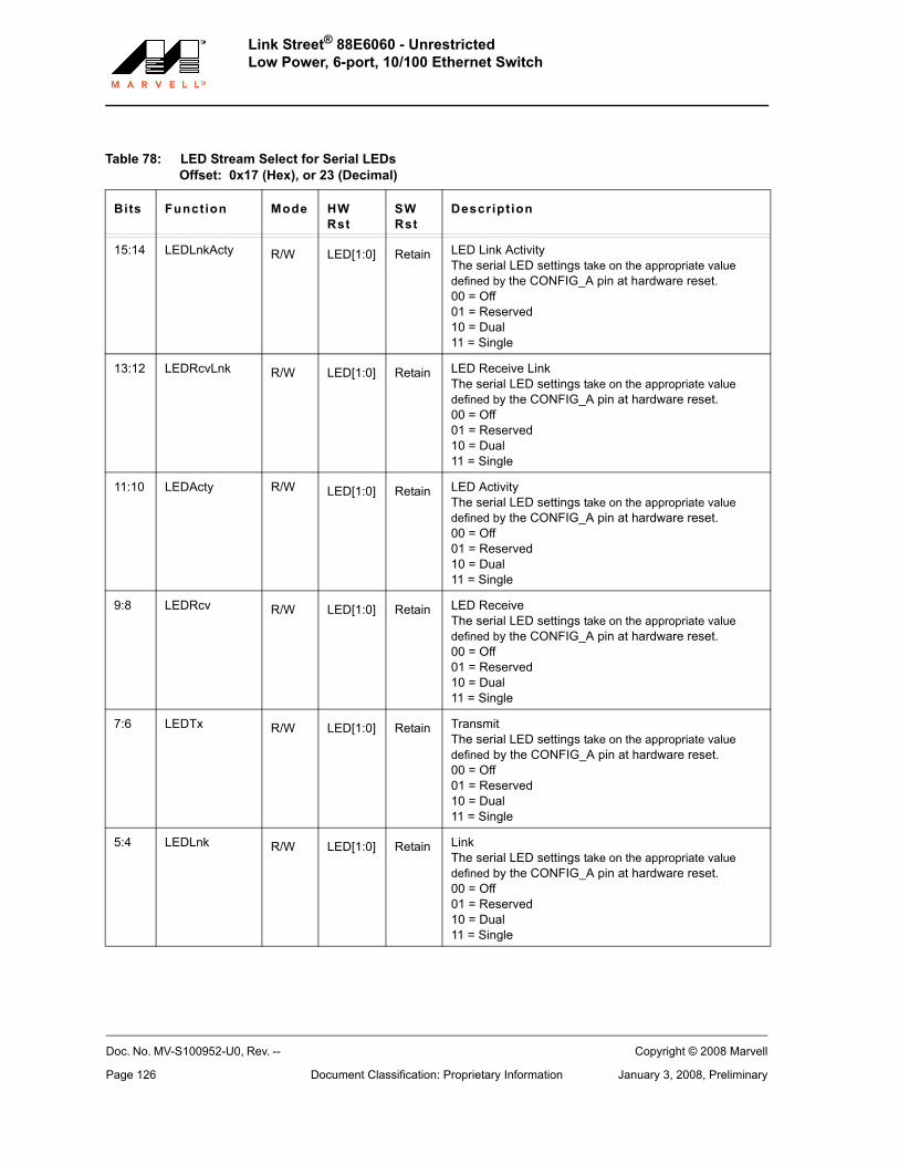
Link Street® 88E6060 - UnrestrictedLow Power, 6-port, 10/100 Ethernet Switch
Doc. No. MV-S100952-U0, Rev. -- Copyright © 2008 Marvell
Page 126 Document Classification: Proprietary Information January 3, 2008, Preliminary
Table 78: LED Stream Select for Serial LEDsOffset: 0x17 (Hex), or 23 (Decimal)
Bits Function Mode HWRst
SWRst
Description
15:14 LEDLnkActy R/W LED[1:0] Retain LED Link ActivityThe serial LED settings take on the appropriate value defined by the CONFIG_A pin at hardware reset. 00 = Off01 = Reserved10 = Dual11 = Single
13:12 LEDRcvLnk R/W LED[1:0] Retain LED Receive LinkThe serial LED settings take on the appropriate value defined by the CONFIG_A pin at hardware reset. 00 = Off01 = Reserved10 = Dual11 = Single
11:10 LEDActy R/W LED[1:0] Retain LED ActivityThe serial LED settings take on the appropriate value defined by the CONFIG_A pin at hardware reset.00 = Off01 = Reserved10 = Dual11 = Single
9:8 LEDRcv R/W LED[1:0] Retain LED ReceiveThe serial LED settings take on the appropriate value defined by the CONFIG_A pin at hardware reset.00 = Off01 = Reserved10 = Dual11 = Single
7:6 LEDTx R/W LED[1:0] Retain TransmitThe serial LED settings take on the appropriate value defined by the CONFIG_A pin at hardware reset.00 = Off01 = Reserved10 = Dual11 = Single
5:4 LEDLnk R/W LED[1:0] Retain LinkThe serial LED settings take on the appropriate value defined by the CONFIG_A pin at hardware reset.00 = Off01 = Reserved10 = Dual11 = Single

PHY Registers
Copyright © 2008 Marvell Doc. No. MV-S100952-U0, Rev. --
January 3, 2008, Preliminary Document Classification: Proprietary Information Page 127
3:2 LEDSpd R/W LED[1:0] Retain SpeedThe serial LED settings take on the appropriate value defined by the CONFIG_A pin at hardware reset.00 = Off01 = Reserved10 = Dual11 = Single
1:0 LEDDx/COLX
R/W LED[1:0] Retain LED Duplex/ COLXThe serial LED settings take on the appropriate value defined by the CONFIG_A pin at hardware reset.00 = Off01 = Reserved10 = Dual11 = Single
Table 78: LED Stream Select for Serial LEDs (Continued)Offset: 0x17 (Hex), or 23 (Decimal)
Bits Function Mode HWRst
SWRst
Description

Link Street® 88E6060 - UnrestrictedLow Power, 6-port, 10/100 Ethernet Switch
Doc. No. MV-S100952-U0, Rev. -- Copyright © 2008 Marvell
Page 128 Document Classification: Proprietary Information January 3, 2008, Preliminary
Table 79: PHY LED Control Register (Global1)Offset: 0X18 (Hex), 0r 24 (Decimal)
1. This global register is accessible for writing or reading from any PHY port (i.e., only one physical register exists for all the PHY Ports).
Bits Field Mode HWRst
SWRst
Description
15 Reserved RO Always 0 Always 0 Must be 0.
14:12 PulseStretch R/W 0x4 Retain Pulse stretch duration. Default Value = 100.000 = No pulse stretching001 = 21 ms to 42 ms010 = 42 ms to 84 ms011 = 84 ms to 170 ms100 = 170 ms to 340 ms101 = 340 ms to 670 ms110 = 670 ms to 1.3s111 = 1.3s to 2.7s
11:9 BlinkRate R/W 0x1 Retain Blink Rate. This is a global setting.Default Value = 001000 = 42 ms001 = 84 ms010 = 170 ms011 = 340 ms100 = 670 ms101 to 111 = Reserved
8:6 SrStrUpdate R/W 0x2 Retain Serial Stream Update000 = 10 ms001 = 21 ms010 = 42 ms011 = 84 ms100 = 170 ms101 = 340 ms110 to 111 = Reserved
5:4 Duplex R/W LED[1:0]00 = Off01 = Single10 = Single11 = Single
Retain 00 = Off01 = Reserved10 = Dual11 = Single
3:2 Error R/W 11 Retain 00 = Off01 = Reserved10 = Dual11 = Single
1:0 COLX R/W LED[1:0]00 = Off01 = Single10 = Single11 = Single
Retain 00 = Off01 = Reserved10 = Dual11 = Single

PHY Registers
Copyright © 2008 Marvell Doc. No. MV-S100952-U0, Rev. --
January 3, 2008, Preliminary Document Classification: Proprietary Information Page 129
Table 80: PHY Manual LED OverrideOffset: 0x19 (Hex), or 25 (Decimal)
Bits Field Mode HWRst
SWRst
Descript ion
15:6 Reserved R/W 0x0 Retain 0000000000
5:4 LED2 R/W 0x0 Retain 00 = Normal01 = Blink10 = LED Off11 = LED On
3:2 LED1 R/W 0x0 Retain 00 = Normal01 = Blink10 = LED Off11 = LED On
1:0 LED0 R/W 0x0 Retain 00 = Normal01 = Blink10 = LED Off11 = LED On

Link Street® 88E6060 - UnrestrictedLow Power, 6-port, 10/100 Ethernet Switch
Doc. No. MV-S100952-U0, Rev. -- Copyright © 2008 Marvell
Page 130 Document Classification: Proprietary Information January 3, 2008, Preliminary
Table 81: VCT™ Register for TXP/N PinsOffset: 0x1A1 (Hex), or 26 (Decimal)
1. The results stored in this register apply to the TX pin pair.
Bits Field Mode HWRst
SWRst
Description
15 EnVCT R/W, SC
0x0 0x0 Enable VCTThe 88E6060 device must be in forced 100 Mbps mode before enabling this bit.1 = Run VCT0 = VCT completedAfter running VCT once, bit 15 = 0 indicates VCT com-pleted. The cable status is reported in the VCTTst bits in regis-ters 26 and 27. Refer to the “Virtual Cable Tester™” feature in section 4.5.
14:13 VCTTst RO 0x0 Retain VCT Test StatusThese VCT test status bits are valid after completion of VCT.11 = Test fail00 = valid test, normal cable (no short or open in cable)10 = valid test, open in cable (Impedance > 333 ohm)01 = valid test, short in cable (Impedance < 33 ohm)
12:8 AmpRfln RO 0x0 Retain Amplitude of ReflectionThe amplitude of reflection is stored in these register bits. These amplitude bits range from 0x07 to 0x1F. 0x1F = Maximum positive amplitude0x13 = Zero amplitude0x07 = Maximum negative amplitudeThese bits are valid after completion of VCT (bit 15) and if the VCT test status bits (bits 14:13) have not indicated test failure.
7:0 DistRfln RO 0x0 Retain Distance of ReflectionThese bits refer to the approximate distance (±1m) to the open/short location, measured at nominal conditions (room temperature and typical VDDs). See Figure 26.These bits are valid after completion of VCT (bit 15) and if the VCT test status bits (bit 14:13) have not indicated test failure.

PHY Registers
Copyright © 2008 Marvell Doc. No. MV-S100952-U0, Rev. --
January 3, 2008, Preliminary Document Classification: Proprietary Information Page 131
Figure 26: Cable Fault Distance Trend Line
Table 82: VCT™ Register for RXP/N pinsOffset: 0x1B1 (Hex), or 27 (Decimal)
1. The results stored in this register apply to the RX pin pair.
Bits Field Mode HWRst
SWRst
Description
15 Reserved RO Always 0
Always 0
Reserved
14:13 VCTTst RO 0 Retain VCT Test StatusThe VCT test status bits are valid after completion of VCT.11 = Test fail00 = valid test, normal cable (no short or open in cable)10 = valid test, open in cable (Impedance > 333 ohm)01 = valid test, short in cable (Impedance < 33 ohm)
12:8 AmpRfln RO 0 Retain Amplitude of ReflectionThe amplitude of reflection is stored in these register bits. These amplitude bits range from 0x07 to 0x1F. 0x1F = Maximum positive amplitude0x13 = Zero amplitude0x07 = Maximum negative amplitudeThese bits are valid after completion of VCT (bit 15) and if VCT test status bits (bit 14:13) have not indicated test failure.
7:0 DistRfln RO 0 Retain Distance of ReflectionThese bits refer to the approximate distance (±1m) to the open/short location, measured at nominal conditions (room temperature and typical VDDs). See Figure 26.These bits are valid after completion of VCT (bit 15) and if VCT test status bits (bits 14:13) have not indicated test failure.
Register 27[7:0] or 26[7:0]
RX/TX
200150100500
0 50 100 150 150 200 250 300
y = 0.7816x - 18.261

Link Street® 88E6060 - UnrestrictedLow Power, 6-port, 10/100 Ethernet Switch
Doc. No. MV-S100952-U0, Rev. -- Copyright © 2008 Marvell
Page 132 Document Classification: Proprietary Information January 3, 2008, Preliminary
Note
Registers 0x1D through 0x1F (hexadecimal (29 through 31 decimal) are reserved. Do not read or write to these registers.
Table 83: PHY Specific Control Register IIOffset: 0x1C (Hex), or 28 (Decimal)
Bits Field Mode HWRst
SWRst
Descript ion
15:1 Reserved R/W 0x0 0x0 Must be 000000000000000
0 SelClsA R/W SEL_CLASSA
Update 1 = Select Class A driver; available for 100BASE-TX mode only —typically used in backplane or direct connect applications
0 = Select Class B driver—typically used in CAT 5 applications

EEPROM Programming FormatEEPROM Programming Details
Copyright © 2008 Marvell Doc. No. MV-S100952-U0, Rev. --
January 3, 2008, Preliminary Document Classification: Proprietary Information Page 133
Section 8. EEPROM Programming Format
8.1 EEPROM Programming DetailsThe 88E6060 device supports an optional external serial EEPROM device for programing its internal registers. The EEPROM data is read in once after RESETn is deasserted if the stand alone Switch Mode is not selected (see Table 14 on page 29).
The 88E6060 supports 1K bit (93C46), 2K bit (93C56), or 4K bit (93C66) EEPROM devices. The size of the device is selected by the EE_DIN/EE_1K pin at reset—see Table 7 on page 21. The external EEPROM device must be configured in x16 data organization mode.
Regardless of which particular device is attached, the EEPROM is read and processed in the same way:
1. Start at EEPROM address 0x00.2. Read in the 16 bits of data from the even address. This step is called the Command.3. If the just read in Command is all ones, terminate the serial EEPROM reading process and go to step 8.4. Increment the address by 1—to the next address.5. Read in the 16 bits of data from that address—This is called the RegData.6. Write RegData to the locations defined by the previous Command.7. Go to step 2.8. Set the EEInt bit in Global Status to a one (Table 49, on page 99) generating an Interrupt (if enabled).9. Done.
The 16-bit Command determines which register or registers inside the 88E6060 are updated as follows. Refer to Figure 27 below.
• Bit 15 determines which set of registers can be written.If bit 15 = 0 the PHY registers can be written (SMI Device Addresses 0x00 to 0x04) or the Switch Global reg-isters can be written (SMI Device Address 0x7). If bit 15 = 1 the Switch registers can be written (SMI Device Addresses 0x08 to 0x0D). See section 6 and Figure 25 for more information on the registers and their addresses.
• Bits 10:5 (or 9:5), the Device Vector, determines which Device Addresses are written. Each bit of the Device Vector that is set to a one causes one Device Address to be written. Bit 5 controls writes for Port 0 (either PHY address 0x00 or Switch address 0x08).
• Bit 6 controls writes for Port 1 (either PHY address 0x01 or Switch address 0x09).• Bit 7 controls writes for Port 2, etc.• The Switch Global registers (Switch address 0x0F) are written when bit 15 is a zero and bits 14:5 are ones.
Care is needed to ensure that Reserved registers are not written.• Bits 4:0, the Register Address, determine which SMI Register Address is written.

Link Street® 88E6060 - UnrestrictedLow Power, 6-port, 10/100 Ethernet Switch
Doc. No. MV-S100952-U0, Rev. -- Copyright © 2008 Marvell
Page 134 Document Classification: Proprietary Information January 3, 2008, Preliminary
The format of the EEPROM Commands supports writing the same RegData to all the PHYs or all the Switch’s MACs with one Command/RegData pair. The Command/RegData list can be as short or as long as needed. This makes optimum use of the limited number of Command/RegData pairs that can fit in a given size EEPROM1. The maximum number of Command/RegData pairs is one fewer than might be expected from a simple calculation because the last entry must be the End of List or Halt Indicator of all ones.
Figure 27: EEPROM Data Format
1. 31 in the 93C46, 63 in the 93C56, and 127 in the 93C66 EEPROM.
Register Address
15 14 5 4 0
Addr 0
Any Even Addr
Any Odd Addr
Register Data Written to Switch Register(s)
Device Vector1
Register Address
Register Data Written to PHY Register(s)
Device Vector0
Register Address
Register Data Written to a Switch Global Register
0
Last Used Even Addr End of List Indicator = all 1's at 1st Even Addr
Addr 1
Addr 2
Addr 3
Switch Command
PHY Command
Global Command
Command
RegData
RegData
RegData
78
1 1 1 1 1 1 1 1 1 1
6
15 14 5 4 078 6
0 0 0 0 0
000
91011
0

Electrical SpecificationsAbsolute Maximum Ratings
Copyright © 2008 Marvell Doc. No. MV-S100952-U0, Rev. --
January 3, 2008, Preliminary Document Classification: Proprietary Information Page 135
Section 9. Electrical Specifications
9.1 Absolute Maximum RatingsStresses above those listed in Absolute Maximum Ratings may cause permanent device failure. Functionality at or above these limits is not implied. Exposure to absolute maximum ratings for extended periods may affect device reliability.
Table 84: Absolute Maximum Ratings
Symbol Parameter Min Typ Max Units
VDD(3.3) Power Supply Voltage on VDDO with respect to VSS
-0.5 3.3 +3.6 V
VDD(2.5) Power Supply Voltage on VDDAH with respect to VSS
-0.5 2.5 +3.6 orVDD(3.3)+0.51
whichever is less
1. VDD(2.5) must never be more than 0.5V greater than VDD(3.3) or damage will result. This implies that power must be applied to VDD(3.3) before or at the same time as VDD(2.5).
V
VDD(1.5) Power Supply Voltage on VDD, or VDDAL with respect to VSS
-0.5 1.5 +3.6 orVDD(2.5)+0.52
whichever is less
2. VDD(1.5) must never be more than 0.5V greater than VDD(2.5) or damage will result. This implies that power must be applied to VDD(2.5) before or at the same time as VDD(1.5).
V
VPIN Voltage applied to any input pin with respect to VSS
-0.5 +3.6 or VDDO+0.53
whichever is less
3. VPIN must never be more than 0.5V greater than VDDO or damage will result.
V
TSTORAGE Storage temperature -55 +1254
4. 125°C is the re-bake temperature. For extended storage time greater than 24 hours, +85°C should be the maximum.
°C

Link Street® 88E6060 - UnrestrictedLow Power, 6-port, 10/100 Ethernet Switch
Doc. No. MV-S100952-U0, Rev. -- Copyright © 2008 Marvell
Page 136 Document Classification: Proprietary Information January 3, 2008, Preliminary
9.2 Recommended Operating Conditions
Table 85: Recommended Operating Conditions
Symbol Parameter Condition Min Typ Max Units
VDD(3.3) 3.3V power supply For pins VDDO 3.135 3.3 3.465 V
VDD(2.5) 2.5V power supply For pins VDDAH 2.375 2.5 2.625 V
VDD(1.5) 1.5V power supply For pinsVDD, VDDAL
1.425 1.5 1.575 V
TA Ambient operating temperature
Commercial Parts 0 70 °C
Industrial Parts1
1. Industrial part numbers have an “I” following the commercial part numbers. See “Ordering Information” on page 162.
-40 85 °C
TJ Maximum junction temperature
1252
2. Refer to white paper on TJ Thermal Calculations for more Information.
°C
RSET Internal bias reference Resistor value placed between RSET- and RSET+ pins
1980 2000 2020 Ω
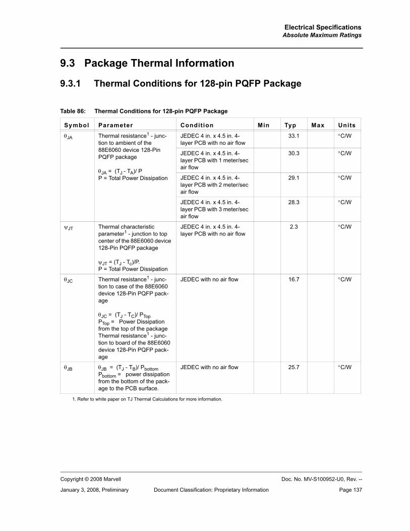
Electrical SpecificationsAbsolute Maximum Ratings
Copyright © 2008 Marvell Doc. No. MV-S100952-U0, Rev. --
January 3, 2008, Preliminary Document Classification: Proprietary Information Page 137
9.3 Package Thermal Information
9.3.1 Thermal Conditions for 128-pin PQFP Package
Table 86: Thermal Conditions for 128-pin PQFP Package
Symbol Parameter Condition Min Typ Max Units
θJA Thermal resistance1 - junc-tion to ambient of the 88E6060 device 128-Pin PQFP package
θJA = (TJ - TA)/ PP = Total Power Dissipation
1. Refer to white paper on TJ Thermal Calculations for more information.
JEDEC 4 in. x 4.5 in. 4-layer PCB with no air flow
33.1 °C/W
JEDEC 4 in. x 4.5 in. 4-layer PCB with 1 meter/sec air flow
30.3 °C/W
JEDEC 4 in. x 4.5 in. 4-layer PCB with 2 meter/sec air flow
29.1 °C/W
JEDEC 4 in. x 4.5 in. 4-layer PCB with 3 meter/sec air flow
28.3 °C/W
ψJT Thermal characteristic parameter1 - junction to top center of the 88E6060 device 128-Pin PQFP package
ψJT = (TJ - Tc)/P.P = Total Power Dissipation
JEDEC 4 in. x 4.5 in. 4-layer PCB with no air flow
2.3 °C/W
θJC Thermal resistance1 - junc-tion to case of the 88E6060 device 128-Pin PQFP pack-age
θJC = (TJ - TC)/ PTopPTop = Power Dissipation from the top of the package Thermal resistance1 - junc-tion to board of the 88E6060 device 128-Pin PQFP pack-age
JEDEC with no air flow 16.7 °C/W
θJB θJB = (TJ - TB)/ PbottomPbottom = power dissipation from the bottom of the pack-age to the PCB surface.
JEDEC with no air flow 25.7 °C/W

Link Street® 88E6060 - UnrestrictedLow Power, 6-port, 10/100 Ethernet Switch
Doc. No. MV-S100952-U0, Rev. -- Copyright © 2008 Marvell
Page 138 Document Classification: Proprietary Information January 3, 2008, Preliminary
9.4 DC Electrical Characteristics(Over full range of values listed in the Recommended Operating Conditions unless otherwise specified)
Table 87: DC Electrical Characteristics
Symbol Parameter Pins Condition Min Typ1
1. The values listed are typical values with LED mode 3, 3 LEDs per port, and Auto-Negotiation on.
Max UnitsIDD(3.3) 3.3 volt
Power to outputs
VDDO No link on any port 15 mA
All ports 10 Mbps 17 mA
All ports 100 Mbps 22 mA
Power Down Mode 18 mA
Sleep Mode 18 mA
IDD(2.5) 2.5 volt2 Power to analog core
2. The 2.5V power source must supply an additional 100 mA (Typical) current from the center tap on the magnetics. (This number is not included in this table.)
VDDAH No link on any port 40 mA
All ports 10 Mbps and active
126 mA
All ports 100 Mbps 111 mA
Power Down Mode 32 mA
Sleep Mode 36 mA
2.5 volt3 Power toCenter Tap
3. The 2.5V power source must supply an additional 100 mA (Typical) current from the center tap on the magnetics. (This number is not included in this table.)
External Magnetics Center Tap Pin
No link on any port 10 mA
All ports 10 Mbps and active
301 mA
All ports 100 Mbps 103 mA
Power Down Mode 0 mA
Sleep Mode 0 mA
IDD(1.5) 1.5 volt Power to analog core
VDDAL No link on any port 0 mA
All ports 10 Mbps and active
1 mA
All ports 100 Mbps 29 mA
Power Down Mode 1 mA
Sleep Mode 0 mA
1.5 volt Power to digital core
VDD No link on any port 40 mA
All ports 10 Mbps and active
54 mA
All ports 100 Mbps and active
119 mA
Power Down Mode 39 mA
Sleep Mode 36 mA

Electrical SpecificationsAbsolute Maximum Ratings
Copyright © 2008 Marvell Doc. No. MV-S100952-U0, Rev. --
January 3, 2008, Preliminary Document Classification: Proprietary Information Page 139
9.4.1 Digital Operating Conditions(Over full range of values listed in the Recommended Operating Conditions unless otherwise specified)
Table 88: Digital Operating Conditions
Symbol Parameter Pins Condition Min Typ Max Units
VIH High level input voltage
All pins 2.0 VDDO+0.5
V
XTAL_IN 1.4 V
VIL Low level input voltage
All pins -0.5 0.8 V
XTAL_IN 0.6 V
VOH High level output voltage
LED pins1
1. The LED pins are as follows: P4_LED2[2:0], P3_LED1[2:0], P2_LED2[2:0], P1_LED1[2:0], P0_LED1[2:0]
IOH = -8 mAVDDO = Min
2.4 V
XTAL_OUT IOH = -1 mA VIH(XTAL_IN)+0.2
V
All others IOH = -4 mAVDDO = Min
2.4 V
VOL Low level output voltage
LED pins1 IOL= 8 mA 0.4 V
XTAL_OUT IOL = 1 mA VIL(XTAL_IN)-0.2
V
INTn pin2 IOL= 8 mA V
All others IOL= 4 mA 0.4 V
IILK Input leakage current
With pull-up resistor (typ. 120 kΩ)
0<VIN<VDDO + 10- 50
μA
With pull-downresistor (typ. 120 kΩ)
0<VIN<VDDO + 50- 10
μA
All others 0<VIN<VDDO ±10 μA
CIN Input capacitance
All pins 5 pF

Link Street® 88E6060 - UnrestrictedLow Power, 6-port, 10/100 Ethernet Switch
Doc. No. MV-S100952-U0, Rev. -- Copyright © 2008 Marvell
Page 140 Document Classification: Proprietary Information January 3, 2008, Preliminary
Table 89: Internal Resistor Description
Pin # Pin Name Resistor Pin # Pin Name Resistor
34, 33 SW_MODE[1:0] Internal pull-up 82 P5_INCLK Internal pull-up
36 LEDSER Internal pull-up 83, 84, 85, 86 P5_IND[3:0] Internal pull-up
37 LEDCLK Internal pull-up 87 P5_INDV Internal pull-down
38 LEDENA Internal pull-up 89 DISABLE_MII4 Internal pull-up
58 EE_DOUT Internal pull-up 91 P4_CRS Internal pull-down
60 EE_CLK/ADDR4
Internal pull-up 93 CONFIG_B Internal pull-up
61 EE_CS/EE_1K
Internal pull-up 94 P4_COL Internal pull-down
64 FD_FLOW_DIS Internal pull-up 95, 96, 97, 98 P4_OUTD[3:0]/P4_MODE[3:0]
Internal pull-up
66 ENABLE_MII5 Internal pull-up 99 P4_OUTCLK Internal pull-up
68 CLK_SEL Internal pull-up 102 P4_INCLK Internal pull-up
69 EE_DIN/HD_FLOW_DIS
Internal pull-up 106 CONFIG_A Internal pull-up
70 MDC Internal pull-up 108 P1_CONFIG Internal pull-down
71 MDIO Internal pull-up 110 RESETn None
72 P5_CRS Internal pull-down 111 P0_CONFIG Internal pull-down
73 P5_COL Internal pull-down 112, 114, 116, 117
P4_IND[3:0] Internal pull-up
74, 75, 76, 77 P5_OUTD[3:0]/P5_MODE[3:0]
Internal pull-up 118 P4_INDV Internal pull-down
79 P5_OUTCLK Internal pull-up 122 P0_SDET None
81 P5_OUTDV/WD_DIS
Internal pull-up 127 P1_SDET None

Electrical SpecificationsAbsolute Maximum Ratings
Copyright © 2008 Marvell Doc. No. MV-S100952-U0, Rev. --
January 3, 2008, Preliminary Document Classification: Proprietary Information Page 141
9.4.2 IEEE DC Transceiver ParametersIEEE tests are typically based on templates and cannot simply be specified by a number. For an exact description of the template and the test conditions, refer to the IEEE specifications:-10BASE-T IEEE 802.3 Clause 14-100BASE-TX ANSI X3.263-1995(Over full range of values listed in the Recommended Operating Conditions unless otherwise specified)
Table 90: IEEE DC Transceiver Parameters
Symbol Parameter Pins Condition Min Typ Max Units
VODIFF Absolute peak differential output voltage
TXP/N[1:0] 10BASE-T no cable 2.2 2.5 2.8 V
TXP/N[1:0] 10BASE-T cable model 5851
1. IEEE 802.3 Clause 14, Figure 14.9 shows the template for the “far end” wave form. This template allows as little as 495 mV peak dif-ferential voltage at the far end receiver.
mV
TXP/N[0] 100BASE-FX mode 0.4 0.8 1.2 V
TXP/N[1:0] 100BASE-TX mode 0.950 1.0 1.05 V
Overshoot2
2. ANSI X3.263-1995 Figure 9-1.
TXP/N[4:0] 100BASE-TX mode 0 5% V
Amplitude Symmetry(positive/negative)
TXP/N[1:0] 100BASE-TX mode 0.98x 1.02x V+/V-
VIDIFF Peak Differential Input Voltage accept level
RXP/N[1:0] 10BASE-T mode 5853
3. The input test is actually a template test. IEEE 802.3 Clause 14, Figure 14.17 shows the template for the receive wave form.
mV
RXP/N[0]P[1:0]_SDETP/N
100BASE-FX mode 200 mV
Signal Detect Assertion
RXP/N[1:0] 100BASE-TX mode 1000 4604
4. The ANSI TP-PMD specification requires that any received signal with peak-to-peak differential amplitude greater than 1000 mV should turn on signal detect (internal signal in 100BASE-TX mode). The 88E6060 will accept signals typically with 460 mV peak-to-peak differential amplitude.
mVpeak-peak
Signal Detect De-assertion
RXP/N[1:0] 100BASE-TX mode 200 3605
5. The ANSI TP-PMD specification requires that any received signal with peak-to-peak differential amplitude less than 200 mV should be de-assert signal detect (internal signal in 100BASE-TX mode). The 88E6060 will reject signals typically with peak-to-peak differ-ential amplitude less than 360 mV.
mVpeak-peak

Link Street® 88E6060 - UnrestrictedLow Power, 6-port, 10/100 Ethernet Switch
Doc. No. MV-S100952-U0, Rev. -- Copyright © 2008 Marvell
Page 142 Document Classification: Proprietary Information January 3, 2008, Preliminary
9.5 AC Electrical Specifications9.5.1 Reset and Configuration Timing(Over full range of values listed in the Recommended Operating Conditions unless otherwise specified.)
Table 91: Reset and Configuration Timing
Symbol Parameter Condition Min Typ Max Units Notes
TPU_RESET
Valid power to RESETn de-asserted or RESETn assertion time
At power up or subse-quent resets after power up
10 ms
TSU_CLK
Number of valid XTAL_IN cycles prior to RESETn de-asserted
10 Cycles
TSU
Configuration data valid prior to RESETn de-asserted
200 ns 1
1. When RESETn is low all configuration pins become inputs, and the value seen on these pins is latched on the rising edge of RESETn.
THD
Configuration data valid after RESETn de-asserted 0 ns
TCO
Configuration output driven after RESETn de-asserted
40 ns 2
2. P[x]_OUTD[3:0]/P[x]_MODE[3:0] are normally outputs that are also used to configure the 88E6060 device during hardware reset. When reset is asserted, these pins become inputs and the required LED configuration is latched at the rising edge of RESETn.

Electrical SpecificationsAbsolute Maximum Ratings
Copyright © 2008 Marvell Doc. No. MV-S100952-U0, Rev. --
January 3, 2008, Preliminary Document Classification: Proprietary Information Page 143
Figure 28: Reset and Configuration Timing
Power
CLK
RESETn
Config Data
TPU_RESET
TSU_CLK
TSU THD
Config Pins Output
TCO

Link Street® 88E6060 - UnrestrictedLow Power, 6-port, 10/100 Ethernet Switch
Doc. No. MV-S100952-U0, Rev. -- Copyright © 2008 Marvell
Page 144 Document Classification: Proprietary Information January 3, 2008, Preliminary
9.5.2 Clock Timing when using a 25 MHz Oscillator(Over full range of values listed in the Recommended Operating Conditions unless otherwise specified.)
Figure 29: Oscillator Clock Timing
Table 92: Clock Timing with a 25 MHz Oscillator
Symbol Parameter Condition Min Typ Max Units Notes
TP XTAL_IN period40
-50 ppm40 40
+50 ppmns 25 MHz
TH XTAL_IN high time 16 ns
TL XTAL_IN low time 16 ns
TR XTAL_IN rise 3 ns
TF XTAL_IN fall 3 ns
TP
TH TL
TR
2.0 V
0.8V
TF
XTAL_IN

Electrical SpecificationsAbsolute Maximum Ratings
Copyright © 2008 Marvell Doc. No. MV-S100952-U0, Rev. --
January 3, 2008, Preliminary Document Classification: Proprietary Information Page 145
9.5.3 MII Receive Timing—PHY ModeIn PHY mode, the P[x]_INCLK pins are outputs.(Over full range of values listed in the Recommended Operating Conditions unless otherwise specified)
Figure 30: PHY Mode MII Receive Timing
Table 93: MII Receive Timing—PHY Mode
Symbol Parameter Condition Min Typ Max Units Notes
TP_TX_CLK P[x]_INCLK period10BASE mode 400 ns 1
1. 2.5 MHz for 10 Mbps or 25 MHz for 100 Mbps.
100BASE mode
40 ns 1
TH_TX_CLK P[x]_INCLK high10BASE mode 160 200 240 ns
100BASE mode
16 20 24 ns
TL_TX_CLK P[x]_INCLK low10BASE mode 160 200 240 ns
100BASE mode
16 20 24 ns
TSU_TX
MII inputs (P[x]_IND[3:0], P[x]_INDV) valid prior to P[x]_INCLK going high.
15 ns
THD_TX
MII inputs (P[x]_IND[3:0], P[x]_INDV) valid after P[x]_INCLK going high.
0 ns
INCLK
INPUTS
THD_TX
TP_TX_CLK
TSU_TX
TH_TX_CLK
TL_TX_CLK
INCLK is the clock used to clock the input data.It is an output in this mode.
NOTE:

Link Street® 88E6060 - UnrestrictedLow Power, 6-port, 10/100 Ethernet Switch
Doc. No. MV-S100952-U0, Rev. -- Copyright © 2008 Marvell
Page 146 Document Classification: Proprietary Information January 3, 2008, Preliminary
9.5.4 MII Transmit Timing—PHY ModeIn PHY mode, the P[x]_OUTCLK pins are outputs.(Over full range of values listed in the Recommended Operating Conditions unless otherwise specified)
Figure 31: PHY Mode MII Transmit Timing
Table 94: MII Transmit Timing—PHY Mode
Symbol Parameter Condition Min Typ Max Units Notes
TP_RX_CLK P[x]_OUTCLK period10BASE mode 400 ns 1
1. 2.5 MHz for 10 Mbps or 25 MHz for 100 Mbps.
100BASE mode 40 ns 1
TH_RX_CLK P[x]_OUTCLK high10BASE mode 160 200 240 ns
100BASE mode 16 20 24 ns
TL_RX_CLK P[x]_OUTCLK low10BASE mode 160 200 240 ns
100BASE mode 16 20 24 ns
TCQ_MAX
P[x]_OUTCLK to outputs(P[x]_OUTD[3:0],P[x]_OUTDV) valid
25 ns
TCQ_MIN
P[x]_OUTCLK to outputsP[x]_OUTD[3:0],P[x]_OUTDV) invalid
10 ns
OUTCLK
OUTPUTS
TP_RX_CLK
TCQ_MAX TCQ_MIN
TH_RX_CLK
TL_RX_CLK
OUTCLK is the clock used to clock the output data.It is an output in this mode.
NOTE:

Electrical SpecificationsAbsolute Maximum Ratings
Copyright © 2008 Marvell Doc. No. MV-S100952-U0, Rev. --
January 3, 2008, Preliminary Document Classification: Proprietary Information Page 147
9.5.5 MAC Mode Clock TimingIn MAC mode, INCLK and OUTCLK are inputs. (Over full range of values listed in the Recommended Operating Conditions unless otherwise specified)
Figure 32: MAC Clock Timing
Table 95: MAC Mode Clock Timing
Symbol Parameter Condition Min Typ Max Units Notes
TP MACCLK_IN period0 4
or 40
40+50 ppm
ns DC to 25 MHz
TH MACCLK_IN high time 16 ns
TL MACCLK_IN low time 16 ns
TR MACCLK_IN rise 3 ns
TF MACCLK_IN fall 3 ns
TP
TH TL
TR
2.0 V
0.8V
TF
MACCLK

Link Street® 88E6060 - UnrestrictedLow Power, 6-port, 10/100 Ethernet Switch
Doc. No. MV-S100952-U0, Rev. -- Copyright © 2008 Marvell
Page 148 Document Classification: Proprietary Information January 3, 2008, Preliminary
9.5.6 MII Receive Timing—MAC ModeIn MAC mode, the P[x]_INCLK pins are inputs.(Over full range of values listed in the Recommended Operating Conditions unless otherwise specified)
Figure 33: MAC Mode MII Receive Timing
Table 96: MII Receive Timing—MAC Mode
Symbol Parameter Condition Min Typ Max Units Notes
TSU_RX
MII inputs (P[x]_IND[3:0], P[x]_INDV) valid prior to P[x]_INCLK going high
With 10 pF load
10 ns
THD_RX
MII inputs (P[x]_IND[3:0], P[x]_INDV) valid after P[x]_INCLK going high
With 10 pF load
10 ns
INCLK
INPUTS
THD_RX
TSU_RX
INCLK is the clock used to clock the input data.It is an input in this mode.
NOTE:

Electrical SpecificationsAbsolute Maximum Ratings
Copyright © 2008 Marvell Doc. No. MV-S100952-U0, Rev. --
January 3, 2008, Preliminary Document Classification: Proprietary Information Page 149
9.5.7 MII Transmit Timing—MAC ModeIn MAC mode, the P[x]_OUTCLK pins are inputs.(Over full range of values listed in the Recommended Operating Conditions unless otherwise specified)
Figure 34: MAC Mode MII Transmit Timing
Table 97: MII Transmit Timing—MAC Mode
Symbol Parameter Condition Min Typ Max Units Notes
TCQ_MAX
P[x]_OUTCLK to outputs(P[x]_OUTD[3:0],P[x]_OUTDV) valid
With 10 pF load
25 ns
TCQ_MIN
P[x]_OUTCLK to outputs(P[x]_OUTD[3:0],P[x]_OUTDV) invalid
With 10 pF load
0 ns
OUTCLK
OUTPUTS
TCQ_MAX TCQ_MIN
OUTCLK is the clock used to clock the output data.It is an input in this mode.
NOTE:

Link Street® 88E6060 - UnrestrictedLow Power, 6-port, 10/100 Ethernet Switch
Doc. No. MV-S100952-U0, Rev. -- Copyright © 2008 Marvell
Page 150 Document Classification: Proprietary Information January 3, 2008, Preliminary
9.5.8 SNI Falling Edge Receive Timing(Over full range of values listed in the Recommended Operating Conditions unless otherwise specified)
Figure 35: SNI Falling Edge Receive Timing
Table 98: SNI Falling Edge Receive Timing
Symbol Parameter Condit ion Min Typ Max Units Notes
TP_FRX_CLK SNI falling edge INCLK period
10BASE-T Mode
100 ns
TH_FRX_CLK SNI falling edge INCLK high
35 50 65 ns
TL_FRX_CLK SNI falling edge INCLK low
35 50 65 ns
TSU_FRX SNI receive data valid prior to INCLK going low
20 ns
THD_FRX SNI receive data valid after INCLK going low
10 ns
INCLK
INPUTS
THD_FRX
TP_FRX_CLK
TSU_FRX
TH_FRX_CLK
TL_FRX_CLK
INCLK is the clock used to clock the input data.It is an output in this mode.
NOTE:

Electrical SpecificationsAbsolute Maximum Ratings
Copyright © 2008 Marvell Doc. No. MV-S100952-U0, Rev. --
January 3, 2008, Preliminary Document Classification: Proprietary Information Page 151
9.5.9 SNI Falling Edge Transmit Timing(Over full range of values listed in the Recommended Operating Conditions unless otherwise specified)
Figure 36: SNI Falling Edge Transmit Timing
Table 99: SNI Falling Edge Transmit Timing
Symbol Parameter Condition Min Typ Max Units Notes
TP_FTX_CLK SNI falling edge OUTCLK period
10BASE-T Mode
100 ns
TH_FTX_CLK SNI falling edge OUTCLK high
35 50 65 ns
TL_FTX_CLKSNI falling edge OUTCLK low
35 50 65 ns
TCQ_MXFTX SNI falling edge OUTCLK to output valid
65 ns
TCQ_MNFTX SNI falling edge OUTCLK to output invalid
35 ns
OUTCLK
OUTPUTS
TP_FTX_CLK
TCQ_MNFTX
TL_FTX_CLK
TH_FTX_CLK
TCQ_MXFTX
OUTCLK is the clock used to clock the output data.It is an output in this mode.
NOTE:

Link Street® 88E6060 - UnrestrictedLow Power, 6-port, 10/100 Ethernet Switch
Doc. No. MV-S100952-U0, Rev. -- Copyright © 2008 Marvell
Page 152 Document Classification: Proprietary Information January 3, 2008, Preliminary
9.5.10 SNI Rising Edge Receive Timing(Over full range of values listed in the Recommended Operating Conditions unless otherwise specified)
Figure 37: SNI Rising Edge Receive Timing
Table 100: SNI Rising Edge Receive Timing
Symbol Parameter Condit ion Min Typ Max Units Notes
TP_RRX_CLK SNI rising edge INCLK period
10BASE-T Mode
100 ns
TH_RRX_CLK SNI rising edge INCLK high
35 50 65 ns
TL_RRX_CLK SNI rising edge INCLK low
35 50 65 ns
TSU_RRX SNI receive data valid prior to INCLK going high
20 ns
THD_RRX SNI receive data valid after INCLK going high
10 ns
INCLK
INPUTS
THD_RRX
TP_RRX_CLK
TSU_RRX
TH_RRX_CLK
TL_RRX_CLK
INCLK is the clock used to clock the input data.It is an output in this mode.
NOTE:

Electrical SpecificationsAbsolute Maximum Ratings
Copyright © 2008 Marvell Doc. No. MV-S100952-U0, Rev. --
January 3, 2008, Preliminary Document Classification: Proprietary Information Page 153
9.5.11 SNI Rising Edge Transmit Timing(Over full range of values listed in the Recommended Operating Conditions unless otherwise specified)
Figure 38: SNI Rising Edge Transmit Timing
Table 101: SNI Rising Edge Transmit Timing
Symbol Parameter Condition Min Typ Max Units Notes
TP_RTX_CLK SNI rising edge OUTCLK period
10BASE-T Mode
100 ns
TH_RTX_CLK SNI rising edge OUTCLK high
35 50 65 ns
TL_RTX_CLK SNI rising edge OUTCLK low
35 50 65 ns
TCQ_MXRTX OUTCLK to output valid 65 ns
TCQ_MNRTX OUTCLK to output invalid 35 ns
OUTCLK
OUTPUTS
TP_RTX_CLK
TCQ_MNRTX
TL_RTX_CLK
TH_RTX_CLK
TCQ_MXRTX
OUTCLK is the clock used to clock the output data.It is an output in this mode.
NOTE:

Link Street® 88E6060 - UnrestrictedLow Power, 6-port, 10/100 Ethernet Switch
Doc. No. MV-S100952-U0, Rev. -- Copyright © 2008 Marvell
Page 154 Document Classification: Proprietary Information January 3, 2008, Preliminary
9.5.12 RMII Receive Timing using INCLK(Over full range of values listed in the Recommended Operating Conditions unless otherwise specified)
Figure 39: PHY Mode RMII Receive Timing using INCLK
Table 102: RMII Receive Timing using INCLK
Symbol Parameter Condit ion Min Typ Max Units Notes
TP_TX_CLK P[x]_INCLK period 100BASE mode
20 ns 1
1. 50 MHz for 100 Mbps.
TH_TX_CLK P[x]_INCLK high 100BASE mode
8 10 12 ns
TL_TX_CLK P[x]_INCLK low 100BASE mode
8 10 12 ns
TSU_TX
MII inputs (P[x]_IND[1:0], P[x]_INDV) valid prior to P[x]_INCLK going high.
9.5 ns
THD_TX
MII inputs (P[x]_IND[1:0], P[x]_INDV) valid after P[x]_INCLK going high.
0ns
INCLK
INPUTS
THD_TX
TP_TX_CLK
TSU_TX
TH_TX_CLK
TL_TX_CLK
INCLK is the clock used to clock the input data.It is an output in this mode.
NOTE:

Electrical SpecificationsAbsolute Maximum Ratings
Copyright © 2008 Marvell Doc. No. MV-S100952-U0, Rev. --
January 3, 2008, Preliminary Document Classification: Proprietary Information Page 155
9.5.13 RMII Transmit Timing using INCLK(Over full range of values listed in the Recommended Operating Conditions unless otherwise specified)
Figure 40: PHY Mode RMII Transmit Timing using INCLK
Table 103: RMII Transmit Timing using INCLK
Symbol Parameter Condit ion Min Typ Max Units NotesTP_RX_CLK P[x]_INCLK period 100BASE mode 20 ns 1
1. 50 MHz for 100 Mbps.
TH_RX_CLK P[x]_INCLK high 100BASE mode 8 10 12 ns
TL_RX_CLK P[x]_INCLK low 100BASE mode 8 10 12 ns
TCQ_MAX
P[x]_INCLK to outputs(P[x]_OUTD[1:0],P[x]_OUTDV) valid
8.0 ns
TCQ_MIN
P[x]_INCLK to outputsP[x]_OUTD[1:0],P[x]_OUTDV) invalid
0 ns
INCLK
OUTPUTS
TP_RX_CLK
TCQ_MAX TCQ_MIN
TH_RX_CLK
TL_RX_CLK
INCLK is the clock used to clock the output data.It is an output in this mode.
NOTE:

Link Street® 88E6060 - UnrestrictedLow Power, 6-port, 10/100 Ethernet Switch
Doc. No. MV-S100952-U0, Rev. -- Copyright © 2008 Marvell
Page 156 Document Classification: Proprietary Information January 3, 2008, Preliminary
9.5.14 Serial LED Timing(Over full range of values listed in the Recommended Operating Conditions unless otherwise specified)
Figure 41: Serial LED Timing
Table 104: Serial LED Timing
Symbol Parameter Condit ion Min Typ Max Units Notes
TP_LEDCLK LEDCLK period 80 ns
TH_LEDCLK LEDCLK high 32 40 48 ns
TL_LEDCLK LEDCLK low 32 40 48 ns
TCQ_MAX LEDCLK falling edge to link outputs (LEDSER, LEDENA) valid
With 10 pF load
20 ns
TCQ_MIN LEDCLK falling edge to link outputs (LEDSER, LEDENA) invalid
With 10 pF load
0 ns
LEDCLK
OUTPUTS
TP_LEDCLK
TCQ_MIN
TL_LEDCLK
TH_LEDCLK
TCQ_MAX

Electrical SpecificationsAbsolute Maximum Ratings
Copyright © 2008 Marvell Doc. No. MV-S100952-U0, Rev. --
January 3, 2008, Preliminary Document Classification: Proprietary Information Page 157
9.5.15 Serial Management Interface Clock Timing(Over full range of values listed in the Recommended Operating Conditions unless otherwise specified)
Figure 42: Serial Management Interface Clock Timing
Table 105: Serial Management Interface Clock Timing
Symbol Parameter Condition Min Typ Max Units Notes
TP MDCCLK_IN period 120 ns 8.33 MHz
TH MDCCLK_IN high time 48 ns
TLMDCCLK_IN low time
48 ns
TR MDCCLK_IN rise 6 ns
TF MDCCLK_IN fall 6 ns
TP
TH TL
TR
2.0 V
0.8V
TF
MDC

Link Street® 88E6060 - UnrestrictedLow Power, 6-port, 10/100 Ethernet Switch
Doc. No. MV-S100952-U0, Rev. -- Copyright © 2008 Marvell
Page 158 Document Classification: Proprietary Information January 3, 2008, Preliminary
9.5.16 Serial Management Interface Timing(Over full range of values listed in the Recommended Operating Conditions unless otherwise specified)
Figure 43: Serial Management Interface Timing
Table 106: Serial Management Interface Timing
Symbol Parameter Condition Min Typ Max Units Notes
TCQ_MDIO
MDC to MDIO (Output) data valid time 20 ns
TDLY_MDIO
MDC to MDIO (Output) delay time 0 ns
TSU
MDIO (Input) to MDC setup time 10 ns
THD
MDIO (Input) to MDC hold time 10 ns
MDC
MDIO (Input)
MDC
MDIO (Output)
TDLY_MDIO
THDTSU
ValidData
TCQ_MDIO
ValidData

Electrical SpecificationsAbsolute Maximum Ratings
Copyright © 2008 Marvell Doc. No. MV-S100952-U0, Rev. --
January 3, 2008, Preliminary Document Classification: Proprietary Information Page 159
9.5.17 EEPROM Timing(Over full range of values listed in the Recommended Operating Conditions unless otherwise specified)
Figure 44: EEPROM Timing
Table 107: EEPROM Timing
Symbol Parameter Condition Min Typ Max Units Notes
TP EE_CLK period 5120 ns
TH EE_CLK high time 2560 ns
TL EE_CLK low time 2560 ns
TCQCSMX Serial EEPROM chip select valid
Referenced to EE_CLK
5 ns
TCQCSMN Serial EEPROM chip select invalid
5 ns
TCQDMX Serial EEPROM data transmitted to EEPROM valid
10 ns
TCQDMN Serial EEPROM data transmitted to EEPROM invalid
3 ns
TS Setup time for data received from EEPROM
10 ns
TH Hold time for data received from EEPROM
10 ns
EE_DIN(HD_FLOW_DIS)
EE_DOUT
EE_CS
EE_CLK
TCQCSMX TCQCSMN
TCQDMX TCQDMN
TS TH
TP
TL
TH

Link Street® 88E6060 - UnrestrictedLow Power, 6-port, 10/100 Ethernet Switch
Doc. No. MV-S100952-U0, Rev. -- Copyright © 2008 Marvell
Page 160 Document Classification: Proprietary Information January 3, 2008, Preliminary
9.5.18 IEEE AC ParametersIEEE tests are typically based on templates and cannot simply be specified by number. For an exact description of the templates and the test conditions, refer to the IEEE specifications:
• 10BASE-T IEEE 802.3 Clause 14-2000• 100BASE-TX ANSI X3.263-1995• 1000BASE-T IEEE 802.3ab Clause 40 Section 40.6.1.2 Figure 40-26 shows the template waveforms for
transmitter electrical specifications.(Over full range of values listed in the Recommended Operating Conditions unless otherwise specified)
Table 108: IEEE AC Parameters
Symbol Parameter Pins Condition Min Typ Max Units
TRISE Rise time TXP/N[4:0] 100BASE-TX 3.0 4.0 5.0 ns
TFALL Fall time TXP/N[4:0] 100BASE-TX 3.0 4.0 5.0 ns
TRISE/TFALLSymmetry
TXP/N[4:0] 100BASE-TX 0 0.5 ns
DCDDuty cycle distortion TXP/N[4:0] 100BASE-TX 0 0.51
1. ANSI X3.263-1995 Figure 9-3.
ns, peak-peak
TransmitJitter TXP/N[4:0] 100BASE-TX 0 1.4
ns, peak-peak

Mechanical Drawings128-Pin PQFP Package
Copyright © 2008 Marvell Doc. No. MV-S100952-U0, Rev. --
January 3, 2008, Preliminary Document Classification: Proprietary Information Page 161
Section 10. Mechanical Drawings
10.1 128-Pin PQFP Package
0.5 Basic
0.25min
1.6 Nominal
38
39
1
128
64
65102
103
PIN1INDICATOR
23.20 ± 0.20
20.00 ± 0.10
14.00 ± 0.10
17.20 ± 0.20
0.22 ± 0.05 0.88 ± 0.15
3.40 Max
(All dimensions in mm)

Link Street® 88E6060 - UnrestrictedLow Power, 6-port, 10/100 Ethernet Switch
Doc. No. MV-S100952-U0, Rev. -- Copyright © 2008 Marvell
Page 162 Document Classification: Proprietary Information January 3, 2008, Preliminary
Section 11. Ordering Information
11.1 Ordering Part NumbersFigure 45 shows the ordering part numbering scheme for the devices. Contact Marvell® FAEs or sales representa-tives for complete ordering information.
Figure 45: Sample Part Number
Table 109: Part Order Option - Commercial
Package Type Part Order Number88E6060 128-pin PQFP - Commercial - RoHS 6/6 88E6060-xx-RCJ1C000
Table 110: Part Order Option - Industrial
Package Type Part Order Number88E6060 128-pin PQFP - Industrial - RoHS 6/6 88E6060-xx-RCJ1I000
– xx – xxx – C000 - T123
Part Number88E6060
Package CodeRCJ = 128-pin PQFP
Environmental1 = RoHS 6/6
Temperature RangeC = CommercialI = Industrial
Custom Code
Custom (optional)
88E6060
Custom Code

Ordering InformationPackage Markings
Copyright © 2008 Marvell Doc. No. MV-S100952-U0, Rev. --
January 3, 2008, Preliminary Document Classification: Proprietary Information Page 163
11.2 Package MarkingsFigure 46 is an example of the package marking and pin 1 location for the 88E6060 Device 128-pin PQFP Com-mercial RoHS 6/6 package.
Figure 46: 88E6060 128-pin PQFP Commercial RoHS 6/6 Package Marking and Pin 1 Location
Figure 47 is an example of the package marking and pin 1 location for the 88E6060 Device 128-pin PQFP Indus-trial RoHS 6/6 package.
Figure 47: 88E6060 128-pin PQFP Industrial RoHS 6/6 Package Marking and Pin 1 Location
88E6060-RCJ1Lot NumberYYWW xx@
Country
Logo
Part number, package code, environmental codeEnvironmental Code - 1 = RoHS 6/6
Date code, die revision, assembly plant codeYYWW = Date code
xx = Die Revision@ = Assembly location code
Country of origin(Contained in the mold ID or marked as the last line on the package.)
Pin 1 location
Note: The above example is not drawn to scale. Location of markings is approximate.
88E6060-RCJ1Lot NumberYYWW xx@
Country
Logo
Part number, package code, environmental codeEnvironmental Code - 1 = RoHS 6/6
Date code, die revision, assembly plant codeYYWW = Date code
xx = Die Revision@ = Assembly location code
Industrial Grade Package Marking
Country of origin(Contained in the mold ID or marked as the last line on the package.)
Pin 1 location
Note: The above example is not drawn to scale. Location of markings is approximate.
I

Marvell. Moving Forward Faster
Marvell Semiconductor, Inc.5488 Marvell Lane
Santa Clara, CA 95054, USA
Tel: 1.408.222.2500Fax: 1.408.752.9028
www.marvell.com
Back Cover