linear flash memory card
TRANSCRIPT

C-ONE SERIES 2 FLASH MEMORY CARD
i
LINEAR FLASH MEMORY CARD
SERIES-II (Fx2xxx) Product Specification
Preliminary
C-ONE SERIES 2 FLASH MEMORY CARD
ii
Documentation History
Version Description Date Written By 1.0 New Issue Aug. 2006 Greg Liu
C-ONE SERIES 2 FLASH MEMORY CARD
iii
Contents 1. FEATURES / GENERAL DESCRIPTION.................................................................................................................................... 1
2. PRODUCT NUMBER DEFINITION............................................................................................................................................. 2
3. PRODUCT LIST.............................................................................................................................................................................. 3
4. BLOCK DIAGRAM ......................................................................................................................................................................... 4
5. PIN CONFIGURATION (16MB CARD WITH ATTRIBUTE MEMORY) .............................................................................. 5
6. PIN DESCRIPTION......................................................................................................................................................................... 5
7. PIN LOCATION............................................................................................................................................................................... 6
8. RECOMMENDED OPERATING CONDITIONS........................................................................................................................ 6
9. ABSOLUTE MAXIMUM RATING * ............................................................................................................................................ 6
10. COMMON MEMORY FUNCTION TABLE ................................................................................................................................ 7
11. ATTRIBUTE MEMORY FUNCTION TABLE ............................................................................................................................ 7
12. CARD INFORMATION STRUCTURE...................................................................................................................................... 8,9
13. COMMAND SET TABLE ............................................................................................................................................................. 10
14. COMMAND DEFINITIONS......................................................................................................................................................... 10
15. READ ARRAY COMMAND ........................................................................................................................................................ 11
16. INTELLIGENT IDENTIFIER COMMAND............................................................................................................................... 11
17. READ STATUS REGISTER COMMAND.................................................................................................................................. 11
18. CLEAR STATUS REGISTER COMMAND ............................................................................................................................... 12
19. ERASE SETUP/ERASE CONFIRM COMMANDS ................................................................................................................... 12
20. ERASE SUSPEND/ERASE RESUME COMMANDS ................................................................................................................ 13
21. WRITE SETUP/WRITE COMMANDS....................................................................................................................................... 13
22. DEVICE STATUS REGISTER DEFINITION............................................................................................................................ 14
23. DEVICE -- LEVEL AUTOMATED WRITE ALGORITHM .................................................................................................... 15
24. FULL STATUS CHECK PROCEDURE ..................................................................................................................................... 15
25. DEVICE--LEVEL AUTOMATED ERASE ALGORITHM ...................................................................................................... 16
C-ONE SERIES 2 FLASH MEMORY CARD
iv
26. FULL STATUS CHECK PROCEDURE ..................................................................................................................................... 16
27. ERASE SUSPEND/RESUME ALGORITHM ............................................................................................................................. 17
28. DC ELECTRICAL CHARACTERISTICS.................................................................................................................................. 18
29. AC ELECTRICAL CHARACTERISTICS.................................................................................................................................. 19
30. READ CYCLE (COMMON MEMORY)..................................................................................................................................... 19
31. WRITE CYCLE (COMMON MEMORY)................................................................................................................................... 19
32. WRITE CYCLE (COMMON MEMORY) (CE* CONTROLLED) .......................................................................................... 20
33. READ CYCLE TIMING DIAGRAM (COMMON MEMORY)................................................................................................ 21
34. WRITE CYCLE TIMING DIAGRAM (COMMON MEMORY) ............................................................................................. 22
35. WRITE CYCLE TIMING DIAGRAM (COMMON MEMORY) ............................................................................................. 23
36. BLOCK ERASE AND DATA WRITE PERFORMANCE......................................................................................................... 24
37. AC ELECTRICAL CHARACTERISTICS ( ATTRIBUTE MEMORY ) ................................................................................ 25
38. READ CYCLE ( ATTRIBUTE MEMORY ) ............................................................................................................................... 25
39. WRITE CYCLE ( ATTRIBUTE MEMORY )............................................................................................................................. 25
40. READ CYCLE TIMING DIAGRAM ( ATTRIBUTE MEMORY ) ( REG*=VIL , WE*=VIH )........................................... 26
41. WRITE CYCLE TIMING DIAGRAM ( ATTRIBUTE MEMORY ) ( REG*=VIL ).............................................................. 26
42. OUTLINE DIMENSIONS (UNIT : MM)..................................................................................................................................... 27

C-ONE SERIES 2 FLASH MEMORY CARD
S2FLADS3.DOC 1/27 0012V3
Features PCMCIA / JEIDA standard Automatic erase/write
Memory Capacity : 2~8 Mega bytes - command user interface
Byte(x8) / word(x16) data bus selectable - status register
Fast read access time : 200ns (maximum) Erase suspend capability
Fast byte or word random write : 6us (typical) - keeps erase as back ground task
Optional attribute memory : 8K byte E2PROM Built-in write protect switch
Read voltage : 5V , write/erase voltage : 12V Credit card size : 54.0 x 85.6 x 3.3 (mm)
128K byte per block structure Commercial / Industrial grade
100000 write/erase cycles per block
General Description
C-ONE's high performance FLASH memory cards conform to the PCMCIA / JEIDA international standard and consist of multiple Intel's 28F008SA or compatible FLASH memory devices and decoder IC mounted on a very thin printed circuit board using surface mounting technology.
This series Flash memory cards contain 32 to 256 independent device blocks. Each block can be individually erasable. To support PCMCIA-compatible byte-wide operation , the flash array is divided into 128K x 8 bits device blocks. To support PCMCIA-compatible word-wide operation , the devices are paired so that each accessible memory block is 64K words.
This series Flash memory cards offer portable , reprogrammable and nonvolatile solid-state storage media and can be used for flexible integration into various system platforms with PCMCIA/JEIDA interface. With the extra and optional 8K bytes "attribute memory" space , the Card Information Structure (CIS) can be written into it by C-ONE or by customer with standard format or customized requirements.
C-ONE SERIES 2 FLASH MEMORY CARD
S2FLADS3.DOC 2/27 0012V3
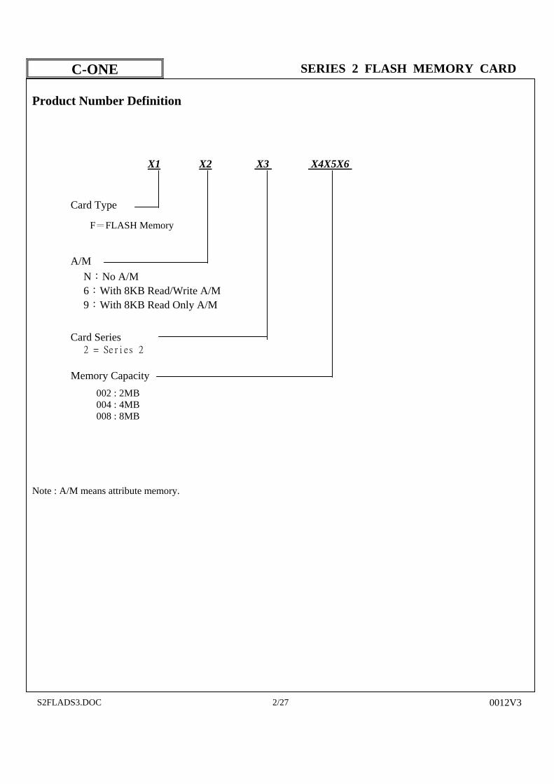
Product Number Definition
X1 X2 X3 X4X5X6
Card Type
F=FLASH Memory
A/M N:No A/M 6:With 8KB Read/Write A/M 9:With 8KB Read Only A/M
Card Series 2 = Series 2
Memory Capacity 002 : 2MB 004 : 4MB 008 : 8MB
Note : A/M means attribute memory.
C-ONE SERIES 2 FLASH MEMORY CARD
S2FLADS3.DOC 3/27 0012V3
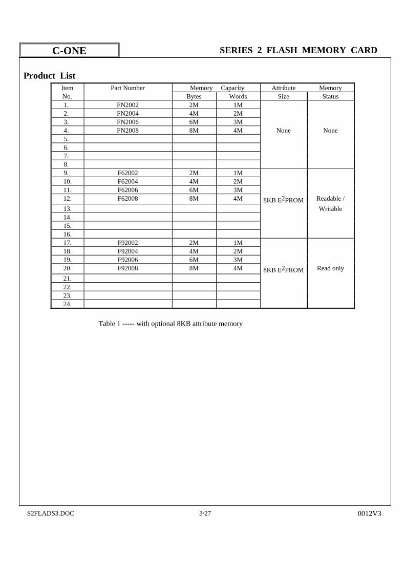
Product List Item Part Number Memory Capacity Attribute Memory No. Bytes Words Size Status 1. FN2002 2M 1M 2. FN2004 4M 2M 3. FN2006 6M 3M 4. FN2008 8M 4M None None 5. 6. 7. 8. 9. F62002 2M 1M 10. F62004 4M 2M 11. F62006 6M 3M 12. F62008 8M 4M 8KB E2PROM Readable / 13. Writable 14. 15. 16. 17. F92002 2M 1M 18. F92004 4M 2M 19. F92006 6M 3M 20. F92008 8M 4M 8KB E2PROM Read only 21. 22. 23. 24.
Table 1 ----- with optional 8KB attribute memory
C-ONE SERIES 2 FLASH MEMORY CARD
S2FLADS3.DOC 4/27 0012V3
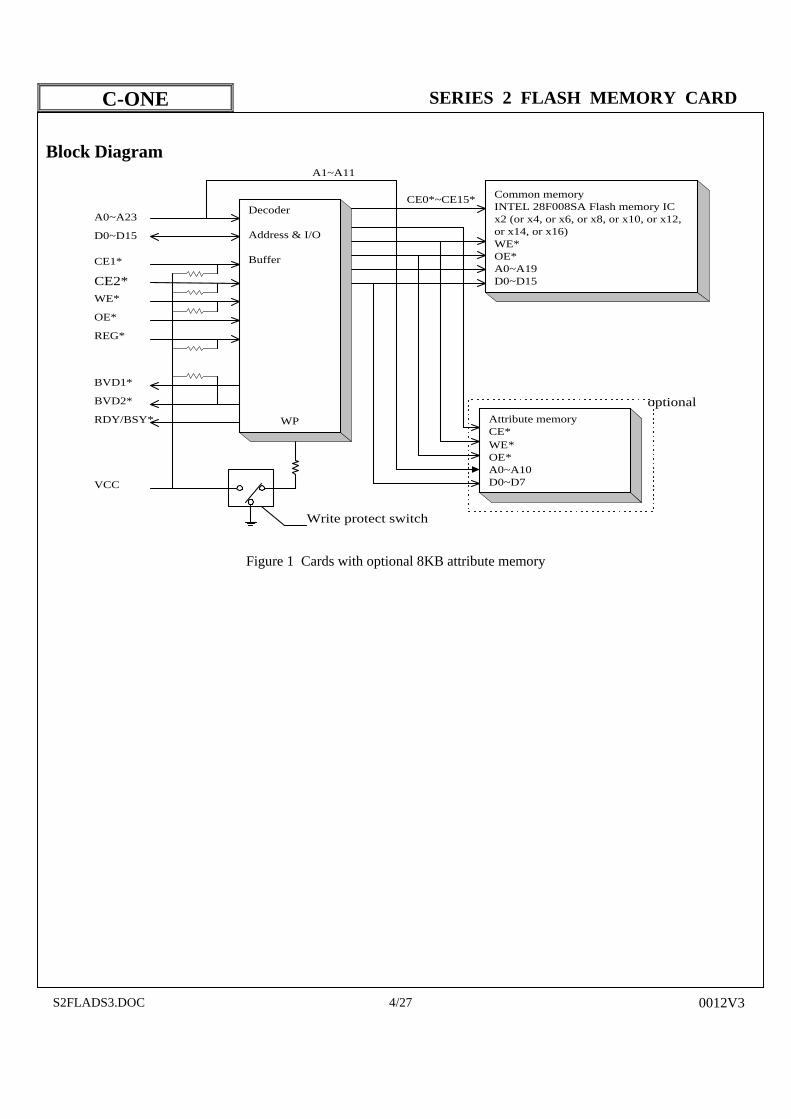
Block Diagram
A0~A23
D0~D15
CE1*
CE2*WE*
OE*
REG*
RDY/BSY*
BVD1*
BVD2*
VCC
Write protect switch
A1~A11
CE0*~CE15*
optional
Decoder
Address & I/O
Buffer
WP
Common memoryINTEL 28F008SA Flash memory ICx2 (or x4, or x6, or x8, or x10, or x12,or x14, or x16)WE*OE*A0~A19D0~D15
Attribute memoryCE*WE*OE*A0~A10D0~D7
Figure 1 Cards with optional 8KB attribute memory
C-ONE SERIES 2 FLASH MEMORY CARD
S2FLADS3.DOC 5/27 0012V3
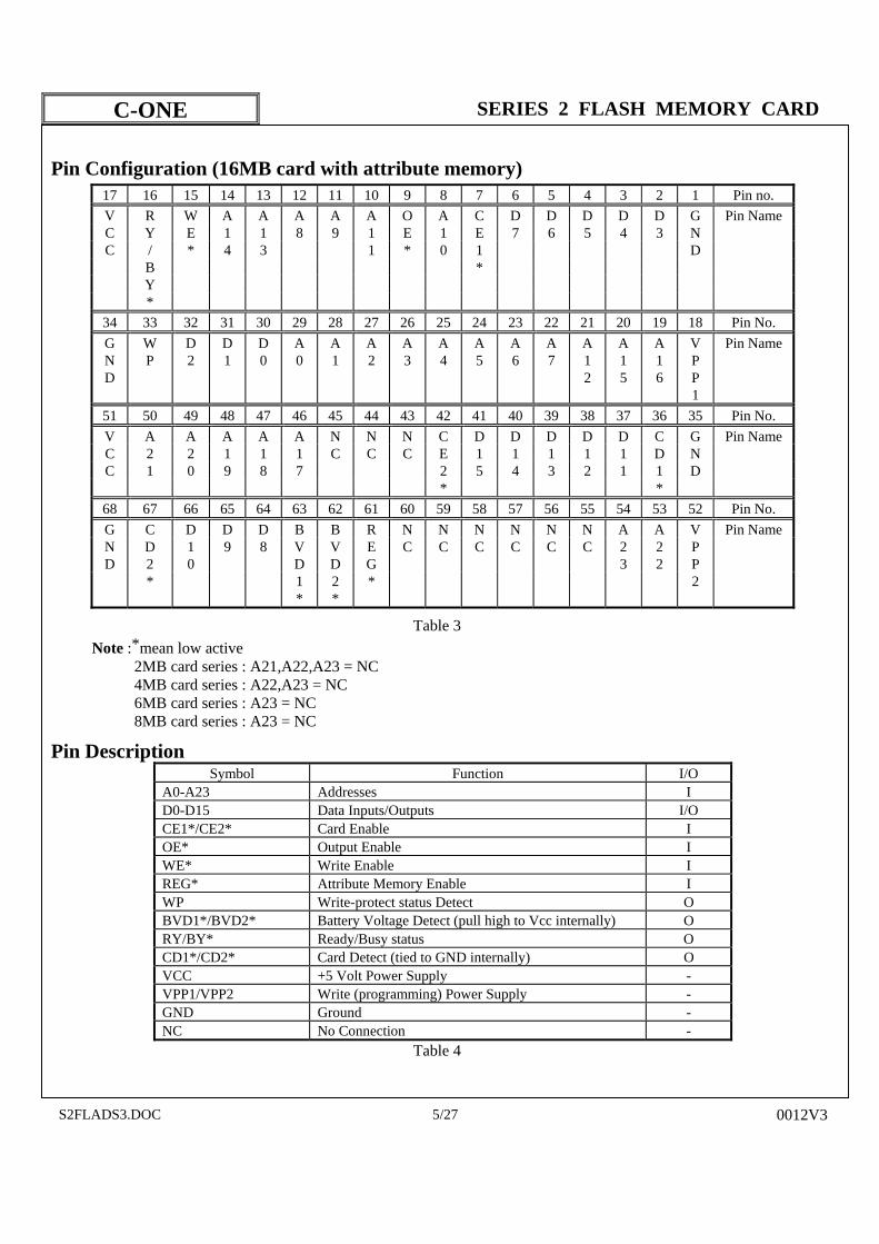
Pin Configuration (16MB card with attribute memory) 17 16 15 14 13 12 11 10 9 8 7 6 5 4 3 2 1 Pin no. V R W A A A A A O A C D D D D D G Pin NameC Y E 1 1 8 9 1 E 1 E 7 6 5 4 3 N C / * 4 3 1 * 0 1 D B * Y *
34 33 32 31 30 29 28 27 26 25 24 23 22 21 20 19 18 Pin No. G N D
W P
D 2
D 1
D0
A 0
A 1
A2
A3
A4
A5
A6
A7
A1 2
A 1 5
A 1 6
V P P 1
Pin Name
51 50 49 48 47 46 45 44 43 42 41 40 39 38 37 36 35 Pin No. V A A A A A N N N C D D D D D C G Pin NameC 2 2 1 1 1 C C C E 1 1 1 1 1 D N C 1 0 9 8 7 2 5 4 3 2 1 1 D * *
68 67 66 65 64 63 62 61 60 59 58 57 56 55 54 53 52 Pin No. G C D D D B B R N N N N N N A A V Pin NameN D 1 9 8 V V E C C C C C C 2 2 P D 2 0 D D G 3 2 P * 1 2 * 2 * *
Table 3 Note :*mean low active
2MB card series : A21,A22,A23 = NC 4MB card series : A22,A23 = NC 6MB card series : A23 = NC 8MB card series : A23 = NC
Pin Description Symbol Function I/O
A0-A23 Addresses I D0-D15 Data Inputs/Outputs I/O CE1*/CE2* Card Enable I OE* Output Enable I WE* Write Enable I REG* Attribute Memory Enable I WP Write-protect status Detect O BVD1*/BVD2* Battery Voltage Detect (pull high to Vcc internally) O RY/BY* Ready/Busy status O CD1*/CD2* Card Detect (tied to GND internally) O VCC +5 Volt Power Supply - VPP1/VPP2 Write (programming) Power Supply - GND Ground - NC No Connection -
Table 4
C-ONE SERIES 2 FLASH MEMORY CARD
S2FLADS3.DOC 6/27 0012V3
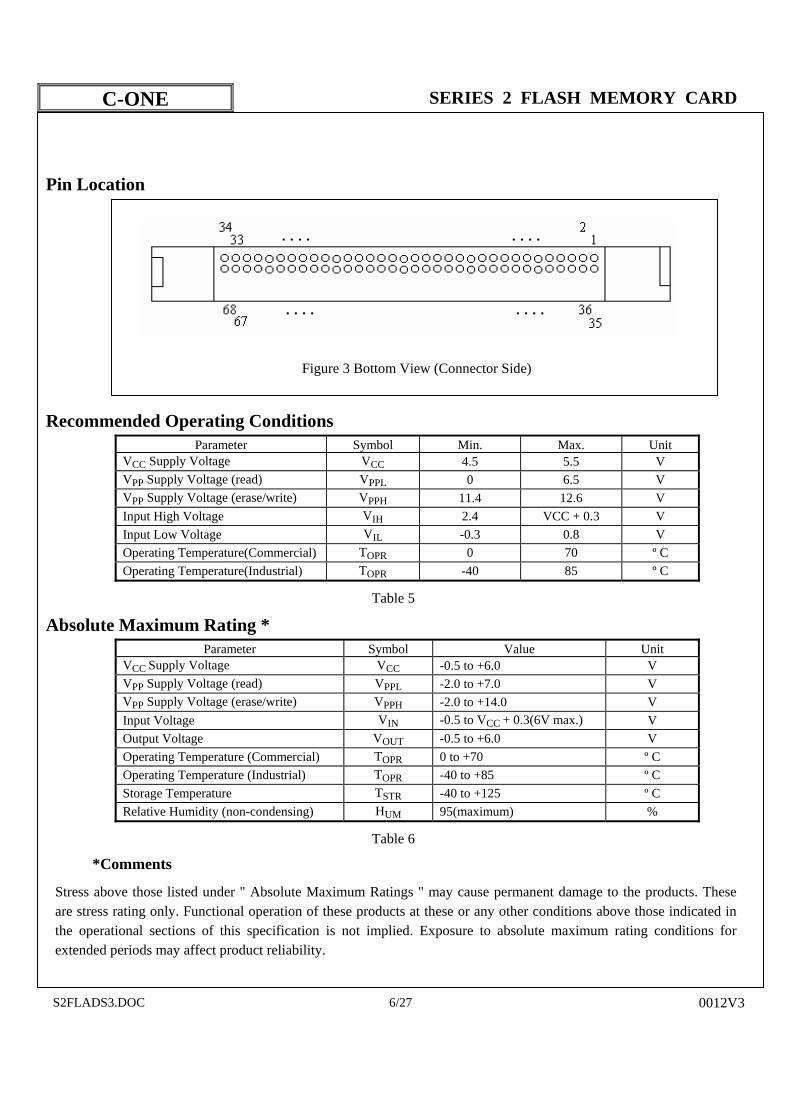
Pin Location
Figure 3 Bottom View (Connector Side)
Recommended Operating Conditions Parameter Symbol Min. Max. Unit
VCC Supply Voltage VCC 4.5 5.5 V VPP Supply Voltage (read) VPPL 0 6.5 V VPP Supply Voltage (erase/write) VPPH 11.4 12.6 V Input High Voltage VIH 2.4 VCC + 0.3 V Input Low Voltage VIL -0.3 0.8 V Operating Temperature(Commercial) TOPR 0 70 º C Operating Temperature(Industrial) TOPR -40 85 º C
Table 5
Absolute Maximum Rating * Parameter Symbol Value Unit
VCC Supply Voltage VCC -0.5 to +6.0 V VPP Supply Voltage (read) VPPL -2.0 to +7.0 V VPP Supply Voltage (erase/write) VPPH -2.0 to +14.0 V Input Voltage VIN -0.5 to VCC + 0.3(6V max.) V Output Voltage VOUT -0.5 to +6.0 V Operating Temperature (Commercial) TOPR 0 to +70 º C Operating Temperature (Industrial) TOPR -40 to +85 º C Storage Temperature TSTR -40 to +125 º C Relative Humidity (non-condensing) HUM 95(maximum) %
Table 6
*Comments
Stress above those listed under " Absolute Maximum Ratings " may cause permanent damage to the products. These are stress rating only. Functional operation of these products at these or any other conditions above those indicated in the operational sections of this specification is not implied. Exposure to absolute maximum rating conditions for extended periods may affect product reliability.
C-ONE SERIES 2 FLASH MEMORY CARD
S2FLADS3.DOC 7/27 0012V3
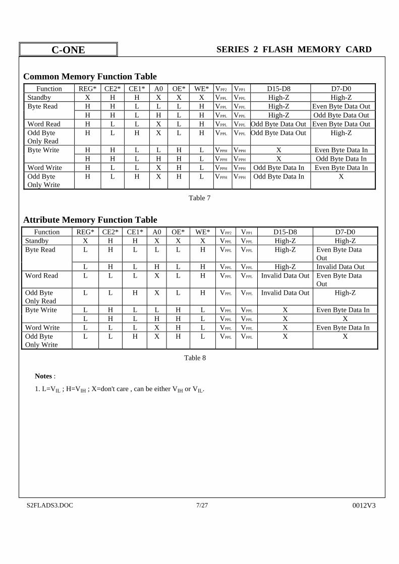
Common Memory Function Table Function REG* CE2* CE1* A0 OE* WE* VPP2 VPP1 D15-D8 D7-D0
Standby X H H X X X VPPL VPPL High-Z High-Z Byte Read H H L L L H VPPL VPPL High-Z Even Byte Data Out H H L H L H VPPL VPPL High-Z Odd Byte Data OutWord Read H L L X L H VPPL VPPL Odd Byte Data Out Even Byte Data OutOdd Byte Only Read
H L H X L H VPPL VPPL Odd Byte Data Out High-Z
Byte Write H H L L H L VPPH VPPH X Even Byte Data In H H L H H L VPPH VPPH X Odd Byte Data In Word Write H L L X H L VPPH VPPH Odd Byte Data In Even Byte Data In Odd Byte Only Write
H L H X H L VPPH VPPH Odd Byte Data In X
Table 7
Attribute Memory Function Table Function REG* CE2* CE1* A0 OE* WE* VPP2 VPP1 D15-D8 D7-D0
Standby X H H X X X VPPL VPPL High-Z High-Z Byte Read L H L L L H VPPL VPPL High-Z Even Byte Data
Out L H L H L H VPPL VPPL High-Z Invalid Data Out Word Read L L L X L H VPPL VPPL Invalid Data Out Even Byte Data
Out Odd Byte Only Read
L L H X L H VPPL VPPL Invalid Data Out High-Z
Byte Write L H L L H L VPPL VPPL X Even Byte Data In L H L H H L VPPL VPPL X X Word Write L L L X H L VPPL VPPL X Even Byte Data In Odd Byte Only Write
L L H X H L VPPL VPPL X X
Table 8 Notes :
1. L=VIL ; H=VIH ; X=don't care , can be either VIH or VIL.

C-ONE SERIES 2 FLASH MEMORY CARD
S2FLADS3.DOC 8/27 0012V3
Card Information Structure The Card Information Structure (CIS) starts from address zero of the card’s Attribute Memory. It contains a variable-length chain of data blocks (tuples). The table shown below is the generic CIS of C-ONE’s Series 2 Flash Memory Card. (For detailed tuple description, please refer to the Metaformat Specification of PC Card Standard.)
Tuple Address (Hex)
Data (Hex)
Description Tuple Address (Hex)
Data (Hex)
Description
00 01 CISTPL_DEVICE 18 52 R
02 03 TPL_LINK 1A 49 I
04 52 DEVICE_INFO = FLASH 200ns
1C 45 E
06 06 CARD SIZE 2MB 1E 53 S
0E 4MB 20 2D - (dash)
16 6MB 22 32 2
1E 8MB 24 20 SPACE
26 10MB 26 20 SPACE (for 2/4/6/8MB)
2E 12MB 31 1 (for 10/12/14/16MB)
36 14MB 28 30 0
3E 16MB 32 2
08 FF CISTPL_END 34 4
0A 15 CISTPL_VERS_1 36 6
0C 1F TPL_LINK 38 8
0E 04 TPLLV1_MAJOR 2A 4D M
10 01 TPLLV1_MINOR 2C 42 B
12 00 NULL 2E 20 SPACE
14 53 S 30 46 F
16 45 E 32 4C L
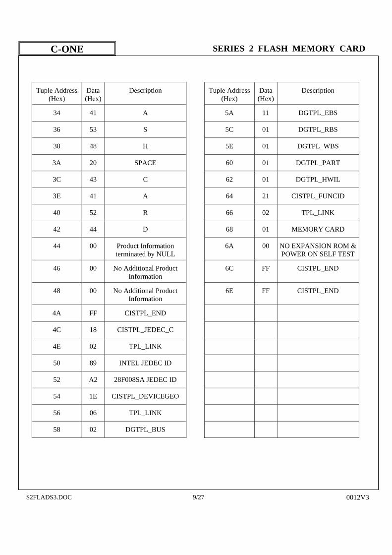
C-ONE SERIES 2 FLASH MEMORY CARD
S2FLADS3.DOC 9/27 0012V3
Tuple Address
(Hex) Data (Hex)
Description Tuple Address (Hex)
Data (Hex)
Description
34 41 A 5A 11 DGTPL_EBS
36 53 S 5C 01 DGTPL_RBS
38 48 H 5E 01 DGTPL_WBS
3A 20 SPACE 60 01 DGTPL_PART
3C 43 C 62 01 DGTPL_HWIL
3E 41 A 64 21 CISTPL_FUNCID
40 52 R 66 02 TPL_LINK
42 44 D 68 01 MEMORY CARD
44 00 Product Information terminated by NULL
6A 00 NO EXPANSION ROM & POWER ON SELF TEST
46 00 No Additional Product Information
6C FF CISTPL_END
48 00 No Additional Product Information
6E FF CISTPL_END
4A FF CISTPL_END
4C 18 CISTPL_JEDEC_C
4E 02 TPL_LINK
50 89 INTEL JEDEC ID
52 A2 28F008SA JEDEC ID
54 1E CISTPL_DEVICEGEO
56 06 TPL_LINK
58 02 DGTPL_BUS
C-ONE SERIES 2 FLASH MEMORY CARD
S2FLADS3.DOC 10/27 0012V3
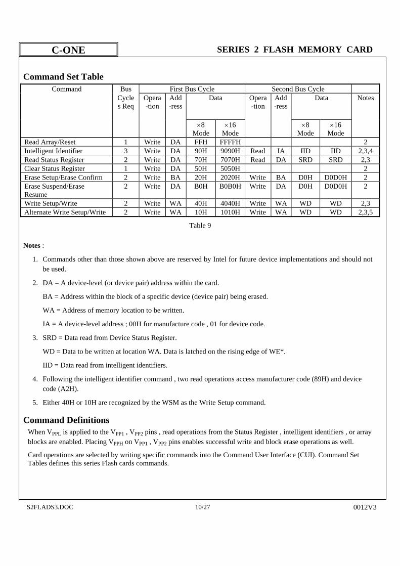
Command Set Table Command Bus First Bus Cycle Second Bus Cycle
Cycles Req
Opera-tion
Add-ress
Data
Opera-tion
Add-ress
Data Notes
×8 Mode
×16 Mode
×8 Mode
×16 Mode
Read Array/Reset 1 Write DA FFH FFFFH 2 Intelligent Identifier 3 Write DA 90H 9090H Read IA IID IID 2,3,4 Read Status Register 2 Write DA 70H 7070H Read DA SRD SRD 2,3 Clear Status Register 1 Write DA 50H 5050H 2 Erase Setup/Erase Confirm 2 Write BA 20H 2020H Write BA D0H D0D0H 2 Erase Suspend/Erase Resume
2 Write DA B0H B0B0H Write DA D0H D0D0H 2
Write Setup/Write 2 Write WA 40H 4040H Write WA WD WD 2,3 Alternate Write Setup/Write 2 Write WA 10H 1010H Write WA WD WD 2,3,5
Table 9 Notes :
1. Commands other than those shown above are reserved by Intel for future device implementations and should not be used.
2. DA = A device-level (or device pair) address within the card.
BA = Address within the block of a specific device (device pair) being erased.
WA = Address of memory location to be written.
IA = A device-level address ; 00H for manufacture code , 01 for device code.
3. SRD = Data read from Device Status Register.
WD = Data to be written at location WA. Data is latched on the rising edge of WE*.
IID = Data read from intelligent identifiers.
4. Following the intelligent identifier command , two read operations access manufacturer code (89H) and device code (A2H).
5. Either 40H or 10H are recognized by the WSM as the Write Setup command.
Command Definitions When VPPL is applied to the VPP1 , VPP2 pins , read operations from the Status Register , intelligent identifiers , or array blocks are enabled. Placing VPPH on VPP1 , VPP2 pins enables successful write and block erase operations as well.
Card operations are selected by writing specific commands into the Command User Interface (CUI). Command Set Tables defines this series Flash cards commands.
C-ONE SERIES 2 FLASH MEMORY CARD
S2FLADS3.DOC 11/27 0012V3
Read Array Command
Upon initial card powerup and after exit from deep powerdown mode , this series Flash cards default to the Read Array mode. This operation is also entered by writing FFH to the Command User Interface. Microprocessor read cycles retrieve array data. The card remains enabled for reads until the Command User Interface receives an alternate command. Once the internal Write State Machine has started a block-erase or data-write operation , the card will not recognize the Read Array command , until the WSM has completed its operation (or the Erase Suspend command is issued during erase). The Read Array command functions when VPP1 , VPP2 = VPPL or VPPH.
Intelligent Identifier Command
After executing this command , the intelligent Identifier values can be read. Only address A0 of each device is used in this mode , all other address inputs are ignored [(Manufacturer code=89H for A0=0) , (Device code=A2H (INTEL 28F008SA) for A0=1)]. The device will remain in this mode until the CUI receives another command.
This information is useful by system software in determining what type of flash memory device is contained within the card and allows the correct matching of device to write and erase algorithms. System software that fully utilizes the PCMCIA specification will not use the intelligent identifier mode , as this data is available within the Card Information Structure. The Intelligent Identifier command functions when VPP1 , VPP2 = VPPL or VPPH.
Read Status Register Command
After writing this command , a device read outputs the contents of its Status Register , regardless of the address presented to that device. The contents of this register are latched on the falling edge of OE* , CE1* (and/or CE2*) , whichever occurs last in the read cycle. This prevents possible bus errors which might occur if the contents of the Status Register changed while reading its contents. CE1* (and CE2* for odd-byte or word access) or OE* must be toggled with each subsequent status read , or the completion of a write or erase operation will not be evident. This command is executable while the WSM is operating , however , during a block-erase or data-write operation , reads from the device will automatically return status register data. Upon completion of that operation , the device remains in the Status Register read mode until the CUI receives another command. The Read Status Register command functions when VPP1 , VPP2 = VPPL or VPPH.
C-ONE SERIES 2 FLASH MEMORY CARD
S2FLADS3.DOC 12/27 0012V3
Clear Status Register Command
The Erase Status and Write Status bits are set to "1"s by the Write State Machine and can only be reset by the Clear Status Register Command. These bits indicate various failure conditions. By allowing system software to control the resetting of these bits , several operations may be performed (such as cumulatively writing several bytes or erasing multiple blocks in sequence). The Status Register may then be polled to determine if an error occurred during that sequence. This adds flexibility to the way the device may be used.
Additionally , the VPP Status bit (SR.3) MUST be reset by system software before further data writes or block erases are attempted. To clear the Status Register , the Clear Status Register command is written to the Command User Interface. The Clear Status Register command functions when VPP1 , VPP2 = VPPL or VPPH.
Erase Setup/Erase Confirm Commands
Within a device , erase is performed on one device block at a time , initiated by a two-cycle command sequence. After the system switches VPP to VPPH , an Erase Setup command (20H) prepares the CUI for the Erase Confirm command (D0H). The device's WSM controls the erase algorithms internally. After receiving the two-command erase sequence , the device automatically outputs Status Register data when read (See Figure 4). If the command after erase setup is not an Erase Confirm command , the CR sets the Write Failure and Erase Failure bits of the Status Register , places the device into the Read Status Register mode , and waits for another command. The Erase Confirm command enables the WSM for erase (simultaneously closing the address latches for that device's block (A16-A19 at the device level). The CPU detects the completion of the erase operation by analyzing card-level or device -level indicators. Card-level indicators include the RY/BY* pin and the READY-BUSY* Status Register ; while device-level indicators include the specific device's Status Register. Only the Read Status Register command is valid while the erase operation is active. Upon completion of the erase sequence (see section on Status Register) the device's Status Register reflects the result of the erase operation. The device remains in the Read Status Register mode until the CUI receives an alternate command.
The two-step block-erase sequence ensures that memory contents are not accidentally erased. Erase attempts while VPPL<VPP<VPPH produce spurious results and are not recommended. Reliable block erasure only occurs when VPP=VPPH. In the absence of this voltage , memory contents are protected against erasure. If block erase is attempted while VPP=VPPL , the VPP Status bit will be set to "1".
When erase completes , the Erase Status bit should be checked. If an erase error is detected , the device's Status Register should be cleared. The CUI remains in Read Status Register mode until receiving an alternate command.
C-ONE SERIES 2 FLASH MEMORY CARD
S2FLADS3.DOC 13/27 0012V3
Erase Suspend/Erase Resume Commands
Erase Suspend allows block erase interruption in order to read data from another block of the device or to temporarily conserve power for another system operation. Once the erase process starts , writing the Erase Suspend command to the CUI (See Figure 5) requests the WSM to suspend the erase sequence at a predetermined point in the erase algorithm. In the erase suspend state , the device continues to output Status Register data when read.
Polling the device's RY/BY* and Erase Suspend Status bits (Status Register) , or the card's READY-BUSY* Status Register for that particular device , will determine when the erase suspend mode is valid. It is important to note that the card's RY/BY* pin will also transition to VOH and will generate an interrupt if this pin is connected to a system-level interrupt. At this point , a Read Array command can be written to the device's CUI to read data from blocks other than that which is suspended. The only other valid commands at this time are Read Status Register (70H) and Erase Resume (D0H). If VPP goes low during Erase Suspend , the VPP Status bit is set in the Status Register.
The Erase Resume command clears the Erase Suspend state and allows the WSM to continue with the erase operation. The device's RY/BY* Status and Erase Suspend Status bits and the card's READY-BUSY* Status Register are automatically updated to reflect the erase resume condition. The card's RY/BY* pin also returns to VOL.
Write Setup/Write Commands
A data-write operation is executed by a two-command sequence. After the system switches VPP to VPPH , the write setup command (40H) is written to the CUI of the appropriate device , followed by a second write specifying the address and write data (latched on the rising edge of WE*). The device's WSM controls the data-write and write verify algorithms internally. After receiving the two-command write sequence , the device automatically outputs Status Register data when read (See Figure 3). The CPU detects the completion of the write operation by analyzing card-level or device-level indicators. Card-level indicators include the RY/BY* pin and the READY-BUSY* Status Register ; while device-level indicators include the specific device's Status Register. Only the Read Status Register command is valid while the write operation is active. Upon completion of the data-write sequence (see section on Status Register) the device's Status Register reflects the result of the write operation. The device remains in the Read Status Register mode until the CUI receives an alternate command.

C-ONE SERIES 2 FLASH MEMORY CARD
S2FLADS3.DOC 14/27 0012V3
Device Status Register Definition
Each 28F008SA device in this Series 2 Card contains a Status Register which displays the condition of its Write State Machine. The Status Register is read at any time by writing the Read Status command to the CUI. After writing this command , all subsequent Read operations output data from the Status Register , until another command is written to the CUI.
Bit 7 Bit 6 Bit 5 Bit 4 Bit 3 Bit 2 Bit 1 Bit 0 WSMS ESS ES BWS VPPS R R R
Table 10
Bit 7 --- WAM Status This bit reflects the Ready/Busy* condition of the WSM. A '1' indicates that read , block-erase or data-write operations are available. A '0' indicates that write or erase operations are in progress.
Bit 6 --- Erase Suspend Status If an Erase Suspend command is issued during the erase operation , the WSM halts execution and sets the WSM Status bit and the Erase Suspend Status bit to a '1'. This bit remains set until the device receives an Erase Resume command , at which point the CUI resets the WSM Status bit and the Erase Suspend Status bit.
Bit 5 --- Erase Status This bit will be cleared to 0 to indicate a successful block-erasure. When set to a '1' , the WSM has been unsuccessful at performing an erase verification. The device's CUI only resets this bit to a '0' in response to a Clear Status Register command.
Bit 4 --- Write Status This bit will be cleared to a 0 to indicate a successful data-write operation. When the WSM fails to write data after receiving a write command , the bit is set to a '1' and can only be reset by the CUI in response to a Clear Status Register command.
Bit 3 --- VPP Status During block-erase and data-write operations , the WSM monitors the output of the device's internal VPP detector. In the event of low VPP , the WSM sets ('1') the VPP Status bit , the status bit for the operation in progress (either write or erase). The CUI resets these bits in response to a Clear Status Register command . Also , the WSM RY/BY* bit will be set to indicate a device ready condition. This bit MUST be reset by system software (Clear Status Register command) before further data writes or block erases are attempted.
Bit 2 , Bit 1 , Bit 0 --- Reserved for future enhancements These bits are reserved for future use and should be masked out when polling the Status Register.

C-ONE SERIES 2 FLASH MEMORY CARD
S2FLADS3.DOC 15/27 0012V3
Device -- Level Automated Write Algorithm
Full Status Check Procedure
Status Register DataRead (See Above)
VppLevel OK
DataWrite OK
YES
Data WriteSuccessful
Vpp Range5Error
Data WriteError
6
NO
NO
YES
?
?
Figure 4
Start
Issue Write Setup1
Command
Write Data
Read StatusRegister
2
DoneWriting Data
Full StatusCheck If Desired
3
Write OperationComplete
4
NO
YES
?
Bus Operation
Command
x8 Mode
x16 Mode
Write
Write Setup
Data=40H Address=Byte Within Card to be Written
Data=4040H Address=Word Within Card to be Written
Write
Data Write
Data to be Written Address=Byte Within Card to be Written
Data to be Written Address=Word Within Card to be Written
Read
Defaults to Device StatusRegister ReadMode
Status Register Data. Toggle OE* CE1* or CE2* to update Status Register
Status Register Data. Toggle OE* or (CE1* and CE2*) to update Status Registers
Standby
Check SR Bit 7 1=Ready, 0=Busy
Check SR Bits 7&15 1=Ready, 0=Busy
Bus Command x8 Mode x16 Mode Operation Standby Check SR Bit 3 Check SR Bits 3&11
1=VPP Detected Low
1=VPP Detected Low
Standby Check SR Bit 4 Check SR Bits 4&12 1=Data Write Error 1=Data Write Error

C-ONE SERIES 2 FLASH MEMORY CARD
S2FLADS3.DOC 16/27 0012V3
Device--Level Automated Erase Algorithm
Full Status Check Procedure
Figure 5
Start
Write Erase Setup 1
Command
Write Erase Confirm
Read StatusRegister
2
EraseDone
Full StatusCheck If Desired
3
Block EraseCompleted
4
NO
YES
Command
NO
Suspend EraseLoop
YESSuspendErase
? ?
Bus Operation
Command
x8 Mode
x16 Mode
Write
Erase Setup
Data=20H, Address=Block Within Card to be Erased
Data=2020H, Address=Block pair Within Card to be Erased
Write
Erase
Data=D0H, Address=Block Within Card to be Erased
Data=D0D0H, Address=Block Pair Within Card to be Erased
Read
Defaults to Device Sta- tus Register Read Mode
Status Register Data. Toggle OE* CE1* or CE2* to update Status Register
Status Register Data. Toggle OE* or (CE1* and CE2*) to update Status Register
Standby
Check SR Bit 7 1=Ready, 0=Busy
Check SR Bits 7&15 1=Ready, 0=Busy
Status Register DataRead (See Above)
VppLevel OK
Sequence
YES
Vpp Range 5
Error
Command SequenceError
NO
NO
YES
BlockErase OK
Block EraseError
6NO
Block EraseSuccessful
Command
OK ?
NO
?
?
Bus Operation
Command
x8 Mode
x16 Mode
Standby Check SR Bit 3 1=VPP Detected Low
Check SR Bits 3&11 Either bit 1=VPP Detected Low
Standby
Check SR Bits 4&5 Both 1=Command Sequence Error
Check SR Bit 4,5,12,13All 1=Command Sequence Error
Standby
Check SR Bit 5 1=Block Erase Error
Check SR Bits 5&13 Both 1=Block Erase Failure

C-ONE SERIES 2 FLASH MEMORY CARD
S2FLADS3.DOC 17/27 0012V3
Erase Suspend/Resume Algorithm
Write EraseSuspend
Read StatusRegister Data
A
WSMBusy
EraseSuspended
Write ReadArray Cmd
Read ArrayData
DoneReading
Write ResumeCommand
Return
YES
NO
NO
YES
Increment toNext Address
NO
YES
?
?
?
Figure 5 Figure 6
Bus Operation
Command
x8 Mode
x16 Mode
Write
Suspend Erase
Data=B0H Address=Desired Block to Erase Suspend
Data=B0B0H, Address=Desired Block Pair to Erase Suspend
Read
Status Register Data. Toggle OE* CE1* or CE2* to update Status Register
Status Register Data. Toggle OE* or (CE1* and CE2*) to update Status Register
Standby
Check SR Bit 7 1=Ready, 0=Busy
Check SR Bit 7&15 1=Ready, 0=Busy
Standby
Check SR Bit 6 1=Suspended, 0=In Progress
Check SR Bit 6&14 1=Suspended, 0=In Progress
Write
Read Array Cmd
Data=FFH
Data-FFFFH
Read
Read Data until finished
Read Data until finished
Write
Erase Resume
Data=D0H, Address=Valid Block Address.
Data-D0D0H, Address=Valid Block Pair Address.
C-ONE SERIES 2 FLASH MEMORY CARD
S2FLADS3.DOC 18/27 0012V3
DC Electrical Characteristics (recommended operating conditions unless otherwise noted)
Symbol Parameter 8-Bit Mode 16-Bit Mode Unit Test Condition min max min max
ILI Input Leakage Current -10 10 -10 10 uA VIN = 0V to VCC (Note 1) -70 10 -70 10 uA VIN = 0V to VCC (Note 2)
ILO Output Leakage Current -10 10 -10 10 uA CE1* = CE2* = VIH or OE* = VIH , VOUT = 0V to VCC (Note 3)
VIH Input High Voltage 2.4 VCC+0.3 2.4 VCC+0.3
V
VIL Input Low Voltage -0.3 0.8 -0.3 0.8 V VOH Output High Voltage 3.8 3.8 V IOH = -2.0mA (Note 4) VOL Output Low Voltage 0.4 0.4 V IOL = 3.2mA (Note 4) ICCR VCC Read Current 60 110 mA Min. cycle , IOUT = 0mA ICCW VCC Write Current 40 70 mA Write in progress ICCE VCC Erase Current 40 70 mA Block (pair) Erase in
progress ICCES VCC Erase Suspend Current 10 20 mA Erase suspended ICCS VCC Standby Current 1.5 1.5 mA CE1* = CE2* = VIH or
覓CC-0.2V
IPPR VPP Read Current 0.8 1.0 mA VPP > VCC IPPW VPP Write Current 30 60 mA Write in progress IPPE VPP Erase Current 30 60 mA Block (pair) Erase in
progress IPPES VPP Erase Suspend Current 0.4 0.8 mA Erase Suspended IPPS VPP Standby Current 30 30 uA VPP ™CC VPPL VPP During Read Only
Operation 0 6.5 0 6.5 V
VPPH VPP During Erase / Write Operation
11.4 12.6 11.4 12.6 V
Table 11
Note : 1.) Except CE1* , CE2* , WE* , REG* pins. 2.) For CE1* , CE2* , WE* , REG* pins. 3.) Except BVD1* , BVD2* , CD1* , CD2* pins. 4.) Except CD1* , CD2* pins.
C-ONE SERIES 2 FLASH MEMORY CARD
S2FLADS3.DOC 19/27 0012V3
AC Electrical Characteristics (recommended operating conditions unless otherwise noted)
Read Cycle (Common Memory) Symbol Parameter Note
s Min Max Unit
tAVAV tRC Read Cycle Time 200 ns
tAVQV ta (A) Address Access Time 200 ns
tELQV ta (CE) Card Enable Access Time 200 ns
tGLQV ta (OE) Output Enable Access Time 100 ns
tEHQX tdis (CE) Output Disable Time (CE*) 90 ns
tGHQZ tdis (OE) Output Disable Time (OE*) 90 ns
tGLQX ten (CE) Output Enable Time (CE*) 5 ns
tELQX ten (OE) Output Enable Time (OE*) 5 ns
tAXQX tv (A) Data Valid from Address Change 0 ns
Table 12
Write Cycle (Common Memory) Symbol Parameter Note
s Min Max Unit
tAVAV twc Write Cycle Time 200 ns tWLWH tw (WE) Write Pulse Width 100 ns tAVWL tsu (A) Address Setup Time 10 ns tAVWH tsu (A-WEH) Address Setup Time for WE* 140 ns tVPWH tvps VPP Setup to WE* Going High 100 ns tELWH tsu (CE-WEH) Card Enable Setup Time for WE* 140 ns tDVWH tsu (D-WEH) Data Setup Time for WE* 60 ns tWHDX th (D) Data Hold Time 30 ns tWHAX trec (WE) Write Recover Time 30 ns tWHRL WE High to RY/BY* 120 ns tWHQV1
Duration of Data Write Operation 6 us
tWHQV2
Duration of Block Erase Operation 0.3 sec
tQVVL VPP Hold from Operation Complete
2 0 ns
tWHGL th (OE-WE) Write Recovery before Read 10 ns
Table 13 Notes : 1. Read timing characteristics during erase and data write operation are the same as during read-only operations. Refer to
AC Characteristics for Read-Only operations.

C-ONE SERIES 2 FLASH MEMORY CARD
S2FLADS3.DOC 20/27 0012V3
Write Cycle (Common Memory) (CE* controlled)
Symbol Parameter Notes
Min Max Unit
tAVAV twc Write Cycle Time 1 200 ns
tELEH tw (WE) Card Enable Pulse Width 1 120 ns
tAVEL tsu (A) Address Setup Time 1 20 ns
tAVEH tsu (A-WEH) Address Setup Time for CE* 1 140 ns
tVPEH tvps VPP Setup to CE* Going High 1 100 ns
tWLEH tsu (CE-WEH) Write Enable Setup Time for CE* 1 140 ns
tDVEH tsu (D-WEH) Data Setup Time for CE* 1 60 ns
tEHDX th (D) Data Hold Time 1 30 ns
tEHAX trec (WE) Write Recover Time 1 30 ns
tEHRL CE* High to RY/BY* 1 120 ns
tEHQV1 Duration of Data Write
Duration of Data Write Operation 1 6 us
tEHQV2 Duration of Erase
Duration of Block Erase Operation 1 0.3 sec
tQVVL VPP Hold from Operation Complete 1,2 0 ns
tEHGL th (OE-WE) Write Recovery before Read 1 10 ns
Table 14
Notes :
1. Read timing characteristics during erase and data write operation are the same as during read-only operations. Refer to AC Characteristics for Read-Only operations.
2. Refer to text on Data-Write and Block-Erase Operations.
C-ONE SERIES 2 FLASH MEMORY CARD
S2FLADS3.DOC 21/27 0012V3
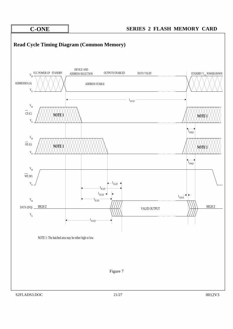
Read Cycle Timing Diagram (Common Memory)
DEVICE ANDADDRESS SELECTION OUTPUTS ENABLED DATA VALID
ADDRESS STABLEADDRESSES (A)
VIH
VIL
VCC POWER-UP STANDBY STANDBY VCC POWER-DOWN
tAVAV
NOTE 1
NOTE 1
CE (C)
VIH
VIL
NOTE 1
VIH
VIL
OE (G)NOTE 1
tGHQZ
VIH
VIL
WE (W)
tGHQZ
HIGH Z
tAXOXtELQX
tGLQX
tELQV
tGLQV
tAVQV
VIH
VIL
DATA (D/Q) HIGH Z VALID OUTPUT
NOTE 1: The hatched area may be either high or low.
Figure 7
C-ONE SERIES 2 FLASH MEMORY CARD
S2FLADS3.DOC 22/27 0012V3
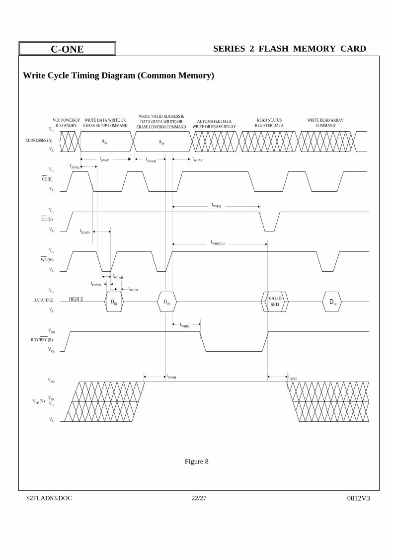
Write Cycle Timing Diagram (Common Memory)
WRITE DATA WRITE ORERASE SETUP COMMAND
WRITE VALID ADDRESS &DATA (DATA WRITE) OR
ERASE CONFIRM COMMANDAUTOMATED DATA
WRITE OR ERASE DELAY
ADDRESSES (A)
VIH
VIL
VCC POWER-UP& STANDBY
WRITE READ ARRAYCOMMAND
tAVAV
CE (E)
VIH
VIL
VIH
VIL
OE (G)
tWHGL
VIH
VIL
WE (W)
tWHDX
tDVWH
tWLWH
tWHRL
VIH
VIL
DATA (D/Q) HIGH Z
READ STATUSREGISTER DATA
tAVWHtWHAX
tAVWL
tWHQV1,2
DINVALID
SRDDINDIN
VOL
RDY/BSY (R)
VOH
VPPH
VPPLVPP (V) VIH
VIL
tVPWH tQVVL
tELWH
AIN AIN
Figure 8
C-ONE SERIES 2 FLASH MEMORY CARD
S2FLADS3.DOC 23/27 0012V3
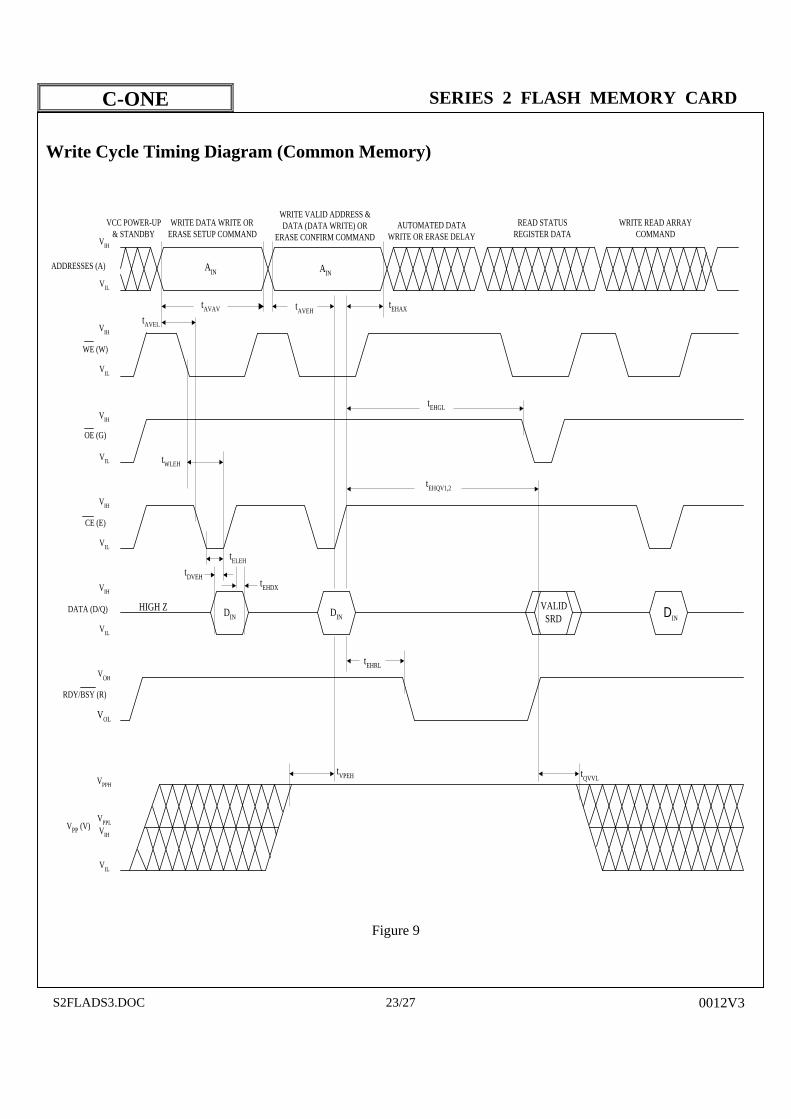
Write Cycle Timing Diagram (Common Memory)
WRITE DATA WRITE ORERASE SETUP COMMAND
WRITE VALID ADDRESS &DATA (DATA WRITE) OR
ERASE CONFIRM COMMANDAUTOMATED DATA
WRITE OR ERASE DELAY
ADDRESSES (A)
VIH
VIL
VCC POWER-UP& STANDBY
WRITE READ ARRAYCOMMAND
tAVAV
WE (W)
VIH
VIL
VIH
VIL
OE (G)
tEHGL
VIH
VIL
CE (E)
tEHDX
tDVEH
tELEH
tEHRL
VIH
VIL
DATA (D/Q) HIGH Z
READ STATUSREGISTER DATA
tAVEHtEHAX
tAVEL
tEHQV1,2
DINVALID
SRDDINDIN
VOL
RDY/BSY (R)
VOH
VPPH
VPPLVPP (V) VIH
VIL
tVPEH tQVVL
tWLEH
AIN AIN
Figure 9

C-ONE SERIES 2 FLASH MEMORY CARD
S2FLADS3.DOC 24/27 0012V3
Block Erase and Data Write Performance
Parameter Min. Typ. Max. Unit Notes Block Pair Erase Time 1.6 10 sec 2 Block Pair Write Time 0.6 2.1 sec 2
Table 15
Notes : 1. Individual blocks can be erased 100000 times. 2. Excludes System-Level Overhead. 3. Typical condition is 25º C , 12.0V VPP.
C-ONE SERIES 2 FLASH MEMORY CARD
S2FLADS3.DOC 25/27 0012V3
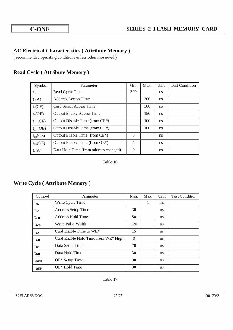
AC Electrical Characteristics ( Attribute Memory ) ( recommended operating conditions unless otherwise noted )
Read Cycle ( Attribute Memory )
Symbol Parameter Min. Max. Unit Test Conditiontcr Read Cycle Time 300 ns
ta(A) Address Access Time 300 ns
ta(CE) Card Select Access Time 300 ns
ta(OE) Output Enable Access Time 150 ns
tdis(CE) Output Disable Time (from CE*) 100 ns
tdis(OE) Output Disable Time (from OE*) 100 ns
ten(CE) Output Enable Time (from CE*) 5 ns
ten(OE) Output Enable Time (from OE*) 5 ns
tv(A) Data Hold Time (from address changed) 0 ns
Table 16
Write Cycle ( Attribute Memory )
Symbol Parameter Min. Max. Unit Test Conditiontcw Write Cycle Time 1 ms
tAS Address Setup Time 30 ns
tAH Address Hold Time 50 ns
tWP Write Pulse Width 120 ns
tCS Card Enable Time to WE* 15 ns
tCH Card Enable Hold Time from WE* High 0 ns
tDS Data Setup Time 70 ns
tDH Data Hold Time 30 ns
tOES OE* Setup Time 30 ns
tOEH OE* Hold Time 30 ns
Table 17

C-ONE SERIES 2 FLASH MEMORY CARD
S2FLADS3.DOC 26/27 0012V3
Read Cycle Timing Diagram ( Attribute Memory ) ( REG*=VIL , WE*=VIH )
Addresstcr
t
t
t
tt
t
DATA VALID
t
t
Data Out
OE*
CE2*CE1* or/and
(A1-A11)
en(CE)
en(OE)
a(OE)
a(CE)
a(A)
dis(OE)
dis(CE)
v(A)
Figure 10
Write Cycle Timing Diagram ( Attribute Memory ) ( REG*=VIL )
Address
OE*
CE2*CE1* or/and
DATA INPUT VALID
WE*
Data In
(A1-A11)t AH
t AS
tWP
tOEH
ttOES
t DS
h(D)
t CS t CH
Figure 11
C-ONE SERIES 2 FLASH MEMORY CARD
S2FLADS3.DOC 27/27 0012V3
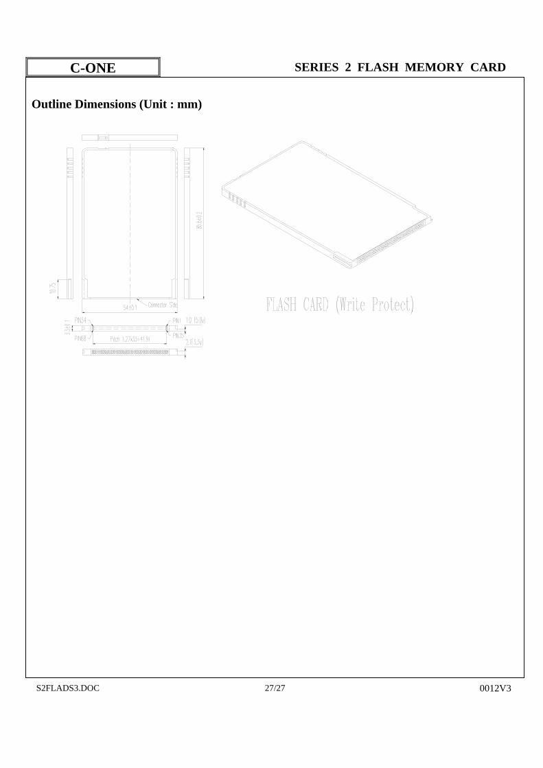
Outline Dimensions (Unit : mm)