lin transceiver atmel - digi-key sheets/atmel pdfs/ata6662(c).pdf · 3 4916p–auto–10/11 atmel...
TRANSCRIPT

LIN Transceiver
Atmel ATA6662ATA6662C
4916P–AUTO–10/11
Features• Operating Range from 5V to 27V• Baud Rate up to 20 Kbaud• Improved Slew Rate Control According to LIN Specification 2.0, 2.1 and SAEJ2602-2• Fully Compatible with 3.3V and 5V Devices• Dominant Time-out Function at Transmit Data (TXD)• Normal and Sleep Mode• Wake-up Capability via LIN Bus (90µs Dominant)• External Wake-up via WAKE Pin (35µs Low Level)• Control of External Voltage Regulator via INH Pin• Very Low Standby Current During Sleep Mode (10 µA)• Wake-up Source Recognition• Bus Pin Short-circuit Protected versus GND and Battery• LIN Input Current < 2µA if VBAT Is Disconnected• Overtemperature Protection• High EMC Level• Interference and Damage Protection According to ISO/CD 7637• Fulfills the OEM “Hardware Requirements for LIN in Automotive Applications Rev.1.0”
1. DescriptionThe Atmel® ATA6662 is a fully integrated LIN transceiver complying with the LINspecification 2.0, 2.1 and SAEJ2602-2. It interfaces the LIN protocol handler and thephysical layer. The device is designed to handle the low-speed data communication invehicles, for example, in convenience electronics. Improved slope control at the LINdriver ensures secure data communication up to 20Kbaud. Sleep Mode guaranteesminimal current consumption. The Atmel ATA6662 has advanced EMI and ESDperformance.
Figure 1-1. Block Diagram
VS
GND5
6 LIN
7
1
4
RXD
TXD
WAKE
EN
3
2 8
INH
Short-circuit and over-temperature protection
Receiver
Filter
Wake-up bus timer
Slew rate controlTXD
time-outtimer
VS
Wake-uptimer Sleep mode
VS
Control unit
+

2. Pin Configuration
Figure 2-1. Pinning SO8
RXDEN
WAKETXD
INHVSLINGND
1234
8765
Table 2-1. Pin Description
Pin Symbol Function
1 RXD Receive data output (open drain)
2 EN Enables Normal Mode; when the input is open or low, the device is in Sleep Mode
3 WAKE High voltage input for local wake-up request. If not needed, connect directly to VS
4 TXD Transmit data input; active low output (strong pull-down) after a local wake-up request
5 GND Ground, heat sink
6 LIN LIN bus line input/output
7 VS Battery supply
8 INHBattery-related inhibit output for controlling an external voltage regulator; active high after a wake-up request
24916P–AUTO–10/11
Atmel ATA6662/ATA6662C

Atmel ATA6662/ATA6662C
3. Functional Description
3.1 Physical Layer CompatibilitySince the LIN physical layer is independent from higher LIN layers (e.g., the LIN protocollayer), all nodes with a LIN physical layer according to revision 2.x can be mixed with LINphysical layer nodes, which, according to older versions (i.e., LIN 1.0, LIN 1.1, LIN 1.2, LIN1.3), are without any restrictions.
3.2 Supply Pin (VS)Undervoltage detection is implemented to disable transmission if VS falls to a value below 5Vin order to avoid false bus messages. After switching on VS, the IC switches to Fail-safe Modeand INHIBIT is switched on. The supply current in Sleep Mode is typically 10µA.
3.3 Ground Pin (GND)The Atmel® ATA6662 does not affect the LIN Bus in the case of a GND disconnection. It isable to handle a ground shift up to 11.5% of VS.
3.4 Bus Pin (LIN)A low-side driver with internal current limitation and thermal shutdown and an internal pull-upresistor are implemented as specified for LIN 2.x. The voltage range is from –27V to +40V.This pin exhibits no reverse current from the LIN bus to VS, even in the case of a GND shift orVBatt disconnection. The LIN receiver thresholds are compatible to the LIN protocol specifica-tion.The fall time (from recessive to dominant) and the rise time (from dominant to recessive)are slope controlled. The output has a self-adapting short circuit limitation; that is, during cur-rent limitation, as the chip temperature increases, the current is reduced.
3.5 Input/Output Pin (TXD)In Normal Mode the TXD pin is the microcontroller interface to control the state of the Lin out-put. TXD must be at Low- level in order to have a low LIN Bus. If TXD is high, the LIN outputtransistor is turned off and the Bus is in recessive state. The TXD pin is compatible to both a3.3V or 5V supply. During fail-safe Mode, this pin is used as output and is signalling thewake-up source (see Section 3.14 “Wake-up Source Recognition” on page 8). It is current lim-ited to < 8 mA.
3.6 TXD Dominant Time-out FunctionThe TXD input has an internal pull-down resistor. An internal timer prevents the bus line frombeing driven permanently in dominant state. If TXD is forced to low longer than tDOM > 6ms,the pin LIN will be switched off (Recessive Mode). To reset this mode, switch TXD to high(> 10µs) before switching LIN to dominant again.
3.7 Output Pin (RXD)This pin reports to the microcontroller the state of the LIN bus. LIN high (recessive) is reportedby a high level at RXD, LIN low (dominant) is reported by a low voltage at RXD. The output isan open drain, therefore, it is compatible to a 3.3V or 5V power supply. The AC characteristicsare defined with a pull-up resistor of 5kΩ to 5V and a load capacitor of 20pF. The output isshort-protected. In Unpowered Mode (VS = 0V), RXD is switched off. For ESD protection aZener diode is integrated, with VZ = 6.1V.
34916P–AUTO–10/11
3.8 Enable Input Pin (EN)This pin controls the Operation Mode of the interface. If EN = 1, the interface is in NormalMode, with the transmission path from TXD to LIN and from LIN to RXD both active. At a fall-ing edge on EN, while TXD is already set to high, the device is switched to Sleep Mode and notransmission is possible. In Sleep Mode, the LIN bus pin is connected to VS with a weakpull-up current source. The device can transmit only after being woken up (see Section 3.9,“Inhibit Output Pin (INH)” ).
During Sleep Mode the device is still supplied from the battery voltage. The supply current istypically 10µA. The pin EN provides a pull-down resistor in order to force the transceiver intoSleep Mode in case the pin is disconnected.
3.9 Inhibit Output Pin (INH)This pin is used to control an external switchable voltage regulator having a wake-up input.The inhibit pin provides an internal switch towards pin VS. If the device is in Normal Mode, theinhibit high-side switch is turned on and the external voltage regulator is activated. When thedevice is in Sleep Mode, the inhibit switch is turned off and disables the voltage regulator.
A wake-up event on the LIN bus or at pin WAKE will switch the INH pin to the VS level. After asystem power-up (VS rises from zero), the pin INH switches automatically to the VS level.
3.10 Wake-up Input Pin (WAKE)This pin is a high-voltage input used to wake the device up from Sleep Mode. It is usuallyconnected to an external switch in the application to generate a local wake-up. A pull-up cur-rent source with typically –10µA is implemented. The voltage threshold for a wake-up signal is3V below the VS voltage with an output current of typically –3µA.
If you do not need a local wake-up in your application, connect pin WAKE directly to pin VS.
44916P–AUTO–10/11
Atmel ATA6662/ATA6662C

Atmel ATA6662/ATA6662C
3.11 Operation Modes1. Normal Mode
This is the normal transmitting and Receiving Mode. All features are available.
2. Sleep ModeIn this mode the transmission path is disabled and the device is in low power mode. Supply current from VBatt is typically 10µA. A wake-up signal from the LIN bus or via pin WAKE will be detected and will switch the device to Fail-safe Mode. If EN then switches to high, Normal Mode is activated. Input debounce timers at pin WAKE (tWAKE), LIN (tBUS) and EN (tsleep,tnom) prevent unwanted wake-up events due to auto-motive transients or EMI. In Sleep Mode the INH pin is left floating. The internal termination between pin LIN and pin VS is disabled. Only a weak pull-up current (typ-ical 10µA) between pin LIN and pin VS is present. The Sleep Mode can be activated independently from the actual level on pin LIN or WAKE.
3. Fail-safe ModeAt system power-up or after a wake-up event, the device automatically switches to Fail- safe Mode. It switches the INH pin to a high state, to the VS level. LIN communi-cation is switched off. The microcontroller of the application will then confirm the Normal Mode by setting the EN pin to high.
4. Unpowered ModeIf you connect battery voltage to the application circuit, the voltage at the VS pin increases according to the block capacitor. After VS is higher than the VS undervolt-age threshold VSth, the IC mode changes from Unpowered Mode to Fail-safe Mode. Then the LIN driver is switched off, but the LIN receiver is active, if the TXD pin is at low level.
Figure 3-1. Mode of Operation
Fail-safe Mode INH: high (INH internal high-side switch ON)
Communication: OFF
ab
Sleep Mode INH: high impedance (INH HS switch OFF)
Communication: OFF
EN = 0; after 1 → 0 while TXD = 1
Go to sleep command
EN = 1Local wake-up event
a: VS > 5Vb: VS < 5Vc: Bus wake-up eventd: Wake-up from wake switch
b
EN = 1
b
c
d
Normal Mode INH: high (INH HS switch ON)
Communication: ON
Unpowered Mode VBatt = 0V
54916P–AUTO–10/11
Wake-up events from Sleep Mode:
• LIN bus
• EN pin
• WAKE pin
• VS Undervoltage
Figure 3-1 on page 5, Figure 3-2 on page 6 and Figure 3-3 on page 7 show details of wake-upoperations.
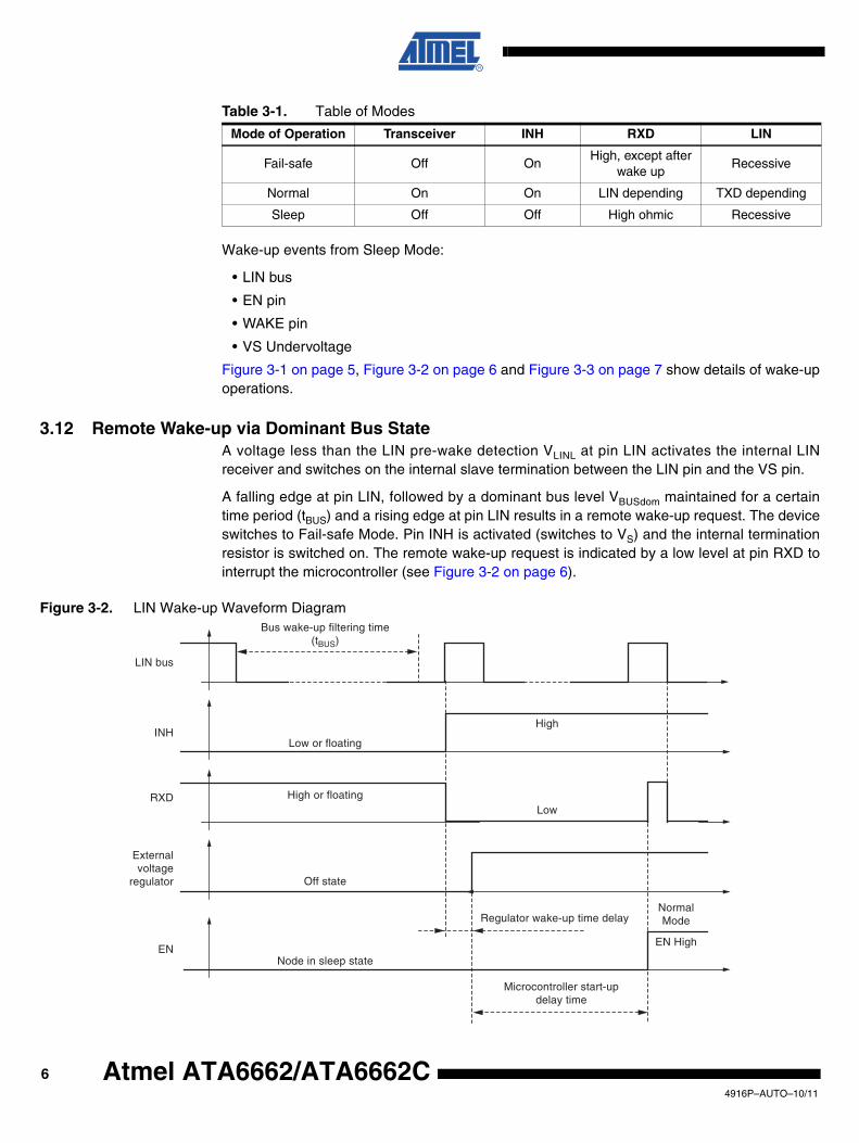
3.12 Remote Wake-up via Dominant Bus StateA voltage less than the LIN pre-wake detection VLINL at pin LIN activates the internal LINreceiver and switches on the internal slave termination between the LIN pin and the VS pin.
A falling edge at pin LIN, followed by a dominant bus level VBUSdom maintained for a certaintime period (tBUS) and a rising edge at pin LIN results in a remote wake-up request. The deviceswitches to Fail-safe Mode. Pin INH is activated (switches to VS) and the internal terminationresistor is switched on. The remote wake-up request is indicated by a low level at pin RXD tointerrupt the microcontroller (see Figure 3-2 on page 6).
Figure 3-2. LIN Wake-up Waveform Diagram
Table 3-1. Table of Modes
Mode of Operation Transceiver INH RXD LIN
Fail-safe Off OnHigh, except after
wake upRecessive
Normal On On LIN depending TXD depending
Sleep Off Off High ohmic Recessive
Microcontroller start-updelay time
Bus wake-up filtering time(tBUS)
Off state
Node in sleep state
High or floating
Low or floating
Low
High
EN High
NormalModeRegulator wake-up time delay
INH
Externalvoltage
regulator
EN
RXD
LIN bus
64916P–AUTO–10/11
Atmel ATA6662/ATA6662C

Atmel ATA6662/ATA6662C
3.13 Local Wake-up via Pin WAKEA falling edge at pin WAKE, followed by a low level maintained for a certain time period(tWAKE), results in a local wake-up request. The wake-up time (tWAKE) ensures that no transient,according to ISO7637, creates a wake-up. The device switches to Fail-safe Mode. Pin INH isactivated (switches to VS) and the internal termination resistor is switched on. The localwake-up request is indicated by a low level at pin RXD to interrupt the microcontroller and astrong pull-down at pin TXD (see Figure on page 9). The voltage threshold for a wake-up sig-nal is 3V below the VS voltage with an output current of typical –3µA. Even in the case of acontinuous low at pin WAKE it is possible to switch the IC into Sleep Mode via a low at pin EN.The IC will stay in Sleep Mode for an unlimited time. To generate a new wake up at pin WAKEit needs first a high signal > 6µs before a negative edge starts the wake-up filtering time again.
Figure 3-3. Wake-up from Wake-up Switch
Microcontroller start-updelay time
Wake filtering timetWAKE
Off state
Node in sleep state
High or floating
TXD weak pull-down resistor
Low or floating
State change
TXD strong pull-down
Node inoperation
Weakpull-down
EN High
HighLow
On state
High
Regulator wake-up time delay
Wake pin
INH
EN
TXD
RXD
Voltageregulator
74916P–AUTO–10/11

3.14 Wake-up Source RecognitionThe device can distinguish between a local wake-up request (pin WAKE) and a remotewake-up request (LIN bus). The wake-up source can be read on pin TXD in Fail-safe Mode. Ifan external pull-up resistor (typically 5kΩ) has been added on pin TXD to the power supply ofthe microcontroller, a high level indicates a remote wake-up request (weak pull-down at pinTXD) and a low level indicates a local wake-up request (strong pull-down at pin TXD).
The wake-up request flag (signalled on pin RXD) as well as the wake-up source flag (signalledon pin TXD) are reset immediately if the microcontroller sets pin EN to high (see Figure 3-2 onpage 6 and Figure 3-3 on page 7).
3.15 Fail-safe Features• The reverse current is < 2µA at pin LIN during loss of VBAT; this is optimal behavior for bus
systems where some slave nodes are supplied from battery or ignition.
• Pin EN provides a pull-down resistor to force the transceiver into Sleep Mode if EN is disconnected.
• Pin RXD is set floating if VBAT is disconnected.
• Pin TXD provides a pull-down resistor to provide a static low if TXD is disconnected.
• The LIN output driver has a current limitation, and if the junction temperature Tj exceeds the thermal shut-down temperature Toff, the output driver switches off.
• The implemented hysteresis, Thys, enables the LIN output again after the temperature has been decreased.
84916P–AUTO–10/11
Atmel ATA6662/ATA6662C

Atmel ATA6662/ATA6662C
4. Absolute Maximum RatingsStresses beyond those listed under “Absolute Maximum Ratings” may cause permanent damage to the device. This is a stress rating only and functional operation of the device at these or any other conditions beyond those indicated in the operational sections of this specification is not implied. Exposure to absolute maximum rating conditions for extended periods may affect device reliability.
Parameters Symbol Min. Typ. Max. Unit
VS- Continuous supply voltage
–0.3 +40 V
Wake DC and transient voltage (with 33-kΩ serial resistor)- Transient voltage due to ISO7637 (coupling 1 nF)
–1–150
+40+100
VV
Logic pins (RXD, TXD, EN) –0.3 +5.5 V
LIN- DC voltage- Transient voltage due to ISO7637 (coupling 1nF)
–27–150
+40+100
VV
INH- DC voltage –0.3 VS + 0.3 V
ESD according to IBEE LIN EMCTest specification 1.0 following IEC 61000-4-2
- Pin VS, LIN to GND- Pin WAKE (33kΩ serial resistor)
±6±5
KVKV
ESD HBM following STM5.1with 1.5kΩ/100pF
- Pin VS, LIN, WAKE, INH to GND ±6 KV
HBM ESDANSI/ESD-STM5.1JESD22-A114AEC-Q100 (002)
±3 KV
CDM ESD STM 5.3.1 ±750 V
Machine Model ESDAEC-Q100-RevF(003)
±100 V
Junction temperature Tj –40 +150 °C
Storage temperature Tstg –55 +150 °C
5. Thermal CharacteristicsParameters Symbol Min. Typ. Max. Unit
Thermal resistance junction ambient RthJA 145 K/W
Special heat sink at GND (pin 5) on PCB (fused lead frame to pin 5)
RthJA 80 K/W
Thermal shutdown Toff 150 165 180 °C
Thermal shutdown hysteresis Thys 5 10 20 °C
94916P–AUTO–10/11

6. Electrical Characteristics5V < VS < 27V, Tj = –40°C to +150°C
No. Parameters Test Conditions Pin Symbol Min. Typ. Max. Unit Type*
1 VS Pin
1.1 DC voltage range nominal 7 VS 5 13.5 27 V A
1.2 Supply current in Sleep ModeSleep ModeVLIN > VS – 0.5VVS < 14V
7 IVSsleep 10 20 µA A
1.3
Supply current in Normal Mode
Bus recessiveVS < 14V
7 IVSrec 0.9 1.3 mA A
1.4Bus dominantVS < 14VTotal bus load > 500Ω
7 IVSdom 1.2 2 mA A
1.5 Supply current in Fail-safe ModeBus recessiveVS < 14V
7 IVSfail 0.5 1.1 mA A
1.6 VS undervoltage threshold on VSth 4 4.95 V A
1.7 VS undervoltage threshold off VSth 4.05 5 V A
1.8VS undervoltage threshold hysteresis
7 VSth_hys 50 500 mV A
2 RXD Output Pin (Open Drain)
2.1 Low-level output sink currentNormal ModeVLIN = 0V, VRXD = 0.4V
1 IRXDL 1.3 2.5 8 mA A
2.2 RXD saturation voltage 5-kΩ pull-up resistor to 5V 1 VsatRXD 0.4 V A
2.3 High-level leakage currentNormal ModeVLIN = VBAT, VRXD = 5V
1 IRXDH –3 +3 µA A
2.4 ESD zener diode IRXD = 100µA 1 VZRXD 5.8 8.6 V A
3 TXD Input Pin
3.1 Low-level voltage input 4 VTXDL –0.3 +0.8 V A
3.2 High-level voltage input 4 VTXDH 2 5.5 V A
3.3 Pull-down resistor VTXD = 5V 4 RTXD 125 250 600 kΩ A
3.4 Low-level leakage current VTXD = 0V 4 ITXD_leak –3 +3 µA A
3.5 Low-level output sink currentFail-safe Mode, local wake upVTXD = 0.4VVLIN = VBAT
4 ITXD 1.3 2.5 8 mA A
4 EN Input Pin
4.1 Low-level voltage input 2 VENL –0.3 +0.8 V A
4.2 High-level voltage input 2 VENH 2 5.5 V A
4.3 Pull-down resistor VEN = 5V 2 REN 125 250 600 kΩ A
4.4 Low-level input current VEN = 0V 2 IEN –3 +3 µA A
5 INH Output Pin
5.1 High-level voltageNormal ModeIINH = –2mA
8 VINHH VS – 3 VS V A
5.2 Leakage currentSleep ModeVINH = 0V/27V, VS = 27V
8 IINHL –3 +3 µA A
*) Type means: A = 100% tested, B = 100% correlation tested, C = Characterized on samples, D = Design parameter
104916P–AUTO–10/11
Atmel ATA6662/ATA6662C

Atmel ATA6662/ATA6662C
6 WAKE Pin
6.1 High-level input voltage 3 VWAKEHVS – 1V
VS + 0.3V
V A
6.2 Low-level input voltage IWAKE = Typically –3µA 3 VWAKEL –1VVS – 3.3V
V A
6.3 Wake pull-up current VS < 27V 3 IWAKE –30 –10 µA A
6.4 High-level leakage current VS = 27V, VWAKE = 27V 3 IWAKE –5 +5 µA A
7 LIN Bus Driver
7.1 Driver recessive output voltage RLOAD = 500Ω / 1kΩ 6 VBUSrec0.9 ×
VSVS V A
7.2Driver dominant voltageVBUSdom_DRV_LoSUP
VVS = 7V, Rload = 500Ω 6 V_LoSUP 1.2 V A
7.3Driver dominant voltageVBUSdom_DRV_HiSUP
VVS = 18V, Rload = 500Ω 6 V_HiSUP 2 V A
7.4Driver dominant voltageVBUSdom_DRV_LoSUP
VVS = 7V, Rload = 1000Ω 6 V_LoSUP_1k 0.6 V A
7.5Driver dominant voltageVBUSdom_DRV_HiSUP
VVS = 18V, Rload = 1000Ω 6 V_HiSUP_1k_ 0.8 V A
7.6 Pull-up resistor to VS The serial diode is mandatory 6 RLIN 20 30 60 kΩ A
7.7 Voltage drop at the serial diodesIn pull-up path with RslaveISerDiode = 10mA
6 VSerDiode 0.4 1.0 V D
7.8LIN current limitationVBUS = VBAT_max
6 IBUS_LIM 40 120 200 mA A
7.9Input leakage current at the receiver, including pull-up resistor as specified
Input leakage currentDriver offVBUS = 0V, VS = 12V
6 IBUS_PAS_dom –1 mA A
7.10 Leakage current LIN recessive
Driver off8V < VBAT < 18V8V < VBUS < 18VVBUS ≥ VBAT
6 IBUS_PAS_rec 10 20 µA A
7.11
Leakage current at ground loss; Control unit disconnected from ground; Loss of local ground must not affected communication in the residual network
GNDDevice = VSVBAT =12V0V < VBUS < 18V
6 IBUS_NO_gnd –10 +0.5 +10 µA A
7.12
Leakage current at loss of battery; Node has to substain the current that can flow under this condition; Bus must remain operational under this condition
VBAT disconnected VSUP_Device = GND0V < VBUS < 18V
6 IBUS_NO_bat 0.1 2 µA A
7.13 Capacitance on pin LIN to GND 6 CLIN 20 pF D
6. Electrical Characteristics (Continued)5V < VS < 27V, Tj = –40°C to +150°C
No. Parameters Test Conditions Pin Symbol Min. Typ. Max. Unit Type*
*) Type means: A = 100% tested, B = 100% correlation tested, C = Characterized on samples, D = Design parameter
114916P–AUTO–10/11

8 LIN Bus Receiver
8.1 Center of receiver thresholdVBUS_CNT = (Vth_dom + Vth_rec) / 2
6 VBUS_CNT0.475 ×
VS
0.5 × VS
0.525 × VS
V A
8.2 Receiver dominant state VEN = 5V 6 VBUSdom –270.4 ×
VSV A
8.3 Receiver recessive state VEN = 5V 6 VBUSrec0.6 ×
VS40 V A
8.4 Receiver input hysteresis VHYS = Vth_rec – Vth_dom 6 VBUShys0.028 ×
VS
0.1 × VS
0.175 × VS
V A
8.5Pre-wake detection LINHigh-level input voltage
6 VLINHVS – 2V
VS + 0.3V
V A
8.6Pre-wake detection LINLow-level input voltage
Switches the LIN receiver on 6 VLINL –27VVS – 3.3V
V A
9 Internal Timers
9.1Dominant time for wake-up via LIN bus
VLIN = 0V 6 tBUS 30 90 150 µs A
9.2Time of low pulse for wake-up via pin WAKE
VWAKE = 0V 3 tWAKE 7 35 50 µs A
9.3Time delay for mode change from Fail-safe Mode to Normal Mode via pin EN
VEN = 5V 2 tnorm 2 7 15 µs A
9.4Time delay for mode change from Normal Mode into Sleep Mode via pin EN
VEN = 0V 2 tsleep 2 7 12 µs A
9.5 TXD dominant time out time VTXD = 0V 4 tdom 6 9 20 ms A
9.6Power-up delay between VS = 5V until INH switches to high
VVS = 5V tVS 200 µs A
10
LIN Bus Driver AC Parameter with Different Bus LoadsLoad 1 (small): 1nF, 1kΩ ; Load 2 (large): 10nF, 500Ω ; RRXD = 5kΩ ; CRXD = 20pF;Load 3 (medium): 6.8nF, 660Ω characterized on samples; 10.1 and 10.2 specifies the timing parameters for properoperation at 20Kbit/s, 10.3 and 10.4 at 10.4Kbit/s.
10.1 Duty cycle 1
THRec(max) = 0.744 × VSTHDom(max) = 0.581 × VSVS = 7.0V to 18VtBit = 50µsD1 = tbus_rec(min) / (2 × tBit)
6 D1 0.396 A
10.2 Duty cycle 2
THRec(min) = 0.422 × VSTHDom(min) = 0.284 × VSVS = 7.0V to 18VtBit = 50µsD2 = tbus_rec(max) / (2 × tBit)
6 D2 0.581 A
10.3 Duty cycle 3
THRec(max) = 0.778 × VSTHDom(max) = 0.616 × VSVS = 7.0V to 18VtBit = 96µsD3 = tbus_rec(min) / (2 × tBit)
6 D3 0.417 A
6. Electrical Characteristics (Continued)5V < VS < 27V, Tj = –40°C to +150°C
No. Parameters Test Conditions Pin Symbol Min. Typ. Max. Unit Type*
*) Type means: A = 100% tested, B = 100% correlation tested, C = Characterized on samples, D = Design parameter
124916P–AUTO–10/11
Atmel ATA6662/ATA6662C

Atmel ATA6662/ATA6662C
Figure 6-1. Definition of Bus Timing Parameter
10.4 Duty cycle 4
THRec(min) = 0.389 × VSTHDom(min) = 0.251 × VSVS = 7.0V to 18VtBit = 96µsD4 = tbus_rec(max) / (2 × tBit)
6 D4 0.590 A
11Receiver Electrical AC Parameters of the LIN Physical LayerLIN receiver, RXD load conditions: CRXD = 20pF, Rpull-up = 5kΩ
11.1Propagation delay of receiver (see Figure 6-1 on page 13)
trec_pd = max(trx_pdr, trx_pdf)VS = 7.0V to 18V
1 trx_pd 6 µs A
11.2Symmetry of receiver propagation delay rising edge minus falling edge
trx_sym = trx_pdr – trx_pdfVS = 7.0V to 18V
1 trx_sym –2 +2 µs A
6. Electrical Characteristics (Continued)5V < VS < 27V, Tj = –40°C to +150°C
No. Parameters Test Conditions Pin Symbol Min. Typ. Max. Unit Type*
*) Type means: A = 100% tested, B = 100% correlation tested, C = Characterized on samples, D = Design parameter
VS(Transceiver supply of transmitting node)
TXD (Input to transmitting node)
RXD(Output of receiving node 1)
LIN Bus Signal
tBit
tBus_dom(max)
tBus_dom(min)
tBus_rec(min)
tBus_rec(max)
RXD(Output of receiving node 2)
THRec(max)
THDom(max)
THDom(min)
THRec(min)
Thresholds of
receiving node 1
Thresholds of
receiving node 2
trx_pdf(1) trx_pdr(1)
trx_pdr(2) trx_pdf(2)
tBit tBit
134916P–AUTO–10/11

Figure 6-2. Application Circuit
VSVS
INH
8
EN
2
RXD
12V
5V
VBATTERY
5 kΩ
1k100 nF
ATA6662
33 kΩ
10 kΩ
1
Short-circuit andovertemperature
protection
Control unit
Slew rate control
Wake-up bus timer
Filter
Master nodepull-up
Wake-uptimer
TXDTime-out
timer
Sleep mode
Receiver
WAKE
3
TXD
Microcontroller
IO
VDD
Externalswitch
4
5
GND
6
7
VS
LIN
LIN
sub
bus
220 pF
22 µF
GND
144916P–AUTO–10/11
Atmel ATA6662/ATA6662C

Atmel ATA6662/ATA6662C
8. Package Information
7. Ordering InformationExtended Type Number Package Remarks
ATA6662-TAQY SO8 LIN transceiver, Pb-free, 4k, taped and reeled
ATA6662C-TAQY SO8 LIN transceiver, Pb-free, 4k, taped and reeled
Package: SO 8
Dimensions in mm
specificationsaccording to DINtechnical drawings
Issue: 1; 15.08.06
Drawing-No.: 6.541-5031.01-4
1 4
8 5
0.2
5±0.2
3.8±0.1
6±0.2
3.7±0.1
4.9±0.1
3.81
0.4
1.27 0.1+
0.15
1.4
154916P–AUTO–10/11

9. Revision History
Please note that the following page numbers referred to in this section refer to the specific revision mentioned, not to this document.
Revision No. History
4916P-AUTO-10/11 • Section 3.11 “Operation Modes” on page 5 changed
4916O-AUTO-05/10• Features on page 1 changed
• Heading 3.6: text changed
4916N-AUTO-03/10
• Features on page 1 changed• Section 4 “Absolute Maximum Ratings” on page 9 changed
• Section 6 “Electrical Characteristics” number 7.13 on page 11 added
• Section 7 “Ordering Information” on page 16 changed
4916M-AUTO-09/09• Figure 1-1 “Block Diagram” on page 1 changed• Section 4 “Absolute Maximum Ratings” on page 8 changed
• Figure 6-2 “Application Circuit” on page 14 changed
4916L-AUTO-02/09 • Section 6 “El.Characteristics” numbers 3.2 and 4.2 on page 9 changed
4916K-AUTO-12/08
• Figure 2-1 “Pinning SO8” on page 2 changed
• Section 3.2 “Supply Pin (VS)” on page 3 changed• Section 3.8 “Enable Input Pin (EN)” on page 4 changed
• Section 3.11 “Operation Modes” on page 5 changed
• Section 3.12 “Remote Wake-up via Dominant Bus State” on page 5 changed• Section 3.14 “Wake-up Source Recognition” on page 6 changed
• Figure 3.2 “LIN Wake-up Waveform Diagram” on page 7 changed
• Figure 3.3 “Wake-up from Wake-up Switch” on page 7 changed
• Section 4 “Absolute Maximum Ratings” on page 8 changed• Section 5 “Thermal Resistance” on page 8 changed
• Section 6 “Electrical Characteristics” on pages 9 to 12 changed
• Figure 6-2 “Application Circuit” on page 13 changed
4916J-AUTO-02/08
• “Pre-normal Mode” in “Fail-safe Mode” changed• Section 3.9 “Inhibit Output Pin (INH) on page 4 changed
• Section 4 “Absolute Maximum Ratings” on page 8 changed
• Section 6 “Electrical Characteristics” number 5.1 on page 9 changed
4916I-AUTO-12/07• Section 3.1 “Physical Layer Compatibility” on page 3 added• Section 6 “El.Characteristics” numbers 1.5, 1.6 and 1.7 on page 9 changed
4916H-AUTO-10/07 • Section 7 “Ordering Information” on page 14 changed
4916G-AUTO-07/07• Put datasheet in a new template
• Capital T for time generally changed in a lower case t
164916P–AUTO–10/11
Atmel ATA6662/ATA6662C

Atmel ATA6662/ATA6662C
4916F-AUTO-05/07
• Figure 1-1 “Block Diagram” on page 1 changed• Figure 6-2 “Application Circuit” on page 13 changed
• Features on page 1 changed
• Section 6 “El.Characteristics” numbers 10.1 to 10.4 and 11.1, 11.2 changed
4916E-AUTO-02/07• Section 4 “Absolute Maximum Ratings” on page 8 changed• Section 2 “Electrical Characteristics” on pages 9 to 11 changed
4916D-AUTO-02/07
• Features on page 1 changed
• Section 1 “Description” on page 1 changed
• Table 2-1 “Pin Description” on page 2 changed• Section 3.2 “Ground Pin (GND) on page 3 changed
• Section 3.7 “Enable Input Pin (EN)” on page 4 changed
• Section 3.11 “Remote Wake-up via Dominant Bus State” on page 5 changed• Figure 3-1 “Mode of Operation” on page 6 changed
• Section 3-14 “Fail-safe Features” on page 6 changed
• Section 4 “Absolute Maximum Ratings” on page 8 changed• Section 6 “Electrical Characteristics” on pages 9 to 11 changed
Please note that the following page numbers referred to in this section refer to the specific revision mentioned, not to this document. (Continued)
Revision No. History
174916P–AUTO–10/11

Atmel Corporation2325 Orchard ParkwaySan Jose, CA 95131USATel: (+1)(408) 441-0311Fax: (+1)(408) 487-2600
Atmel Asia LimitedUnit 01-5 & 16, 19/FBEA Tower, Millennium City 5418 Kwun Tong RoadKwun Tong, KowloonHONG KONGTel: (+852) 2245-6100Fax: (+852) 2722-1369
Atmel Munich GmbHBusiness CampusParkring 4D-85748 Garching b. MunichGERMANYTel: (+49) 89-31970-0Fax: (+49) 89-3194621
Atmel Japan9F, Tonetsu Shinkawa Bldg.1-24-8 ShinkawaChuo-ku, Tokyo 104-0033JAPANTel: (+81) (3) 3523-3551Fax: (+81) (3) 3523-7581
© 2011 Atmel Corporation. All rights reserved. / Rev.: 4916P–AUTO–10/11
Atmel®, Atmel logo and combinations thereof, and others are registered trademarks or trademarks of Atmel Corporation or its subsidiaries. Other terms and product names may be trademarks of others.
Disclaimer: The information in this document is provided in connection with Atmel products. No license, express or implied, by estoppel or otherwise, to any intellec-tual property right is granted by this document or in connection with the sale of Atmel products. EXCEPT AS SET FORTH IN THE ATMEL TERMS AND CONDITIONSOF SALES LOCATED ON THE ATMEL WEBSITE, ATMEL ASSUMES NO LIABILITY WHATSOEVER AND DISCLAIMS ANY EXPRESS, IMPLIED OR STATUTORYWARRANTY RELATING TO ITS PRODUCTS INCLUDING, BUT NOT LIMITED TO, THE IMPLIED WARRANTY OF MERCHANTABILITY, FITNESS FOR A PARTICU-LAR PURPOSE, OR NON-INFRINGEMENT. IN NO EVENT SHALL ATMEL BE LIABLE FOR ANY DIRECT, INDIRECT, CONSEQUENTIAL, PUNITIVE, SPECIAL ORINCIDENTAL DAMAGES (INCLUDING, WITHOUT LIMITATION, DAMAGES FOR LOSS AND PROFITS, BUSINESS INTERRUPTION, OR LOSS OF INFORMATION)ARISING OUT OF THE USE OR INABILITY TO USE THIS DOCUMENT, EVEN IF ATMEL HAS BEEN ADVISED OF THE POSSIBILITY OF SUCH DAMAGES. Atmelmakes no representations or warranties with respect to the accuracy or completeness of the contents of this document and reserves the right to make changes tospecifications and products descriptions at any time without notice. Atmel does not make any commitment to update the information contained herein. Unless specif-ically provided otherwise, Atmel products are not suitable for, and shall not be used in, automotive applications. Atmel products are not intended, authorized, or war-ranted for use as components in applications intended to support or sustain life.