light emission and floating gate memory characteristics of germanium nanocrystals
TRANSCRIPT

Phys. Status Solidi A 208, No. 3, 635–638 (2011) / DOI 10.1002/pssa.201000408 p s sa
statu
s
soli
di
www.pss-a.comph
ysi
ca
applications and materials science
Light emission and floating gatememory characteristics of germaniumnanocrystals
Samaresh Das1, Santanu Manna1, Rajkumar Singha1, Aleksei Anopchenko2, Nicola Daldosso2,Lorenzo Pavesi2, Achintya Dhar1, and Samit Kumar Ray*,1
1Department of Physics and Meteorology, Indian Institute of Technology Kharagpur, Kharagpur-721302, India2Laboratorio di Nanoscienze, Dipartimento di Fisica, Universita di Trento, Via Sommarive 14, 38100 Povo (Trento), Italy
Received 7 June 2010, revised 22 November 2010, accepted 19 January 2011
Published online 8 February 2011
Keywords charge injection, electroluminescence, germanium, nanocrystals
*Corresponding author: e-mail [email protected], Phone: þ91 3222 283838, Fax: þ91 3222 255303
We report Ge nanocrystals (NCs) based dual functional light
emitting and metal insulator semiconductor (MIS) flash
memory devices, fabricated by rf sputtering. Transmission
electron micrographs revealed the formation of spherically
shaped Ge NCs. We have observed broad electroluminescence
(EL) around 760 nm, which is attributed to electron–hole
recombination in quantum confined Ge NCs. The dependence
of integrated EL intensity on drive currents has also been
studied. An anti-clockwise hysteresis behaviour is observed in
capacitance–voltage measurements of MIS devices for differ-
ent sweep voltages, indicating net electron trapping inNCbased
floating gates.
� 2011 WILEY-VCH Verlag GmbH & Co. KGaA, Weinheim
1 Introduction Multifunctional electronic devicesare attractive since one device can play a role of two ormore. Light emitting diodes solar cells, light emittingtransistors and light emitting memory devices [1] arerepresentative dual functional devices. Nanocrystal (NC)light emitting memory devices have dual functions of MOSlight emitting diodes and floating gate memory behaviour. InNCs floating gate devices, metal or semiconductor NCs areembedded as charge-storage nodes in an oxide layer betweenthe control gate and the tunnelling layer to replace thecontinuous floating gate layers in conventional flashmemories [1–3]. The use of NCs as floating gates offerssmaller operating voltages, better endurance characteristicsand faster write/erase speeds as compared to conventionalflash memories [4, 5]. Due to the smaller band-gap, superiorcarriermobilities and higher excitonicBohr radius comparedto Si, Ge NCs are considered to be ideal nodes for use incomplementary metal oxide semiconductor compatiblememory circuits. On the other hand, persistent efforts havebeen made to achieve efficient light emission from silicon–germanium NCs, in order to extend the use of silicontechnology into fully integrated optoelectronic circuits,meeting the requirements for high-bandwidth intrachip andinterchip connects [6]. Light emission in bulk silicon-based
devices is constrained inwavelength to infrared region and inefficiency by the indirect bandgap of silicon. Enhanced lightemission from silicon is predicted to be theoretically possible[7], enabledmostly through quantum-confinement effects [8,9]. There are only few reports onGeNCs basedLED [10, 11].One of the main problems of LED based on Ge NCs in oxidematrix is the carrier injection. The light emission from theseMOS devices is explained by (i) impact ionization of NCs byhot electron injection into the oxide matrix under a high-electric field or (ii) co-tunnelling of carriers into NCs fromboth side of the devices.
In this paper, we report the fabrication of Ge NCs dualfunctional light emittingmetal insulator semiconductor (MIS)based flashmemory devices by rf sputtering.We have studiedthe light emission and charge trapping behaviour of Al/HfO2/HfO2þGe-NCs/HfO2/Si MIS structure. Observed polaritydependent light emission in the electroluminescence (EL)measurements is attributed to the co-tunnelling of electronsand holes into the NCs embedded in HfO2 matrix rather thanimpact ionization. An anti-clockwise hysteresis behaviour isobserved in capacitance–voltage (C–V) measurements fordifferent sweep voltages, indicating net electron trapping inNCs. By using a high-k dielectric in place of SiO2, a largertunnelling current is achieved in MIS LEDs due to the lower
� 2011 WILEY-VCH Verlag GmbH & Co. KGaA, Weinheim
636 S. Das et al.: Light emission and floating gate memory characteristics of Ge nanocrystalsp
hys
ica ssp st
atu
s
solid
i a
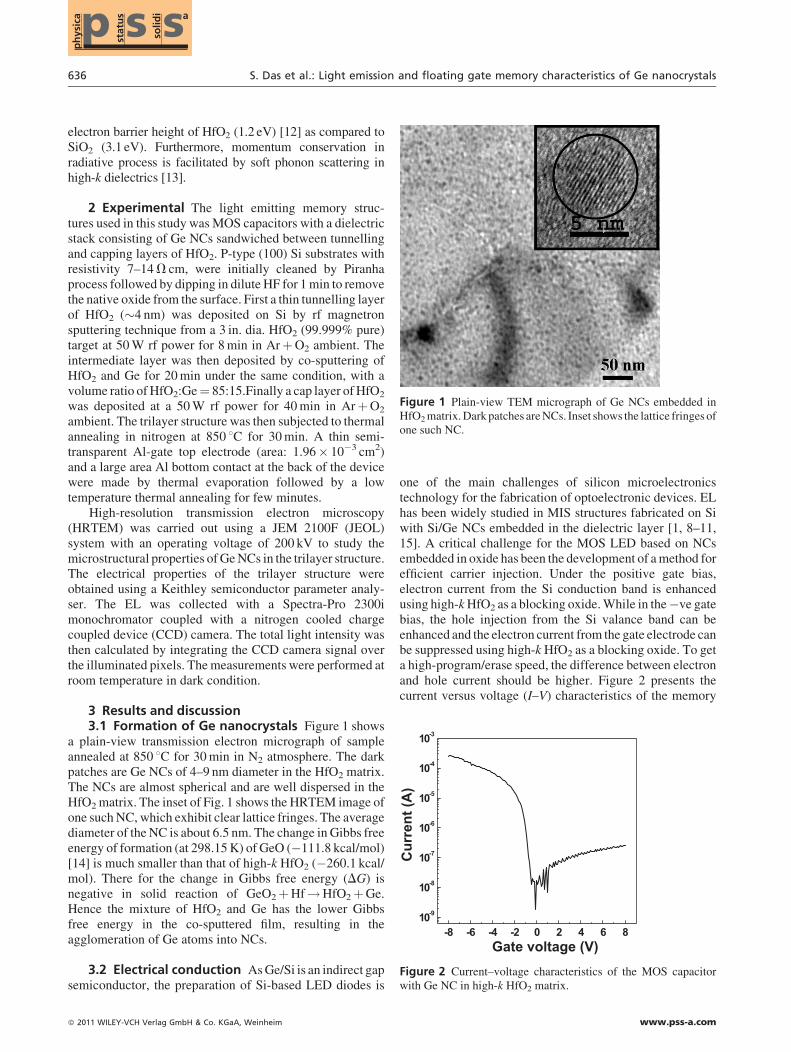
Figure 1 Plain-view TEM micrograph of Ge NCs embedded inHfO2matrix.Darkpatches areNCs. Inset shows the lattice fringes ofone such NC.
-8 -6 -4 -2 0 2 4 6 810-9
10-8
10-7
10-6
10-5
10-4
10-3
Cur
rent
(A)
Gate voltage (V)Figure 2 Current–voltage characteristics of the MOS capacitorwith Ge NC in high-k HfO2 matrix.
electron barrier height of HfO2 (1.2 eV) [12] as compared toSiO2 (3.1 eV). Furthermore, momentum conservation inradiative process is facilitated by soft phonon scattering inhigh-k dielectrics [13].
2 Experimental The light emitting memory struc-tures used in this study was MOS capacitors with a dielectricstack consisting of Ge NCs sandwiched between tunnellingand capping layers of HfO2. P-type (100) Si substrates withresistivity 7–14V cm, were initially cleaned by Piranhaprocess followed by dipping in dilute HF for 1min to removethe native oxide from the surface. First a thin tunnelling layerof HfO2 (�4 nm) was deposited on Si by rf magnetronsputtering technique from a 3 in. dia. HfO2 (99.999% pure)target at 50W rf power for 8min in ArþO2 ambient. Theintermediate layer was then deposited by co-sputtering ofHfO2 and Ge for 20min under the same condition, with avolume ratio ofHfO2:Ge¼ 85:15.Finally a cap layer ofHfO2
was deposited at a 50W rf power for 40min in ArþO2
ambient. The trilayer structure was then subjected to thermalannealing in nitrogen at 850 8C for 30min. A thin semi-transparent Al-gate top electrode (area: 1.96� 10�3 cm2)and a large area Al bottom contact at the back of the devicewere made by thermal evaporation followed by a lowtemperature thermal annealing for few minutes.
High-resolution transmission electron microscopy(HRTEM) was carried out using a JEM 2100F (JEOL)system with an operating voltage of 200 kV to study themicrostructural properties ofGeNCs in the trilayer structure.The electrical properties of the trilayer structure wereobtained using a Keithley semiconductor parameter analy-ser. The EL was collected with a Spectra-Pro 2300imonochromator coupled with a nitrogen cooled chargecoupled device (CCD) camera. The total light intensity wasthen calculated by integrating the CCD camera signal overthe illuminated pixels. Themeasurements were performed atroom temperature in dark condition.
3 Results and discussion3.1 Formation of Ge nanocrystals Figure 1 shows
a plain-view transmission electron micrograph of sampleannealed at 850 8C for 30min in N2 atmosphere. The darkpatches are Ge NCs of 4–9 nm diameter in the HfO2 matrix.The NCs are almost spherical and are well dispersed in theHfO2matrix. The inset of Fig. 1 shows the HRTEM image ofone suchNC, which exhibit clear lattice fringes. The averagediameter of the NC is about 6.5 nm. The change in Gibbs freeenergy of formation (at 298.15K) of GeO (�111.8 kcal/mol)[14] is much smaller than that of high-k HfO2 (�260.1 kcal/mol). There for the change in Gibbs free energy (DG) isnegative in solid reaction of GeO2þHf!HfO2þGe.Hence the mixture of HfO2 and Ge has the lower Gibbsfree energy in the co-sputtered film, resulting in theagglomeration of Ge atoms into NCs.
3.2 Electrical conduction AsGe/Si is an indirect gapsemiconductor, the preparation of Si-based LED diodes is
� 2011 WILEY-VCH Verlag GmbH & Co. KGaA, Weinheim
one of the main challenges of silicon microelectronicstechnology for the fabrication of optoelectronic devices. ELhas been widely studied in MIS structures fabricated on Siwith Si/Ge NCs embedded in the dielectric layer [1, 8–11,15]. A critical challenge for the MOS LED based on NCsembedded in oxide has been the development of amethod forefficient carrier injection. Under the positive gate bias,electron current from the Si conduction band is enhancedusing high-kHfO2 as a blocking oxide.While in the�ve gatebias, the hole injection from the Si valance band can beenhanced and the electron current from the gate electrode canbe suppressed using high-kHfO2 as a blocking oxide. To geta high-program/erase speed, the difference between electronand hole current should be higher. Figure 2 presents thecurrent versus voltage (I–V) characteristics of the memory
www.pss-a.com

Phys. Status Solidi A 208, No. 3 (2011) 637
Original
Paper
500 600 700 800 900 1000
EL In
tens
ity (a
rb. u
nits
)
Wavelength (nm)
at 9.8 mA at 15 mA at 18 mA
Figure 4 EL spectra at the injected currents of 9.8, 15 and 18mA.The spectra are normalized for spectrograph response.
structure. The tunnelling effect owing to NCs is clearly seenin both accumulation and inversion, when the I–V curvebends over in the intermediate voltage region and the currentincreases slowly for voltages up to 8V. The detailedtunnelling mechanisms through high-dielectric permittivitymaterials are still under investigation. Fowler–Nordheim(F–N) tunnelling, direct tunnelling and Frenkel–Pooletunnelling (F–P) have been proposed to explain theexperimental results at various voltage ranges [12, 16]. It isalso well known that the F–N tunnelling current is higher,when it is due to themajority carriers and relatively weak if itis due to the minority carriers. In our device we have alsoseen that for higher electric field the tunnelling current in theaccumulation regime (majority carrier) is higher than that ofinversion regime (minority carrier). It may be noted that alow backward tunnelling current, thin tunnelling oxide andsmall valence band offset between the trapping layer and Sisubstrate are necessary for easy erasing of stored chargesfrom the floating gate. During this erase mode, a negativevoltage is applied at the gate. A small valence band offsetbetween the trapping layer and p-Si enhances the holetunnelling [17], which would recombine with the storedelectrons within the NCs for the erase operation.
3.3 Electroluminescence behaviour The MOSstructure containing Ge NCs embedded in HfO2 shows ELat room temperature. The EL spectra are dependent on thepolarity of the potential bias and emissionwas observed onlyunder negative gate bias. Figure 3 shows the integrated EL(IEL) from the device as a function of current density (J). Thecurve is plotted in double-logarithmic scale. The EL onsetvoltage of the device is about �13V. The IEL� Jcharacteristics posses a power law, i.e. IEL� Ja, with abeing 0.97. This indicates a nearly linear dependence of ELintensity on injection current. The EL spectra collected at theinjected currents of 9.8, 15 and 18mA are shown in Fig. 4.The spectra show a broad EL in the visible and near infraredregion. The EL peak (18mA) can be deconvoluted by threeGaussian peaks with peak position centred at 644, 760 and898 nm with FWHM of 85, 113 and 79 nm, respectively.
10-4 10-3102
103
(b)
EL In
tens
ity (a
rb. u
nits
)
Gate Current (A)Figure 3 IntegratedELintensityasa functionof the injectedcurrent.
www.pss-a.com
Using simple confinement model [2], the 760 nm EL peakscorresponds to 6.9 nm Ge particle size, which closelymatches with the observed one obtained from the TEMmicrograph. Therefore the intense EL peaks at 760 nm can beattributed to electron–hole recombination in the Ge NCs. Onthe other hand, 644 nm emission is far away from thequantum confined effect of 6.5 nmGeNCs. There are severalreports of luminescence in the blue–green region with thepeak energy independent of the size of the NCs [18].Therefore the observed emission band around 644 nmoriginates due to radiative recombination through defects,which are located at the interface of the NCs. Another weakeEL peaks at 898 nm is attributed to the oxygen related defectsin GeO2. It may be noted that, the EL is observed only forforward bias condition with negative voltage at the metalgate. Therefore the observed emission is attributed to theradiative recombination of tunnelled electrons from gateelectrode and holes from p-type Si into the Ge NCs locatedinside the HfO2 matrix rather than the impact ionization thatmight take place in the NCs.
3 . 4 Cha rge in j e c t i on and re t en t i oncharacteristics C–V measurement of memory capacitorshas been an attractive method of obtaining device charac-teristics due to the ease of experimental setup and dataanalysis. Figure 5 shows the high-frequency (1MHz) C–Vcurves for the samplewithGeNCs embedded inHfO2matrixfor different sweep voltages. An anti-clockwise hysteresischaracteristics is observed for the Ge NC try-layer deviceindicating net electron trapping in the Ge-NCs embeddedsandwich structure. A very small flat-band voltage shift of0.13V is observed for the control sample without Ge NCs.This suggests that the origin of C–V hysteresis can beattributed to injected charges mainly in NCs or at theinterfaces between the NCs and the surrounding oxides,rather than the traps in HfO2. For�7V sweep voltage a flat-band voltage shift of 4.85V for NC-MOS devices give riseto a stored charge density (Ncharge) of 1.07� 1013 cm�2
� 2011 WILEY-VCH Verlag GmbH & Co. KGaA, Weinheim

638 S. Das et al.: Light emission and floating gate memory characteristics of Ge nanocrystalsp
hys
ica ssp st
atu
s
solid
i a
-8 -6 -4 -2 0 2 4 6 80.3
0.4
0.5
0.6
0.7
0.8
0.9
1.0
1.1
Nor
mal
ized
cap
acita
nce
Gate voltage (V)
+- 4 V +- 5 V +- 6 V +- 7 V +- 8 V +- 9 V +- 10 V
Figure 5 (online colour at: www.pss-a.com) High-frequency(1MHz) C–V characteristics of MOS capacitor with Ge NCs inhigh-k HfO2 matrix for different sweep voltages.
using [19]
V FB (V
)
Figu
� 20
Ncharge ¼DVFB
qe0
tCOeCO
þ tNCeNC
� � ; (1)
where DVFB is the flat-band voltage shift, q the magnitude ofthe electronic charge; tCO and eCO are the thickness andrelative permittivity of the control oxide; tNC and eNC are thediameter and relative permittivity of the NC; and e0 is thepermittivity of the free space.
Figure 6 shows the charge retention characteristics of theGe NCs nonvolatile memory capacitor. At first, the memorycapacitorwas programmed under a drive gate voltage ofþ7Vfor 1 s. Then, the VFB was measured with time. Similarly, thememory capacitor was erased under a drive gate voltage of�7V for 1 s and the VFB was measured with time. Assuminglogarithmic behaviour for retention, the extrapolation of VFB
shift for memory capacitor has been performed up to 10 years.The memory windows of the device estimated to be 3.03V at
100 101 102 103 104 105 106 107 108 109-5
-4
-3
-2
-1
0
1
2
3.03 V
10 years
Retention time (s)
Program: +7 V, 1 s Erase: -7 V, 1 s
re 6 Retention characteristics of the Ge NCsmemory device.
11 WILEY-VCH Verlag GmbH & Co. KGaA, Weinheim
25 8C after 10 years of retention with charge losses of thememory is estimated to be 37%. Due to the large memorywindow and low charge loss of the Ge NCs memory devicewith high-k HfO2 as a blocking oxide and a high-workfunction metal gate, it can be used in future high-density andscaled flash memory device applications.
4 Conclusions We have demonstrated the light emis-sion and charge trapping behaviour of Al/HfO2/Ge-NCs/HfO2/Si MIS structures. Observed broad EL around 760 nmis attributed to the electron–hole recombination in quantumconfined Ge NCs. An anti-clockwise hysteresis behaviour isobserved in C–Vmeasurements of MIS devices for differentsweep voltages, indicating net electron trapping in NC basedfloating gates.
Acknowledgements This work was supported by DSTITPAR project.
References
[1] R. J. Walters, Nature Mater. 4, 143 (2005).[2] S. Das, K. Das, R. K. Singha, A. Dhar, and S. K. Ray, Appl.
Phys. Lett. 91, 233118 (2007).[3] D. Panda, A. Dhar, and S. K. Ray, Semicond. Sci. Technol.
24, 115020 (2009).[4] D. W. Kim, T. Kim, and S. K. Banerjee, IEEE Trans.
Electron. Devices 50, 1823 (2003).[5] J. Blauwe, IEEE Trans. Nanotechnol. 1, 72 (2002).[6] M. Salib, M. Morse, L. Liao, R. Jones, D. Samara-Rubio, A.
Liu, A. Alduino, and M. Paniccia, Intel. Technol. J. 8, 143(2004).
[7] T. Trupke, M. A. Green, and P. Wurfel, J. Appl. Phys. 93,9058 (2003).
[8] L. Pavesi, L. Dal Negro, C. Mazzoleni, G. Franzo, and F.Priolo, Nature 408, 440 (2000).
[9] M. A. Green, J. Zhao, A. Wang, P. J. Reece, and M. Gal,Nature 412, 805 (2001).
[10] J.-Y. Zhang, Y.-H. Ye, and X.-L. Tan, Appl. Phys. Lett. 74,2459 (1999).
[11] S.-T. Chang, W. C. Wang, and W. K. Lin, Thin Solid Films517, 5070 (2009).
[12] W. J. Zhu, T.-P. Ma, T. Tamagawa, J. Kim, and Y. Di, IEEEElectron Device Lett. 23, 97 (2002).
[13] M. V. Fischetti, D. A. Neumayer, and E. A. Cartier, J. Appl.Phys. 90, 4587 (2001).
[14] Aready-Reference Book of Chemical and Physical Data, 70thed., edited by R. C. Weast, D. R. Lide, M. J. Astle, W. H.Beyer (CRC, Boca Raton, Florida, 1990).
[15] A. Marconi, A. Anopchenko, M. Wang, G. Pucker, P. Bel-lutti, and L. Pavesi, Appl. Phys. Lett. 94, 221110 (2009).
[16] H.W. Chen, F. C. Chiu, C. H. Liu, S. Y. Chen, H. S. Huang, P.C. Juan, and H. L. Hwang, Appl. Surf. Sci. 254, 6112 (2008).
[17] S. Maikap, H. Y. Lee, T.-Y. Wang, P.-J. Tzeng, C. C. Wang,L. S. Lee, K. C. Liu, J.-R. Yang, and M.-J. Tsai, Semicond.Sci. Technol. 22, 88 (2007).
[18] J.-Y. Zhang, Y.-H. Ye, X.-L. Tan, and X.-M. Bao, Appl.Phys. A 71, 299 (2000).
[19] T. Hori, T. Ohzone, Y. Odark, and J. Hirase, IEEE IEDMTech. Dig. 92, 469 (1992).
www.pss-a.com