lg 32lc2r
TRANSCRIPT

7/22/2019 lg 32LC2R
http://slidepdf.com/reader/full/lg-32lc2r 1/40
R
LCD TV
SERVICE MANUAL
CAUTIONBEFORE SERVICING THE CHASSIS,
READ THE SAFETY PRECAUTIONS IN THIS MANUAL.
CHASSIS : LP61AFACTORY MODEL : 26LC2R-ZJ / 32LC2R-ZJ
MODEL : 26LC2R / 32LC2R
website:http://biz.LGservice.come-mail:http://www.LGEservice.com/techsup.html

7/22/2019 lg 32LC2R
http://slidepdf.com/reader/full/lg-32lc2r 2/40
- 2 -
CONTENTS
CONTENTS .............................................................................................. 2
SAFETY PRECAUTIONS ..........................................................................3
SPECIFICATION........................................................................................6
ADJUSTMENT INSTRUCTION .................................................................9
TROUBLE SHOOTING............................................................................19
BLOCK DIAGRAM...................................................................................22
EXPLODED VIEW .................................................................................. 24
REPLACEMENT PARTS LIST ............................................................... 28
SVC. SHEET ...............................................................................................

7/22/2019 lg 32LC2R
http://slidepdf.com/reader/full/lg-32lc2r 3/40
- 3 -
SAFETY PRECAUTIONS
Many electrical and mechanical parts in this chassis have special safety-related characteristics. These parts are identified by in the
Schematic Diagram and Replacement Parts List.
It is essential that these special safety parts should be replaced with the same components as recommended in this manual to prevent
Shock, Fire, or other Hazards.
Do not modify the original design without permission of manufacturer.
General Guidance
An isolation Transformer should always be used during the
servicing of a receiver whose chassis is not isolated from the AC
power line. Use a transformer of adequate power rating as this
protects the technician from accidents resulting in personal injury
from electrical shocks.
It will also protect the receiver and it's components from being
damaged by accidental shorts of the circuitry that may be
inadvertently introduced during the service operation.
If any fuse (or Fusible Resistor) in this TV receiver is blown,replace it with the specified.
When replacing a high wattage resistor (Oxide Metal Film Resistor,
over 1W), keep the resistor 10mm away from PCB.
Keep wires away from high voltage or high temperature parts.
Before returning the receiver to the customer,
always perform an AC leakage current check on the exposed
metallic parts of the cabinet, such as antennas, terminals, etc., to
be sure the set is safe to operate without damage of electrical
shock.
Leakage Current Cold Check(Antenna Cold Check)With the instrument AC plug removed from AC source, connect an
electrical jumper across the two AC plug prongs. Place the AC
switch in the on position, connect one lead of ohm-meter to the AC
plug prongs tied together and touch other ohm-meter lead in turn to
each exposed metallic parts such as antenna terminals, phone
jacks, etc.
If the exposed metallic part has a return path to the chassis, the
measured resistance should be between 1MΩ and 5.2MΩ.
When the exposed metal has no return path to the chassis the
reading must be infinite.
An other abnormality exists that must be corrected before the
receiver is returned to the customer.
Leakage Current Hot Check (See below Figure)
Plug the AC cord directly into the AC outlet.
Do not use a line Isolation Transformer during this check.
Connect 1.5K/10watt resistor in parallel with a 0.15uF capacitor
between a known good earth ground (Water Pipe, Conduit, etc.)
and the exposed metallic parts.
Measure the AC voltage across the resistor using AC voltmeter
with 1000 ohms/volt or more sensitivity.
Reverse plug the AC cord into the AC outlet and repeat AC voltage
measurements for each exposed metallic part. Any voltage
measured must not exceed 0.75 volt RMS which is corresponds to
0.5mA.In case any measurement is out of the limits specified, there is
possibility of shock hazard and the set must be checked and
repaired before it is returned to the customer.
Leakage Current Hot Check circuit
1.5 Kohm/10W
To Instrument's
exposedMETALLIC PARTS
Good Earth Groundsuch as WATER PIPE,CONDUIT etc.
AC Volt-meter
IMPORTANT SAFETY NOTICE
0.15uF

7/22/2019 lg 32LC2R
http://slidepdf.com/reader/full/lg-32lc2r 4/40
- 4 -
CAUTION: Before servicing receivers covered by this service
manual and its supplements and addenda, read and follow the
SAFETY PRECAUTIONS on page 3 of this publication.
NOTE: If unforeseen circumstances create conflict between the
following servicing precautions and any of the safety precautions on
page 3 of this publication, always follow the safety precautions.
Remember: Safety First.
General Servicing Precautions1. Always unplug the receiver AC power cord from the AC power
source before;
a. Removing or reinstalling any component, circuit board
module or any other receiver assembly.
b. Disconnecting or reconnecting any receiver electrical plug or
other electrical connection.
c. Connecting a test substitute in parallel with an electrolytic
capacitor in the receiver.
CAUTION: A wrong part substitution or incorrect polarity
installation of electrolytic capacitors may result in an
explosion hazard.
2. Test high voltage only by measuring it with an appropriate high
voltage meter or other voltage measuring device (DVM,
FETVOM, etc) equipped with a suitable high voltage probe.Do not test high voltage by "drawing an arc".
3. Do not spray chemicals on or near this receiver or any of its
assemblies.
4. Unless specified otherwise in this service manual, clean
electrical contacts only by applying the following mixture to the
contacts with a pipe cleaner, cotton-tipped stick or comparable
non-abrasive applicator; 10% (by volume) Acetone and 90% (by
volume) isopropyl alcohol (90%-99% strength)
CAUTION: This is a flammable mixture.
Unless specified otherwise in this service manual, lubrication of
contacts in not required.
5. Do not defeat any plug/socket B+ voltage interlocks with which
receivers covered by this service manual might be equipped.
6. Do not apply AC power to this instrument and/or any of its
electrical assemblies unless all solid-state device heat sinks are
correctly installed.
7. Always connect the test receiver ground lead to the receiver
chassis ground before connecting the test receiver positive
lead.
Always remove the test receiver ground lead last.
8. Use with this receiver only the test fixtures specified in this
service manual.
CAUTION: Do not connect the test fixture ground strap to any
heat sink in this receiver.
Electrostatically Sensitive (ES) Devices
Some semiconductor (solid-state) devices can be damaged easily
by static electricity. Such components commonly are called
Electrostatically Sensitive (ES) Devices. Examples of typical ESdevices are integrated circuits and some field-effect transistors and
semiconductor "chip" components. The following techniques
should be used to help reduce the incidence of component
damage caused by static by static electricity.
1. Immediately before handling any semiconductor component or
semiconductor-equipped assembly, drain off any electrostatic
charge on your body by touching a known earth ground.
Alternatively, obtain and wear a commercially available
discharging wrist strap device, which should be removed to
prevent potential shock reasons prior to applying power to the
unit under test.
2. After removing an electrical assembly equipped with ES
devices, place the assembly on a conductive surface such as
aluminum foil, to prevent electrostatic charge buildup or
exposure of the assembly.
3. Use only a grounded-tip soldering iron to solder or unsolder ES
devices.
4. Use only an anti-static type solder removal device. Some solder
removal devices not classified as "anti-static" can generateelectrical charges sufficient to damage ES devices.
5. Do not use freon-propelled chemicals. These can generate
electrical charges sufficient to damage ES devices.
6. Do not remove a replacement ES device from its protective
package until immediately before you are ready to install it.
(Most replacement ES devices are packaged with leads
electrically shorted together by conductive foam, aluminum foil
or comparable conductive material).
7. Immediately before removing the protective material from the
leads of a replacement ES device, touch the protective material
to the chassis or circuit assembly into which the device will be
installed.
CAUTION: Be sure no power is applied to the chassis or circuit,
and observe all other safety precautions.
8. Minimize bodily motions when handling unpackagedreplacement ES devices. (Otherwise harmless motion such as
the brushing together of your clothes fabric or the lifting of your
foot from a carpeted floor can generate static electricity
sufficient to damage an ES device.)
General Soldering Guidelines
1. Use a grounded-tip, low-wattage soldering iron and appropriate
tip size and shape that will maintain tip temperature within the
range or 500 F to 600 F.
2. Use an appropriate gauge of RMA resin-core solder composed
of 60 parts tin/40 parts lead.
3. Keep the soldering iron tip clean and well tinned.
4. Thoroughly clean the surfaces to be soldered. Use a mall wire-
bristle (0.5 inch, or 1.25cm) brush with a metal handle.
Do not use freon-propelled spray-on cleaners.
5. Use the following unsoldering technique
a. Allow the soldering iron tip to reach normal temperature.
(500 F to 600 F)
b. Heat the component lead until the solder melts.
c. Quickly draw the melted solder with an anti-static, suction-
type solder removal device or with solder braid.
CAUTION: Work quick ly to avoid overheat ing the
circuitboard printed foil.
6. Use the following soldering technique.
a. Allow the soldering iron tip to reach a normal temperature
(500 F to 600 F)
b. First, hold the soldering iron tip and solder the strand against
the component lead until the solder melts.
c. Quickly move the soldering iron tip to the junction of thecomponent lead and the printed circuit foil, and hold it there
only until the solder flows onto and around both the
component lead and the foil.
CAUTION: Work quickly to avoid overheating the circuit
board printed foil.
d. Closely inspect the solder area and remove any excess or
splashed solder with a small wire-bristle brush.
SERVICING PRECAUTIONS

7/22/2019 lg 32LC2R
http://slidepdf.com/reader/full/lg-32lc2r 5/40
- 5 -
IC Remove/Replacement
Some chassis circuit boards have slotted holes (oblong) through
which the IC leads are inserted and then bent flat against the
circuit foil. When holes are the slotted type, the following technique
should be used to remove and replace the IC. When working with
boards using the familiar round hole, use the standard technique
as outlined in paragraphs 5 and 6 above.
Removal
1. Desolder and straighten each IC lead in one operation by gently
prying up on the lead with the soldering iron tip as the soldermelts.
2. Draw away the melted solder with an anti-static suction-type
solder removal device (or with solder braid) before removing the
IC.
Replacement
1. Carefully insert the replacement IC in the circuit board.
2. Carefully bend each IC lead against the circuit foil pad and
solder it.
3. Clean the soldered areas with a small wire-bristle brush.
(It is not necessary to reapply acrylic coating to the areas).
"Small-Signal" Discrete Transistor
Removal/Replacement
1. Remove the defective transistor by clipping its leads as close as
possible to the component body.2. Bend into a "U" shape the end of each of three leads remaining
on the circuit board.
3. Bend into a "U" shape the replacement transistor leads.
4. Connect the replacement transistor leads to the corresponding
leads extending from the circuit board and crimp the "U" with
long nose pliers to insure metal to metal contact then solder
each connection.
Power Output, Transistor Device
Removal/Replacement
1. Heat and remove all solder from around the transistor leads.
2. Remove the heat sink mounting screw (if so equipped).
3. Carefully remove the transistor from the heat sink of the circuit
board.
4. Insert new transistor in the circuit board.
5. Solder each transistor lead, and clip off excess lead.
6. Replace heat sink.
Diode Removal/Replacement
1. Remove defective diode by clipping its leads as close as
possible to diode body.
2. Bend the two remaining leads perpendicular y to the circuit
board.
3. Observing diode polarity, wrap each lead of the new diode
around the corresponding lead on the circuit board.
4. Securely crimp each connection and solder it.
5. Inspect (on the circuit board copper side) the solder joints of
the two "original" leads. If they are not shiny, reheat them and if
necessary, apply additional solder.Fuse and Conventional Resistor
Removal/Replacement
1. Clip each fuse or resistor lead at top of the circuit board hollow
stake.
2. Securely crimp the leads of replacement component around
notch at stake top.
3. Solder the connections.
CAUTION: Maintain original spacing between the replaced
component and adjacent components and the circuit board to
prevent excessive component temperatures.
Circuit Board Foil Repair
Excessive heat applied to the copper foil of any printed circuit
board will weaken the adhesive that bonds the foil to the circuit
board causing the foil to separate from or "lift-off" the board. The
following guidelines and procedures should be followed whenever
this condition is encountered.
At IC Connections
To repair a defective copper pattern at IC connections use the
following procedure to install a jumper wire on the copper patternside of the circuit board. (Use this technique only on IC
connections).
1. Carefully remove the damaged copper pattern with a sharp
knife. (Remove only as much copper as absolutely necessary).
2. carefully scratch away the solder resist and acrylic coating (if
used) from the end of the remaining copper pattern.
3. Bend a small "U" in one end of a small gauge jumper wire and
carefully crimp it around the IC pin. Solder the IC connection.
4. Route the jumper wire along the path of the out-away copper
pattern and let it overlap the previously scraped end of the good
copper pattern. Solder the overlapped area and clip off any
excess jumper wire.
At Other Connections Use the following technique to repair the defective copper pattern
at connections other than IC Pins. This technique involves the
installation of a jumper wire on the component side of the circuit
board.
1. Remove the defective copper pattern with a sharp knife.
Remove at least 1/4 inch of copper, to ensure that a hazardous
condition will not exist if the jumper wire opens.
2. Trace along the copper pattern from both sides of the pattern
break and locate the nearest component that is directly
connected to the affected copper pattern.
3. Connect insulated 20-gauge jumper wire from the lead of the
nearest component on one side of the pattern break to the lead
of the nearest component on the other side.
Carefully crimp and solder the connections.
CAUTION: Be sure the insulated jumper wire is dressed so the
it does not touch components or sharp edges.

7/22/2019 lg 32LC2R
http://slidepdf.com/reader/full/lg-32lc2r 6/40
- 6 -
1. Application rangeThis specification is applied to LP61A chassis.
2. Requirement for TestTesting for standard of each part must be followed in belowcondition.
(1) Temperature : 25°C±5°C(77±9°F), CST : 40±5(2) Humidity : 65%±10%(3) Power : Standard input voltage (AC 100-240V, 50/60Hz)
*Standard Voltage of each products is marked by models(4) Specification and performance of each parts are followed
each drawing and specif ication by part number inaccordance with BOM.
(5) The receiver must be operated for about 20 minutes priorto the adjustment.
3. Test method
3.1 Performance : LGE TV test method followed3.2 Demanded other specification
Safety : CE, IEC SpecificationEMC : CE, IEC
SPECIFICATIONNOTE : Specifications and others are subject to change without notice for improvement.
4. General Specification(LCD Module)
5. Feature and Function
No Item Specification Remark
1. Display Screen Device 26/32" inch wide Color Display Module LCD2. Aspect Ratio 16:9
3. LCD Module 26/32" TFT WXGA LCD MAKER:AUO/CMO/LPL
4. Operating Environment 1) Temp. : 0 ~ 40 deg LGE SPEC
2) Humidity : 0 ~ 85%
5. Storage Environment 3) Temp. : -20 ~ 60 deg
4) Humidity : 0 ~ 85 %
6. Input Voltage AC100 ~ 240V, 50/60Hz
7. Power Consumption Power on/off : ≤ max 160W (32") Volume: 1/8 volume of sound distortion point
(Green) ≤ max 130W (26")
St-By(Red) : 1.0 W (26",32")
No Item Specification Remark
1. RF Input 1 1 Tuner
(PAL BG/I/DK, SECAM-L)
SCART 1 FULL(CVBS/L/R,1H-RGB/L/R,TV_OUT) Rear
Input/Output 1 HALF(CVBS/L/R,S-VHS,MNT_OUT) Rear
AV Input 2 CVBS/L/R, S-VHS(S-VHS Priority) Rear and Side
Audio Out(R/L) 1 Variable Audio Out Rear
Component Input 1 480i /576i/480p/576p/720p/1080i Rear
RGB Input 1 RGB-PC : Up to WXGA 60Hz Rear
RGB-DTV : 480p/576p/720p/1080i
HDMI Input 1 HDMI-DTV : Rear
480i/576i/480p/576p/720p/1080i
RS-232C 1 Remote Control Rear
IR Input 1 Wired IR Rear

7/22/2019 lg 32LC2R
http://slidepdf.com/reader/full/lg-32lc2r 7/40
7/22/2019 lg 32LC2R
http://slidepdf.com/reader/full/lg-32lc2r 8/40
- 8 -
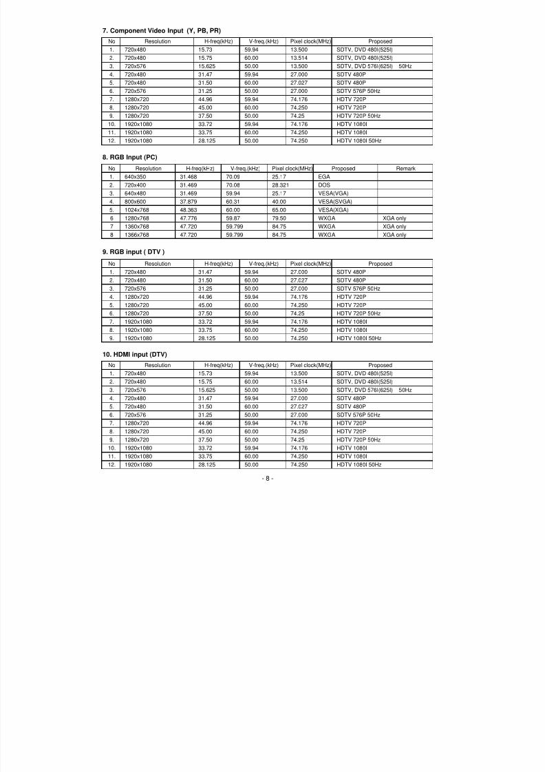
9. RGB input ( DTV )
No Resolution H-freq(kHz) V-freq.(kHz) Pixel clock(MHz) Proposed
1. 720x480 31.47 59.94 27.000 SDTV 480P
2. 720x480 31.50 60.00 27.027 SDTV 480P
3. 720x576 31.25 50.00 27.000 SDTV 576P 50Hz
4. 1280x720 44.96 59.94 74.176 HDTV 720P5. 1280x720 45.00 60.00 74.250 HDTV 720P
6. 1280x720 37.50 50.00 74.25 HDTV 720P 50Hz
7. 1920x1080 33.72 59.94 74.176 HDTV 1080I
8. 1920x1080 33.75 60.00 74.250 HDTV 1080I
9. 1920x1080 28.125 50.00 74.250 HDTV 1080I 50Hz
10. HDMI input (DTV)
No Resolution H-freq(kHz) V-freq.(kHz) Pixel clock(MHz) Proposed
1. 720x480 15.73 59.94 13.500 SDTV, DVD 480I(525I)
2. 720x480 15.75 60.00 13.514 SDTV, DVD 480I(525I)
3. 720x576 15.625 50.00 13.500 SDTV, DVD 576I(625I) 50Hz
4. 720x480 31.47 59.94 27.000 SDTV 480P
5. 720x480 31.50 60.00 27.027 SDTV 480P
6. 720x576 31.25 50.00 27.000 SDTV 576P 50Hz
7. 1280x720 44.96 59.94 74.176 HDTV 720P
8. 1280x720 45.00 60.00 74.250 HDTV 720P
9. 1280x720 37.50 50.00 74.25 HDTV 720P 50Hz
10. 1920x1080 33.72 59.94 74.176 HDTV 1080I
11. 1920x1080 33.75 60.00 74.250 HDTV 1080I
12. 1920x1080 28.125 50.00 74.250 HDTV 1080I 50Hz
7. Component Video Input (Y, PB, PR)
8. RGB Input (PC)
No Resolution H-freq(kHz) V-freq.(kHz) Pixel clock(MHz) Proposed
1. 720x480 15.73 59.94 13.500 SDTV, DVD 480I(525I)
2. 720x480 15.75 60.00 13.514 SDTV, DVD 480I(525I)
3. 720x576 15.625 50.00 13.500 SDTV, DVD 576I(625I) 50Hz
4. 720x480 31.47 59.94 27.000 SDTV 480P
5. 720x480 31.50 60.00 27.027 SDTV 480P
6. 720x576 31.25 50.00 27.000 SDTV 576P 50Hz
7. 1280x720 44.96 59.94 74.176 HDTV 720P8. 1280x720 45.00 60.00 74.250 HDTV 720P
9. 1280x720 37.50 50.00 74.25 HDTV 720P 50Hz
10. 1920x1080 33.72 59.94 74.176 HDTV 1080I
11. 1920x1080 33.75 60.00 74.250 HDTV 1080I
12. 1920x1080 28.125 50.00 74.250 HDTV 1080I 50Hz
No Resolution H-freq(kHz) V-freq.(kHz) Pixel clock(MHz) Proposed Remark
1. 640x350 31.468 70.09 25.17 EGA
2. 720x400 31.469 70.08 28.321 DOS
3. 640x480 31.469 59.94 25.17 VESA(VGA)
4. 800x600 37.879 60.31 40.00 VESA(SVGA)
5. 1024x768 48.363 60.00 65.00 VESA(XGA)
6 1280x768 47.776 59.87 79.50 WXGA XGA only
7 1360x768 47.720 59.799 84.75 WXGA XGA only
8 1366x768 47.720 59.799 84.75 WXGA XGA only
7/22/2019 lg 32LC2R
http://slidepdf.com/reader/full/lg-32lc2r 9/40
- 9 -
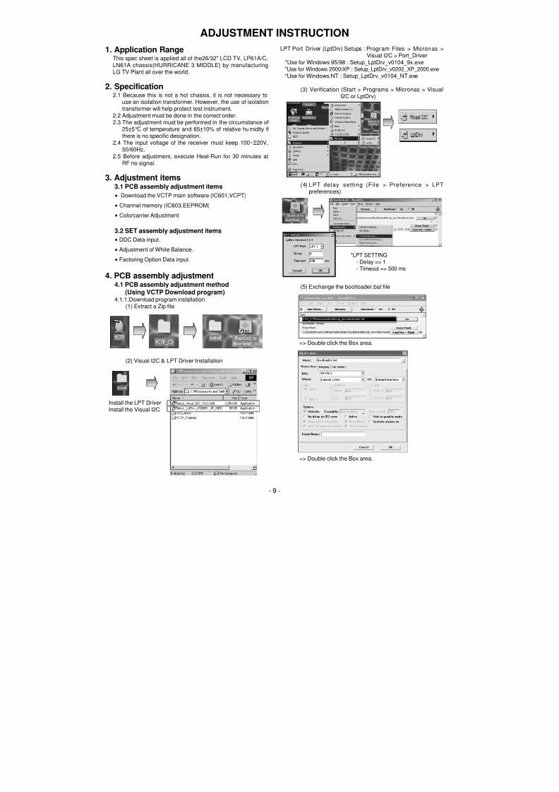
ADJUSTMENT INSTRUCTION
1. Application RangeThis spec sheet is applied all of the26/32" LCD TV, LP61A/C,LN61A chassis(HURRICANE 3 MIDDLE) by manufacturingLG TV Plant all over the world.
2. Specification2.1 Because this is not a hot chassis, it is not necessary to
use an isolation transformer. However, the use of isolationtransformer will help protect test instrument.
2.2 Adjustment must be done in the correct order.2.3 The adjustment must be performed in the circumstance of
25±5°C of temperature and 65±10% of relative humidity ifthere is no specific designation.
2.4 The input voltage of the receiver must keep 100~220V,50/60Hz.
2.5 Before adjustment, execute Heat-Run for 30 minutes atRF no signal.
3. Adjustment items3.1 PCB assembly adjustment items
• Download the VCTP main software (IC601,VCPT)
• Channel memory (IC603,EEPROM)
• Colorcarrier Adjustment
3.2 SET assembly adjustment items
• DDC Data input.
• Adjustment of White Balance.
• Factoring Option Data input.
4. PCB assembly adjustment4.1 PCB assembly adjustment method
(Using VCTP Download program)4.1.1.Download program installation
(1) Extract a Zip file
(2) Visual I2C & LPT Driver Installation
LPT Port Driver (LptDrv) Setups : Program Files > Micronas >Visual I2C > Port_Driver
*Use for Windows 95/98 : Setup_LptDrv_v0104_9x.exe*Use for Windows 2000/XP : Setup_LptDrv_v0202_XP_2000.exe
*Use for Windows NT : Setup_LptDrv_v0104_NT.exe
(3) Verification (Start > Programs > Micronas > VisualI2C or LptDrv)
(4) LPT delay sett ing (File > Preference > LPTpreferences)
(5) Exchange the bootloader.bat file
Install the LPT Driver
Install the Visual I2C
*LPT SETTING
- Delay => 1
- Timeout => 500 ms
=> Double click the Box area.
=> Double click the Box area.

7/22/2019 lg 32LC2R
http://slidepdf.com/reader/full/lg-32lc2r 10/40
- 10 -
4.1.2. S/W program download
• Preliminary steps
4.1.2.1 Download method 1 (PCB Ass’y)
(1) Connect the download jig to D-sub jack
(2) Execute ‘Download.vi2c’ program in PC, then a mainwindow will be opened
(3) Double click the blue box and confirm "BootloaderVersion" as 40.
(4) Click the "Erase Flash" button
(5) Double click the download file low, then "edit"window will be opened
(6) Click the choice button in the "edit window", then"file choice window" will be opened
(7)Choose the Hex f i le in folder and execute
downloading with click " open" button.
=> Select the "Bootloader.bat" f i le(install >VCTP_download > Bootloader)
=> Push "OK"
=> Finish the program, after saving the f i le"download_cs.vi2c"
(if you click , the massage appears automatically)x

7/22/2019 lg 32LC2R
http://slidepdf.com/reader/full/lg-32lc2r 11/40
- 11 -
(8) Click OK button at the "edit window"
(9) Under Downloading process
(10) If download is failed, for example "No acknowledgefrom slave". Execute download again from(1)
4.1.2.2 Download method 2 (AV Plate Ass’y)
(1) Push S/W ‘ON" (connect SCL to GND using switchat Jig ) and connect the download jig to D-sub jack
(2) Supply the power (Stand-by 5V) and wait for 3seconds.
(3) Push the S/W off (Disconnect SCL to GND usingswitch at jig)
(4) Execute ‘Download.vi2c’ program in PC, then a mainwidow will be opened.
(5) Double click the blue box and confirm "BootloaderVersion" as 40.
Push S/W
Double click
Push S/W

7/22/2019 lg 32LC2R
http://slidepdf.com/reader/full/lg-32lc2r 12/40
- 12 -
(6)Click the "Erase Flash" button
(7) Double click the download file low then, "edit"window will be opened
(8) Chick the choice button I n the "edit window", then"file choice window’ will be opened
(9) Choose t he Hex f ile in folder and exe cutedownloading with click "open button"
(10) Click OK button at the "edit window"
(11) Under Downloading progress
(12) If download is failed, for example "No acknowledgefrom slave", execute download again from (1)
4.1.2.2 Download method 3 (SET)(1) Push the "Tilt" button in an Adjust Remocon Then
the LCD TV will change a "slave mode"
(2) Connect Zig to TV using a D-sub cable

7/22/2019 lg 32LC2R
http://slidepdf.com/reader/full/lg-32lc2r 13/40
- 13 -
(3) Execute ‘Download_CS.vi2c’ program in PC, then amain widow will be opened.
(4) Click "GO" button
(5) Double click the blue box and confirm "BootloaderVersion" as 40.
(6)Click the "Erase Flash" button
(7) Double click the download file low then, "edit"window will be opened
(8) Chick the choice button I n the "edit window", then"file choice window’ will be opened
(9) Choose the Hex f ile in folder and exe cutedownloading with click "open button"
(10) Click OK button at the "edit window"
(11) Under Downloading progress
(12) If download is failed, for example "No acknowledgefrom slave", execute download again from (1)
Double click
If you don’t push the "go",
the Hex file would not be
downloaded although the
download proceeds normally
at first glance

7/22/2019 lg 32LC2R
http://slidepdf.com/reader/full/lg-32lc2r 14/40
- 14 -
4.1.2. Channel memory download(1) Connect the download jig to D-sub jack(2) Execute ‘Channal.vi2c’ program in PC, then a main
window will be opened.
(3) Push the button change and select the Channel memorydata
(4) Check the communication is OK or not.=> Push the Read area (Ackn. Check) and check Cyan
area is OK message.
(5) Push the Update NVM from File
4.1.3. Tool Option Area Option ChangeBefore PCBA check, have to change the Tool option andArea optionOption values are below(If on changed the option, the input menu can differ themodel spec.)
The input methods are same as other chassises(Use adj Keyon the Adjust Remocon)
4.1.4. Colorcarrier Adjustment(Inspection process)a. Tuning the RF signalZJ, TJ, CJ : PAL Philips Pattern(with color Bar)MJ : NTSC Digital Pattern(with color Bar)
b. push the "adj" key in the adjustment remocon.
4.2 SET assembly adjustment method*Caution : Each PCB assembly must be checked by check
JIG set.(Because power PCB Assembly damagesto LCD Module, especially be careful)
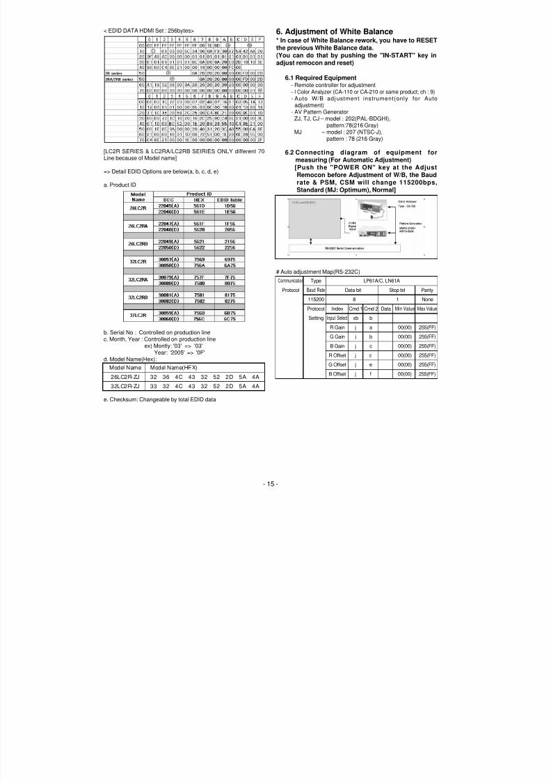
4.2.1 EDID(The Extended Display Identification Data ) / DDC(Display Data Channel) download
* Caution- Use the proper signal cable for EDID Download
* Caution: - Never connect HDMI & D-SUB Cable at thesame time.
- Use the proper cables below for EDID Writing
<EDID DATA Analog Set : 128bytes>
[LC2R SERIES & LC2RA/LC2RB SEIRIES ONLY different 70Line because of Model name]
Tool Option
Inch ZJ TJ CJ
26 30228 25620 25620
32 30229 25621 25621
37 - - 25622
Area Option 17 20 23
7/22/2019 lg 32LC2R
http://slidepdf.com/reader/full/lg-32lc2r 15/40
< EDID DATA HDMI Set : 256bytes>
[LC2R SERIES & LC2RA/LC2RB SEIRIES ONLY different 70Line because of Model name]
=> Detail EDID Options are below(a, b, c, d, e)
a. Product ID
b. Serial No : Controlled on production linec. Month, Year : Controlled on production line
ex) Montly: '03' => '03'Year: '2005' => '0F'
d. Model Name(Hex):
e. Checksum: Changeable by total EDID data
6. Adjustment of White Balance* In case of White Balance rework, you have to RESETthe previous White Balance data.(You can do that by pushing the "IN-START" key inadjust remocon and reset)
6.1 Required Equipment- Remote controller for adjustment- l Color Analyzer (CA-110 or CA-210 or same product; ch : 9)
- Auto W/B adj ustment instrument(only for Autoadjustment)- AV Pattern GeneratorZJ, TJ, CJ – model : 202(PAL-BDGHI),
pattern:78(216 Gray)MJ – model : 207 (NTSC-J),
pattern : 78 (216 Gray)
6.2 Connecting diagram of equipment formeasuring (For Automatic Adjustment)[Push the "POWER ON" key at the AdjustRemocon before Adjustment of W/B, the Baudrate & PSM, CSM will change 115200bps,Standard (MJ: Optimum), Normal]
# Auto adjustment Map(RS-232C)
- 15 -
Model Name Model Name(HEX)
26LC2R-ZJ 32 36 4C 43 32 52 2D 5A 4A
32LC2R-ZJ 33 32 4C 43 32 52 2D 5A 4A
Communication Type LP61A/C, LN61A
Protocol Baud Rate Data bit Stop bit Parity
115200 8 1 NoneProtocol Index Cmd 1 Cmd 2 Data Min Value Max Value
Setting Input Select xb b
R Gain j a 00(00) 255(FF)
G Gain j b 00(00) 255(FF)
B Gain j c 00(00) 255(FF)
R Offset j d 00(00) 255(FF)
G Offset j e 00(00) 255(FF)
B Offset j f 00(00) 255(FF)

7/22/2019 lg 32LC2R
http://slidepdf.com/reader/full/lg-32lc2r 16/40
- 16 -
6.3 Adjustment of White Balance (For Manualadjustment)
- Operate the zero-calibration of the CA-110, then sticksensor to LCD module when you adjust.
- For manual adjustment, it is also possible by the followingsequence
1) Select RF no signal by pressing POWER ON key onremote control for adjustment then operate heat runmore than 15 minutes.(If not executed this step, the condition for W/B will be
differ. The W/B condition is PSM : Standard (MJ :Optimum), CSM : Normal. )
2) As below Fig. 7, Supply 216Level (85 IRE) full screenpattern to Video input.26/32LC2R/2RA/2RB-ZJ : AV3 or AV4(Input 50Hz)26/32LC2R-TJ : AV1or AV2(Input 50Hz),26/32/37LC2R-CJ : AV1 or AV2 (Input 50Hz)26,32LC2R-MJ : VIDEO1 or VIDEO2 (Input 60Hz)
3) Press the POWER ON KEY on R/C for converting inputmode.
4) Enter the White Balance adjustment mode by pressingthe IN-START key (White Balance) on R/C.
5) 5) Stick sensor to center of the screen and select each
items (Red/Green/Blue Gain and Offset) using /
(CH +/-) key on R/C..
6) Adjust Only High Light with R Gain / B Gain using /
(VOL +/-) key on R/C.7) Adjust it until color coordination becomes as below.
(Initially, R/G/B gain and R/G/B offset values are fixed asbelow)
Red Gain : 80 , Green Gain : 80 , Blue Gain : 80Red Offset : 80, Green Offset : 80 , Blue Offset : 80
# Target Value [PSM: Standard(ZJ, TJ, CJ), Optimum(MJ),CSM: Normal]
-Normal (9300K) x ; 0.283±0.003 y ; 0.298±0.003
=> Reference Value(Automatically fixed)- Cool(11000K): x:0.274±0.003, y: 0.286±0.003- Warm(7200K) : x:0.303±0.003, y: 0.319±0.003
Pattern for Adjustment of White Balance
8) When adjustment is completed, Exit adjustment modeusing EXIT key on R/C
6.4 Input the Shipping Option Data1) Push the ADJ key in a Adjust Remocon.2) Input the Option Number that was specified in the BOM,
into the Shipping area.
3) The work is finished, Push Key
216 Level(85 IRE)

7/22/2019 lg 32LC2R
http://slidepdf.com/reader/full/lg-32lc2r 17/40
- 17 -
7. Shipping Conditions
No Item Setting Remarks
1. Station Auto Programme System BG
Storage from 1
Search To start
Manual Programme Storage 1
System BG
Band V/UHF
Channel 69
Fine /
Search /
Name _ _ _ _ _
Programme Edit To set
Favorite programme -- -----
Ch memory TBD TBD
2. Picture PSM Dynamic
CSM Normal For ZJ
Cool For TJ, CJ
For MJ
XD Auto
Advanced Cinema : Off
Black Level : Low Available For HDMI
Reset To Set
3. Sound SSM Flat
AVL Off
TV Speaker On
4. Time Clock --: --
Off Time --: --
Off
On Time --: --
PR 1
Vol. 30
Off
Auto Sleep Off
5. Special Language English Following Buyer's demand, PR
Child Lock Off
Set ID 1
XD Demo To Start
6. Screen Auto Config. To Set Available For RGB-PC mode
Manual Config. Phase 0 Available For RGB-PC modeClock 0
H-Position 0 Available For RGB mode
V-Position 0
XGA Mode 1024x768 Available for RGB-PC XGA 60Hz
ARC 16:9
Reset To set
7/22/2019 lg 32LC2R
http://slidepdf.com/reader/full/lg-32lc2r 18/40
- 18 -
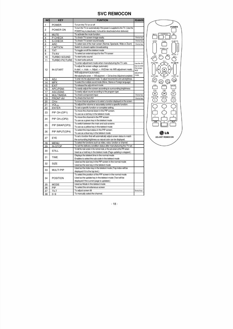
SVC REMOCON
NO KEY FUNTION REAMARK
1 POWER
2 POWER ON
3 MUTE
4 P-CHECK
5 S-CHECK6 ARC
7 CAPTION
8 TXT
9 TV/AV
10 TURBO SOUND
11 TURBO PICTURE
12 IN-START
13 ADJ
14 MPX
15 EXIT
16 APC(PSM)
17 ASC(SSM)
18 MULTIMIDIA
19 FRONT-AV
20 CH
21 VOL
22 ENTER
23 PIP CH-(OP1)
24 PIP CH+(OP2)
25 PIP SWAP(OP3)
26 PIP INPUT(OP4)
27 EYE
28 MENU
29 IN-STOP
30 STILL
31 TIME
32 SIZE
33 MULTI PIP
34 POSITION
35 MODE
36 PIP
37 TILT
38 0~9
To turn the TV on or off
To turn the TV on automatically if the power is supplied to the TV. (Use the
POWER key to deactivate): It should be deactivated when delivered.
To activate the mute function.
To check TV screen image easily.
To check TV screen sound easily
To select size of the main screen (Normal, Spectacle, Wide or Zoom)
Switch to closed caption broadcasting
To toggle on/off the teletext mode
To select an external input for the TV screen
To start turbo sound
To start turbo picture
To enter adjustment mode when manufacturing the TV sets.
To adjust the screen voltage (automatic):
In-start mute Adjust AV(Enter into W/B adjustment mode)
W/B adjustment (automatic):
After adjusting the screen W/B adjustment Exit two times (Adjustment completed)
To enter into the adjustment mode. To adjust horizontal line and sub-brightness.
To select the multiple sound mode (Mono, Stereo or Foreign language)
To release the adjustment mode
To easily adjust the screen according to surrounding brightness
To easily adjust sound according to the program type
To check component input
To check the front AV
To move channel up/down or to select a function displayed on the screen.
To adjust the volume or accurately control a specific function.
To set a specific function or complete setting.
To move the channel down in the PIP screen.
To use as a red key in the teletext mode
To move the channel in the PIP screen
To use as a green key in the teletext mode
To switch between the main and sub screens
To use as a yellow key in the teletext modeTo select the input status in the PIP screen
To use as a blue key in the teletext mode
To set a function that will automatically adjust screen status to match
the surrounding brightness so natural color can be displayed.
To select the functions such as video, voice, function or channel.
To set the delivery condition status after manufacturing the TV set.
To halt the main screen in the normal mode, or the sub screen at the PIP screen.
Used as a hold key in the teletext mode (Page updating is stopped.)
Displays the teletext time in the normal mode
Enables to select the sub code in the teletext mode
Used as the size key in the PIP screen in the normal mode
Used as the size key in the teletext mode
Used as the index key in the teletext mode (Top index will bedisplayed if it is the top text.)
To select the position of the PIP screen in the normal mode
Used as the update key in the teletext mode (Text will be
displayed if the current page is updated.)
Used as Mode in the teletext mode
To select the simultaneous screen
To adjust screen tilt
To manually select the channel.
Shortcut keys
Shortcut keys
Shortcut keys
Use the AVkey to enterthe screenW/Badjustmentmode.
Shortcut keys
Shortcut keys
Shortcut keys
7/22/2019 lg 32LC2R
http://slidepdf.com/reader/full/lg-32lc2r 19/40
- 19 -
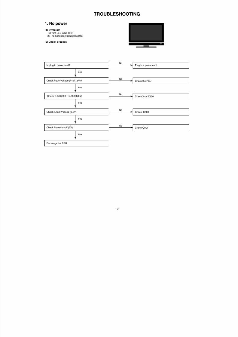
TROUBLESHOOTING
1. No power
(1) Symptom1) Front LED is No light
2) The Set doesnt discharge little
(2) Check process
Is plug in power cord? Plug in a power cordNo
Check the PSUNo
Check X-tal X600No
Check IC600No
Check Q901No
Yes
Check P200 Voltage (P-ST_5V)?
Yes
Check X-tal X600 (19.6608MHz)
Yes
Check IC600 Voltage (3.3V)
Yes
Check Power on/off (5V)
Yes
Exchange the PSU

7/22/2019 lg 32LC2R
http://slidepdf.com/reader/full/lg-32lc2r 20/40
- 20 -
2. No picture
(1) Symptom1) Some mode doesnt display.2) Front LED is green
3) The set still discharge a little
(2) Check follow1) RF-mode doesnt display
Is the LVDS cable
connected?
No
Yes Is the Tuner cable
connected?
No
Yes Are good someelements(C, R, L, orDiode) at path?
No
Yes Are input voltage, I2C,
and CVBS output
good in Tuner?
No
Is VCT-P IC good?
Insert the LVDS
cable exactly
Insert the Tuner
cable exactly
If it dead or short,exchange thiselements
Is the LVDS cableconnected?
No
Yes Are good someelements(C, R, L, orDiode) at path?
No
Yes Is VCT-P IC good?
No
Insert the LVDS
cable exactly
If it dead or short,exchange thiselements
Exchange the VCT-
P IC
Exchange the TunerExchange the VCT-
P IC
No
Yes
Is the LVDS cable
connected?
No
Yes Are good some
elements(C, R, L, orDiode) at path?
No
Yes Check the EDID
data
No
Yes Is AD9381 good?
(only _ HDMI)
No
Is VCT-P IC good?
Insert the LVDS
cable exactly
If it dead or short,
exchange this
elements
Download the EDID
data
Exchange AD9381
IC
Exchange the VCT-
P IC
No
Yes
2) AV/Component-mode doesnt display
3) RGB/HDMI-mode doesnt display

7/22/2019 lg 32LC2R
http://slidepdf.com/reader/full/lg-32lc2r 21/40
- 21 -
3. No Sound
(1) Symptom1) Front LED is Green2) The Set display a screen, but a sound doesnt output
(2) Check follow1) Speaker part
Are Speaker CablesGood?
Are Speaker Cablesconnect normally?
No
Yes
No
Yes Are Speaker unitsgood?
No
Exchange the cableInsert the cableexactly
Exchange the
Speaker unit
Is sound at HDMI
Good?
Is EDID download
good?
No Yes Is IC401 good?
(AD9381)
NoNo
Download EDIDdata once more.
Exchange IC401
Is sound at
Scart1/2 (or
Component2)RGB,
or Side AV Good?
Are good some
elements (C, R, L,
or Diode) at Sound
path?
No
No
Yes YesIs IC800 good?
(Switching IC)
No
If it dead or short,exchange thiselements
Is sound at RF, AV,
or Component1
Good?
Are good some
elements (C, R, L,
or Diode) at Sound
path?
No Yes
No
If it dead or short,exchange thiselements
Exchange IC800
Is IC601 good?
(VCT-P)
No
Exchange IC601
Yes Is IC801 good?
(Amplifier)
No
Exchange IC801
2) Main board part

7/22/2019 lg 32LC2R
http://slidepdf.com/reader/full/lg-32lc2r 22/40
BLOCK DIAGRAM
- 22 -

7/22/2019 lg 32LC2R
http://slidepdf.com/reader/full/lg-32lc2r 23/40
BLOCK DIAGRAM DESCRIPTION
- 23 -
1. Video control and display dataVideo signal is received from TUNER, AV port(AV1,AV2,S-Video) and goes to the one-chip video decoder
(VCTI) which separate the R,G,B signal and passes on the signal to AD converter(AD9883) through the videoswitch(SM5301). Component signal(YPbPr) from side-jack is also passed to video switch(SM5301) and Micom
will select the desired signal(RGB from VCTi or Component from side jack).The AD9883 converts 4:4:4 video format into digital and gives output to the Picture Enhancer (FLI2300).This
picture enhancer improves the quality of the picture by changing the level of RGB/YPbPr signals.The output ofthis enhancer chip is fed to the deinterlacer ,which in turn goes to the Scalar (GM5221).The scalar gives theoutput on the LVDS cable which is connected to LCD module.
VCTi acts a micom and is responsible for video processing and audio signal processing.It accepts the RFprecessed signal(IF signal) from tuner/SAW-Filter and separates sound and picture from it.
Scaler is reponsible for regulating the timing of signal to LCD panel and size and location of the signal. Graphiccontrol accepts the PC(Analog RGB) and DVI-D (Digital) signal. The signal of PC input is connected to analog
port in Scaler and the signal of DVI-D input is connected to digital port. Thus it receives two input and switchbetween them to give output at the LVDS which in turn gives output at the LCD module.
2. PowerThe power board supplies a DC voltage of 33V(main power), 24V(Stand_by power), 12V(Stand_by power) to
the main board. Main power is only available after power-on and Stand_by is always available. 33V is used bythe tuner and 24V is used directly by the inverter and the sound amplifier IC. 24V also is converted into 5V-Main
Power and 5V-Stand_by by a DC/DC Converter(MP1593). The 5V is changed into 3.3V and 1.8V by a regulator.Both voltages(3.3V, 1.8V ) is used by VCTI, Scaler, FLI2300 and AD9883. The voltage of LCD Panel is 12V

7/22/2019 lg 32LC2R
http://slidepdf.com/reader/full/lg-32lc2r 24/40
7/22/2019 lg 32LC2R
http://slidepdf.com/reader/full/lg-32lc2r 25/40
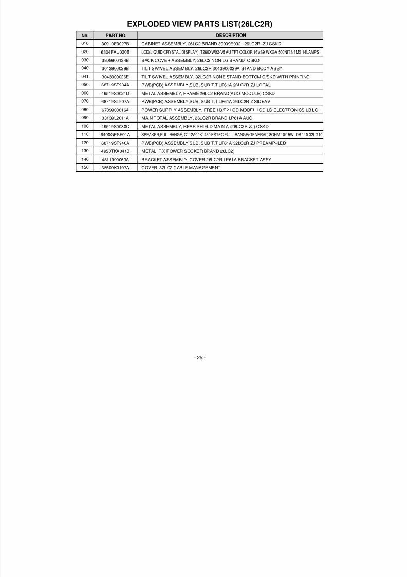
- 25 -
EXPLODED VIEW PARTS LIST(26LC2R)
No. PART NO. DESCRIPTION
30919E0027B CABINET ASSEMBLY, 26LC2 BRAND 30909E0021 26LC2R -ZJ CSKD
6304FAU020B LCD(LIQUID CRYSTAL DISPLAY), T260XW02-V5 AU TFT COLOR 16VS9 WXGA 500NITS 8MS 14LAMPS
3809900134B BACK COVER ASSEMBLY, 26LC2 NON LG BRAND CSKD
3043900029B TILT SWIVEL ASSEMBLY, 26LC2R 3043900029A STAND BODY ASSY
3043900026E TILT SWIVEL ASSEMBLY, 32LC2R NONE STAND BOTTOM C/SKD WITH PRINTING
68719ST934A PWB(PCB) ASSEMBLY,SUB, SUB T.T LP61A 26LC2R ZJ LOCAL
49519S0021D METAL ASSEMBLY, FRAME 26LC2 BRAND(AUO MODULE) CSKD
68719ST907A PWB(PCB) ASSEMBLY,SUB, SUB T.T LP61A 26LC2R Z SIDEAV
6709900016A POWER SUPPLY ASSEMBLY, FREE H3/E2 LCD MODEL LCD LG ELECTRONICS LB LC
33139L2011A MAIN TOTAL ASSEMBLY, 26LC2R BRAND LP61A AUO
49519S0030C METAL ASSEMBLY, REAR SHIELD MAIN A (26LC2R-ZJ) CSKD
6400GESF01A SPEAKER,FULLRANGE, C112A02K1450 ESTEC FULL-RANGE(GENERAL) 8OHM 10/15W .DB 110 32LG10
68719ST940A PWB(PCB) ASSEMBLY,SUB, SUB T.T LP61A 32LC2R ZJ PREAMP+LED
4950TKA041B METAL, FIX POWER SOCKET(BRAND 26LC2)
4811900063A BRACKET ASSEMBLY, COVER 26LC2R LP61A BRACKET ASSY
35509K0197A COVER, 32LC2 CABLE MANAGEMENT
010
020
030
040
041
050
060
070
080
090
100
110
120
130
140
150

7/22/2019 lg 32LC2R
http://slidepdf.com/reader/full/lg-32lc2r 26/40
- 26 -
E X P
L O D E D V I E W ( 3 2 L C 2
R )
0 1 0
0 2 0
0 5 0
0 7 0
0 8 0
0 9 0
1 0 0
0 3 0
1 5 0
0 4 0
0 4 1
1 4 0
1 2 0
1 3 0
0 6 0
0 6 0
1 1 0
7/22/2019 lg 32LC2R
http://slidepdf.com/reader/full/lg-32lc2r 27/40
- 27 -
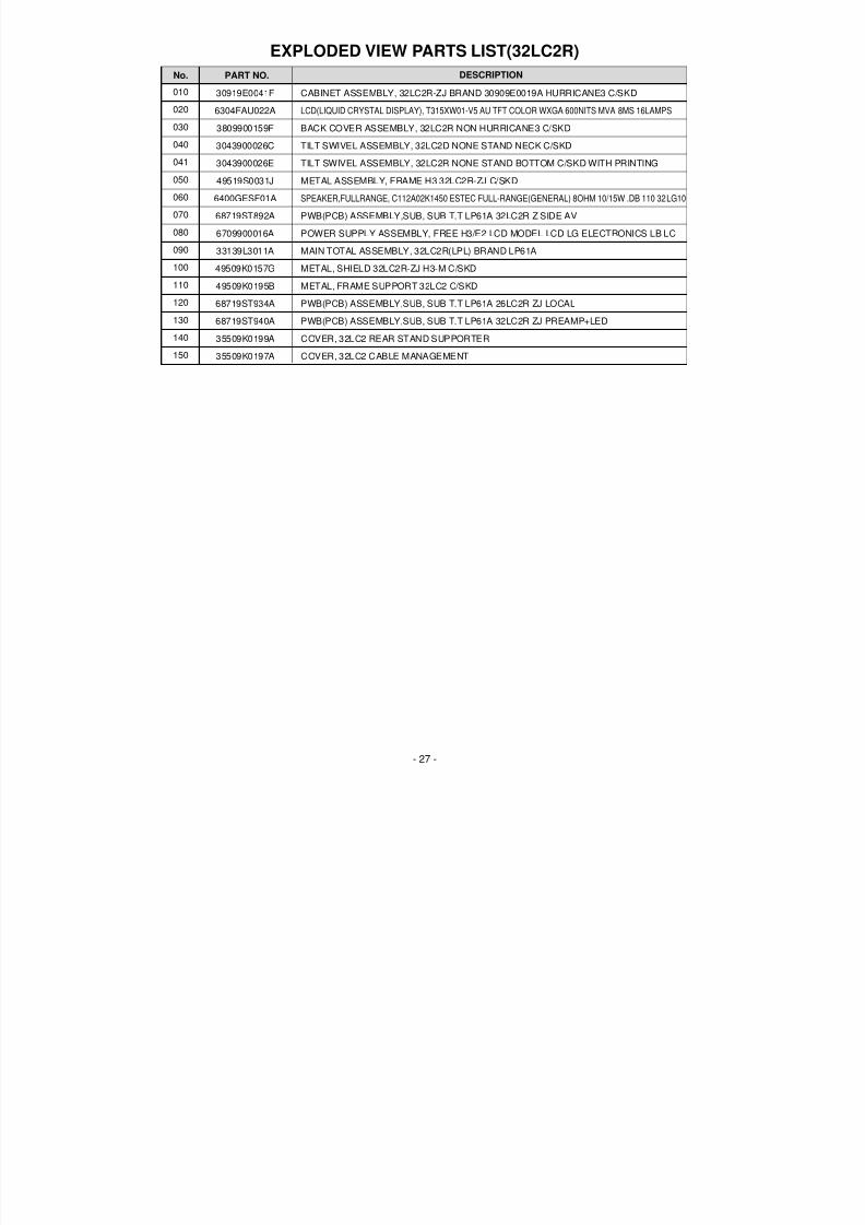
EXPLODED VIEW PARTS LIST(32LC2R)
No. PART NO. DESCRIPTION
30919E0041F CABINET ASSEMBLY, 32LC2R-ZJ BRAND 30909E0019A HURRICANE3 C/SKD
6304FAU022A LCD(LIQUID CRYSTAL DISPLAY), T315XW01-V5 AU TFT COLOR WXGA 600NITS MVA 8MS 16LAMPS
3809900159F BACK COVER ASSEMBLY, 32LC2R NON HURRICANE3 C/SKD
3043900026C TILT SWIVEL ASSEMBLY, 32LC2D NONE STAND NECK C/SKD
3043900026E TILT SWIVEL ASSEMBLY, 32LC2R NONE STAND BOTTOM C/SKD WITH PRINTING
49519S0031J METAL ASSEMBLY, FRAME H3 32LC2R-ZJ C/SKD
6400GESF01A SPEAKER,FULLRANGE, C112A02K1450 ESTEC FULL-RANGE(GENERAL) 8OHM 10/15W .DB 110 32LG10
68719ST892A PWB(PCB) ASSEMBLY,SUB, SUB T.T LP61A 32LC2R Z SIDE AV
6709900016A POWER SUPPLY ASSEMBLY, FREE H3/E2 LCD MODEL LCD LG ELECTRONICS LB LC
33139L3011A MAIN TOTAL ASSEMBLY, 32LC2R(LPL) BRAND LP61A
49509K0157G METAL, SHIELD 32LC2R-ZJ H3-M C/SKD
49509K0195B METAL, FRAME SUPPORT 32LC2 C/SKD
68719ST934A PWB(PCB) ASSEMBLY,SUB, SUB T.T LP61A 26LC2R ZJ LOCAL
68719ST940A PWB(PCB) ASSEMBLY,SUB, SUB T.T LP61A 32LC2R ZJ PREAMP+LED
35509K0199A COVER, 32LC2 REAR STAND SUPPORTER
35509K0197A COVER, 32LC2 CABLE MANAGEMENT
010
020
030
040
041
050
060
070
080
090
100
110
120
130
140
150

7/22/2019 lg 32LC2R
http://slidepdf.com/reader/full/lg-32lc2r 28/40
- 28 -
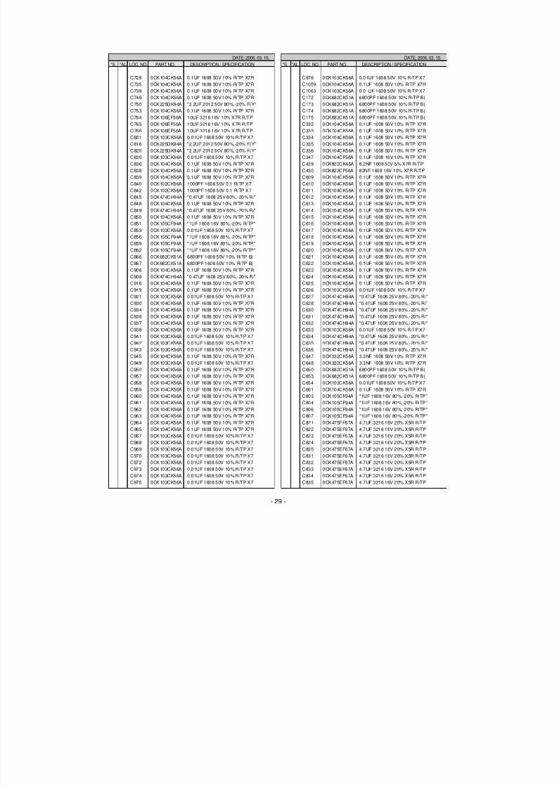
DATE: 2006. 03. 15.
*S *AL LOC. NO. PART NO. DESCRIPTION / SPECIFICATION
C1000 0CK104CK56A 0.1UF 1608 50V 10% R/TP X7R
C1002 0CK104CK56A 0.1UF 1608 50V 10% R/TP X7R
C1004 0CK104CK56A 0.1UF 1608 50V 10% R/TP X7R
C1005 0CK104CK56A 0.1UF 1608 50V 10% R/TP X7R
C1006 0CK103CK56A 0.01UF 1608 50V 10% R/TP X7
C1008 0CK103CK56A 0.01UF 1608 50V 10% R/TP X7
C1011 0CK103CK56A 0.01UF 1608 50V 10% R/TP X7
C1012 0CK104CK56A 0.1UF 1608 50V 10% R/TP X7R
C1013 0CK104CK56A 0.1UF 1608 50V 10% R/TP X7R
C1014 0CK104CK56A 0.1UF 1608 50V 10% R/TP X7RC1015 0CK104CK56A 0.1UF 1608 50V 10% R/TP X7R
C1022 0CK104CK56A 0.1UF 1608 50V 10% R/TP X7R
C1023 0CK104CK56A 0.1UF 1608 50V 10% R/TP X7R
C1024 0CK104CK56A 0.1UF 1608 50V 10% R/TP X7R
C1025 0CK104CK56A 0.1UF 1608 50V 10% R/TP X7R
C1026 0CK103CK56A 0.01UF 1608 50V 10% R/TP X7
C1027 0CK104CK56A 0.1UF 1608 50V 10% R/TP X7R
C1029 0CK103CK56A 0.01UF 1608 50V 10% R/TP X7
C1036 0CK104CK56A 0.1UF 1608 50V 10% R/TP X7R
C1037 0CK104CK56A 0.1UF 1608 50V 10% R/TP X7R
C1039 0CK103CK56A 0.01UF 1608 50V 10% R/TP X7
C1043 0CK104CK56A 0.1UF 1608 50V 10% R/TP X7R
C1045 0CK104CK56A 0.1UF 1608 50V 10% R/TP X7R
C1050 0CK104CK56A 0.1UF 1608 50V 10% R/TP X7R
C1051 0CK104CK56A 0.1UF 1608 50V 10% R/TP X7RC1052 0CK104CK56A 0.1UF 1608 50V 10% R/TP X7R
C1054 0CK104CK56A 0.1UF 1608 50V 10% R/TP X7R
C1056 0CK103CK56A 0.01UF 1608 50V 10% R/TP X7
C1057 0CK103CK56A 0.01UF 1608 50V 10% R/TP X7
C1058 0CK103CK56A 0.01UF 1608 50V 10% R/TP X7
C1061 0CK103CK56A 0.01UF 1608 50V 10% R/TP X7
C1069 0CK104CK56A 0.1UF 1608 50V 10% R/TP X7R
C1072 0CK104CK56A 0.1UF 1608 50V 10% R/TP X7R
C1073 0CK103CK56A 0.01UF 1608 50V 10% R/TP X7
C111 0CK103CK56A 0.01UF 1608 50V 10% R/TP X7
C113 0CK103CK56A 0.01UF 1608 50V 10% R/TP X7
C115 0CK103CK56A 0.01UF 1608 50V 10% R/TP X7
C117 0CK103CK56A 0.01UF 1608 50V 10% R/TP X7
C137 0CK104CK56A 0.1UF 1608 50V 10% R/TP X7R
C138 0CK104CK56A 0.1UF 1608 50V 10% R/TP X7R
C141 0CK104CK56A 0.1UF 1608 50V 10% R/TP X7R
C163 0CK103CK56A 0.01UF 1608 50V 10% R/TP X7
C164 0CK103CK56A 0.01UF 1608 50V 10% R/TP X7
C309 0CK103CK56A 0.01UF 1608 50V 10% R/TP X7
C310 0CK103CK56A 0.01UF 1608 50V 10% R/TP X7
C312 0CK104CK56A 0.1UF 1608 50V 10% R/TP X7R
C337 0CK104CK56A 0.1UF 1608 50V 10% R/TP X7R
C338 0CK104CK56A 0.1UF 1608 50V 10% R/TP X7R
C339 0CK104CK56A 0.1UF 1608 50V 10% R/TP X7R
C350 0CK103CK56A 0.01UF 1608 50V 10% R/TP X7
C351 0CK104CK56A 0.1UF 1608 50V 10% R/TP X7R
C352 0CK104CK56A 0.1UF 1608 50V 10% R/TP X7R
DATE: 2006. 03. 15.
*S *AL LOC. NO. PART NO. DESCRIPTION / SPECIFICATION
C400 0CK104CK56A 0.1UF 1608 50V 10% R/TP X7R
C406 0CK104CK56A 0.1UF 1608 50V 10% R/TP X7R
C407 0CK104CK56A 0.1UF 1608 50V 10% R/TP X7R
C408 0CK104CK56A 0.1UF 1608 50V 10% R/TP X7R
C409 0CK104CK56A 0.1UF 1608 50V 10% R/TP X7R
C410 0CK102CK56A 1000PF 1608 50V 0.1 R/TP X7
C411 0CK102CK56A 1000PF 1608 50V 0.1 R/TP X7
C412 0CK104CK56A 0.1UF 1608 50V 10% R/TP X7R
C413 0CK104CK56A 0.1UF 1608 50V 10% R/TP X7R
C414 0CK104CK56A 0.1UF 1608 50V 10% R/TP X7R
C415 0CK104CK56A 0.1UF 1608 50V 10% R/TP X7R
C416 0CK104CK56A 0.1UF 1608 50V 10% R/TP X7RC417 0CK102CK56A 1000PF 1608 50V 0.1 R/TP X7
C419 0CK104CK56A 0.1UF 1608 50V 10% R/TP X7R
C420 0CK102CK56A 1000PF 1608 50V 0.1 R/TP X7
C421 0CK104CK56A 0.1UF 1608 50V 10% R/TP X7R
C424 0CK104CK56A 0.1UF 1608 50V 10% R/TP X7R
C425 0CK104CK56A 0.1UF 1608 50V 10% R/TP X7R
C426 0CK104CK56A 0.1UF 1608 50V 10% R/TP X7R
C506 0CK103CK56A 0.01UF 1608 50V 10% R/TP X7
C507 0CK103CK56A 0.01UF 1608 50V 10% R/TP X7
C511 0CK103CK56A 0.01UF 1608 50V 10% R/TP X7
C514 0CK273CK56A 27000PF 1608 50V 10% X7R R/
C515 0CK103CK56A 0.01UF 1608 50V 10% R/TP X7
C516 0CK104CK56A 0.1UF 1608 50V 10% R/TP X7R
C517 0CK273CK56A 27000PF 1608 50V 10% X7R R/
C518 0CK104CK56A 0.1UF 1608 50V 10% R/TP X7RC520 0CK104CK56A 0.1UF 1608 50V 10% R/TP X7R
C524 0CK104CK56A 0.1UF 1608 50V 10% R/TP X7R
C605 0CK104CK56A 0.1UF 1608 50V 10% R/TP X7R
C606 0CK104CK56A 0.1UF 1608 50V 10% R/TP X7R
C607 0CK104CK56A 0.1UF 1608 50V 10% R/TP X7R
C608 0CK104CK56A 0.1UF 1608 50V 10% R/TP X7R
C638 0CK104CK56A 0.1UF 1608 50V 10% R/TP X7R
C643 0CK332CK56A 3.3NF 1608 50V 10% R/TP X7R
C645 0CK332CK56A 3.3NF 1608 50V 10% R/TP X7R
C649 0CK104CK56A 0.1UF 1608 50V 10% R/TP X7R
C662 0CK225DK94A "2.2UF 2012 50V 80%,-20% F(Y"
C663 0CK104CK56A 0.1UF 1608 50V 10% R/TP X7R
C664 0CK104CK56A 0.1UF 1608 50V 10% R/TP X7R
C665 0CK225DK94A "2.2UF 2012 50V 80%,-20% F(Y"
C666 0CK225DD66A 2.2UF 2012 10V 20% X7R R/TP
C687 0CK104CK56A 0.1UF 1608 50V 10% R/TP X7R
C688 0CK104CK56A 0.1UF 1608 50V 10% R/TP X7R
C693 0CK104CK56A 0.1UF 1608 50V 10% R/TP X7R
C694 0CK104CK56A 0.1UF 1608 50V 10% R/TP X7R
C695 0CK104CK56A 0.1UF 1608 50V 10% R/TP X7R
C696 0CK104CK56A 0.1UF 1608 50V 10% R/TP X7R
C697 0CK104CK56A 0.1UF 1608 50V 10% R/TP X7R
C704 0CK104CK56A 0.1UF 1608 50V 10% R/TP X7R
C705 0CK104CK56A 0.1UF 1608 50V 10% R/TP X7R
C713 0CK104CK56A 0.1UF 1608 50V 10% R/TP X7R
C721 0CK104CK56A 0.1UF 1608 50V 10% R/TP X7R
C726 0CK104CK56A 0.1UF 1608 50V 10% R/TP X7R
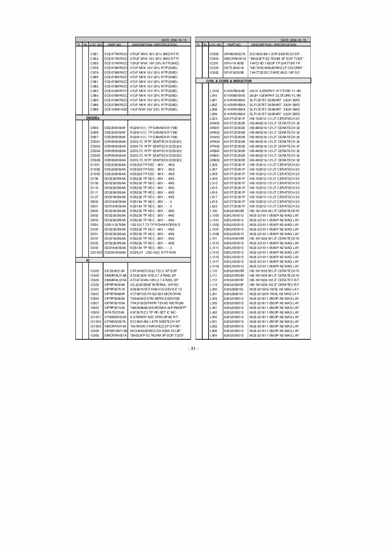
REPLACEMENT PARTS LIST
MAIN BOARD
CAPACITOR
For Capacitor & Resistors, thecharactors at 2nd and 3rd digit in theP/No. means as follows;
CC, CX, CK, CN, CH : CeramicCQ : PolyestorCE : ElectrolyticCF : Fixed Film
RD : Carbon FilmRS : Metal Oxide FilmRN : Metal FilmRH : CHIP, Metal Glazed(Chip)RR : Drawing
7/22/2019 lg 32LC2R
http://slidepdf.com/reader/full/lg-32lc2r 29/40
- 29 -
DATE: 2006. 03. 15.
*S *AL LOC. NO. PART NO. DESCRIPTION / SPECIFICATION
C729 0CK104CK56A 0.1UF 1608 50V 10% R/TP X7R
C735 0CK104CK56A 0.1UF 1608 50V 10% R/TP X7R
C739 0CK104CK56A 0.1UF 1608 50V 10% R/TP X7R
C749 0CK104CK56A 0.1UF 1608 50V 10% R/TP X7R
C750 0CK225DK94A "2.2UF 2012 50V 80%,-20% F(Y"
C753 0CK104CK56A 0.1UF 1608 50V 10% R/TP X7R
C764 0CK106EF56A 10UF 3216 16V 10% X7R R/TP
C765 0CK106EF56A 10UF 3216 16V 10% X7R R/TP
C766 0CK106EF56A 10UF 3216 16V 10% X7R R/TP
C801 0CK103CK56A 0.01UF 1608 50V 10% R/TP X7
C816 0CK225DK94A "2.2UF 2012 50V 80%,-20% F(Y"
C820 0CK225DK94A "2.2UF 2012 50V 80%,-20% F(Y"
C830 0CK103CK56A 0.01UF 1608 50V 10% R/TP X7
C836 0CK104CK56A 0.1UF 1608 50V 10% R/TP X7R
C838 0CK104CK56A 0.1UF 1608 50V 10% R/TP X7R
C839 0CK104CK56A 0.1UF 1608 50V 10% R/TP X7R
C840 0CK102CK56A 1000PF 1608 50V 0.1 R/TP X7
C842 0CK102CK56A 1000PF 1608 50V 0.1 R/TP X7
C845 0CK474CH94A "0.47UF 1608 25V 80%,-20% R/"
C848 0CK104CK56A 0.1UF 1608 50V 10% R/TP X7R
C849 0CK474CH94A "0.47UF 1608 25V 80%,-20% R/"
C850 0CK104CK56A 0.1UF 1608 50V 10% R/TP X7R
C851 0CK105CF94A "1UF 1608 16V 80%,-20% R/TP"
C853 0CK103CK56A 0.01UF 1608 50V 10% R/TP X7
C856 0CK105CF94A "1UF 1608 16V 80%,-20% R/TP"
C859 0CK105CF94A "1UF 1608 16V 80%,-20% R/TP"
C862 0CK105CF94A "1UF 1608 16V 80%,-20% R/TP"
C866 0CK682CK51A 6800PF 1608 50V 10% R/TP B(
C867 0CK682CK51A 6800PF 1608 50V 10% R/TP B(
C906 0CK104CK56A 0.1UF 1608 50V 10% R/TP X7R
C908 0CK474CH94A "0.47UF 1608 25V 80%,-20% R/"
C916 0CK104CK56A 0.1UF 1608 50V 10% R/TP X7R
C919 0CK104CK56A 0.1UF 1608 50V 10% R/TP X7R
C921 0CK103CK56A 0.01UF 1608 50V 10% R/TP X7
C930 0CK104CK56A 0.1UF 1608 50V 10% R/TP X7RC934 0CK104CK56A 0.1UF 1608 50V 10% R/TP X7R
C936 0CK104CK56A 0.1UF 1608 50V 10% R/TP X7R
C937 0CK104CK56A 0.1UF 1608 50V 10% R/TP X7R
C938 0CK104CK56A 0.1UF 1608 50V 10% R/TP X7R
C941 0CK103CK56A 0.01UF 1608 50V 10% R/TP X7
C942 0CK103CK56A 0.01UF 1608 50V 10% R/TP X7
C943 0CK103CK56A 0.01UF 1608 50V 10% R/TP X7
C945 0CK104CK56A 0.1UF 1608 50V 10% R/TP X7R
C949 0CK103CK56A 0.01UF 1608 50V 10% R/TP X7
C950 0CK104CK56A 0.1UF 1608 50V 10% R/TP X7R
C957 0CK104CK56A 0.1UF 1608 50V 10% R/TP X7R
C958 0CK104CK56A 0.1UF 1608 50V 10% R/TP X7R
C959 0CK104CK56A 0.1UF 1608 50V 10% R/TP X7R
C960 0CK104CK56A 0.1UF 1608 50V 10% R/TP X7R
C961 0CK104CK56A 0.1UF 1608 50V 10% R/TP X7RC962 0CK104CK56A 0.1UF 1608 50V 10% R/TP X7R
C963 0CK104CK56A 0.1UF 1608 50V 10% R/TP X7R
C964 0CK104CK56A 0.1UF 1608 50V 10% R/TP X7R
C965 0CK104CK56A 0.1UF 1608 50V 10% R/TP X7R
C967 0CK103CK56A 0.01UF 1608 50V 10% R/TP X7
C968 0CK103CK56A 0.01UF 1608 50V 10% R/TP X7
C969 0CK103CK56A 0.01UF 1608 50V 10% R/TP X7
C970 0CK103CK56A 0.01UF 1608 50V 10% R/TP X7
C972 0CK103CK56A 0.01UF 1608 50V 10% R/TP X7
C973 0CK103CK56A 0.01UF 1608 50V 10% R/TP X7
C974 0CK103CK56A 0.01UF 1608 50V 10% R/TP X7
C975 0CK103CK56A 0.01UF 1608 50V 10% R/TP X7
DATE: 2006. 03. 15.
*S *AL LOC. NO. PART NO. DESCRIPTION / SPECIFICATION
C976 0CK103CK56A 0.01UF 1608 50V 10% R/TP X7
C1059 0CK104CK56A 0.1UF 1608 50V 10% R/TP X7R
C1063 0CK103CK56A 0.01UF 1608 50V 10% R/TP X7
C172 0CK682CK51A 6800PF 1608 50V 10% R/TP B(
C173 0CK682CK51A 6800PF 1608 50V 10% R/TP B(
C174 0CK682CK51A 6800PF 1608 50V 10% R/TP B(
C175 0CK682CK51A 6800PF 1608 50V 10% R/TP B(
C332 0CK104CK56A 0.1UF 1608 50V 10% R/TP X7R
C333 0CK104CK56A 0.1UF 1608 50V 10% R/TP X7R
C334 0CK104CK56A 0.1UF 1608 50V 10% R/TP X7R
C335 0CK104CK56A 0.1UF 1608 50V 10% R/TP X7R
C336 0CK104CK56A 0.1UF 1608 50V 10% R/TP X7R
C347 0CK104CF56A 0.1UF 1608 16V 10% R/TP X7R
C429 0CK822CK46A 8.2NF 1608 50V 5% X7R R/TP
C430 0CK823CF56A 82NF 1608 16V 10% X7R R/TP
C609 0CK104CK56A 0.1UF 1608 50V 10% R/TP X7R
C610 0CK104CK56A 0.1UF 1608 50V 10% R/TP X7R
C611 0CK104CK56A 0.1UF 1608 50V 10% R/TP X7R
C612 0CK104CK56A 0.1UF 1608 50V 10% R/TP X7R
C613 0CK104CK56A 0.1UF 1608 50V 10% R/TP X7R
C614 0CK104CK56A 0.1UF 1608 50V 10% R/TP X7R
C615 0CK104CK56A 0.1UF 1608 50V 10% R/TP X7R
C616 0CK104CK56A 0.1UF 1608 50V 10% R/TP X7R
C617 0CK104CK56A 0.1UF 1608 50V 10% R/TP X7R
C618 0CK104CK56A 0.1UF 1608 50V 10% R/TP X7R
C619 0CK104CK56A 0.1UF 1608 50V 10% R/TP X7R
C620 0CK104CK56A 0.1UF 1608 50V 10% R/TP X7R
C621 0CK104CK56A 0.1UF 1608 50V 10% R/TP X7R
C622 0CK104CK56A 0.1UF 1608 50V 10% R/TP X7R
C623 0CK104CK56A 0.1UF 1608 50V 10% R/TP X7R
C624 0CK104CK56A 0.1UF 1608 50V 10% R/TP X7R
C625 0CK104CK56A 0.1UF 1608 50V 10% R/TP X7R
C626 0CK103CK56A 0.01UF 1608 50V 10% R/TP X7
C627 0CK474CH94A "0.47UF 1608 25V 80%,-20% R/"
C628 0CK474CH94A "0.47UF 1608 25V 80%,-20% R/"C630 0CK474CH94A "0.47UF 1608 25V 80%,-20% R/"
C631 0CK474CH94A "0.47UF 1608 25V 80%,-20% R/"
C632 0CK474CH94A "0.47UF 1608 25V 80%,-20% R/"
C633 0CK103CK56A 0.01UF 1608 50V 10% R/TP X7
C634 0CK474CH94A "0.47UF 1608 25V 80%,-20% R/"
C635 0CK474CH94A "0.47UF 1608 25V 80%,-20% R/"
C636 0CK474CH94A "0.47UF 1608 25V 80%,-20% R/"
C647 0CK332CK56A 3.3NF 1608 50V 10% R/TP X7R
C648 0CK332CK56A 3.3NF 1608 50V 10% R/TP X7R
C650 0CK682CK51A 6800PF 1608 50V 10% R/TP B(
C653 0CK682CK51A 6800PF 1608 50V 10% R/TP B(
C654 0CK103CK56A 0.01UF 1608 50V 10% R/TP X7
C661 0CK104CK56A 0.1UF 1608 50V 10% R/TP X7R
C803 0CK105CF94A "1UF 1608 16V 80%,-20% R/TP"
C804 0CK105CF94A "1UF 1608 16V 80%,-20% R/TP"C806 0CK105CF94A "1UF 1608 16V 80%,-20% R/TP"
C807 0CK105CF94A "1UF 1608 16V 80%,-20% R/TP"
C821 0CK475EF67A 4.7UF 3216 16V 20% X5R R/TP
C822 0CK475EF67A 4.7UF 3216 16V 20% X5R R/TP
C823 0CK475EF67A 4.7UF 3216 16V 20% X5R R/TP
C824 0CK475EF67A 4.7UF 3216 16V 20% X5R R/TP
C825 0CK475EF67A 4.7UF 3216 16V 20% X5R R/TP
C831 0CK475EF67A 4.7UF 3216 16V 20% X5R R/TP
C832 0CK475EF67A 4.7UF 3216 16V 20% X5R R/TP
C833 0CK475EF67A 4.7UF 3216 16V 20% X5R R/TP
C834 0CK475EF67A 4.7UF 3216 16V 20% X5R R/TP
C835 0CK475EF67A 4.7UF 3216 16V 20% X5R R/TP

7/22/2019 lg 32LC2R
http://slidepdf.com/reader/full/lg-32lc2r 30/40
DATE: 2006. 03. 15.
*S *AL LOC. NO. PART NO. DESCRIPTION / SPECIFICATION
C854 0CK224CF56A 0.22UF 1608 16V 10% R/TP X7
C855 0CK224CF56A 0.22UF 1608 16V 10% R/TP X7
C857 0CK105CF94A "1UF 1608 16V 80%,-20% R/TP"
C858 0CK105CF94A "1UF 1608 16V 80%,-20% R/TP"
C864 0CK224CF56A 0.22UF 1608 16V 10% R/TP X7
C865 0CK224CF56A 0.22UF 1608 16V 10% R/TP X7
C915 0CK474CH94A "0.47UF 1608 25V 80%,-20% R/"
C926 0CK104CK56A 0.1UF 1608 50V 10% R/TP X7R
C927 0CK104CK56A 0.1UF 1608 50V 10% R/TP X7R
C928 0CK103CK56A 0.01UF 1608 50V 10% R/TP X7
C929 0CK103CK56A 0.01UF 1608 50V 10% R/TP X7
C989 0CK103CK56A 0.01UF 1608 50V 10% R/TP X7
C112 0CC102CK41A 1000PF 1608 50V 5% R/TP NP0
C114 0CC102CK41A 1000PF 1608 50V 5% R/TP NP0
C116 0CC102CK41A 1000PF 1608 50V 5% R/TP NP0
C120 0CC102CK41A 1000PF 1608 50V 5% R/TP NP0
C311 0CC470CK41A 47PF 1608 50V 5% R/TP NP0
C316 0CC120CK41A 12PF 1608 50V 5% R/TP NP0
C317 0CC120CK41A 12PF 1608 50V 5% R/TP NP0
C508 0CC270CK41A 27PF 1608 50V 5% R/TP NP0
C509 0CC270CK41A 27PF 1608 50V 5% R/TP NP0
C512 0CC101CK41A 100PF 1608 50V 5% R/TP NP0
C521 0CC271CK41A 270PF 1608 50V 5% R/TP NP0
C652 0CC560CK41A 56PF 1608 50V 5% R/TP NP0
C827 0CC471CK41A 470PF 1608 50V 5% R/TP NP0
C829 0CC471CK41A 470PF 1608 50V 5% R/TP NP0
C522 0CC271CK41A 270PF 1608 50V 5% R/TP NP0
C651 0CC560CK41A 56PF 1608 50V 5% R/TP NP0
C655 0CC220CK41A 22PF 1608 50V 5% R/TP NP0
C673 0CC220CK41A 22PF 1608 50V 5% R/TP NP0
C674 0CC220CK41A 22PF 1608 50V 5% R/TP NP0
C1016 0CE477EJ618 470UF KMG 35V 20% FL TP 5
C1020 0CE477EJ618 470UF KMG 35V 20% FL TP 5
C1001 0CE107WF6DC 100UF MVK 16V 20% R/TP(SMD)
C1003 0CE107WF6DC 100UF MVK 16V 20% R/TP(SMD)C1007 0CE107WF6DC 100UF MVK 16V 20% R/TP(SMD)
C1009 0CE107WF6DC 100UF MVK 16V 20% R/TP(SMD)
C1010 0CE107WF6DC 100UF MVK 16V 20% R/TP(SMD)
C1017 0CE477WF6DC 470UF MVK 16V 20% SMD R/TP(
C1018 0CE227WF6DC 220UF MVK 16V 20% R/TP(SMD)
C1019 0CE477WF6DC 470UF MVK 16V 20% SMD R/TP(
C1021 0CE227WF6DC 220UF MVK 16V 20% R/TP(SMD)
C1031 0CE107WF6DC 100UF MVK 16V 20% R/TP(SMD)
C1038 0CE477WF6DC 470UF MVK 16V 20% SMD R/TP(
C1040 0CE476WF6DC 47UF MVK 16V 20% R/TP(SMD)
C1046 0CE477WF6DC 470UF MVK 16V 20% SMD R/TP(
C1047 0CE107WF6DC 100UF MVK 16V 20% R/TP(SMD)
C1048 0CE107WF6DC 100UF MVK 16V 20% R/TP(SMD)
C1064 0CE107WF6DC 100UF MVK 16V 20% R/TP(SMD)
C1065 0CE107WF6DC 100UF MVK 16V 20% R/TP(SMD)C1066 0CE107WF6DC 100UF MVK 16V 20% R/TP(SMD)
C1068 0CE107WF6DC 100UF MVK 16V 20% R/TP(SMD)
C1070 0CE476WF6DC 47UF MVK 16V 20% R/TP(SMD)
C1071 0CE227WF6DC 220UF MVK 16V 20% R/TP(SMD)
C1074 0CE107WF6DC 100UF MVK 16V 20% R/TP(SMD)
C118 0CE227WF6DC 220UF MVK 16V 20% R/TP(SMD)
C119 0CE227WF6DC 220UF MVK 16V 20% R/TP(SMD)
C124 0CE227WF6DC 220UF MVK 16V 20% R/TP(SMD)
C125 0CE227WF6DC 220UF MVK 16V 20% R/TP(SMD)
C126 0CE106WH6DC 10UF MVK 25V 20% R/TP(SMD)
C128 0CE106WH6DC 10UF MVK 25V 20% R/TP(SMD)
C131 0CE476WF6DC 47UF MVK 16V 20% R/TP(SMD)
DATE: 2006. 03. 15.
*S *AL LOC. NO. PART NO. DESCRIPTION / SPECIFICATION
C134 0CE106WH6DC 10UF MVK 25V 20% R/TP(SMD)
C135 0CE106WH6DC 10UF MVK 25V 20% R/TP(SMD)
C142 0CE476WF6DC 47UF MVK 16V 20% R/TP(SMD)
C313 0CE476WF6DC 47UF MVK 16V 20% R/TP(SMD)
C340 0CE107WF6DC 100UF MVK 16V 20% R/TP(SMD)
C343 0CE476WF6DC 47UF MVK 16V 20% R/TP(SMD)
C345 0CE226WF6DC 22UF MVK 16V 20% R/TP(SMD)
C346 0CE476WF6DC 47UF MVK 16V 20% R/TP(SMD)
C401 0CE476WF6DC 47UF MVK 16V 20% R/TP(SMD)
C500 0CE477WF6DC 470UF MVK 16V 20% SMD R/TP(
C502 0CE477WF6DC 470UF MVK 16V 20% SMD R/TP(
C503 0CE475SK6DC 4.7UF MVG 50V 20% SMD R/TP
C513 0CE477WF6DC 470UF MVK 16V 20% SMD R/TP(
C519 0CE107WF6DC 100UF MVK 16V 20% R/TP(SMD)
C523 0CE476WK6DC 47UF MVK 50V 20% R/TP(SMD)
C525 0CE107WF6DC 100UF MVK 16V 20% R/TP(SMD)
C604 0CE227WF6DC 220UF MVK 16V 20% R/TP(SMD)
C629 0CE475WJ6DC 4.7UF MVK 35V 20% R/TP(SMD)
C637 0CE335WK6D8 "3.3UF MVK,RC 50V 20% SMD TA"
C657 0CE226WF6DC 22UF MVK 16V 20% R/TP(SMD)
C658 0CE226WF6DC 22UF MVK 16V 20% R/TP(SMD)
C659 0CE226WF6DC 22UF MVK 16V 20% R/TP(SMD)
C660 0CE226WF6DC 22UF MVK 16V 20% R/TP(SMD)
C676 0CE226WF6DC 22UF MVK 16V 20% R/TP(SMD)
C677 0CE226WF6DC 22UF MVK 16V 20% R/TP(SMD)
C682 0CE226WF6DC 22UF MVK 16V 20% R/TP(SMD)
C683 0CE226WF6DC 22UF MVK 16V 20% R/TP(SMD)
C684 0CE226WF6DC 22UF MVK 16V 20% R/TP(SMD)
C685 0CE226WF6DC 22UF MVK 16V 20% R/TP(SMD)
C686 0CE226WF6DC 22UF MVK 16V 20% R/TP(SMD)
C719 0CE226WF6DC 22UF MVK 16V 20% R/TP(SMD)
C727 0CE226WF6DC 22UF MVK 16V 20% R/TP(SMD)
C733 0CE226WF6DC 22UF MVK 16V 20% R/TP(SMD)
C743 0CE226WF6DC 22UF MVK 16V 20% R/TP(SMD)
C744 0CE226WF6DC 22UF MVK 16V 20% R/TP(SMD)C756 0CE476WF6DC 47UF MVK 16V 20% R/TP(SMD)
C757 0CE106WH6DC 10UF MVK 25V 20% R/TP(SMD)
C758 0CE476WF6DC 47UF MVK 16V 20% R/TP(SMD)
C759 0CE476WF6DC 47UF MVK 16V 20% R/TP(SMD)
C760 0CE476WF6DC 47UF MVK 16V 20% R/TP(SMD)
C761 0CE476WF6DC 47UF MVK 16V 20% R/TP(SMD)
C762 0CE476WF6DC 47UF MVK 16V 20% R/TP(SMD)
C763 0CE476WF6DC 47UF MVK 16V 20% R/TP(SMD)
C800 0CE107WF6DC 100UF MVK 16V 20% R/TP(SMD)
C802 0CE226WF6DC 22UF MVK 16V 20% R/TP(SMD)
C828 0CE107WK6DC 100UF MVK 50V 20% R/TP(SMD)
C860 0CE227WJ6DC 220UF MVK/RC 35V 20% SMD TA
C861 0CE227WJ6DC 220UF MVK/RC 35V 20% SMD TA
C863 0CE106WH6DC 10UF MVK 25V 20% R/TP(SMD)
C868 0CE475WJ6DC 4.7UF MVK 35V 20% R/TP(SMD)C869 0CE475WJ6DC 4.7UF MVK 35V 20% R/TP(SMD)
C912 0CE476WF6DC 47UF MVK 16V 20% R/TP(SMD)
C917 0CE477WF6DC 470UF MVK 16V 20% SMD R/TP(
C922 0CE476WF6DC 47UF MVK 16V 20% R/TP(SMD)
C931 0CE476WF6DC 47UF MVK 16V 20% R/TP(SMD)
C932 0CE476WF6DC 47UF MVK 16V 20% R/TP(SMD)
C933 0CE477WF6DC 470UF MVK 16V 20% SMD R/TP(
C935 0CE477WF6DC 470UF MVK 16V 20% SMD R/TP(
C939 0CE477WF6DC 470UF MVK 16V 20% SMD R/TP(
C946 0CE107WF6DC 100UF MVK 16V 20% R/TP(SMD)
C947 0CE107WF6DC 100UF MVK 16V 20% R/TP(SMD)
C948 0CE107WF6DC 100UF MVK 16V 20% R/TP(SMD)
- 30 -
7/22/2019 lg 32LC2R
http://slidepdf.com/reader/full/lg-32lc2r 31/40
DATE: 2006. 03. 15.
*S *AL LOC. NO. PART NO. DESCRIPTION / SPECIFICATION
C951 0CE477WF6DC 470UF MVK 16V 20% SMD R/TP(
C953 0CE477WF6DC 470UF MVK 16V 20% SMD R/TP(
C955 0CE107WF6DC 100UF MVK 16V 20% R/TP(SMD)
C978 0CE476WF6DC 47UF MVK 16V 20% R/TP(SMD)
C979 0CE476WF6DC 47UF MVK 16V 20% R/TP(SMD)
C980 0CE476WF6DC 47UF MVK 16V 20% R/TP(SMD)
C981 0CE476WF6DC 47UF MVK 16V 20% R/TP(SMD)
C982 0CE476WF6DC 47UF MVK 16V 20% R/TP(SMD)
C983 0CE476WF6DC 47UF MVK 16V 20% R/TP(SMD)
C984 0CE476WF6DC 47UF MVK 16V 20% R/TP(SMD)
C985 0CE476WF6DC 47UF MVK 16V 20% R/TP(SMD)
C986 0CE476WF6DC 47UF MVK 16V 20% R/TP(SMD)
C988 0CE106WH6DC 10UF MVK 25V 20% R/TP(SMD)
D905 0DD200009AF RU2M V(1) TP SANKEN R-TMD
D906 0DD200009AF RU2M V(1) TP SANKEN R-TMD
D907 0DD200009AF RU2M V(1) TP SANKEN R-TMD
ZD301 0DR050008AA SD05.TC R/TP SEMTECH SOD323
ZD303 0DR050008AA SD05.TC R/TP SEMTECH SOD323
ZD304 0DR050008AA SD05.TC R/TP SEMTECH SOD323
ZD305 0DR050008AA SD05.TC R/TP SEMTECH SOD323
ZD308 0DR050008AA SD05.TC R/TP SEMTECH SOD323
D1001 0DS226009AA KDS226 TP KEC - 80V - - 4NS
D1002 0DS226009AA KDS226 TP KEC - 80V - - 4NS
D1003 0DS226009AA KDS226 TP KEC - 80V - - 4NS
D108 0DS226009AA KDS226 TP KEC - 80V - - 4NS
D109 0DS226009AA KDS226 TP KEC - 80V - - 4NS
D110 0DS226009AA KDS226 TP KEC - 80V - - 4NS
D111 0DS226009AA KDS226 TP KEC - 80V - - 4NS
D127 0DS226009AA KDS226 TP KEC - 80V - - 4NS
D800 0DD184009AA KDS184 TP KEC - 85V - - - 3
D801 0DD184009AA KDS184 TP KEC - 85V - - - 3
D900 0DS226009AA KDS226 TP KEC - 80V - - 4NSD902 0DS226009AA KDS226 TP KEC - 80V - - 4NS
D903 0DS226009AA KDS226 TP KEC - 80V - - 4NS
D500 0DS113379BA 1SS133 T-72 TP ROHM KOREA D
D300 0DS226009AA KDS226 TP KEC - 80V - - 4NS
D301 0DS226009AA KDS226 TP KEC - 80V - - 4NS
D302 0DS226009AA KDS226 TP KEC - 80V - - 4NS
D303 0DS226009AA KDS226 TP KEC - 80V - - 4NS
D400 0DD184009AA KDS184 TP KEC - 85V - - - 3
ZD1000 0DZKE00048A KDZ8.2V USC KEC R/TP NON
IC300 0ICS240213A CAT24W(F)C02J-TE13 8P SOP
IC400 0IMMRAL014B AT24C02N-10SI-2.7 ATMEL 8P
IC603 0IMMRAL025A AT24C32AN-10SI-2.7 ATMEL 8PIC302 0IPRP00009A ICL3232CBNZ INTERSIL 16P/SO
IC401 0IPRP00701A AD9381KSTZ ANALOG DEVICE 10
IC601 0IPRP00689A VCT6973G-FA-B2-000 MICRONAS
IC800 0IPRP00665A TEA6420D STM 28PIN SO28 REE
IC801 0IPRP00700A TPA3100D2PHPR TEXAS INSTRUM
IC802 0IPRP00743A "MAD4868A MICRONAS 44P,PMQFP"
IC600 0IFA752700A KA75270Z 3 TP RE-SET IC MC-
IC1001 0IPMGKE030A KIA78R05F KEC 5PIN DPAK R/T
IC1002 0IPMG00027A SC156515M-1.8TR SEMTECH 5P/
IC1003 0IMCRFA010A "KA7809R, FAIRCHILD 2P D-PAK"
IC500 0IPMGON013B MC34063ADR2G ON SEMI SO-8P
IC900 0IMCRRH001A "BA033FP-E2 ROHM 3P-SOP,TO25"
DATE: 2006. 03. 15.
*S *AL LOC. NO. PART NO. DESCRIPTION / SPECIFICATION
IC902 0IPMG00027A SC156515M-1.8TR SEMTECH 5P/
IC903 0IMCRRH001A "BA033FP-E2 ROHM 3P-SOP,TO25"
IC301 0IPH741400E 74HC14D 14SOP TP SHITTER TR
IC303 0ISTL00031A "MC74HC4066ADR2G,LF ON SEMI"
IC602 0IFA742530B 74ACT253SC FAIRCHILD 16P SO
L1004 6140VB0004B 26UH 1UEWPHY 22.5TURN YL-9N
L910 6140VB0004B 26UH 1UEWPHY 22.5TURN YL-9N
L801 6140VR0008A SLF12575T-330M4R7 33UH SMD
L802 6140VR0008A SLF12575T-330M4R7 33UH SMD
L808 6140VR0008A SLF12575T-330M4R7 33UH SMD
L809 6140VR0008A SLF12575T-330M4R7 33UH SMD
L923 6210TCE001P HB-1S2012-121JT CERATECH 20
AR400 6210TCE002B HB-4M3216-121JT CERATECH 32
AR401 6210TCE002B HB-4M3216-121JT CERATECH 32
AR402 6210TCE002B HB-4M3216-121JT CERATECH 32
AR403 6210TCE002B HB-4M3216-121JT CERATECH 32
AR404 6210TCE002B HB-4M3216-121JT CERATECH 32
AR405 6210TCE002B HB-4M3216-121JT CERATECH 32
AR600 6210TCE002B HB-4M3216-121JT CERATECH 32
AR601 6210TCE002B HB-4M3216-121JT CERATECH 32
AR602 6210TCE002B HB-4M3216-121JT CERATECH 32
L306 6210TCE001P HB-1S2012-121JT CERATECH 20
L307 6210TCE001P HB-1S2012-121JT CERATECH 20
L308 6210TCE001P HB-1S2012-121JT CERATECH 20
L309 6210TCE001P HB-1S2012-121JT CERATECH 20
L310 6210TCE001P HB-1S2012-121JT CERATECH 20
L815 6210TCE001P HB-1S2012-121JT CERATECH 20
L816 6210TCE001P HB-1S2012-121JT CERATECH 20
L817 6210TCE001P HB-1S2012-121JT CERATECH 20
L818 6210TCE001P HB-1S2012-121JT CERATECH 20
L922 6210TCE001P HB-1S2012-121JT CERATECH 20
L100 6200J00005R HB-1M1608-501JT CERATECH R/ L1000 6200J000013 MLB-321611-0500P-N2 MAG LAY
L1001 6200J000013 MLB-321611-0500P-N2 MAG LAY
L1002 6200J000013 MLB-321611-0500P-N2 MAG LAY
L1007 6200J000013 MLB-321611-0500P-N2 MAG LAY
L1008 6200J000013 MLB-321611-0500P-N2 MAG LAY
L101 6200J00005R HB-1M1608-501JT CERATECH R/
L1010 6200J000013 MLB-321611-0500P-N2 MAG LAY
L1011 6200J000013 MLB-321611-0500P-N2 MAG LAY
L1012 6200J000013 MLB-321611-0500P-N2 MAG LAY
L1015 6200J000013 MLB-321611-0500P-N2 MAG LAY
L1017 6200J000013 MLB-321611-0500P-N2 MAG LAY
L1018 6200J000013 MLB-321611-0500P-N2 MAG LAY
L110 6200J00005R HB-1M1608-501JT CERATECH R/
L111 6200J00005R HB-1M1608-501JT CERATECH R/
L112 6200J00005F HB-1M1608-102JT CERATEC R/TL113 6200J00005F HB-1M1608-102JT CERATEC R/T
L300 6200JB8010L MLB-201209-1000L-N2 MAG LAY
L301 6200JB8010L MLB-201209-1000L-N2 MAG LAY
L303 6200J000013 MLB-321611-0500P-N2 MAG LAY
L305 6200J000013 MLB-321611-0500P-N2 MAG LAY
L401 6200J000013 MLB-321611-0500P-N2 MAG LAY
L402 6200J000013 MLB-321611-0500P-N2 MAG LAY
L500 6200J000013 MLB-321611-0500P-N2 MAG LAY
L501 6200J000013 MLB-321611-0500P-N2 MAG LAY
L502 6200J000013 MLB-321611-0500P-N2 MAG LAY
L806 6200J000013 MLB-321611-0500P-N2 MAG LAY
L904 6200J000013 MLB-321611-0500P-N2 MAG LAY
- 31 -
DIODEs
IC
COIL & CORE & INDUCTOR
7/22/2019 lg 32LC2R
http://slidepdf.com/reader/full/lg-32lc2r 32/40
DATE: 2006. 03. 15.
*S *AL LOC. NO. PART NO. DESCRIPTION / SPECIFICATION
L913 6200J000013 MLB-321611-0500P-N2 MAG LAY
L914 6200J000013 MLB-321611-0500P-N2 MAG LAY
L915 6200J000013 MLB-321611-0500P-N2 MAG LAY
L916 6200J000013 MLB-321611-0500P-N2 MAG LAY
L917 6200J000013 MLB-321611-0500P-N2 MAG LAY
L918 6200J000013 MLB-321611-0500P-N2 MAG LAY
L919 6200J000013 MLB-321611-0500P-N2 MAG LAY
L920 6200J000013 MLB-321611-0500P-N2 MAG LAY
L921 6200J000013 MLB-321611-0500P-N2 MAG LAY
L1016 6200J000013 MLB-321611-0500P-N2 MAG LAY
L302 6200J000013 MLB-321611-0500P-N2 MAG LAY
L304 6210TCE001E HB-1M2012-800JT CERATEC 201
L400 6200J000013 MLB-321611-0500P-N2 MAG LAY
L600 6200J00005R HB-1M1608-501JT CERATECH R/
L601 6200J00005R HB-1M1608-501JT CERATECH R/
L813 6200J000013 MLB-321611-0500P-N2 MAG LAY
L814 6200J000013 MLB-321611-0500P-N2 MAG LAY
L819 6200J000013 MLB-321611-0500P-N2 MAG LAY
L820 6200J000013 MLB-321611-0500P-N2 MAG LAY
L905 6200J000013 MLB-321611-0500P-N2 MAG LAY
L906 6200J000013 MLB-321611-0500P-N2 MAG LAY
L924 6200J000013 MLB-321611-0500P-N2 MAG LAY
L102 0LCML00020G MLI-201209-3R3K MAG LAYERS
L103 0LCML00020G MLI-201209-3R3K MAG LAYERS
L104 0LCML00020G MLI-201209-3R3K MAG LAYERS
L105 0LCML00020G MLI-201209-3R3K MAG LAYERS
L106 0LCML00020G MLI-201209-3R3K MAG LAYERS
L107 0LCML00020G MLI-201209-3R3K MAG LAYERS
L108 0LCML00020G MLI-201209-3R3K MAG LAYERS
L109 0LCML00020G MLI-201209-3R3K MAG LAYERS
L119 0LCML00020G MLI-201209-3R3K MAG LAYERS
L120 0LCML00020G MLI-201209-3R3K MAG LAYERS
L804 0LCML00020C MLI-201212-100K 10UH MAG LA
L805 0LCML00020C MLI-201212-100K 10UH MAG LA
L503 0LCML00020G MLI-201209-3R3K MAG LAYERSL504 0LC6461201A 646CY-121M=P3 TOKO R/TP
Q100 0TR387500AA CHIP 2SC3875S(ALY) BK KEC -
Q101 0TR387500AA CHIP 2SC3875S(ALY) BK KEC -
Q102 0TR387500AA CHIP 2SC3875S(ALY) BK KEC -
Q103 0TR387500AA CHIP 2SC3875S(ALY) BK KEC -
Q105 0TR387500AA CHIP 2SC3875S(ALY) BK KEC -
Q106 0TR387500AA CHIP 2SC3875S(ALY) BK KEC -
Q110 0TR387500AA CHIP 2SC3875S(ALY) BK KEC -
Q300 0TR387500AA CHIP 2SC3875S(ALY) BK KEC -
Q400 0TR387500AA CHIP 2SC3875S(ALY) BK KEC -
Q502 0TR387500AA CHIP 2SC3875S(ALY) BK KEC -
Q503 0TR150400BA CHIP 2SA1504S(ASY) BK KEC -Q504 0TR387500AA CHIP 2SC3875S(ALY) BK KEC -
Q505 0TR150400BA CHIP 2SA1504S(ASY) BK KEC -
Q506 0TR150400BA CHIP 2SA1504S(ASY) BK KEC -
Q507 0TR387500AA CHIP 2SC3875S(ALY) BK KEC -
Q510 0TR150400BA CHIP 2SA1504S(ASY) BK KEC -
Q511 0TR150400BA CHIP 2SA1504S(ASY) BK KEC -
Q605 0TR102009AM KRA102S KEC REEL TAPING SOT
Q606 0TR150400BA CHIP 2SA1504S(ASY) BK KEC -
Q607 0TR387500AA CHIP 2SC3875S(ALY) BK KEC -
Q608 0TR150400BA CHIP 2SA1504S(ASY) BK KEC -
Q801 0TR387500AA CHIP 2SC3875S(ALY) BK KEC -
Q802 0TR387500AA CHIP 2SC3875S(ALY) BK KEC -
DATE: 2006. 03. 15.
*S *AL LOC. NO. PART NO. DESCRIPTION / SPECIFICATION
Q111 0TR387500AA CHIP 2SC3875S(ALY) BK KEC -
Q112 0TR387500AA CHIP 2SC3875S(ALY) BK KEC -
Q113 0TR387500AA CHIP 2SC3875S(ALY) BK KEC -
Q401 0TR830009BA BSS83 TP PHILIPS NON N-CHAN
Q402 0TR830009BA BSS83 TP PHILIPS NON N-CHAN
Q508 0TR830009BA BSS83 TP PHILIPS NON N-CHAN
Q509 0TR830009BA BSS83 TP PHILIPS NON N-CHAN
Q512 0TR387500AA CHIP 2SC3875S(ALY) BK KEC -
Q513 0TR387500AA CHIP 2SC3875S(ALY) BK KEC -
Q600 0TR387500AA CHIP 2SC3875S(ALY) BK KEC -
Q611 0TR387500AA CHIP 2SC3875S(ALY) BK KEC -
Q613 0TR150400BA CHIP 2SA1504S(ASY) BK KEC -
Q901 0TR387500AA CHIP 2SC3875S(ALY) BK KEC -
Q902 0TR387500AA CHIP 2SC3875S(ALY) BK KEC -
Q903 0TR387500AA CHIP 2SC3875S(ALY) BK KEC -
Q904 0TR387500AA CHIP 2SC3875S(ALY) BK KEC -
Q905 0TR387500AA CHIP 2SC3875S(ALY) BK KEC -
Q906 0TR387500AA CHIP 2SC3875S(ALY) BK KEC -
Q907 0TR387500AA CHIP 2SC3875S(ALY) BK KEC -
Q908 0TR387500AA CHIP 2SC3875S(ALY) BK KEC -
IC604 0TF492509AA SI4925DY TP TEMIC 30V 6.1A
R525 0RD0331H609 3.3 OHM 1/2 W 5.00% TA52
R100 0RJ0752D677 75 OHM 1/10 W 5% 1608 R/TP
R1001 0RJ0752D677 75 OHM 1/10 W 5% 1608 R/TP
R1002 0RJ0752D677 75 OHM 1/10 W 5% 1608 R/TP
R1007 0RJ0000D677 0 OHM 1/10 W 5% 1608 R/TP
R101 0RJ0752D677 75 OHM 1/10 W 5% 1608 R/TP
R1011 0RJ0000D677 0 OHM 1/10 W 5% 1608 R/TP
R102 0RJ0000D677 0 OHM 1/10 W 5% 1608 R/TP
R103 0RJ0752D677 75 OHM 1/10 W 5% 1608 R/TP
R104 0RJ9101D677 9.1K OHM 1/10 W 5% 1608 R/T
R105 0RJ0752D677 75 OHM 1/10 W 5% 1608 R/TPR106 0RJ4701D677 4.7K OHM 1/10 W 5% 1608 R/T
R107 0RJ0752D677 75 OHM 1/10 W 5% 1608 R/TP
R108 0RJ1002D677 10K OHM 1/10 W 5% 1608 R/TP
R109 0RJ3601D677 3.6K OHM 1/10 W 5% 1608 R/T
R110 0RJ9101D677 9.1K OHM 1/10 W 5% 1608 R/T
R111 0RJ0000D677 0 OHM 1/10 W 5% 1608 R/TP
R112 0RJ0752D677 75 OHM 1/10 W 5% 1608 R/TP
R113 0RJ0752D677 75 OHM 1/10 W 5% 1608 R/TP
R114 0RJ0000D677 0 OHM 1/10 W 5% 1608 R/TP
R115 0RJ0000D677 0 OHM 1/10 W 5% 1608 R/TP
R116 0RJ0000D677 0 OHM 1/10 W 5% 1608 R/TP
R117 0RJ2203D677 220K OHM 1/10 W 5% 1608 R/T
R119 0RJ2203D677 220K OHM 1/10 W 5% 1608 R/T
R121 0RJ2203D677 220K OHM 1/10 W 5% 1608 R/T
R123 0RJ2203D677 220K OHM 1/10 W 5% 1608 R/TR125 0RJ0000D677 0 OHM 1/10 W 5% 1608 R/TP
R126 0RJ0000D677 0 OHM 1/10 W 5% 1608 R/TP
R127 0RJ0000D677 0 OHM 1/10 W 5% 1608 R/TP
R128 0RJ3601D677 3.6K OHM 1/10 W 5% 1608 R/T
R129 0RJ2203D677 220K OHM 1/10 W 5% 1608 R/T
R130 0RJ4703D677 470K OHM 1/10 W 5% 1608 R/T
R131 0RJ0752D677 75 OHM 1/10 W 5% 1608 R/TP
R132 0RJ2203D677 220K OHM 1/10 W 5% 1608 R/T
R133 0RJ4703D677 470K OHM 1/10 W 5% 1608 R/T
R134 0RJ2203D677 220K OHM 1/10 W 5% 1608 R/T
R135 0RJ4703D677 470K OHM 1/10 W 5% 1608 R/T
R136 0RJ2203D677 220K OHM 1/10 W 5% 1608 R/T
- 32 -
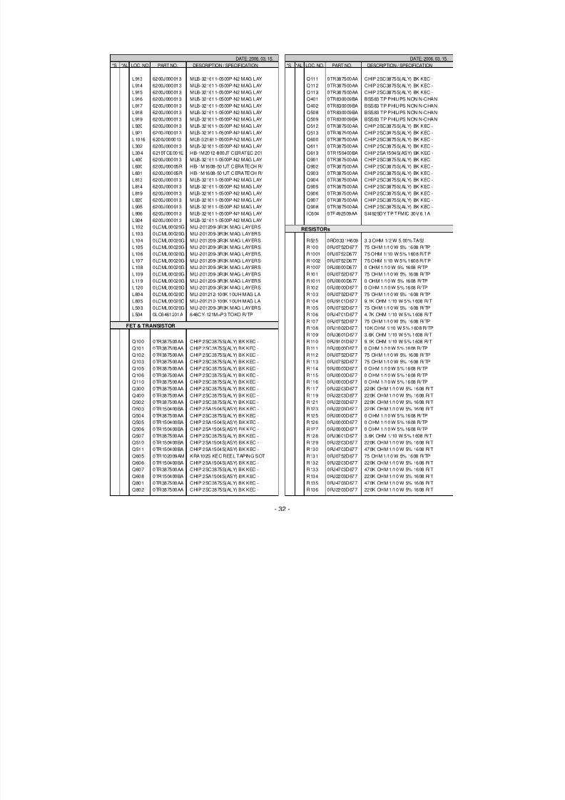
FET & TRANSISTOR
RESISTORs

7/22/2019 lg 32LC2R
http://slidepdf.com/reader/full/lg-32lc2r 33/40
DATE: 2006. 03. 15.
*S *AL LOC. NO. PART NO. DESCRIPTION / SPECIFICATION
R137 0RJ4703D677 470K OHM 1/10 W 5% 1608 R/T
R138 0RJ1001D677 1K OHM 1/10 W 5% 1608 R/TP
R139 0RJ1001D677 1K OHM 1/10 W 5% 1608 R/TP
R140 0RJ0000D677 0 OHM 1/10 W 5% 1608 R/TP
R141 0RJ4701D677 4.7K OHM 1/10 W 5% 1608 R/T
R142 0RJ1001D677 1K OHM 1/10 W 5% 1608 R/TP
R143 0RJ0000D677 0 OHM 1/10 W 5% 1608 R/TP
R144 0RJ1001D677 1K OHM 1/10 W 5% 1608 R/TP
R145 0RJ1001D677 1K OHM 1/10 W 5% 1608 R/TP
R146 0RJ1001D677 1K OHM 1/10 W 5% 1608 R/TP
R147 0RJ1001D677 1K OHM 1/10 W 5% 1608 R/TP
R148 0RJ1001D677 1K OHM 1/10 W 5% 1608 R/TP
R149 0RJ2000D677 200 OHM 1/10 W 5% 1608 R/TP
R150 0RJ0000D677 0 OHM 1/10 W 5% 1608 R/TP
R151 0RJ0000D677 0 OHM 1/10 W 5% 1608 R/TP
R152 0RJ0000D677 0 OHM 1/10 W 5% 1608 R/TP
R154 0RJ0000D677 0 OHM 1/10 W 5% 1608 R/TP
R159 0RJ2001D677 2K OHM 1/10 W 5% 1608 R/TP
R160 0RJ2001D677 2K OHM 1/10 W 5% 1608 R/TP
R161 0RJ6801D677 6800 OHM 1/10 W 5% 1608 R/T
R162 0RJ0000D677 0 OHM 1/10 W 5% 1608 R/TP
R163 0RJ4701D677 4.7K OHM 1/10 W 5% 1608 R/T
R164 0RJ2001D677 2K OHM 1/10 W 5% 1608 R/TP
R165 0RJ0822D677 82 OHM 1/10 W 5% 1608 R/TP
R166 0RJ0822D677 82 OHM 1/10 W 5% 1608 R/TP
R167 0RJ2700D677 270 OHM 1/10 W 5% 1608 R/TP
R168 0RJ2001D677 2K OHM 1/10 W 5% 1608 R/TP
R169 0RJ2700D677 270 OHM 1/10 W 5% 1608 R/TP
R171 0RJ0822D677 82 OHM 1/10 W 5% 1608 R/TP
R172 0RJ0822D677 82 OHM 1/10 W 5% 1608 R/TP
R179 0RJ2203D677 220K OHM 1/10 W 5% 1608 R/T
R180 0RJ2203D677 220K OHM 1/10 W 5% 1608 R/T
R181 0RJ0752D677 75 OHM 1/10 W 5% 1608 R/TP
R182 0RJ0752D677 75 OHM 1/10 W 5% 1608 R/TP
R183 0RJ0752D677 75 OHM 1/10 W 5% 1608 R/TPR185 0RJ2203D677 220K OHM 1/10 W 5% 1608 R/T
R186 0RJ1001D677 1K OHM 1/10 W 5% 1608 R/TP
R187 0RJ1001D677 1K OHM 1/10 W 5% 1608 R/TP
R188 0RJ0000D677 0 OHM 1/10 W 5% 1608 R/TP
R189 0RJ0000D677 0 OHM 1/10 W 5% 1608 R/TP
R190 0RJ0000D677 0 OHM 1/10 W 5% 1608 R/TP
R191 0RJ0752D677 75 OHM 1/10 W 5% 1608 R/TP
R197 0RJ2203D677 220K OHM 1/10 W 5% 1608 R/T
R199 0RJ0752D677 75 OHM 1/10 W 5% 1608 R/TP
R200 0RJ0000D677 0 OHM 1/10 W 5% 1608 R/TP
R201 0RJ1002D677 10K OHM 1/10 W 5% 1608 R/TP
R206 0RJ1002D677 10K OHM 1/10 W 5% 1608 R/TP
R208 0RJ0000D677 0 OHM 1/10 W 5% 1608 R/TP
R209 0RJ0000D677 0 OHM 1/10 W 5% 1608 R/TP
R212 0RJ2203D677 220K OHM 1/10 W 5% 1608 R/TR213 0RJ2203D677 220K OHM 1/10 W 5% 1608 R/T
R217 0RJ1001D677 1K OHM 1/10 W 5% 1608 R/TP
R218 0RJ1001D677 1K OHM 1/10 W 5% 1608 R/TP
R303 0RJ2203D677 220K OHM 1/10 W 5% 1608 R/T
R304 0RJ2203D677 220K OHM 1/10 W 5% 1608 R/T
R307 0RJ0752D677 75 OHM 1/10 W 5% 1608 R/TP
R308 0RJ1002D677 10K OHM 1/10 W 5% 1608 R/TP
R310 0RJ1001D677 1K OHM 1/10 W 5% 1608 R/TP
R311 0RJ1001D677 1K OHM 1/10 W 5% 1608 R/TP
R313 0RJ2001D677 2K OHM 1/10 W 5% 1608 R/TP
R314 0RJ0000D677 0 OHM 1/10 W 5% 1608 R/TP
R315 0RJ1002D677 10K OHM 1/10 W 5% 1608 R/TP
DATE: 2006. 03. 15.
*S *AL LOC. NO. PART NO. DESCRIPTION / SPECIFICATION
R316 0RJ0752D677 75 OHM 1/10 W 5% 1608 R/TP
R317 0RJ0000D677 0 OHM 1/10 W 5% 1608 R/TP
R320 0RJ0752D677 75 OHM 1/10 W 5% 1608 R/TP
R321 0RJ4701D677 4.7K OHM 1/10 W 5% 1608 R/T
R322 0RJ4701D677 4.7K OHM 1/10 W 5% 1608 R/T
R324 0RJ2001D677 2K OHM 1/10 W 5% 1608 R/TP
R325 0RJ3301D677 3.3K OHM 1/10 W 5% 1608 R/T
R326 0RJ0000D677 0 OHM 1/10 W 5% 1608 R/TP
R327 0RJ0000D677 0 OHM 1/10 W 5% 1608 R/TP
R328 0RJ0000D677 0 OHM 1/10 W 5% 1608 R/TP
R329 0RJ0000D677 0 OHM 1/10 W 5% 1608 R/TP
R330 0RJ1001D677 1K OHM 1/10 W 5% 1608 R/TP
R331 0RJ0000D677 0 OHM 1/10 W 5% 1608 R/TP
R332 0RJ1001D677 1K OHM 1/10 W 5% 1608 R/TP
R333 0RJ0000D677 0 OHM 1/10 W 5% 1608 R/TP
R334 0RJ0000D677 0 OHM 1/10 W 5% 1608 R/TP
R336 0RJ0000D677 0 OHM 1/10 W 5% 1608 R/TP
R337 0RJ0000D677 0 OHM 1/10 W 5% 1608 R/TP
R338 0RJ1000D677 100 OHM 1/10 W 5% 1608 R/TP
R339 0RJ1000D677 100 OHM 1/10 W 5% 1608 R/TP
R344 0RJ2002D677 20000 OHM 1/10 W 5% 1608 R/
R349 0RJ2202D677 22K OHM 1/10 W 5% 1608 R/TP
R350 0RJ2202D677 22K OHM 1/10 W 5% 1608 R/TP
R351 0RJ0000D677 0 OHM 1/10 W 5% 1608 R/TP
R352 0RJ0000D677 0 OHM 1/10 W 5% 1608 R/TP
R353 0RJ0000D677 0 OHM 1/10 W 5% 1608 R/TP
R354 0RJ0000D677 0 OHM 1/10 W 5% 1608 R/TP
R355 0RJ4700D677 470 OHM 1/10 W 5% 1608 R/TP
R358 0RJ0000D677 0 OHM 1/10 W 5% 1608 R/TP
R370 0RJ0000D677 0 OHM 1/10 W 5% 1608 R/TP
R372 0RJ1001D677 1K OHM 1/10 W 5% 1608 R/TP
R373 0RJ1001D677 1K OHM 1/10 W 5% 1608 R/TP
R402 0RJ1002D677 10K OHM 1/10 W 5% 1608 R/TP
R404 0RJ1001D677 1K OHM 1/10 W 5% 1608 R/TP
R405 0RJ1001D677 1K OHM 1/10 W 5% 1608 R/TPR417 0RJ4702D677 47000 OHM 1/10 W 5% 1608 R/
R418 0RJ4702D677 47000 OHM 1/10 W 5% 1608 R/
R423 0RJ1002D677 10K OHM 1/10 W 5% 1608 R/TP
R424 0RJ1002D677 10K OHM 1/10 W 5% 1608 R/TP
R502 0RJ1002D677 10K OHM 1/10 W 5% 1608 R/TP
R503 0RJ0222D677 22 OHM 1/10 W 5% 1608 R/TP
R506 0RJ1001D677 1K OHM 1/10 W 5% 1608 R/TP
R507 0RJ0000D677 0 OHM 1/10 W 5% 1608 R/TP
R508 0RJ2200D677 220 OHM 1/10 W 5% 1608 R/TP
R509 0RJ2200D677 220 OHM 1/10 W 5% 1608 R/TP
R510 0RJ4701D677 4.7K OHM 1/10 W 5% 1608 R/T
R511 0RJ4700D677 470 OHM 1/10 W 5% 1608 R/TP
R512 0RJ0822D677 82 OHM 1/10 W 5% 1608 R/TP
R513 0RJ0000D677 0 OHM 1/10 W 5% 1608 R/TP
R514 0RJ0000D677 0 OHM 1/10 W 5% 1608 R/TPR515 0RJ1000D677 100 OHM 1/10 W 5% 1608 R/TP
R516 0RJ1001D677 1K OHM 1/10 W 5% 1608 R/TP
R517 0RJ4701D677 4.7K OHM 1/10 W 5% 1608 R/T
R518 0RJ2000D677 200 OHM 1/10 W 5% 1608 R/TP
R521 0RJ1001D677 1K OHM 1/10 W 5% 1608 R/TP
R522 0RJ1500D677 150 OHM 1/10 W 5% 1608 R/TP
R524 0RJ1001D677 1K OHM 1/10 W 5% 1608 R/TP
R527 0RJ1001D677 1K OHM 1/10 W 5% 1608 R/TP
R529 0RJ1000D677 100 OHM 1/10 W 5% 1608 R/TP
R530 0RJ0472D677 47 OHM 1/10 W 5% 1608 R/TP
R531 0RJ1000D677 100 OHM 1/10 W 5% 1608 R/TP
R532 0RJ3002D677 30000 OHM 1/10 W 5% 1608 R/
- 33 -
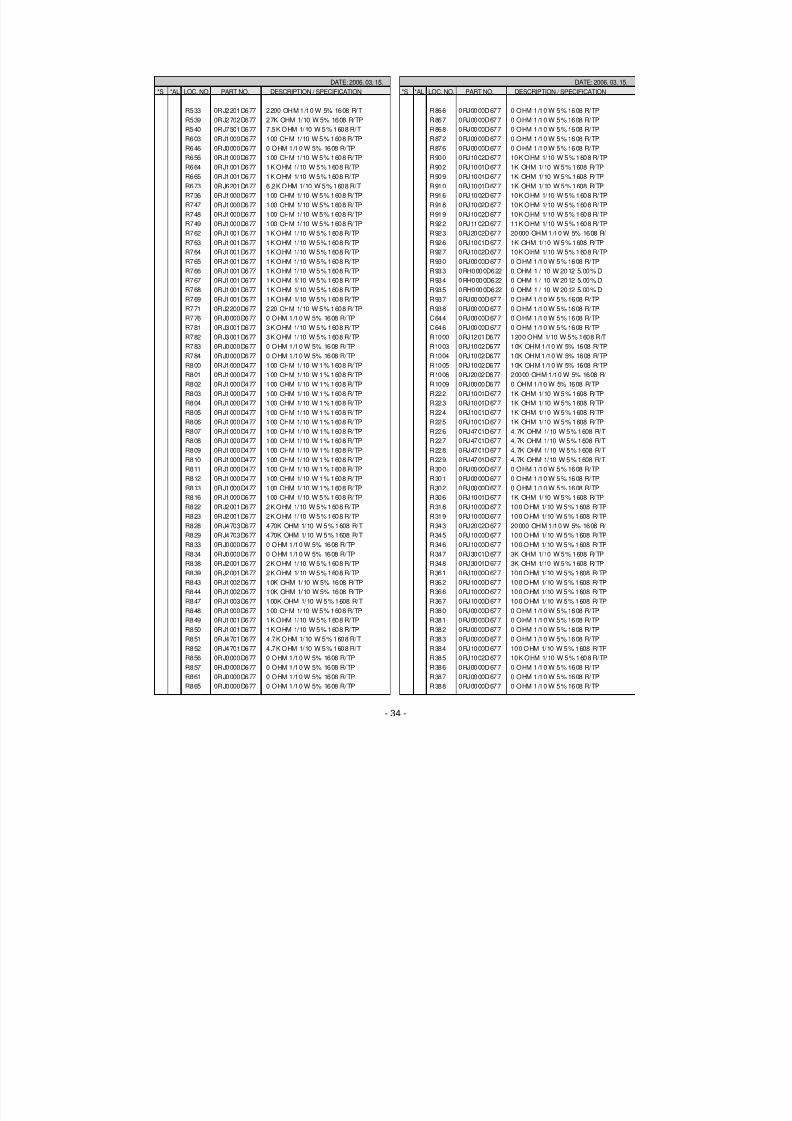
7/22/2019 lg 32LC2R
http://slidepdf.com/reader/full/lg-32lc2r 34/40
DATE: 2006. 03. 15.
*S *AL LOC. NO. PART NO. DESCRIPTION / SPECIFICATION
R533 0RJ2201D677 2200 OHM 1/10 W 5% 1608 R/T
R539 0RJ2702D677 27K OHM 1/10 W 5% 1608 R/TP
R540 0RJ7501D677 7.5K OHM 1/10 W 5% 1608 R/T
R603 0RJ1000D677 100 OHM 1/10 W 5% 1608 R/TP
R646 0RJ0000D677 0 OHM 1/10 W 5% 1608 R/TP
R656 0RJ1000D677 100 OHM 1/10 W 5% 1608 R/TP
R664 0RJ1001D677 1K OHM 1/10 W 5% 1608 R/TP
R665 0RJ1001D677 1K OHM 1/10 W 5% 1608 R/TP
R673 0RJ6201D677 6.2K OHM 1/10 W 5% 1608 R/T
R736 0RJ1000D677 100 OHM 1/10 W 5% 1608 R/TP
R747 0RJ1000D677 100 OHM 1/10 W 5% 1608 R/TP
R748 0RJ1000D677 100 OHM 1/10 W 5% 1608 R/TP
R749 0RJ1000D677 100 OHM 1/10 W 5% 1608 R/TP
R762 0RJ1001D677 1K OHM 1/10 W 5% 1608 R/TP
R763 0RJ1001D677 1K OHM 1/10 W 5% 1608 R/TP
R764 0RJ1001D677 1K OHM 1/10 W 5% 1608 R/TP
R765 0RJ1001D677 1K OHM 1/10 W 5% 1608 R/TP
R766 0RJ1001D677 1K OHM 1/10 W 5% 1608 R/TP
R767 0RJ1001D677 1K OHM 1/10 W 5% 1608 R/TP
R768 0RJ1001D677 1K OHM 1/10 W 5% 1608 R/TP
R769 0RJ1001D677 1K OHM 1/10 W 5% 1608 R/TP
R771 0RJ2200D677 220 OHM 1/10 W 5% 1608 R/TP
R776 0RJ0000D677 0 OHM 1/10 W 5% 1608 R/TP
R781 0RJ3001D677 3K OHM 1/10 W 5% 1608 R/TP
R782 0RJ3001D677 3K OHM 1/10 W 5% 1608 R/TP
R783 0RJ0000D677 0 OHM 1/10 W 5% 1608 R/TP
R784 0RJ0000D677 0 OHM 1/10 W 5% 1608 R/TP
R800 0RJ1000D477 100 OHM 1/10 W 1% 1608 R/TP
R801 0RJ1000D477 100 OHM 1/10 W 1% 1608 R/TP
R802 0RJ1000D477 100 OHM 1/10 W 1% 1608 R/TP
R803 0RJ1000D477 100 OHM 1/10 W 1% 1608 R/TP
R804 0RJ1000D477 100 OHM 1/10 W 1% 1608 R/TP
R805 0RJ1000D477 100 OHM 1/10 W 1% 1608 R/TP
R806 0RJ1000D477 100 OHM 1/10 W 1% 1608 R/TP
R807 0RJ1000D477 100 OHM 1/10 W 1% 1608 R/TPR808 0RJ1000D477 100 OHM 1/10 W 1% 1608 R/TP
R809 0RJ1000D477 100 OHM 1/10 W 1% 1608 R/TP
R810 0RJ1000D477 100 OHM 1/10 W 1% 1608 R/TP
R811 0RJ1000D477 100 OHM 1/10 W 1% 1608 R/TP
R812 0RJ1000D477 100 OHM 1/10 W 1% 1608 R/TP
R813 0RJ1000D477 100 OHM 1/10 W 1% 1608 R/TP
R816 0RJ1000D677 100 OHM 1/10 W 5% 1608 R/TP
R822 0RJ2001D677 2K OHM 1/10 W 5% 1608 R/TP
R823 0RJ2001D677 2K OHM 1/10 W 5% 1608 R/TP
R828 0RJ4703D677 470K OHM 1/10 W 5% 1608 R/T
R829 0RJ4703D677 470K OHM 1/10 W 5% 1608 R/T
R833 0RJ0000D677 0 OHM 1/10 W 5% 1608 R/TP
R834 0RJ0000D677 0 OHM 1/10 W 5% 1608 R/TP
R838 0RJ2001D677 2K OHM 1/10 W 5% 1608 R/TP
R839 0RJ2001D677 2K OHM 1/10 W 5% 1608 R/TPR843 0RJ1002D677 10K OHM 1/10 W 5% 1608 R/TP
R844 0RJ1002D677 10K OHM 1/10 W 5% 1608 R/TP
R847 0RJ1003D677 100K OHM 1/10 W 5% 1608 R/T
R848 0RJ1000D677 100 OHM 1/10 W 5% 1608 R/TP
R849 0RJ1001D677 1K OHM 1/10 W 5% 1608 R/TP
R850 0RJ1001D677 1K OHM 1/10 W 5% 1608 R/TP
R851 0RJ4701D677 4.7K OHM 1/10 W 5% 1608 R/T
R852 0RJ4701D677 4.7K OHM 1/10 W 5% 1608 R/T
R856 0RJ0000D677 0 OHM 1/10 W 5% 1608 R/TP
R857 0RJ0000D677 0 OHM 1/10 W 5% 1608 R/TP
R861 0RJ0000D677 0 OHM 1/10 W 5% 1608 R/TP
R865 0RJ0000D677 0 OHM 1/10 W 5% 1608 R/TP
DATE: 2006. 03. 15.
*S *AL LOC. NO. PART NO. DESCRIPTION / SPECIFICATION
R866 0RJ0000D677 0 OHM 1/10 W 5% 1608 R/TP
R867 0RJ0000D677 0 OHM 1/10 W 5% 1608 R/TP
R868 0RJ0000D677 0 OHM 1/10 W 5% 1608 R/TP
R872 0RJ0000D677 0 OHM 1/10 W 5% 1608 R/TP
R876 0RJ0000D677 0 OHM 1/10 W 5% 1608 R/TP
R900 0RJ1002D677 10K OHM 1/10 W 5% 1608 R/TP
R902 0RJ1001D677 1K OHM 1/10 W 5% 1608 R/TP
R909 0RJ1001D677 1K OHM 1/10 W 5% 1608 R/TP
R910 0RJ1001D677 1K OHM 1/10 W 5% 1608 R/TP
R916 0RJ1002D677 10K OHM 1/10 W 5% 1608 R/TP
R918 0RJ1002D677 10K OHM 1/10 W 5% 1608 R/TP
R919 0RJ1002D677 10K OHM 1/10 W 5% 1608 R/TP
R922 0RJ1102D677 11K OHM 1/10 W 5% 1608 R/TP
R923 0RJ2002D677 20000 OHM 1/10 W 5% 1608 R/
R926 0RJ1001D677 1K OHM 1/10 W 5% 1608 R/TP
R927 0RJ1002D677 10K OHM 1/10 W 5% 1608 R/TP
R930 0RJ0000D677 0 OHM 1/10 W 5% 1608 R/TP
R933 0RH0000D622 0 OHM 1 / 10 W 2012 5.00% D
R934 0RH0000D622 0 OHM 1 / 10 W 2012 5.00% D
R935 0RH0000D622 0 OHM 1 / 10 W 2012 5.00% D
R937 0RJ0000D677 0 OHM 1/10 W 5% 1608 R/TP
R938 0RJ0000D677 0 OHM 1/10 W 5% 1608 R/TP
C644 0RJ0000D677 0 OHM 1/10 W 5% 1608 R/TP
C646 0RJ0000D677 0 OHM 1/10 W 5% 1608 R/TP
R1000 0RJ1201D677 1200 OHM 1/10 W 5% 1608 R/T
R1003 0RJ1002D677 10K OHM 1/10 W 5% 1608 R/TP
R1004 0RJ1002D677 10K OHM 1/10 W 5% 1608 R/TP
R1005 0RJ1002D677 10K OHM 1/10 W 5% 1608 R/TP
R1006 0RJ2002D677 20000 OHM 1/10 W 5% 1608 R/
R1009 0RJ0000D677 0 OHM 1/10 W 5% 1608 R/TP
R222 0RJ1001D677 1K OHM 1/10 W 5% 1608 R/TP
R223 0RJ1001D677 1K OHM 1/10 W 5% 1608 R/TP
R224 0RJ1001D677 1K OHM 1/10 W 5% 1608 R/TP
R225 0RJ1001D677 1K OHM 1/10 W 5% 1608 R/TP
R226 0RJ4701D677 4.7K OHM 1/10 W 5% 1608 R/TR227 0RJ4701D677 4.7K OHM 1/10 W 5% 1608 R/T
R228 0RJ4701D677 4.7K OHM 1/10 W 5% 1608 R/T
R229 0RJ4701D677 4.7K OHM 1/10 W 5% 1608 R/T
R300 0RJ0000D677 0 OHM 1/10 W 5% 1608 R/TP
R301 0RJ0000D677 0 OHM 1/10 W 5% 1608 R/TP
R302 0RJ0000D677 0 OHM 1/10 W 5% 1608 R/TP
R306 0RJ1001D677 1K OHM 1/10 W 5% 1608 R/TP
R318 0RJ1000D677 100 OHM 1/10 W 5% 1608 R/TP
R319 0RJ1000D677 100 OHM 1/10 W 5% 1608 R/TP
R343 0RJ2002D677 20000 OHM 1/10 W 5% 1608 R/
R345 0RJ1000D677 100 OHM 1/10 W 5% 1608 R/TP
R346 0RJ1000D677 100 OHM 1/10 W 5% 1608 R/TP
R347 0RJ3001D677 3K OHM 1/10 W 5% 1608 R/TP
R348 0RJ3001D677 3K OHM 1/10 W 5% 1608 R/TP
R361 0RJ1000D677 100 OHM 1/10 W 5% 1608 R/TPR362 0RJ1000D677 100 OHM 1/10 W 5% 1608 R/TP
R366 0RJ1000D677 100 OHM 1/10 W 5% 1608 R/TP
R367 0RJ1000D677 100 OHM 1/10 W 5% 1608 R/TP
R380 0RJ0000D677 0 OHM 1/10 W 5% 1608 R/TP
R381 0RJ0000D677 0 OHM 1/10 W 5% 1608 R/TP
R382 0RJ0000D677 0 OHM 1/10 W 5% 1608 R/TP
R383 0RJ0000D677 0 OHM 1/10 W 5% 1608 R/TP
R384 0RJ1000D677 100 OHM 1/10 W 5% 1608 R/TP
R385 0RJ1002D677 10K OHM 1/10 W 5% 1608 R/TP
R386 0RJ0000D677 0 OHM 1/10 W 5% 1608 R/TP
R387 0RJ0000D677 0 OHM 1/10 W 5% 1608 R/TP
R388 0RJ0000D677 0 OHM 1/10 W 5% 1608 R/TP
- 34 -

7/22/2019 lg 32LC2R
http://slidepdf.com/reader/full/lg-32lc2r 35/40
DATE: 2006. 03. 15.
*S *AL LOC. NO. PART NO. DESCRIPTION / SPECIFICATION
R401 0RJ0000D677 0 OHM 1/10 W 5% 1608 R/TP
R406 0RJ1000D677 100 OHM 1/10 W 5% 1608 R/TP
R407 0RJ1000D677 100 OHM 1/10 W 5% 1608 R/TP
R421 0RJ1000D677 100 OHM 1/10 W 5% 1608 R/TP
R422 0RJ1000D677 100 OHM 1/10 W 5% 1608 R/TP
R425 0RJ4990D477 499 OHM 1/10 W 1% 1608 R/TP
R426 0RJ0222D677 22 OHM 1/10 W 5% 1608 R/TP
R427 0RJ0222D677 22 OHM 1/10 W 5% 1608 R/TP
R428 0RJ0222D677 22 OHM 1/10 W 5% 1608 R/TP
R433 0RJ1000D677 100 OHM 1/10 W 5% 1608 R/TP
R434 0RJ1000D677 100 OHM 1/10 W 5% 1608 R/TP
R435 0RJ0222D677 22 OHM 1/10 W 5% 1608 R/TP
R436 0RJ0222D677 22 OHM 1/10 W 5% 1608 R/TP
R437 0RJ0222D677 22 OHM 1/10 W 5% 1608 R/TP
R438 0RJ0222D677 22 OHM 1/10 W 5% 1608 R/TP
R441 0RJ1002D677 10K OHM 1/10 W 5% 1608 R/TP
R442 0RJ1002D677 10K OHM 1/10 W 5% 1608 R/TP
R451 0RJ1501D677 1.5K OHM 1/10 W 5% 1608 R/T
R519 0RJ2700D677 270 OHM 1/10 W 5% 1608 R/TP
R520 0RJ2200D677 220 OHM 1/10 W 5% 1608 R/TP
R523 0RJ4701D677 4.7K OHM 1/10 W 5% 1608 R/T
R526 0RJ4701D677 4.7K OHM 1/10 W 5% 1608 R/T
R528 0RJ1800D677 180 OHM 1/10 W 5% 1608 R/TP
R534 0RJ1001D677 1K OHM 1/10 W 5% 1608 R/TP
R535 0RJ4702D677 47000 OHM 1/10 W 5% 1608 R/
R536 0RJ1001D677 1K OHM 1/10 W 5% 1608 R/TP
R600 0RJ0000D677 0 OHM 1/10 W 5% 1608 R/TP
R601 0RJ1000D677 100 OHM 1/10 W 5% 1608 R/TP
R604 0RJ1001D677 1K OHM 1/10 W 5% 1608 R/TP
R607 0RJ1002D677 10K OHM 1/10 W 5% 1608 R/TP
R620 0RJ1000D677 100 OHM 1/10 W 5% 1608 R/TP
R621 0RJ0000D677 0 OHM 1/10 W 5% 1608 R/TP
R622 0RJ0000D677 0 OHM 1/10 W 5% 1608 R/TP
R623 0RJ0000D677 0 OHM 1/10 W 5% 1608 R/TP
R624 0RJ0000D677 0 OHM 1/10 W 5% 1608 R/TPR627 0RJ0000D677 0 OHM 1/10 W 5% 1608 R/TP
R628 0RJ0000D677 0 OHM 1/10 W 5% 1608 R/TP
R629 0RJ1500D677 150 OHM 1/10 W 5% 1608 R/TP
R630 0RJ4700D677 470 OHM 1/10 W 5% 1608 R/TP
R631 0RJ1500D677 150 OHM 1/10 W 5% 1608 R/TP
R632 0RJ1802D677 18K OHM 1/10 W 5% 1608 R/TP
R633 0RJ1000D677 100 OHM 1/10 W 5% 1608 R/TP
R634 0RJ1000D677 100 OHM 1/10 W 5% 1608 R/TP
R635 0RJ1000D677 100 OHM 1/10 W 5% 1608 R/TP
R636 0RJ1000D677 100 OHM 1/10 W 5% 1608 R/TP
R637 0RJ1000D677 100 OHM 1/10 W 5% 1608 R/TP
R638 0RJ1001D677 1K OHM 1/10 W 5% 1608 R/TP
R640 0RJ1000D677 100 OHM 1/10 W 5% 1608 R/TP
R645 0RJ1000D677 100 OHM 1/10 W 5% 1608 R/TP
R647 0RJ1002D677 10K OHM 1/10 W 5% 1608 R/TPR648 0RJ1002D677 10K OHM 1/10 W 5% 1608 R/TP
R649 0RJ1002D677 10K OHM 1/10 W 5% 1608 R/TP
R650 0RJ1002D677 10K OHM 1/10 W 5% 1608 R/TP
R651 0RJ1002D677 10K OHM 1/10 W 5% 1608 R/TP
R652 0RJ1002D677 10K OHM 1/10 W 5% 1608 R/TP
R653 0RJ1000D677 100 OHM 1/10 W 5% 1608 R/TP
R654 0RJ1000D677 100 OHM 1/10 W 5% 1608 R/TP
R660 0RJ8201D677 8.2K OHM 1/10 W 5% 1608 R/T
R662 0RJ1002D677 10K OHM 1/10 W 5% 1608 R/TP
R663 0RJ1002D677 10K OHM 1/10 W 5% 1608 R/TP
R666 0RJ4701D677 4.7K OHM 1/10 W 5% 1608 R/T
R667 0RJ1000D677 100 OHM 1/10 W 5% 1608 R/TP
DATE: 2006. 03. 15.
*S *AL LOC. NO. PART NO. DESCRIPTION / SPECIFICATION
R668 0RJ1000D677 100 OHM 1/10 W 5% 1608 R/TP
R670 0RJ1000D677 100 OHM 1/10 W 5% 1608 R/TP
R671 0RJ4701D677 4.7K OHM 1/10 W 5% 1608 R/T
R672 0RJ1000D677 100 OHM 1/10 W 5% 1608 R/TP
R675 0RJ1000D677 100 OHM 1/10 W 5% 1608 R/TP
R676 0RJ1000D677 100 OHM 1/10 W 5% 1608 R/TP
R677 0RJ1000D677 100 OHM 1/10 W 5% 1608 R/TP
R678 0RJ1000D677 100 OHM 1/10 W 5% 1608 R/TP
R679 0RJ1000D677 100 OHM 1/10 W 5% 1608 R/TP
R680 0RJ1000D677 100 OHM 1/10 W 5% 1608 R/TP
R681 0RJ2001D677 2K OHM 1/10 W 5% 1608 R/TP
R686 0RJ1000D677 100 OHM 1/10 W 5% 1608 R/TP
R687 0RJ1000D677 100 OHM 1/10 W 5% 1608 R/TP
R689 0RJ2200D677 220 OHM 1/10 W 5% 1608 R/TP
R690 0RJ1000D677 100 OHM 1/10 W 5% 1608 R/TP
R691 0RJ2200D677 220 OHM 1/10 W 5% 1608 R/TP
R692 0RJ1000D677 100 OHM 1/10 W 5% 1608 R/TP
R693 0RJ2200D677 220 OHM 1/10 W 5% 1608 R/TP
R694 0RJ1000D677 100 OHM 1/10 W 5% 1608 R/TP
R695 0RJ0222D677 22 OHM 1/10 W 5% 1608 R/TP
R697 0RJ2001D677 2K OHM 1/10 W 5% 1608 R/TP
R699 0RJ1000D677 100 OHM 1/10 W 5% 1608 R/TP
R700 0RJ1000D677 100 OHM 1/10 W 5% 1608 R/TP
R702 0RJ1000D677 100 OHM 1/10 W 5% 1608 R/TP
R703 0RJ1000D677 100 OHM 1/10 W 5% 1608 R/TP
R704 0RJ6202D677 62K OHM 1/10 W 5% 1608 R/TP
R705 0RJ2402D677 24K OHM 1/10 W 5% 1608 R/TP
R708 0RJ1501D677 1.5K OHM 1/10 W 5% 1608 R/T
R709 0RJ4700D677 470 OHM 1/10 W 5% 1608 R/TP
R711 0RJ0222D677 22 OHM 1/10 W 5% 1608 R/TP
R712 0RJ0222D677 22 OHM 1/10 W 5% 1608 R/TP
R713 0RJ0222D677 22 OHM 1/10 W 5% 1608 R/TP
R714 0RJ2200D677 220 OHM 1/10 W 5% 1608 R/TP
R715 0RJ2200D677 220 OHM 1/10 W 5% 1608 R/TP
R718 0RJ4701D677 4.7K OHM 1/10 W 5% 1608 R/TR721 0RJ4701D677 4.7K OHM 1/10 W 5% 1608 R/T
R728 0RJ1000D677 100 OHM 1/10 W 5% 1608 R/TP
R729 0RJ1000D677 100 OHM 1/10 W 5% 1608 R/TP
R730 0RJ1000D677 100 OHM 1/10 W 5% 1608 R/TP
R732 0RJ1000D677 100 OHM 1/10 W 5% 1608 R/TP
R733 0RJ1000D677 100 OHM 1/10 W 5% 1608 R/TP
R734 0RJ1000D677 100 OHM 1/10 W 5% 1608 R/TP
R735 0RJ0000D677 0 OHM 1/10 W 5% 1608 R/TP
R737 0RJ1000D677 100 OHM 1/10 W 5% 1608 R/TP
R738 0RJ0000D677 0 OHM 1/10 W 5% 1608 R/TP
R742 0RJ6201D677 6.2K OHM 1/10 W 5% 1608 R/T
R744 0RJ1001D677 1K OHM 1/10 W 5% 1608 R/TP
R750 0RJ0000D677 0 OHM 1/10 W 5% 1608 R/TP
R751 0RJ1000D677 100 OHM 1/10 W 5% 1608 R/TP
R752 0RJ1000D677 100 OHM 1/10 W 5% 1608 R/TPR753 0RJ1000D677 100 OHM 1/10 W 5% 1608 R/TP
R756 0RJ1000D677 100 OHM 1/10 W 5% 1608 R/TP
R757 0RJ1000D677 100 OHM 1/10 W 5% 1608 R/TP
R758 0RJ1001D677 1K OHM 1/10 W 5% 1608 R/TP
R759 0RJ1001D677 1K OHM 1/10 W 5% 1608 R/TP
R760 0RJ1001D677 1K OHM 1/10 W 5% 1608 R/TP
R761 0RJ1001D677 1K OHM 1/10 W 5% 1608 R/TP
R772 0RJ2200D677 220 OHM 1/10 W 5% 1608 R/TP
R778 0RJ0000D677 0 OHM 1/10 W 5% 1608 R/TP
R780 0RJ0000D677 0 OHM 1/10 W 5% 1608 R/TP
R855 0RJ0000D677 0 OHM 1/10 W 5% 1608 R/TP
R858 0RJ0000D677 0 OHM 1/10 W 5% 1608 R/TP
- 35 -
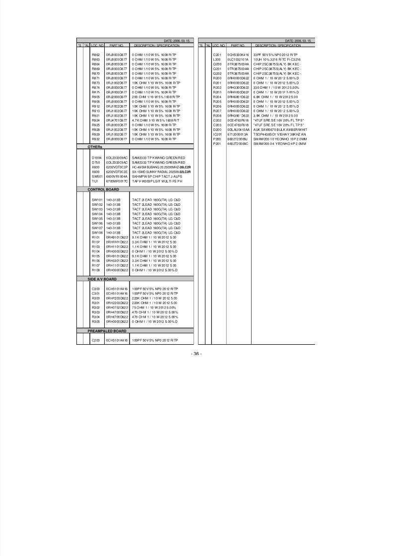
7/22/2019 lg 32LC2R
http://slidepdf.com/reader/full/lg-32lc2r 36/40
DATE: 2006. 03. 15.
*S *AL LOC. NO. PART NO. DESCRIPTION / SPECIFICATION
R862 0RJ0000D677 0 OHM 1/10 W 5% 1608 R/TP
R863 0RJ0000D677 0 OHM 1/10 W 5% 1608 R/TP
R864 0RJ0000D677 0 OHM 1/10 W 5% 1608 R/TP
R869 0RJ0000D677 0 OHM 1/10 W 5% 1608 R/TP
R870 0RJ0000D677 0 OHM 1/10 W 5% 1608 R/TP
R871 0RJ0000D677 0 OHM 1/10 W 5% 1608 R/TP
R873 0RJ1002D677 10K OHM 1/10 W 5% 1608 R/TP
R874 0RJ0000D677 0 OHM 1/10 W 5% 1608 R/TP
R875 0RJ0000D677 0 OHM 1/10 W 5% 1608 R/TP
R905 0RJ2000D677 200 OHM 1/10 W 5% 1608 R/TP
R906 0RJ0000D677 0 OHM 1/10 W 5% 1608 R/TP
R912 0RJ1002D677 10K OHM 1/10 W 5% 1608 R/TP
R913 0RJ1002D677 10K OHM 1/10 W 5% 1608 R/TP
R921 0RJ1002D677 10K OHM 1/10 W 5% 1608 R/TP
R924 0RJ4701D677 4.7K OHM 1/10 W 5% 1608 R/T
R925 0RJ0000D677 0 OHM 1/10 W 5% 1608 R/TP
R928 0RJ1002D677 10K OHM 1/10 W 5% 1608 R/TP
R929 0RJ1002D677 10K OHM 1/10 W 5% 1608 R/TP
R932 0RJ0000D677 0 OHM 1/10 W 5% 1608 R/TP
D1004 0DL233309AC SAM2333 TP KWANG GREEN/RED
D750 0DL233309AC SAM2333 TP KWANG GREEN/RED
X600 6202VDT002P HC-49/SM BUBANG 20.25000MHZ-26LC2R
X600 6202VDT002E SX-1SMD SUNNY RADIAL 202500-32LC2R
SW501 6600VR1004A SKHMPW 5P CHIP TACT J-ALPS
TU1 6700MF0017C TAFV-W303P LGIT MULTI FS PH
SW101 140-313B TACT 2LEAD 160G(TA) LG C&D
SW102 140-313B TACT 2LEAD 160G(TA) LG C&D
SW103 140-313B TACT 2LEAD 160G(TA) LG C&D
SW104 140-313B TACT 2LEAD 160G(TA) LG C&DSW105 140-313B TACT 2LEAD 160G(TA) LG C&D
SW106 140-313B TACT 2LEAD 160G(TA) LG C&D
SW107 140-313B TACT 2LEAD 160G(TA) LG C&D
SW108 140-313B TACT 2LEAD 160G(TA) LG C&D
R101 0RH9101D622 9.1K OHM 1 / 10 W 2012 5.00
R102 0RH3301D622 3.3K OHM 1 / 10 W 2012 5.00
R103 0RH1101D622 1.1K OHM 1 / 10 W 2012 5.00
R104 0RH0000D622 0 OHM 1 / 10 W 2012 5.00% D
R105 0RH9101D622 9.1K OHM 1 / 10 W 2012 5.00
R106 0RH3301D622 3.3K OHM 1 / 10 W 2012 5.00
R107 0RH1101D622 1.1K OHM 1 / 10 W 2012 5.00
R108 0RH0000D622 0 OHM 1 / 10 W 2012 5.00% D
C300 0CH5101K416 100PF 50V 5% NP0 2012 R/TP
C301 0CH5101K416 100PF 50V 5% NP0 2012 R/TP
R300 0RH2203D622 220K OHM 1 / 10 W 2012 5.00
R301 0RH2203D622 220K OHM 1 / 10 W 2012 5.00
R302 0RH0752D622 75 OHM 1 / 10 W 2012 5.00%
R303 0RH4700D622 470 OHM 1 / 10 W 2012 5.00%
R304 0RH4700D622 470 OHM 1 / 10 W 2012 5.00%
R305 0RH0000D622 0 OHM 1 / 10 W 2012 5.00% D
C200 0CH5101K416 100PF 50V 5% NP0 2012 R/TP
DATE: 2006. 03. 15.
*S *AL LOC. NO. PART NO. DESCRIPTION / SPECIFICATION
C201 0CH5330K416 33PF 50V 5% NP0 2012 R/TP
L200 0LC1032101A 10UH 10% 3216 R/TC FI-C3216
Q200 0TR387500AA CHIP 2SC3875S(ALY) BK KEC -
Q201 0TR387500AA CHIP 2SC3875S(ALY) BK KEC -
Q202 0TR387500AA CHIP 2SC3875S(ALY) BK KEC -
R200 0RH0000D622 0 OHM 1 / 10 W 2012 5.00% D
R201 0RH0000D622 0 OHM 1 / 10 W 2012 5.00% D
R202 0RH3300D622 330 OHM 1 / 10 W 2012 5.00%
R203 0RH0000D622 0 OHM 1 / 10 W 2012 5.00% D
R204 0RH6801D622 6.8K OHM 1 / 10 W 2012 5.00
R205 0RH0000D622 0 OHM 1 / 10 W 2012 5.00% D
R206 0RH0000D622 0 OHM 1 / 10 W 2012 5.00% D
R207 0RH0000D622 0 OHM 1 / 10 W 2012 5.00% D
R208 0RH3901D622 3.9K OHM 1 / 10 W 2012 5.00
C202 0CE4763F618 "47UF SRE,SE 16V 20% FL TP 5"
C203 0CE4763F618 "47UF SRE,SE 16V 20% FL TP 5"
D200 0DLAU0410AA AUK SAW5670 BULK AMBER/WHIT
IC201 6712000013A TSOP4438SO1 VISHAY 38KHZ AN
P200 6602T20009J SMAW200-10 YEONHO 10P 2.0MM
P201 6602T20009C SMAW200-04 YEONHO 4P 2.0MM
- 36 -
OTHERs
CONTROL BOARD
SIDE A/V BOARD
PREAMP&LED BOARD

7/22/2019 lg 32LC2R
http://slidepdf.com/reader/full/lg-32lc2r 37/40

7/22/2019 lg 32LC2R
http://slidepdf.com/reader/full/lg-32lc2r 38/40

7/22/2019 lg 32LC2R
http://slidepdf.com/reader/full/lg-32lc2r 39/40
7/22/2019 lg 32LC2R
http://slidepdf.com/reader/full/lg-32lc2r 40/40
Jan., 2006Printed in KoreaP/NO : MFL30105502