lesson-2: 8051 io ports, circuits and io programming and external
TRANSCRIPT

2008 Chapter-2 L2: "Embedded Systems - Architecture, Programming and Design" , Raj Kamal, Publs.: McGraw-Hill Education 1
8051 AND ADVANCED PROCESSOR
ARCHITECTURES –Lesson-2: 8051 IO ports, Circuits and IO Programming and External
Memory Circuits

2008 Chapter-2 L2: "Embedded Systems - Architecture, Programming and Design" , Raj Kamal, Publs.: McGraw-Hill Education 2
1.1. IO PORTSIO PORTS

2008 Chapter-2 L2: "Embedded Systems - Architecture, Programming and Design" , Raj Kamal, Publs.: McGraw-Hill Education 3
Ports P0 and P1 pins and alternative functionsPorts P0 and P1 pins and alternative functions
P1.0 P1.1 P1.2 P1.3 P1.4 P1.5 P1.6 P1.7 Also P1.6 as I2C clock, P1.7 as I2C serial data, and P1.0 and P1.1 for T2 (8052)
P0 P1
P0.0 P0.1 P0.2 P0.3 P0.4 P0.5 P0.6 P0.7 Also as AD0- AD7
Lower address bits cum data bus

2008 Chapter-2 L2: "Embedded Systems - Architecture, Programming and Design" , Raj Kamal, Publs.: McGraw-Hill Education 4
Ports P2 and P3 pins and alternative functionsPorts P2 and P3 pins and alternative functions
P3.0 P3.1 P3.2 P3.3 P3.4 P3.5 P3.6 P3.7 Also RxD/SyncData, TxD/SyncClk, INT0/GT0, INT1/GT1, T0, T1, WR, RD
P2 P3
P2.0 P2.1 P2.2 P2.3 P2.4 P2.5 P2.6 P2.7 Also as A8- A15
Higher address-bits bus

2008 Chapter-2 L2: "Embedded Systems - Architecture, Programming and Design" , Raj Kamal, Publs.: McGraw-Hill Education 5
2.2. IO CircuitsIO Circuits

2008 Chapter-2 L2: "Embedded Systems - Architecture, Programming and Design" , Raj Kamal, Publs.: McGraw-Hill Education 6
IO port circuit for two stepper motors in IO port circuit for two stepper motors in a printera printer
P1.0
P1.1
P1.2
P1.3
PrinterCoil A
Coil B
Coil C
Coil D
Stepper Motor 1 Stepper Motor 2
P1.4
P1.5
P1.6
P1.7
Coil A’
Coil B’
Coil C’
Coil D’

2008 Chapter-2 L2: "Embedded Systems - Architecture, Programming and Design" , Raj Kamal, Publs.: McGraw-Hill Education 7
IO port circuit for six servo motors IO port circuit for six servo motors in a robot in a robot
P1.0 P1.1P1.2 P1.3P1.4 P1.5
Servomotor0 Servomotor1Servomotor2 Servomotor3Servomotor4 Servomotor5

2008 Chapter-2 L2: "Embedded Systems - Architecture, Programming and Design" , Raj Kamal, Publs.: McGraw-Hill Education 8
3.3. IO Byte ProgrammingIO Byte Programming

2008 Chapter-2 L2: "Embedded Systems - Architecture, Programming and Design" , Raj Kamal, Publs.: McGraw-Hill Education 9
� 8051 internal IO ports P0, P1, P2 and P3 byte addresses used to access and perform read or write or other operations
� Direct 8-bit addresses of each are specified in the instructions
� Addresses of bytes at P0, P1, P2 and P3─0x80, 0x90, 0xA0 and 0xB0.
Port Byte ProgrammingPort Byte Programming

2008 Chapter-2 L2: "Embedded Systems - Architecture, Programming and Design" , Raj Kamal, Publs.: McGraw-Hill Education 10
� MOV 0xA0, #0xFF moves bits to port P2 and P2 bits will become = 11111111b.
� MOV 0x90, #0x1C moves bits at port P1 = 00011100b.
� After this instruction, INC 0x90 will make P1 = 00011100b + 1 = 00011101b.
Example 2.1Example 2.1

2008 Chapter-2 L2: "Embedded Systems - Architecture, Programming and Design" , Raj Kamal, Publs.: McGraw-Hill Education 11
4.4. IO Bit ProgrammingIO Bit Programming

2008 Chapter-2 L2: "Embedded Systems - Architecture, Programming and Design" , Raj Kamal, Publs.: McGraw-Hill Education 12
� Each port P0, P1, P2 and P3 8 bits and each bit has addresses to access and perform read or write or other operations using bit-manipulation instructions.
� Addresses are the bit addresses. Each bit addressis of 8-bits, which are specified in the instructions.
� Bits P0.0 to P0.7 addresses ─ 0x80 to 0x87. � Bits P1.0 to P1.7 addresses ─ 0x90 to 0x97, � P2.0 to P2.7 ─ 0xA0 to 0xA7 and � P3.0 to P3.7 ─ 0xB0 to 0xB7.
Bit ProgrammingBit Programming

2008 Chapter-2 L2: "Embedded Systems - Architecture, Programming and Design" , Raj Kamal, Publs.: McGraw-Hill Education 13
� All instructions in the instruction set using bit addresses can be used to access and perform complement read or write or other operations.
� C flag in PSW ─ Accumulator for bit logic operations.
Bit ProgrammingBit Programming

2008 Chapter-2 L2: "Embedded Systems - Architecture, Programming and Design" , Raj Kamal, Publs.: McGraw-Hill Education 14
� CPL 0x90 complements the bit 0 at port P1.
� CLR 0x80 makes P0.0 as 0. Now after a delay of period= T1, the SETB 0x80 will make P0.0 as 1. Now after a delay of period= T2, the CLRB 0x80 will make gain P0.0 as 0.
A pulse of time-period T2 and duty cycle 100 ×T1/(T1 + T2) creates if the instructions are executed in a loop.
Example 2.2Example 2.2

2008 Chapter-2 L2: "Embedded Systems - Architecture, Programming and Design" , Raj Kamal, Publs.: McGraw-Hill Education 15
� SETB C will set carry bit in PSW to 1. After this operation, ANL C, 0x93 will perform logic AND operation between bits C and P1.3 and result will be in C. If P1.3 = 0 then C will become 0 else C will remain 1.
� CLR C will reset (clear) carry bit in PSW to 0. After this operation, ORL C, 0xB2 will perform logic OR operation between bits C and P3.2 and result will be in C. If P3.2 = 0 then C will remain 0 else C will remain 1. After this operation, MOV 0x85, C will move result in C to P0.5.
Example 2.2 (contd.) Example 2.2 (contd.)

2008 Chapter-2 L2: "Embedded Systems - Architecture, Programming and Design" , Raj Kamal, Publs.: McGraw-Hill Education 16
5. External Memory and Port Circuits

2008 Chapter-2 L2: "Embedded Systems - Architecture, Programming and Design" , Raj Kamal, Publs.: McGraw-Hill Education 17
Memory mapped IOMemory mapped IO
� 8051 Memory and ports assigned the addresses such each have distinct range of addresses in the data memory address space.
� Interfacing circuit design identical to that for the memory connects the external ports and programmable peripheral interface (PPI).

2008 Chapter-2 L2: "Embedded Systems - Architecture, Programming and Design" , Raj Kamal, Publs.: McGraw-Hill Education 18
Connection to the external program and data memory circuits
PSEN
P3.7 (RD)
ALE
P3.6 (WR)
EA
AD0-AD7
Latch P0 as AD0-AD7
P2 as A8-A15
Program Memory0x0000-0xFFFF
D0-D7
Latch
A0- A7
Data Memory0x0000-0xFFFF
A0- A7
A8- A15
A8- A15
D0- D7
D0- D7

2008 Chapter-2 L2: "Embedded Systems - Architecture, Programming and Design" , Raj Kamal, Publs.: McGraw-Hill Education 19
Interfacing using external PPI port in 8051Interfacing using external PPI port in 8051
P0 as AD0-AD7
P2 as A8-A15
8255Decoder
A8- A15
A2- A7
P3.7 (RD)
P3.6 (WR)
Latch
AD0-AD7 A15
A0A1
ALE
PA
PB
PC
[A1] New Figure 2.4 in this Edition – Author

2008 Chapter-2 L2: "Embedded Systems - Architecture, Programming and Design" , Raj Kamal, Publs.: McGraw-Hill Education 20
Port P0 used in expanded mode and ALE
� AD0-AD7 the multiplexed signals of A0-A7 lower address bits of the address bus and D0-D7 bits of data bus.
� A0-A7 and D0-D7 time division multiplexed. For an interval, the processor activates ALE (address latch enable) in an instruction cycle and the AD0-AD7 lines have A0-A7 and a latch circuit separates A0-A7 signals for the memory
2008 Chapter-2 L2: "Embedded Systems - Architecture, Programming and Design" , Raj Kamal, Publs.: McGraw-Hill Education 21
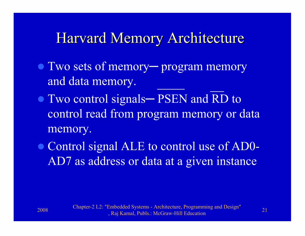
Harvard Memory ArchitectureHarvard Memory Architecture
� Two sets of memory─ program memory and data memory.
� Two control signals─ PSEN and RD to control read from program memory or data memory.
� Control signal ALE to control use of AD0-AD7 as address or data at a given instance

2008 Chapter-2 L2: "Embedded Systems - Architecture, Programming and Design" , Raj Kamal, Publs.: McGraw-Hill Education 22
Port P2 expanded mode, PSEN and RDPort P2 expanded mode, PSEN and RD
� A8-A15 address signals ─� When the processor activates PSEN
(Program store enable), it reads the byte from external program memory through D0-D7 data bus.
� When the processor activates RD (read), it reads the byte from external data memory through D0-D7 data bus.

2008 Chapter-2 L2: "Embedded Systems - Architecture, Programming and Design" , Raj Kamal, Publs.: McGraw-Hill Education 23
Addresses outside the internal RAM, Addresses outside the internal RAM, SFR and internal program memory when SFR and internal program memory when
control signal EA inactivecontrol signal EA inactive
� Then processor always accesses the external memory whether EA active or not .
� Internal RAM and SFR addresses between 0x00 and 0xFF are same as external data memory addresses 0x0000 and 0xFFFF.
� Internal program memory addresses between 0x0000 to 0xFFF (in case of 4 kB internal ROM) are same as external program memory addresses 0x0000 and 0xFFFF.

2008 Chapter-2 L2: "Embedded Systems - Architecture, Programming and Design" , Raj Kamal, Publs.: McGraw-Hill Education 24
Control signal EAControl signal EA
� When a control signal EA activate ─processor always accesses the external addresses in memory instead of internal memory or register addresses

2008 Chapter-2 L2: "Embedded Systems - Architecture, Programming and Design" , Raj Kamal, Publs.: McGraw-Hill Education 25
SummarySummary

2008 Chapter-2 L2: "Embedded Systems - Architecture, Programming and Design" , Raj Kamal, Publs.: McGraw-Hill Education 26
We learnt� IO port Pins for P0, P1, P2, P3� IO port circuit examples� Examples of IO port byte programming� Examples of IO port bit programming� Memory mapped IO� Interfacing circuits to external memory or
Port� Harvard memory external data and program
memory

2008 Chapter-2 L2: "Embedded Systems - Architecture, Programming and Design" , Raj Kamal, Publs.: McGraw-Hill Education 27
End of Lesson 2 of Chapter 2End of Lesson 2 of Chapter 2