lecture 7 - ep1.rub.de · • light output response ... the most common inorganic scintillator is...
TRANSCRIPT

Lecture 7
Scintillating Detectors
Content • Introduction
– Overview of detector systems – Sources of radiation
• Radioactive decay • Cosmic Radiation • Accelerators
• Interaction of Radiation with Matter – General principles – Charged particles
• heavy charged particles • electrons
– Neutral particles • Photons • Neutrons • Neutrinos
• Definitions • Detectors for Ionizing Particles
– Principles of ionizing detectors – Semiconductor detectors
• Semiconductor basics • Sensor concepts

Content – Semiconductor detectors
• Different detector materials • Readout electronics
– Gas detectors • Principles • Detector concepts
– Scintillation detectors • General characteristics • Organic materials • Inorganic materials • Light output response
• Velocity Determination in Dielectric Media – Cerenkov detectors
• Cerenkov radiation • Cerenkov detectors
– Transition Radiation detectors • Phenomenology of Transition Radiation • Detection of Transition Radiation
• Complex Detector Systems – Particle Identification with Combined Detector Information – Tracking
Review • Operating modes of gas detectors, ionization
chamber, proportional counter, plateau region, Geiger-Mueller Counter, Streamer mode
• MWPC <-> Drift chambers • TPC • Scintillating materials • Wavelength shifting

The emitted wavelength is always longer or equal to the incident wavelength. The difference is absorbed as heat in the atomic lattice of the material.
Practical organic scintillators uses a solvent + large concentration of primary fluor + smaller concentration of secondary fluor + ......
Organic scintillators

• Organic scintillators have low Z (H,C)
• Low density (< 2 g/cm3) • Low γ detection efficiency
(practically only Compton effect).
• But high neutron detection efficiency via (n,p) reactions.

The most common inorganic scintillator is sodium iodide activated with a trace amount of thallium [NaI(Tl)].
Energy bands in impurity activated crystal
Inorganic Crystalline Scintillators
often ≥ 2 time constants: • fast recombination (ns - µs) from
activation center • delayed recombination due to trapping
(100 ms)

BaF2 fast and slow signals
200ns/square 2ns/square
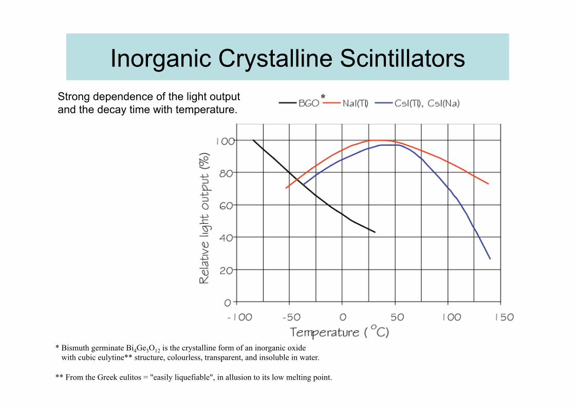
* Strong dependence of the light output and the decay time with temperature.
* Bismuth germinate Bi4Ge3O12 is the crystalline form of an inorganic oxide with cubic eulytine** structure, colourless, transparent, and insoluble in water. ** From the Greek eulitos = "easily liquefiable", in allusion to its low melting point.
Inorganic Crystalline Scintillators
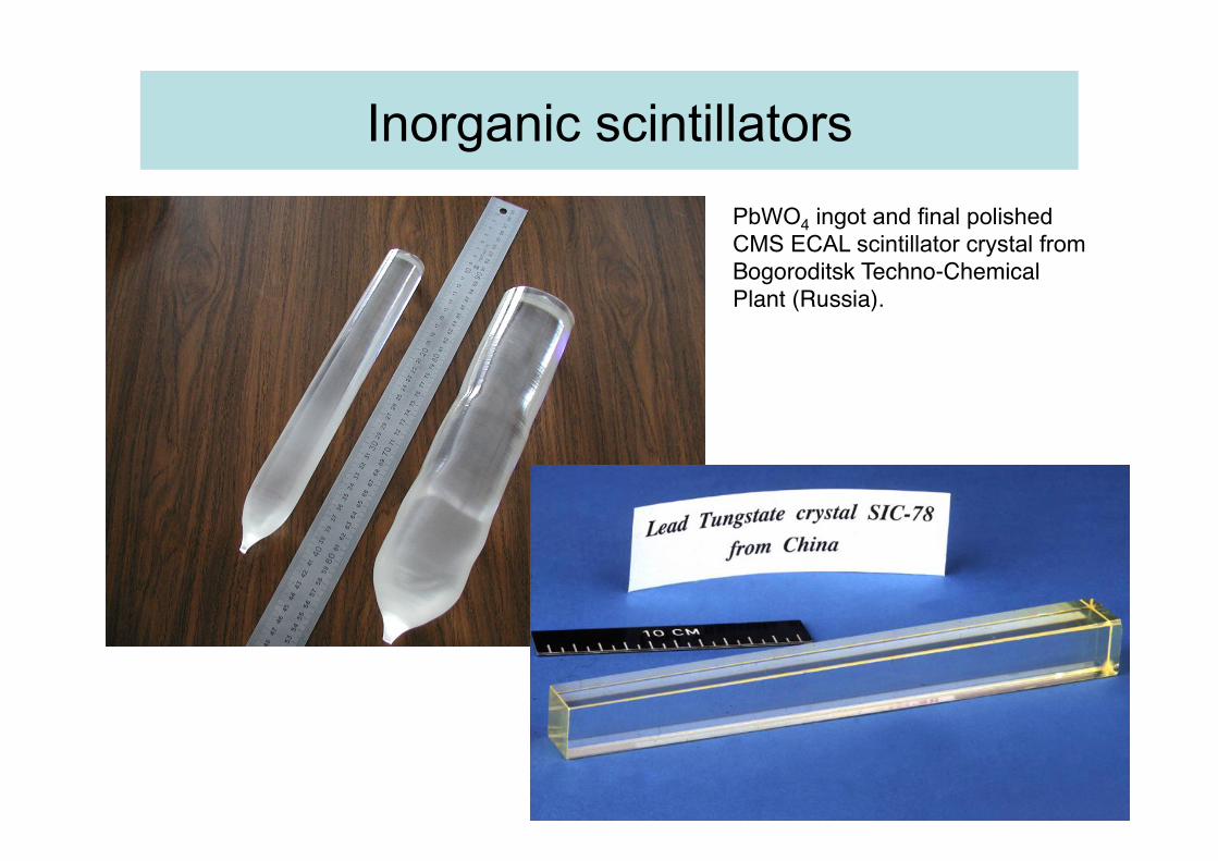
Inorganic scintillators PbWO4 ingot and final polished CMS ECAL scintillator crystal from Bogoroditsk Techno-Chemical Plant (Russia).

Also here one finds 2 time constants: from a few ns to 1 µs.
from C. D'Ambrosio, Academic Training, 2005
Liquified Noble Gases: LAr, LXe, LKr

Common materials Density (g/cm3)
λemiss (nm)
#photon/MeV τ(ns)
NaI(Tl) 3.7 410 40000 230 hygrosc.
CsI(Tl) 4.5 560 45000 1100 hygrosc.
BGO 7.1 480 8000 300
BaF2 4.9 220 / 310
2300/ 10000
0.8 / 630
CeF3 6.2 320 5500 27 rad. hard
plastic 1.03 430 10000 2…5 easy handling
= good = bad
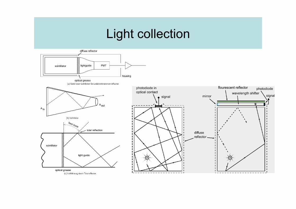
Light collection

Light collection

Optical fibers
corepolystyrene
n=1.59
cladding(PMMA)n=1.49
typically <1 mm
typ. 25 µmlight transport by total internal reflection
θ
n1
n2
°≈≥ 6.69arcsin1
2nn
θ %1.34
=Ωπd
in one direction
and absorption length: λ>10 m for visible light
corepolystyrene
n=1.59
cladding(PMMA)n=1.49
25 µm
fluorinated outer claddingn=1.42
25 µm%3.5
4=
Ωπd
multi-clad fibres for improved aperture
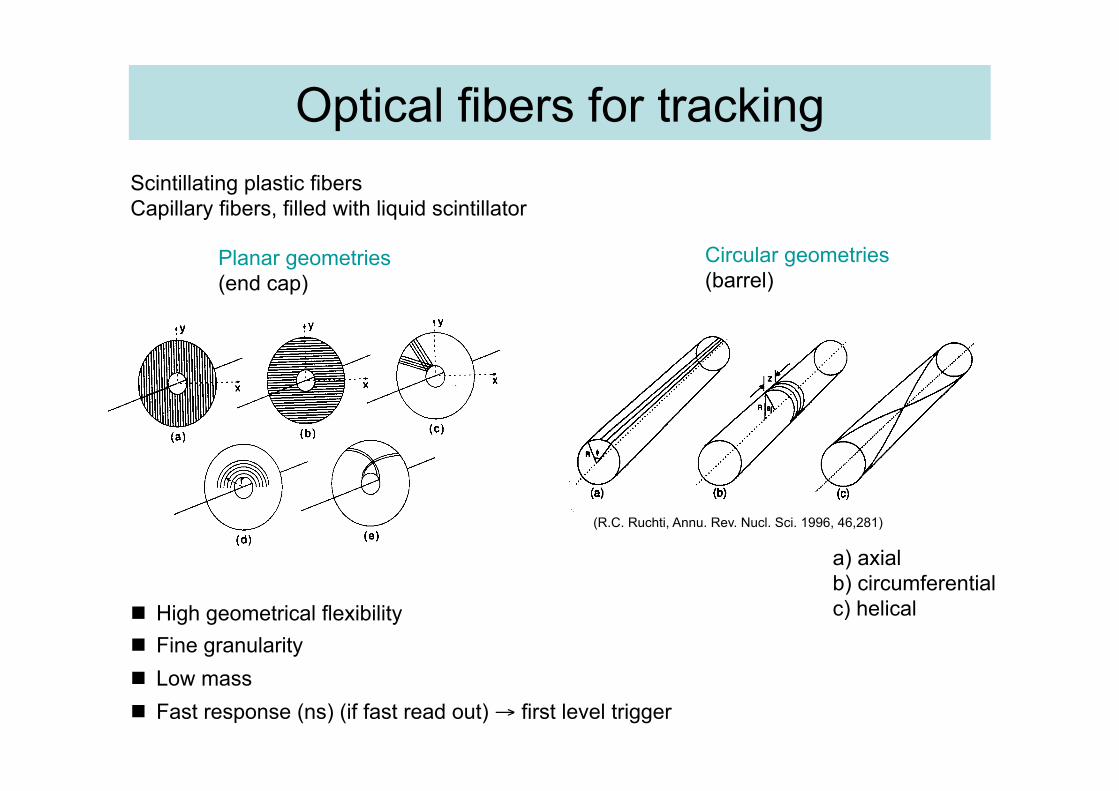
Optical fibers for tracking Scintillating plastic fibers Capillary fibers, filled with liquid scintillator
Planar geometries (end cap)
Circular geometries (barrel)
n High geometrical flexibility n Fine granularity n Low mass n Fast response (ns) (if fast read out) → first level trigger
(R.C. Ruchti, Annu. Rev. Nucl. Sci. 1996, 46,281)
a) axial b) circumferential c) helical

Scintillating fiber tracking
Charged particle passing through a stack of scintillating fibers (diam. 1mm)
(H. Leutz, NIM A 364 (1995) 422)
Hexagonal fibers with double cladding. Only central fiber illuminated. Low cross talk !
Photon Detectors • Purpose:
– Convert light into detectable (electronic) signal
• Principle: – Use photoelectric effect to convert photons (γ) to photoelectrons (pe)
• Standard requirements: – High sensitivity, usually expressed as:
• quantum efficiency:
• radiant sensitivity S(mA/W):
– Low intrinsic noise – Low gain fluctuations – High active area
γNN
QE pe=(%)
)()/(124(%)
nmWmASQE
λ⋅≈
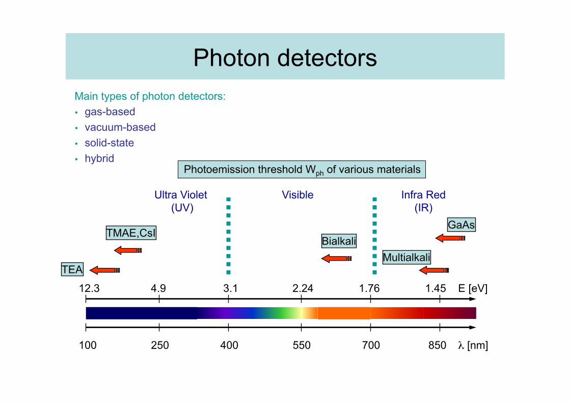
Main types of photon detectors: � gas-based � vacuum-based � solid-state � hybrid
Photon detectors
Photoemission threshold Wph of various materials
100 250 400 550 700 850 λ [nm]
12.3 4.9 3.1 2.24 1.76 1.45 E [eV]
Visible Ultra Violet (UV)
Multialkali Bialkali
GaAs
TEA
TMAE,CsI
Infra Red (IR)
Photon detectors
γ
γ
e-
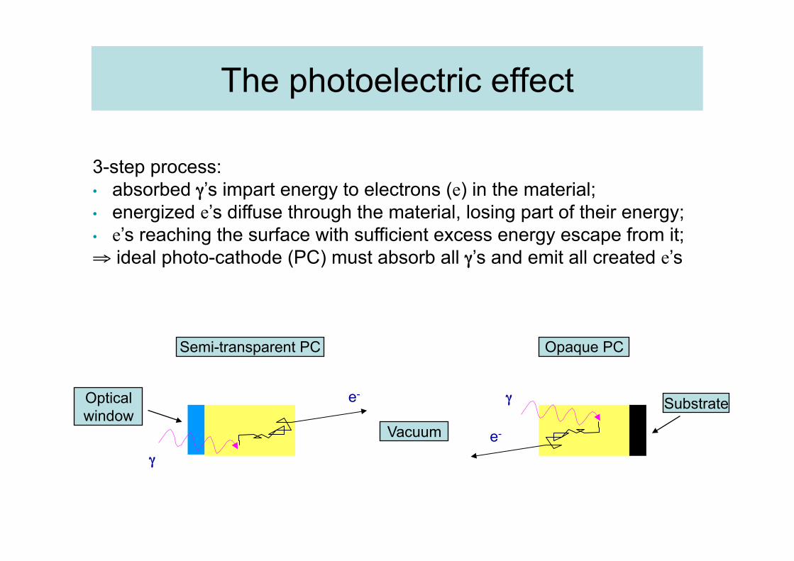
Optical window
Semi-transparent PC
Vacuum
Opaque PC
Substrate e-
3-step process: • absorbed γ’s impart energy to electrons (e) in the material; • energized e’s diffuse through the material, losing part of their energy; • e’s reaching the surface with sufficient excess energy escape from it; ⇒ ideal photo-cathode (PC) must absorb all γ’s and emit all created e’s
The photoelectric effect

Energy-band model in semi-conductor PC
AGph EEWhE +=>= νγ
Band gap EG
γ energy Eγ
h
e-
(Photonis) Electron affinity EA
Photoemission threshold Wph
Standard model NEA material
Gph EW =
Negative electron affinity EA

Bialkali: SbKCs, SbRbCs Multialkali: SbNa2KCs (alkali metals have low work function)
(Hamamatsu)
GaAsP GaAs
CsTe (solar blind)
Multialkali Bialkali
Ag-O-Cs
Photon energy Eγ (eV) 12.3 3.1 1.76 1.13
QE’s of typical photo-cathodes
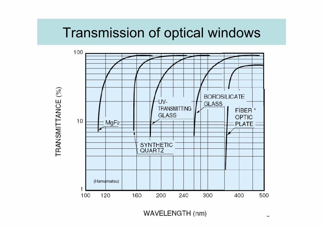
Transmission of optical windows

Scintillator-Photomultiplier system
(in-)organic material à scintillation light
photomultiplier à signal amplification
light guide à transmission scint. to tube

Photomultiplier tubes (PMTs)
• Basic principle: – Photo-emission from photo-
cathode – Secondary emission (SE)
from N Dynodes: • dynode gain g ≈ 3 – 50
(function of incoming electron energy E)
• total gain M:
• Example: – 10 dynodes with g = 4 – M = 410 ≈ 106
∏=
=N
iigM
1

Approximately the same as the Photo Electric Effect. On electron impact, energy is transferred directly to the electrons in the secondary electron emission material allowing a number of secondary electrons to escape. Since the conducting electrons in metals hinder this escape, insulators and semiconductors are used.
Materials in common use are: Ag/Mg, Cu/Be and Cs/Sb. Use has also been made of negative affinity materials as dynodes, in particular GaP.
Secondary Electron Emission
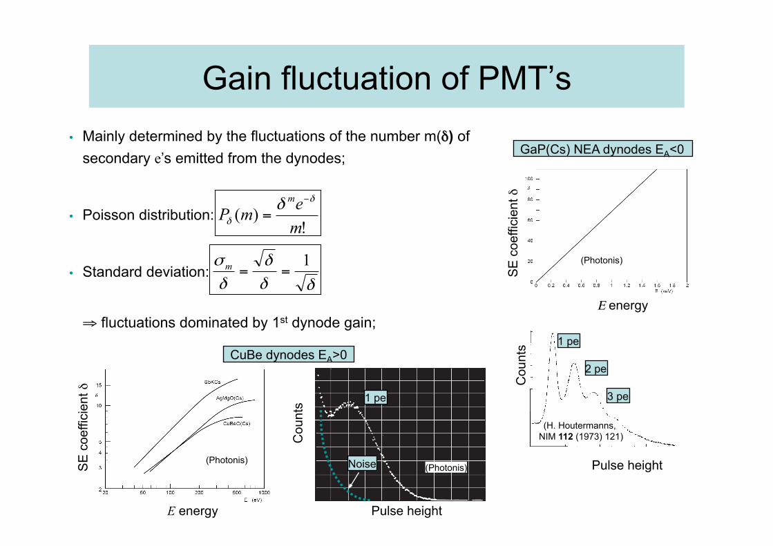
� Mainly determined by the fluctuations of the number m(δ) of secondary e’s emitted from the dynodes;
� Poisson distribution:
� Standard deviation:
⇒ fluctuations dominated by 1st dynode gain;
!)(
memP
m δ
δ
δ −
=
δδδ
δσ 1
==m
Pulse height
(H. Houtermanns, NIM 112 (1973) 121)
GaP(Cs) NEA dynodes EA<0
SE
coe
ffici
ent δ
Ε energy
(Photonis)
1 pe
2 pe
3 pe
Cou
nts
(Photonis)
1 pe
Noise
CuBe dynodes EA>0
Pulse height
Cou
nts
SE
coe
ffici
ent δ
E energy
(Photonis)
Gain fluctuation of PMT’s

Dynode configurations of PMT’s Traditional Position-sensitive
Mesh
Metall-channel (fine-machining techniques)
PMT’s are in general very sensitive to magnetic fields, even to earth field (30-60 µT). è Magnetic shielding required.
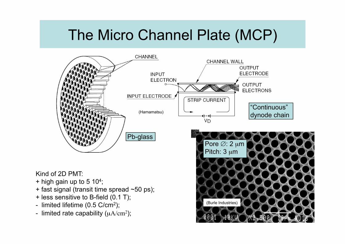
(Hamamatsu) “Continuous” dynode chain
Pb-glass
Kind of 2D PMT: + high gain up to 5 104; + fast signal (transit time spread ~50 ps); + less sensitive to B-field (0.1 T); - limited lifetime (0.5 C/cm2); - limited rate capability (µA/cm2);
(Burle Industries)
Pore ∅: 2 µm Pitch: 3 µm
The Micro Channel Plate (MCP)
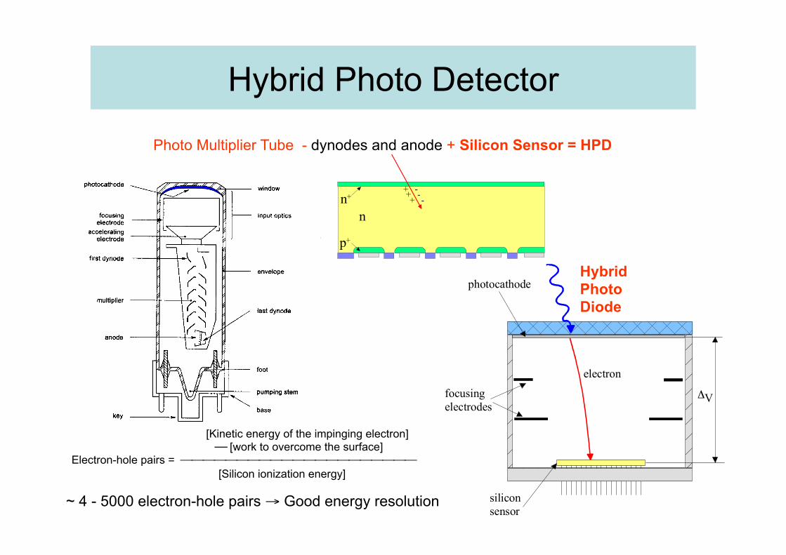
Photo Multiplier Tube - dynodes and anode + Silicon Sensor = HPD
Hybrid Photo Diode
p+
n+
n
+ -+ -+ -
ΔV
photocathode
focusing electrodes
siliconsensor
electron
~ 4 - 5000 electron-hole pairs → Good energy resolution
[Kinetic energy of the impinging electron] ⎯ [work to overcome the surface]
Electron-hole pairs = ⎯⎯⎯⎯⎯⎯⎯⎯⎯⎯⎯⎯⎯⎯⎯⎯⎯⎯⎯⎯⎯ [Silicon ionization energy]
Hybrid Photo Detector
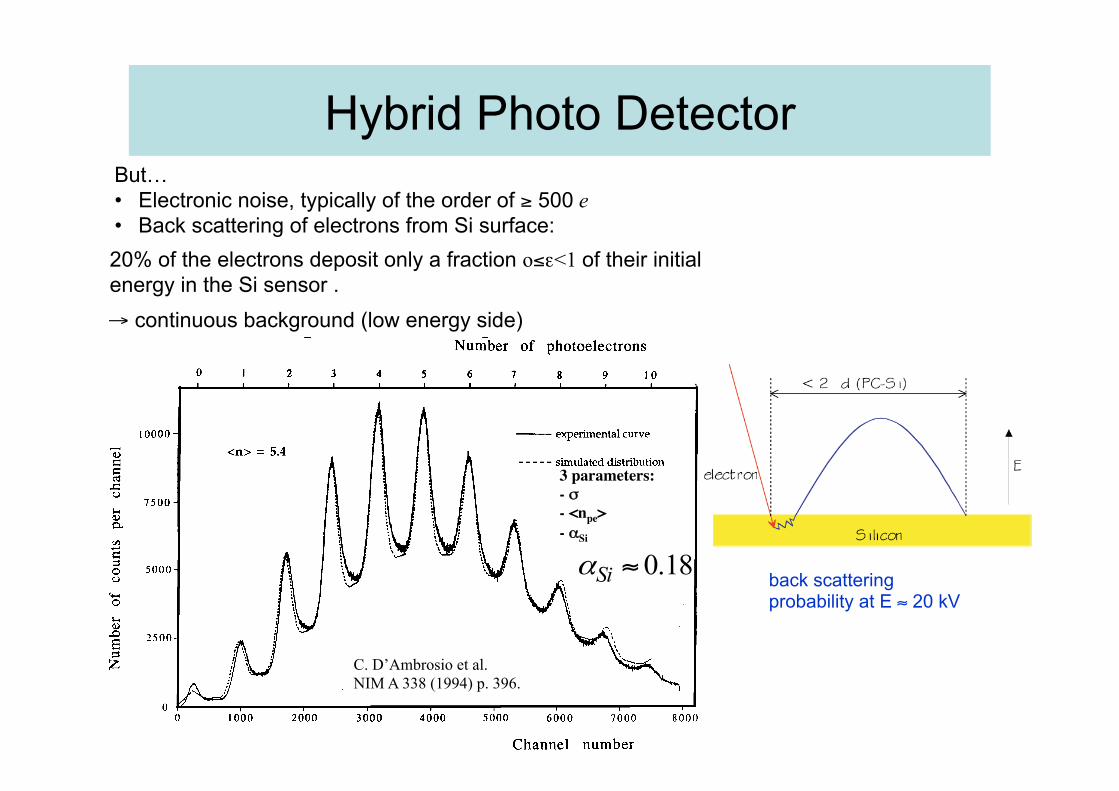
But… • Electronic noise, typically of the order of ≥ 500 e • Back scattering of electrons from Si surface:
18.0≈Siα back scattering probability at E ≈ 20 kV
20% of the electrons deposit only a fraction o≤ε<1 of their initial energy in the Si sensor . → continuous background (low energy side)
C. D’Ambrosio et al. NIM A 338 (1994) p. 396.
3 parameters: - σ - <npe> - αSi
Hybrid Photo Detector

Solid-state photon detectors
• Photodiodes: – P(I)N type – p layer very thin (< 1 µm), as
visible light is rapidly absorbed by silicon
– High QE(80% at 700 nm) – No gain: cannot be used for single
photon detection
• Avalanche phtodiode: – High reverse bias voltage: typ.
100-200 V – due to doping profile, high internal
field and avalanche multiplication – High gain: typ. 100-1000
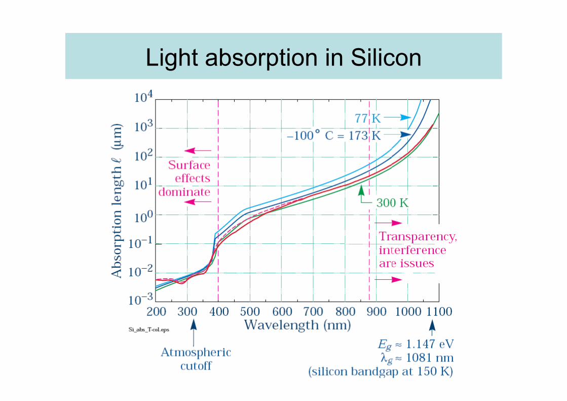
Light absorption in Silicon
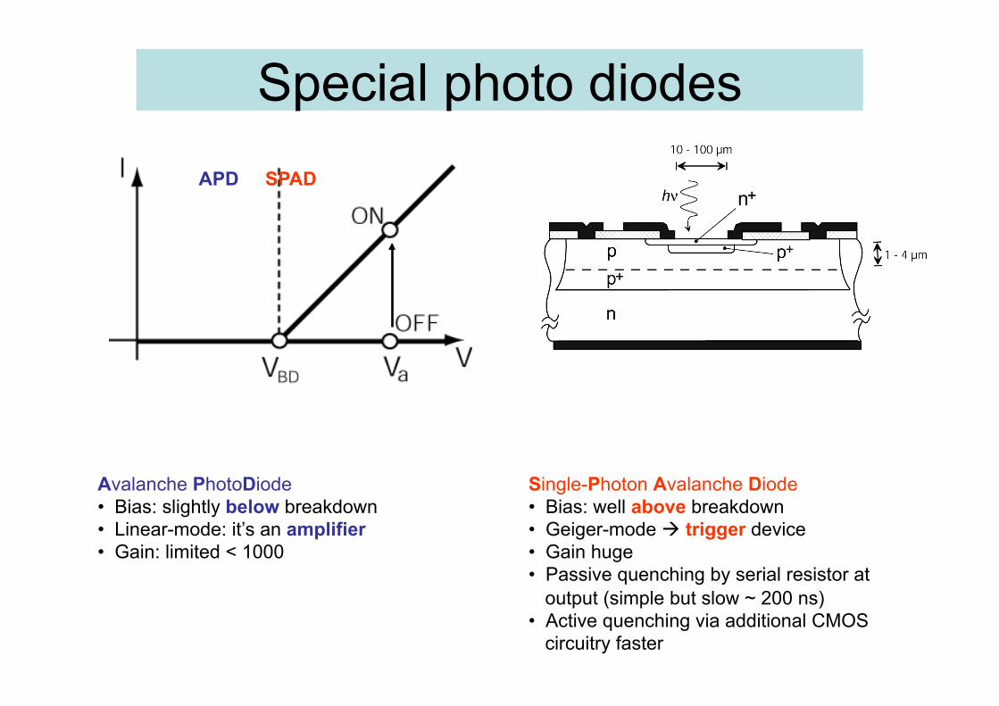
APD SPAD
Special photo diodes
Avalanche PhotoDiode • Bias: slightly below breakdown • Linear-mode: it’s an amplifier • Gain: limited < 1000
Single-Photon Avalanche Diode • Bias: well above breakdown • Geiger-mode à trigger device • Gain huge • Passive quenching by serial resistor at
output (simple but slow ~ 200 ns) • Active quenching via additional CMOS
circuitry faster
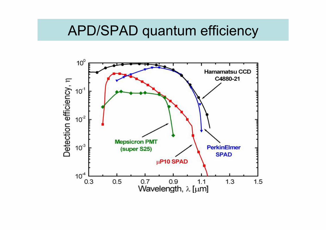
APD/SPAD quantum efficiency
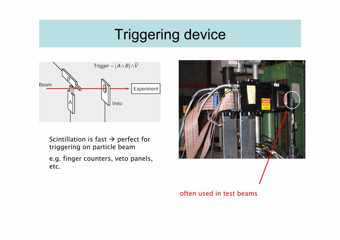
Triggering device
Scintillation is fast à perfect for triggering on particle beam e.g. finger counters, veto panels, etc.
often used in test beams