lecture (6) interface electronic circuits
TRANSCRIPT

AMSS-MSc Prof. Kasim Al-Aubidy 1
Lecture (6)
Interface Electronic Circuits Part: 2
Prof. Kasim M. Al-Aubidy
Philadelphia University-Jordan

AMSS-MSc Prof. Kasim Al-Aubidy 2
Bridge Circuits:
The Wheatstone bridge circuits are popular and very effective implementations of
the ratiometric technique on a sensor level.
Impedances Z may be either active or reactive, that is they may be either simple
resistances, like in the piezoresistive gauges, or capacitors, or inductors, or
combinations of the above.
For a pure resistor, the impedance is R, for an ideal capacitor, the magnitude of its
impedance is equal to 1/(2pfC) and for an inductor, it is 2pfL, where f is the frequency
of the current passing through the element. The bridge output voltage is represented by:
The bridge is considered to be in a balanced state when the
following condition is met:

AMSS-MSc Prof. Kasim Al-Aubidy 3
Under the balanced condition, the output voltage is zero.
When at least one impedance in the bridge changes, the bridge becomes
imbalanced and the output voltage goes either in a +ve or -ve direction.
To determine the bridge sensitivity with respect to each impedance;
By summing these equations, we obtain the bridge sensitivity:
Only the adjacent pairs of the impedances {i.e., (Z1 & Z2), (Z3 & Z4)} have to be identical in
order to achieve the ratiometric compensation (such as the temperature stability, drift, etc.).
It should be noted that impedances in the balanced bridge do not have to be equal, as long as
a balance of the ratio is satisfied. In many practical circuits, only one impedance is used as a
sensor, thus for Z1 as a sensor, the bridge sensitivity becomes;

AMSS-MSc Prof. Kasim Al-Aubidy 4
Disbalanced Bridge: (Wheatstone bridge circuit) (Deflection Method of Measurement)
It is based on a detecting the voltage across the bridge
diagonal. The bridge output voltage is a nonlinear function of
a disbalance (), where the sensor’s resistance Rv = R(1+ ).
For a small change ( < 0.05), the bridge output may be
considered quasi-linear.
The bridge maximum sensitivity (α) is obtained when R1= R2
and R3 = R.
When R1 >> R2 or R2 >> R1, the bridge output voltage is
decreased.
The bridge sensitivity may be expressed as:
where; k = R1/R2
If the bridge is fed by a current source (i), rather by a voltage
source, its output voltage for small and a single variable
component is represented by;
AMSS-MSc Prof. Kasim Al-Aubidy 5
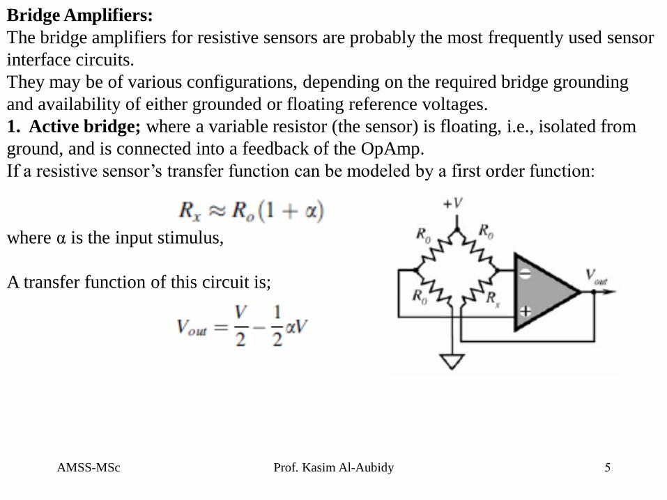
Bridge Amplifiers:
The bridge amplifiers for resistive sensors are probably the most frequently used sensor
interface circuits.
They may be of various configurations, depending on the required bridge grounding
and availability of either grounded or floating reference voltages.
1. Active bridge; where a variable resistor (the sensor) is floating, i.e., isolated from
ground, and is connected into a feedback of the OpAmp.
If a resistive sensor’s transfer function can be modeled by a first order function:
where α is the input stimulus,
A transfer function of this circuit is;

AMSS-MSc Prof. Kasim Al-Aubidy 6
Bridge Amplifiers:
2. A circuit with a floating bridge and floating reference
voltage source (V), may provide gain which is determined
by a feedback resistor whose value is nRo:
3. A bridge with the asymmetrical resistors (R6=Ro):
It requires a floating reference voltage source V:
AMSS-MSc Prof. Kasim Al-Aubidy 7
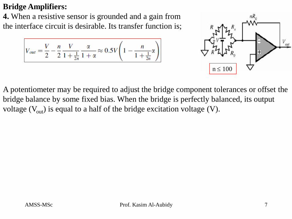
Bridge Amplifiers:
4. When a resistive sensor is grounded and a gain from
the interface circuit is desirable. Its transfer function is;
A potentiometer may be required to adjust the bridge component tolerances or offset the
bridge balance by some fixed bias. When the bridge is perfectly balanced, its output
voltage (Vout) is equal to a half of the bridge excitation voltage (V).
n 100

AMSS-MSc Prof. Kasim Al-Aubidy 8
Data Transmission:
Signal from a sensor may be transmitted to a receiving end of the system either in a
digital format or analog. Transmission in a digital format has several advantages.
The sensor’s output signal is transmitted to the receiving site in an analog form.
Depending on connection, the transmission methods can be divided into a 2, 4, and 6-
wire methods.
1. Two-wire Transmission:
Two-wire analog transmitters are used to couple sensors to other devices.
Two wires can be used to transmit either voltage or current (industry standard). The
current varies in the range (4 to 20) mA, which represents the entire span of the
measured variable.
An advantage of the two wire
method is that the transmitting
current is independent of the
connecting wires resistance (as
long as they do not change) and
thus of the transmission line
length (within the limits).

AMSS-MSc Prof. Kasim Al-Aubidy 9
Four-wire transmission:
When a sensor has a relatively low resistance (order of 100 Ω), such as RTDs or
piezoresistors, the connecting wire resistances pose a serious problem since they
alter the excitation voltage across the sensor. This problem can be solved by using
4-wire method.
A sensor is connected to the interface circuit through four wires. Two wires are
connected to a current source and two others to a voltmeter or amplifier.
A voltage drop across the resistor (Rx) is;
which is independent of any resistances
(r) of the connecting wires.
The 4-wire method is a very powerful
means of measuring resistances of
remote detectors and is used in industry
and science.

AMSS-MSc Prof. Kasim Al-Aubidy 10
3. Six-Wire Sensing:
When a Wheatstone bridge circuit is remotely located, voltage across the bridge plays
an important role in the bridge temperature stability.
Long transmitting wires may introduce unacceptably high resistance in series with the
bridge excitation voltage, which interferes with the temperature compensation. This
problem may be solved by providing two additional wires to feed the bridge with
voltage and to dedicate two wires to measuring the voltage across the bridge.
Note: The actual excitation voltage across
the bridge and the bridge differential output
voltage are measured by a high-input
impedance voltmeter with negligibly small
input currents. Thus, the accurate bridge
voltages are available at the data
processing site without being affected by
long transmission lines.
AMSS-MSc Prof. Kasim Al-Aubidy 11
Noise in Sensors and Circuits:
There are two basic classifications of noise;
1. Inherent noise; which is noise arising within the circuit, and
2. Interference (transmitted) noise; which is noise picked up from outside the circuit.
1. Inherent Noise:
A signal, which is amplified and converted from a sensor into a digital form, should
be regarded not just by its magnitude and spectral characteristics, but also in terms
of a digital resolution.
Noise can be produced by the monolithic amplifiers and other components, which
are required for the feedback, biasing, bandwidth limiting, etc.
The noise signals (voltage and current) result from physical mechanisms within the
resistors and semiconductors that are used to fabricate the circuits.
There are several sources of noise whose combined effect is represented by the
noise voltage and current generators.
One cause for noise is a discrete nature of electric current because current flow is
made up of moving charges, and each charge carrier transports a definite value of
charge

AMSS-MSc Prof. Kasim Al-Aubidy 12
In a resistor, these thermal motions cause Johnson noise to result. The mean-square
value of noise voltage (which is representative of noise power) can be calculated
from;
where; k = 1.38*10-23 J/K (Boltzmann constant), T is temperature in K, R is the resistance in
Ω, and f is the bandwidth over which the measurement is made.
Even a simple resistor is a source of noise, a small resistors generate extremely
small noise.
Noise voltage is proportional to square root of the bandwidth. It implies that if we
reduce the bandwidth 100 times, noise voltage will be reduced by a factor of 10.
Another type of noise results because of dc current flow in semiconductors. It is
called shot noise, which is also white noise. Its value becomes higher with the
increase in the bias current. This is the reason why in FET and CMOS
semiconductors the current noise is quite small. A convenient equation for shot
noise is;
where I is a semiconductor junction current in pA and f is a bandwidth of interest in Hz.

AMSS-MSc Prof. Kasim Al-Aubidy 13
Pink noise:
An additional ac noise mechanism exists at
low frequencies.
Both the noise voltage and noise current
sources have a spectral density roughly
proportional to 1/f, which is called the pink
noise, because of the higher noise contents
at lower frequencies.
This 1/f noise occurs in all conductive materials, therefore it is also associated with
resistors.
At extremely low frequencies it is impossible to separate the 1/f noise from dc drift
effects. The 1/f noise is sometimes called a flicker noise.
A combined noise from all voltage and current sources is given by sum of squares
of individual noise voltages:
where T is time of observation, e is noise voltage and t is time.

AMSS-MSc Prof. Kasim Al-Aubidy 14
2. Interference (Transmitted) noise:
Noise comes from a source which often cannot be identified. Examples of the
sources are: voltage surges in power lines, lightnings, sun activity, change in
ambient temperature, etc.
These interferences propagate toward the sensor and the interface circuit, and to
present a problem eventually must appear at the output.
They somehow must affect the sensing element inside the sensor, its output
terminals or the electronic components in the circuit. Both the sensor and circuit act
as receivers of the interferences.

AMSS-MSc Prof. Kasim Al-Aubidy 15
There can be several classifications of transmitted noise, depending on how it
affects the output signal, how it enters the sensor or circuit, etc.
With respect to its relation to the output signals, noise can be either additive or
multiplicative.
Additive noise (en) is added to the useful signal (Vs) and
mixed with it as a fully independent voltage (or current);
Note: the noise magnitude does not change when the actual
signal changes. As long as the sensor and interface electronics
can be considered linear, the additive noise magnitude is totally
independent of the signal magnitude
Multiplicative noise affects the sensor’s transfer function
or the circuit’s nonlinear components in such a manner as
Vs signal’s value becomes altered or modulated by the
noise:
where N(t) is a function of noise.

AMSS-MSc Prof. Kasim Al-Aubidy 16
Differential Technique Method:
To improve noise stability against transmitted
additive noise, sensors are combined in pairs,
they are fabricated in a dual form whose output
signals are subtracted from one another.
Since additive noise is specific for the linear or quasilinear sensors and circuits, the
reference sensor does not have to be subjected to any particular stimulus.
Both sensors are subjected to identical transmitted noise (noise generated inside the
sensor cannot be cancelled by a differential technique), it is a common-mode noise.
This means that noisy effects at both sensors are in-phase and have the same
magnitude. If both sensors are identically influenced by common mode spurious
stimuli, the subtraction removes the noise component.
The quality of noise rejection is described by a number which is called the
common-mode rejection ratio (CMRR):
The ratio shows how many times stronger the actual stimulus will be represented at
the output, with respect to a common mode noise having the same magnitude.

AMSS-MSc Prof. Kasim Al-Aubidy 17
Electric Shielding:
Interferences to electric fields can be significantly reduced by appropriate shielding of
the sensor and circuit, especially of high impedance and nonlinear components.
Each shielding problem must be analyzed separately and carefully.
It is very important to identify the noise source and how it is coupled to the circuit.
A shielding serves two purposes; 1. It confines noise to a small region, to prevent noise from getting into nearby circuits.
2. If noise is present in the circuit, shields can be placed around critical parts to prevent the
noise from getting into sensitive portions of the detectors and circuits. These shields may
consist of metal boxes around circuit regions or cables with shields around the center
conductors.
A noise current is defined as;
and actually produces noise voltage;
For example: if Cs=2.5pf, Z=10 kΩ (resistor) and
en= 100 mV, at 1.3 MHz. Then, the output noise
will be 20 mV.
AMSS-MSc Prof. Kasim Al-Aubidy 18
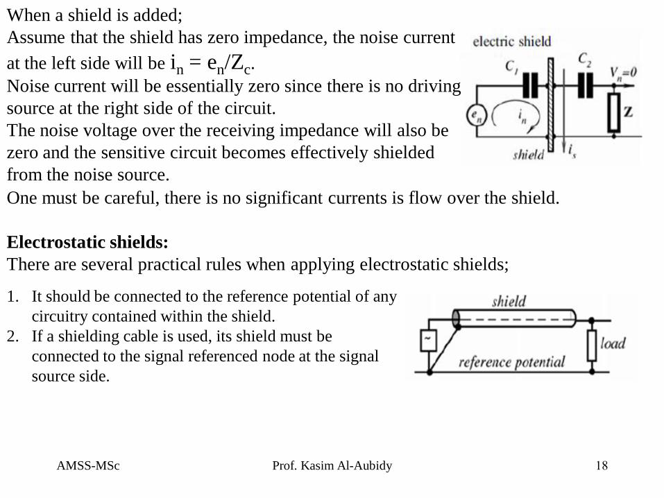
When a shield is added;
Assume that the shield has zero impedance, the noise current
at the left side will be in = en/Zc.
Noise current will be essentially zero since there is no driving
source at the right side of the circuit.
The noise voltage over the receiving impedance will also be
zero and the sensitive circuit becomes effectively shielded
from the noise source.
One must be careful, there is no significant currents is flow over the shield.
Electrostatic shields:
There are several practical rules when applying electrostatic shields;
1. It should be connected to the reference potential of any
circuitry contained within the shield.
2. If a shielding cable is used, its shield must be
connected to the signal referenced node at the signal
source side.

AMSS-MSc Prof. Kasim Al-Aubidy 19
3 If the shield is split into sections, as might occur
if connectors are used, the shield for each
segment must be tied to those for the adjoining
segments, and ultimately connected only to the
signal referenced node.
4. The number of separate shields required in a
data acquisition system is equal to the number of
independent signals that are being measured.
5. If a sensor is enclosed into a shield box and data
are transmitted via a shielded cable. The cable
shield must be connected to the box.
6. Never allow the shield to be at any potential with
respect to the reference potential.
7 Connect shields to a ground via short wires to minimize inductance. This is especially
important when both analog and digital signals are transmitted.

AMSS-MSc Prof. Kasim Al-Aubidy 20
Magnetic Shielding:
Proper shielding may reduce noise resulting from electrostatic and electrical fields.
It is much more difficult to shield against magnetic fields because it penetrates
conducting materials.
Since magnetic shielding is very difficult, the most effective approach at low
frequencies is to;
minimize the strength of magnetic fields,
Minimize the magnetic loop area at the receiving end, and
selecting the optimal geometry of conductors.
A typical shield placed around a
conductor and grounded at one end
has little if any effect on the
magnetically induced voltage in
that conductor.
Reduction of a transmitted
magnetic noise by powering a load
device through a coaxial cable.

AMSS-MSc Prof. Kasim Al-Aubidy 21
Ground Loops and Ground Isolation:
A power supply bus carries supply currents to
all stages.
A ground bus also carries supply currents, but,
in addition, it is often used to establish a
reference base for an electrical signal. For any
measurement circuit cleanliness of a reference
base is essential.
Interaction of the two functions (power supply
and reference) may lead to a problem which is
known as ground loop.

AMSS-MSc Prof. Kasim Al-Aubidy 22
Seebeck Noise:
This noise is a result of the Seebeck effect, which is manifested as the generation of
an electromotive force (e.m.f.) when two dissimilar metals are joined together.
The Seebeck e.m.f. is small and for many sensors may be simply ignored.
When absolute accuracy on the order of 10–100 mV is required, that noise must be
taken into account.
Seebeck e.m.f. may be eliminated by a proper circuit layout and thermal balancing.
It is a good practice to limit the number of junctions between the sensor and the
front stage of the interface circuit. Avoid connectors, sockets, switches and other
potential sources of e.m.f. to the extent possible.

AMSS-MSc Prof. Kasim Al-Aubidy 23
References:
1. Jacob Fraden, “Handbook of Modern Sensors; Physics, Design, and Applications”, Fourth Edition,
Springer Press 2010.
2. Kelley CT (2003) Solving nonlinear equations with Newton’s method, No. 1 Fundamentals of
Algorithms. SIAM, Philadelphia, PA
3. ISO guide to the expression of uncertainty in measurements (1993) International Organization for
Standardization, Geneva, Switzerland
4. Taylor BN, Kuyatt CE (1994) Guidelines for evaluation and expressing the uncertainty of NIST
measurement results. NIST Technical Note 1297. US Government Printing Office, Washington DC
5. Widlar RJ (1980) Working with high impedance Op Amps, AN24, Linear Application Handbook.
National Semiconductor
6. Sheingold DH (ed) (1986) Analog-Digital Conversion Handbook. 3rd ed., Prentice-Hall, Englewood
Cliffs, NJ.
7. Williams J (1990) Some techniques for direct digitization of transducer outputs, AN7, Linear Technology
Application Handbook.
8. Coats MR (1991) New technology two-wire transmitters. Sensors 8(1)