lecture 6: deprocessing - security groupsecurity.cs.rpi.edu/.../lecture6_deprocessing.pdf ·...
TRANSCRIPT

CSCI 4974 / 6974Hardware Reverse Engineering
Lecture 6: Deprocessing

What is deprocessing?
● Reversing the manufacturing process to reveal features made early on
● Based on, but not identical to, fab processing● Inherently destructive to sample

Types of deprocessing
● Material removal– Selective
– Non-selective
● Staining

Wet etching
● Submerge sample in tank of corrosive liquid● Make sure all etchant is gone after!
– Etchant residue on surface can cause further damage to sample after removal from tank
● Generally isotropic● Sonication/stirring may help uniformity● Lots of processes: http://siliconpr0n.org/wiki/doku.php?id=delayer:wet

Wet etching
● Surface must be extremely clean beforehand– Dirt/package residue on surface will mask etch

HF wet etch
● Target: SiO2
– SiO2 + 4HF => SiF
4 (g) + 2H
2O
– SiO2 + 6HF => H
2SiF
6 (aq) + 2 H
2O
– Will also damage Al, but not poly or Cu
● Will undercut wires if overetched● Poor choice for deep etches (hard to control)

HF toxicity
● Handle with extreme care!● Emits toxic vapors● Weakly acidic (does not cause immediate pain)● Fluorine toxicity is the real problem
– Removes Ca+ from cells, eats bones
– Clogs things with insoluble CaF

HF wet etch
● Removal of oxide– Exposing poly on 1-metal chips
– Stripping dies to active layer
– Removing ILD after CMP so wires stick up
● Ingredient in Dash etch (covered later today)

HF wet etch
● Use a pH buffer (BOE) to improve evenness– Also reduces damage to metal
● Do not use glass labware!● Use dedicated plastic labware
– Keep free of metal ions (will leave residue)
– Keep free of oxidizers (will damage Si)
● Stirring OK, do not use ultrasound– Will rip wires and oxide chunks off

Stress induced ILD cracking
● Not sure of cause, could be many things● Overheating during decap● Etching too fast● Mechanical shock

Metal fluoride crystals
● Caused by HF eating metal● Difficult to remove● Workarounds
– Use BOE to reduce metal damage
– Remove metal before etching with HF

Wet etching for metal
● Aluminum– 65% phosphoric acid @ 50C
● Copper
– 6 parts 3% H2O
2 + 1 part concentrated HCl
● Tungsten– HCl
● Tables of etch rates and mixtures published in fab journals / textbooks

Wet etching for silicon nitride
● Phosphoric acid– 10:1 selectivity vs oxide
– 4x faster than HF on nitride
– But eats most metals
– May be useful for thinning overglass
● HF– Doesn't attack metal as fast
– Will attack ILD
Wet etching for barriers
● TiN [Beck's Failure Analysis]
– 9 parts 30% H2O
2
– 2 parts 35% NH4OH
– Etch ~3 min at 50-55C
– Can self-heat, may need water bath

CMP for deprocessing
● Gives very good results for planarized devices● Requires extremely level mounting of sample
– Can use adjustable jigs to correct for tilt

Lapping fixtures
● Center slides in and out for adjusting depth● Tripod jigs have adjustable tilt
– More expensive, but can get flatter results
● Conditioning pads around rim– Fluffs up pad
– Evens out slurry layer

Sample mounting
● Mount die in lapping jig with wax● Place sacrificial dies around sample
– Thickness matching is critical
● Die surface must be clean– Particles scratch!
● Do not mount dieat center (rings)

Edge rounding
● Sacrificial dies help correct with this● Boundary condition caused by pad elasticity

Tilted sample

Hand polishing
● Slide polishing fixture by hand over fixed pad● A bit cheaper● Takes a long time, not recommended

Machine polishing
● Polishing pad is mounted onspinning surface
● Drip abrasive suspention on pad● Press mounted sample against
spinning pad and move around● Moving jig helps uniformity
– Do not rotate about sample!

Machine polishing with finger
● Doesn't require a jig● Press die against spinning pad with finger● Dangerous to both operator and sample
– Not recommended!

Slurry pumping
● Slurry is corrosive and abrasive● How do you pump it?● Peristalstic pump!

Other notes
● Keep pads clean, do not allow abrasive slurry to dry up on pad
– Colloidal silica likes to clump and crystallize
● Maintain uniform, low flow rate on slurry drops– See http://siliconpr0n.org/wiki/doku.php?id=delayer:lapping

RIE for delayering
● Same RIE systems used for fab can be used for deprocessing!
● Selectivity may not be as good, but less chance of undercutting
● Requires more expensive infrastructure and plumbing for toxic gases

RIE for delayering
● Copper– Impossible, no useful gaseous compounds
● Aluminum– Cl or Cl-based gases
– Very selective against Si/SiO2
RIE for delayering
● SiO2
– CF4
– Also attacks Si :(

Dash etch
● Used to reveal doping– Figuring out tricky gates with weird sizing
– Reading implant-based ROMs
● Pre-requisite: Strip off metal, poly, and oxide– Etching too long may damage ROMs
– ROMs are weak implants and very sensitive!

Dash etch
● 3 parts 65% HNO3 (oxidizer)
● 1 part 48% HF (oxide etch)● 10-12 parts glacial acetic acid (diluent)

John McMaster variant
● Adjusted from original to use dilute HF– May be easier to get hold of
– Less HF fumes during mixing
– Slightly safer to handle, but still toxic/corrosive
● 3 parts 65% HNO3
● 4 parts 12% HF● 8 parts acetic acid
Dash etch
● Based on a common isotropic silicon etch
– 2HNO3 => NO
2 + NO + H2O + 2O [1]
– Si + 2O => SiO2
– HF then etches SiO2
– Acetic acid is just there to dilute and slow the reaction to a manageable rate
[1] http://cecs.anu.edu.au/files/posters09/44885380000000101.pdf

Dash etch
● Oxidation rate is weakly dopant-dependent● Set up an equilibrium, dopants tip it
– Undoped Si: Etch rate ≈ oxidation rate
– N-type: Etching dominates
– P-type: Oxidation dominates
● End result: P-type areas grow oxide● Typical process times: 5-15 sec
– May need to dilute / etch less for deep sub-μm– http://siliconpr0n.org/wiki/doku.php?id=delayer:dash

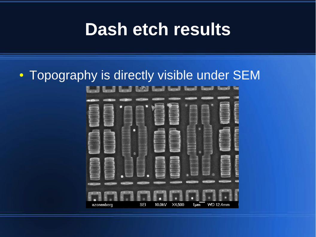
Dash etch results
● Oxide causes thin film interference colors
Dash etch results
● Topography is directly visible under SEM

Dash etch results

Dash etch results
● Use short stain times for deep submicron– Faint coloration starts at ~75 nm oxide
– May be too much for < 250 nm nodes!
● Example of slight over-stain on 180 nm

Dash etch
● Example of unusual doping (XC2C32A ZIA)● NMOS at left is larger than PMOS!

Questions?
● TA: Andrew Zonenberg <[email protected]>
● Image credit: Some images CC-BY from:
– John McMaster <[email protected]>● See also: “Etch rates for micromachining processing, pt 2”