lecture 4.2 and lecture 6 : introduction to electronics
TRANSCRIPT

EE110300 Practice of Electrical and Computer Engineering
Lecture 4.2 and Lecture 6 : Introduction to Electronics
For undergraduate students ofthe college of EECS, NTHU電機工程系 張慶元 教授
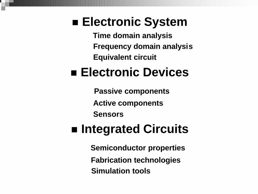
n Electronic SystemTime domain analysisFrequency domain analysisEquivalent circuit
n Electronic DevicesPassive components
Active componentsSensors
n Integrated CircuitsSemiconductor properties
Fabrication technologiesSimulation tools
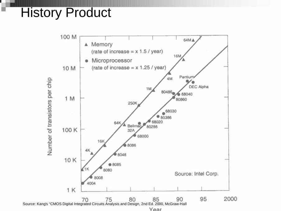
History Product
Source: Kang’s “CMOS Digital Integrated Circuits Analysis and Design, 2nd Ed. 2000, McGraw-Hall
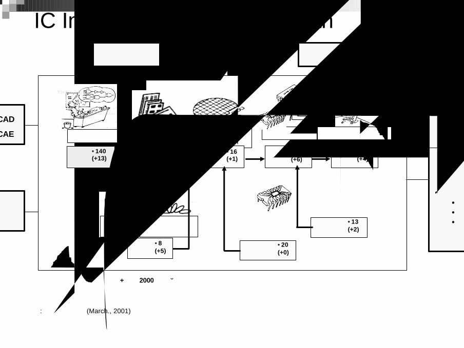
IC Industry Structure in Taiwan
資料來源 : 工研院電子所 (March., 2001)
晶粒測試及切割
長 晶 晶圓切割
設計
導線架
測試封裝製造光罩
晶圓
光罩設計電路設計 封 裝
化學品
CAD
CAE
材料
設備儀器 資金人力資源
服務支援
貨運
海關
科學園區•••
附註:數字表示公司家數,+表示2000年增加廠商家數
•140 (+13)
•4(-1)
•16 (+1)
•48(+6)
•37 (+4)
•8(+5)
•13(+2)
•20(+0)
成品測試
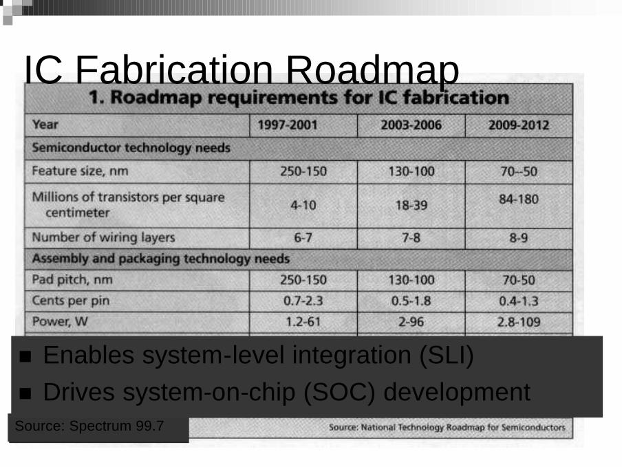
Source: Spectrum 99.7
n Enables system-level integration (SLI)n Drives system-on-chip (SOC) development
IC Fabrication Roadmap
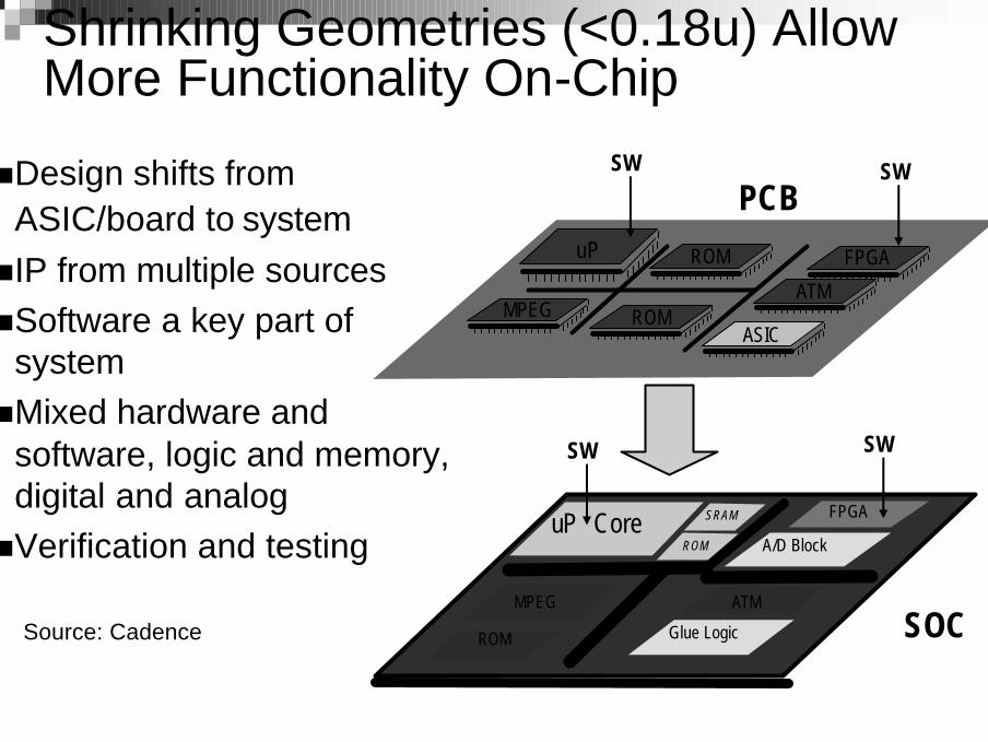
Shrinking Geometries (<0.18u) AllowMore Functionality On-Chip
uP FPGA
MPEGASIC
ATM
ROM
ROM
SW SW
SWSW
PCB
SOC
nDesign shifts from ASIC/board to systemnIP from multiple sourcesnSoftware a key part of
system nMixed hardware and
software, logic and memory, digital and analognVerification and testing
uP Core SRAM
ROM
ATMMPEG
ROM
FPGA
Glue Logic
A/D Block
Source: Cadence
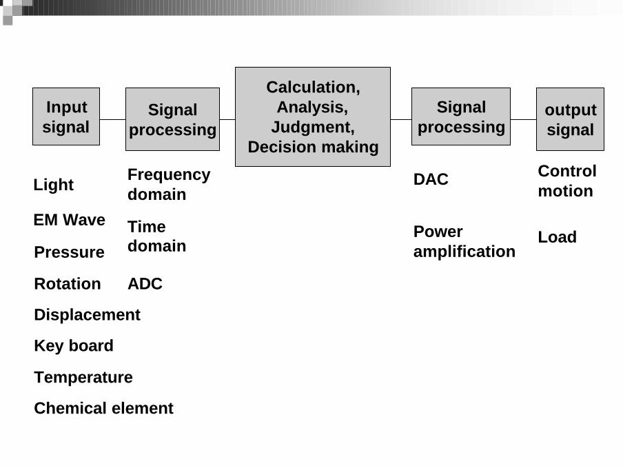
Inputsignal
Signalprocessing
Calculation,Analysis,
Judgment,Decision making
Signalprocessing
outputsignal
EM Wave
Light
Pressure
Chemical element
Displacement
Key board
Frequency domain
Time domain
ADCRotation
Temperature
DAC
Power amplification
Load
Control motion
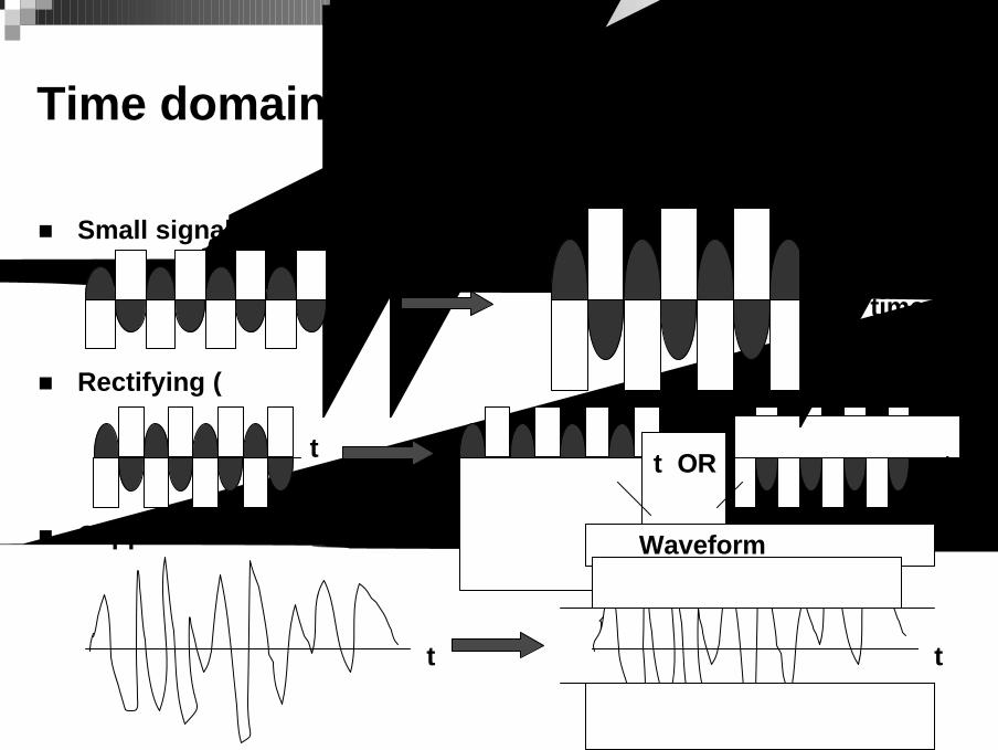
Time domain processing
n Small signal amplification ( 放大 )
n Rectifying ( 整流)
n Clipper/Limiter (截波/ 限波)
t OR
Waveform (波形)
time
t
t
t
t
t
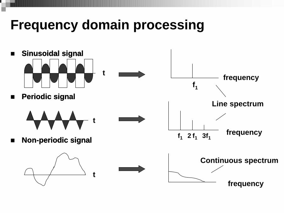
Frequency domain processing
n Sinusoidal signal
n Periodic signal
n Non-periodic signal
frequencyf1
n Sinusoidal signal
n Periodic signal
n Non-periodic signal
n Sinusoidal signal
n Periodic signal
n Non-periodic signalfrequencyf1 2 f1 3f1
Line spectrum
frequency
Continuous spectrum
(頻譜)
t
t
t
Frequency domain processing
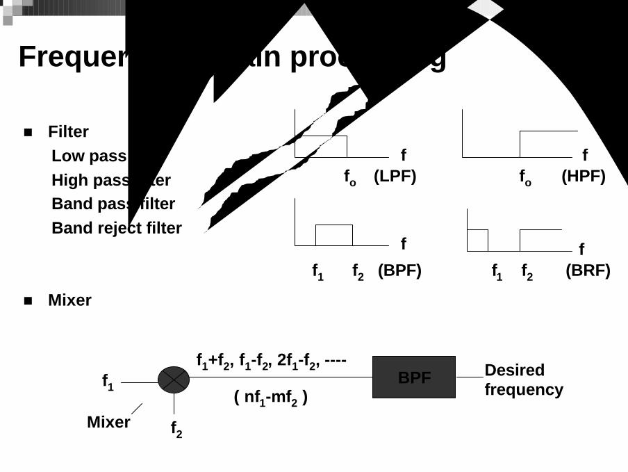
n Filter (濾波器)Low pass filter (低通)High pass filter (高通)Band pass filter (帶通)Band reject filter (帶拒)
n Mixer (混波器)
fo (LPF) fo (HPF)
f1 f2 (BPF) f1 f2 (BRF)
f f
f f
f1
f2
f1+f2, f1-f2, 2f1-f2, ----
( nf1-mf2 )BPF Desired
frequency
Mixer
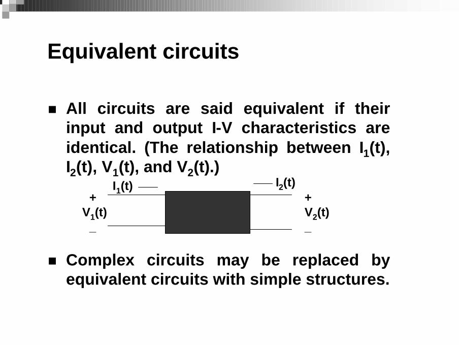
Equivalent circuits
n All circuits are said equivalent if their input and output I-V characteristics are identical. (The relationship between I1(t), I2(t), V1(t), and V2(t).)
n Complex circuits may be replaced by equivalent circuits with simple structures.
I1(t) I2(t)+
V1(t)_
+V2(t)_
Electronic Devices
Passive components
Active componentsSensors

Passive Components
n Components that absorbs energyResistors, R Inductors, LCapacitors, CTransformer
Active Components
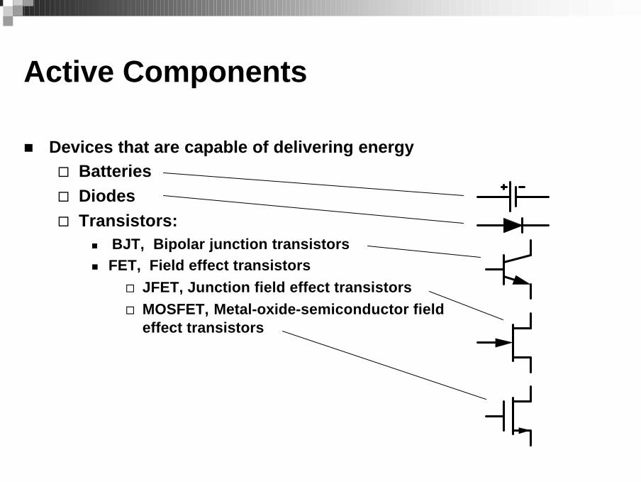
n Devices that are capable of delivering energy¨ Batteries¨ Diodes¨ Transistors:
n BJT, Bipolar junction transistorsn FET, Field effect transistors
¨ JFET, Junction field effect transistors¨ MOSFET, Metal-oxide-semiconductor field
effect transistors

Sensors
MeasurandsForm of signal
Thermal Temperature, heat.
Radiation Gamma rays, X-rays, visible, infrared.
Mechanical Displacement, velocity, force, torque, pressure
Magnetic Magnetic field, flux, magnetic permeability.
Chemical Humidity, pH level, odors, toxics, pollutants.
Biological Sugars, proteins, hormones.
Electrical Charge, resistance, capacitance, frequency.
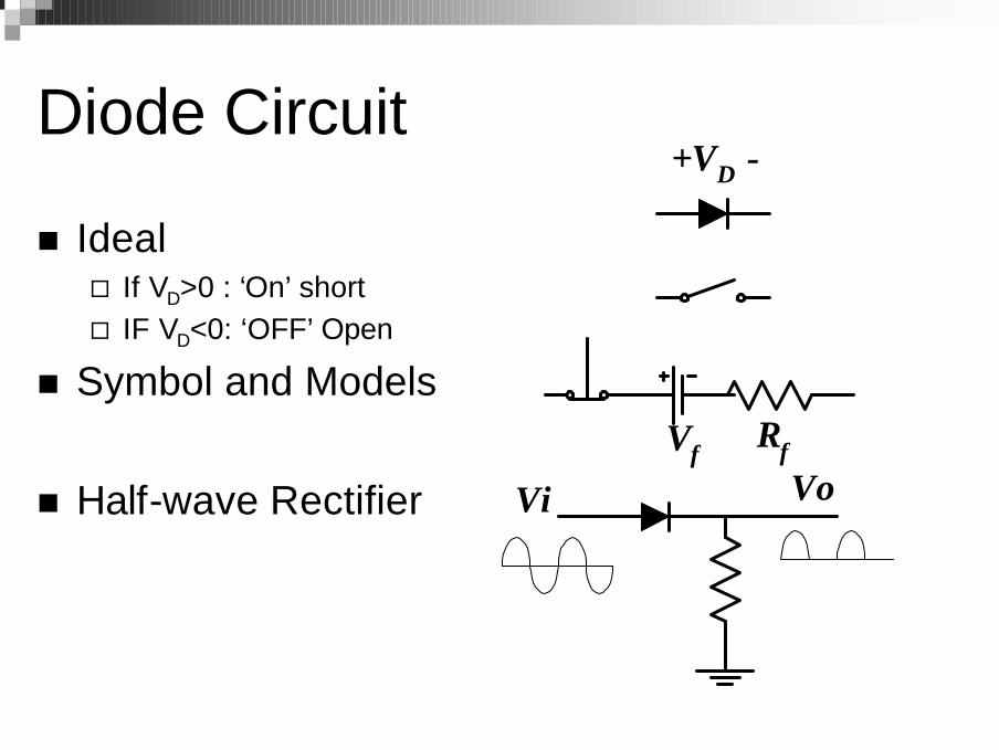
Diode Circuit
n Ideal¨ If VD>0 : ‘On’short¨ IF VD<0: ‘OFF’Open
n Symbol and Models
n Half-wave Rectifier
Rf
+VD -
VfVi Vo
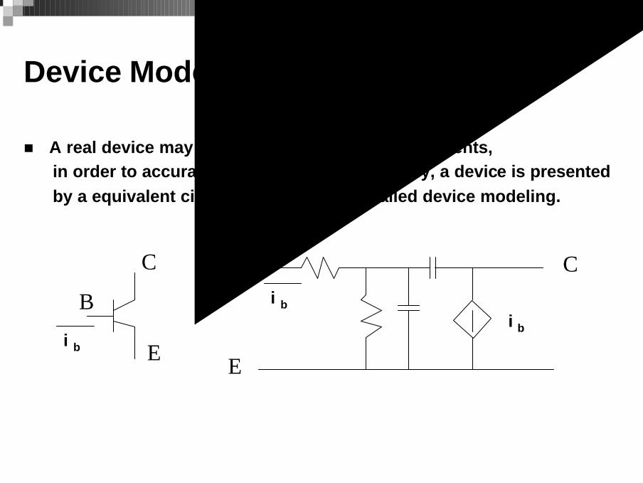
Device Modeling
n A real device may contain many parasitic components,in order to accurately analyze a circuit, usually, a device is presentedby a equivalent circuit. This process is called device modeling.
≡i b
βi bB
C
E
B
E
C
i b
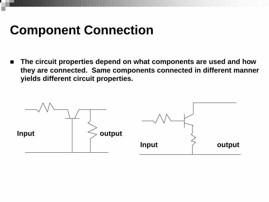
Component Connection
n The circuit properties depend on what components are used and how they are connected. Same components connected in different manner yields different circuit properties.
Input output
Input output
Integrated Circuits
n Most of the electronic systems contains more than one integrated-circuit sub-system.
n Advantages of integration include: miniaturization, improved reliability, increased speed, cost reduction, etc..
n According to application, ICs are categorized into linear (analog) IC, digital IC, and mixed mode IC.
n IC fabrication technology includes: bipolar technology, complementary MOS (CMOS) technology, and BiCMOS technology.
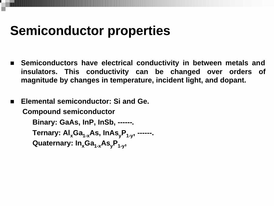
Semiconductor properties
n Semiconductors have electrical conductivity in between metals and insulators. This conductivity can be changed over orders of magnitude by changes in temperature, incident light, and dopant.
n Elemental semiconductor: Si and Ge.Compound semiconductor
Binary: GaAs, InP, InSb, ------.Ternary: AlxGa1-xAs, InAsyP1-y, ------.Quaternary: InxGa1-xAsyP1-y,

Fabrication technologies
n Semiconductor process technologies includes:thermal oxidationdiffusionrapid thermal processingion implantationchemical vapor deposition (CVD)photolithographyetchingmetallizationetc.

Fabrication(Inverter)
Source: Kang’s “CMOS Digital Integrated Circuits Analysis and Design, 2nd Ed. 2000, McGraw-Hall
Vin Vout
Vin Vout
0 11 0
Symbol
Truth Table
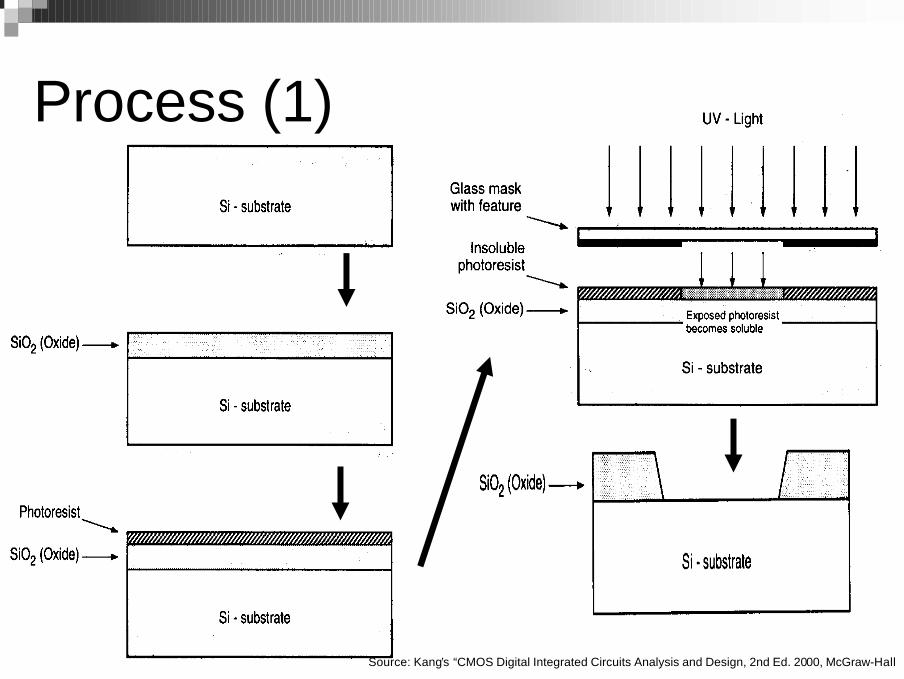
Process (1)
Source: Kang’s “CMOS Digital Integrated Circuits Analysis and Design, 2nd Ed. 2000, McGraw-Hall
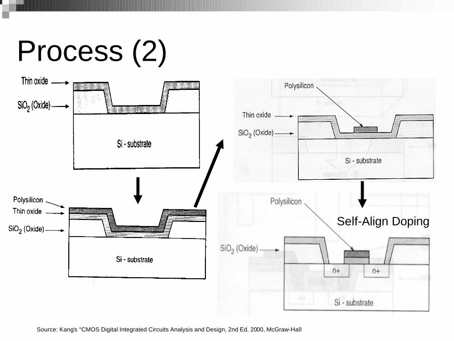
Process (2)
Self-Align Doping
Source: Kang’s “CMOS Digital Integrated Circuits Analysis and Design, 2nd Ed. 2000, McGraw-Hall
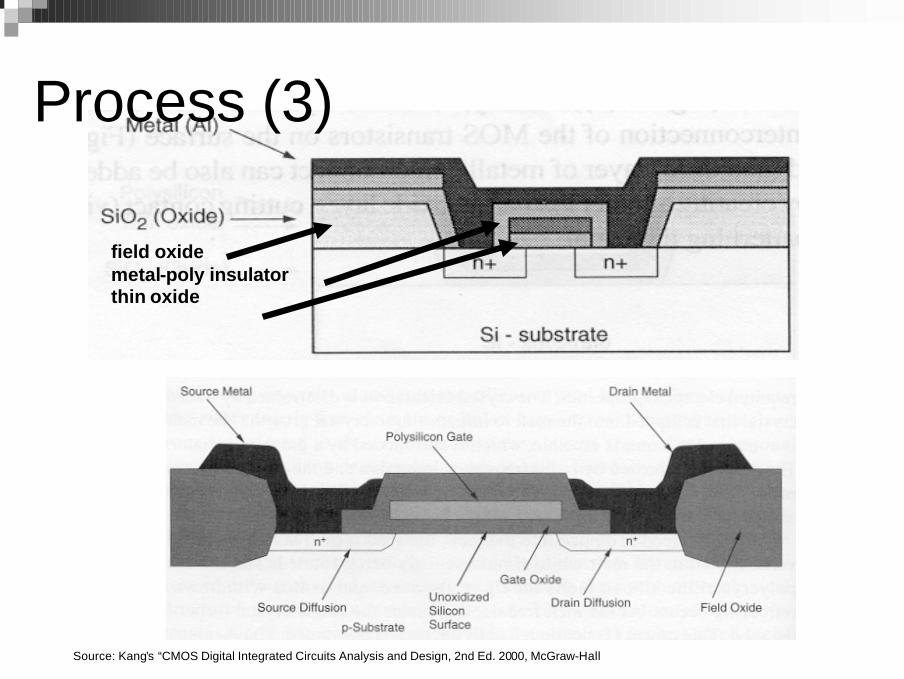
field oxidemetal-poly insulatorthin oxide
Process (3)
Source: Kang’s “CMOS Digital Integrated Circuits Analysis and Design, 2nd Ed. 2000, McGraw-Hall
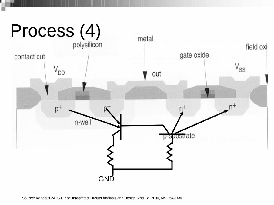
GND
Process (4)
Source: Kang’s “CMOS Digital Integrated Circuits Analysis and Design, 2nd Ed. 2000, McGraw-Hall
Simulation tools
n Process simulationn Device property simulationn Device parameters extractionn Circuit simulationn Layout tools
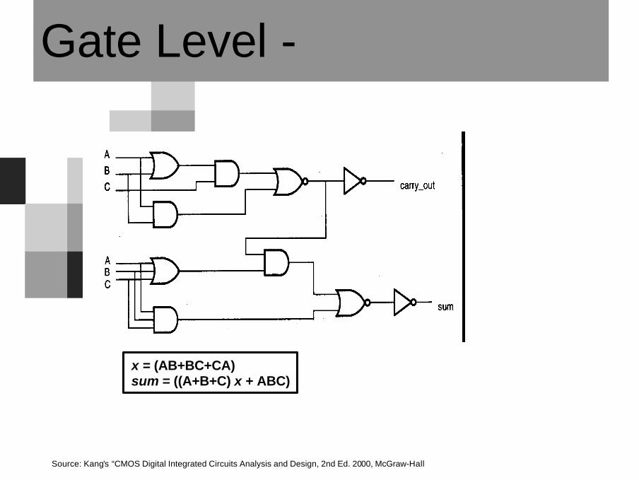
Gate Level - 邏輯設計
Source: Kang’s “CMOS Digital Integrated Circuits Analysis and Design, 2nd Ed. 2000, McGraw-Hall
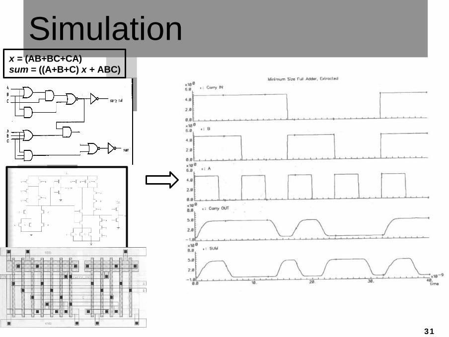
x = (AB+BC+CA)sum = ((A+B+C) x + ABC)

Transistor level -數位電路分析與設計 (電子三)
x
x
Source: Kang’s “CMOS Digital Integrated Circuits Analysis and Design, 2nd Ed. 2000, McGraw-Hall
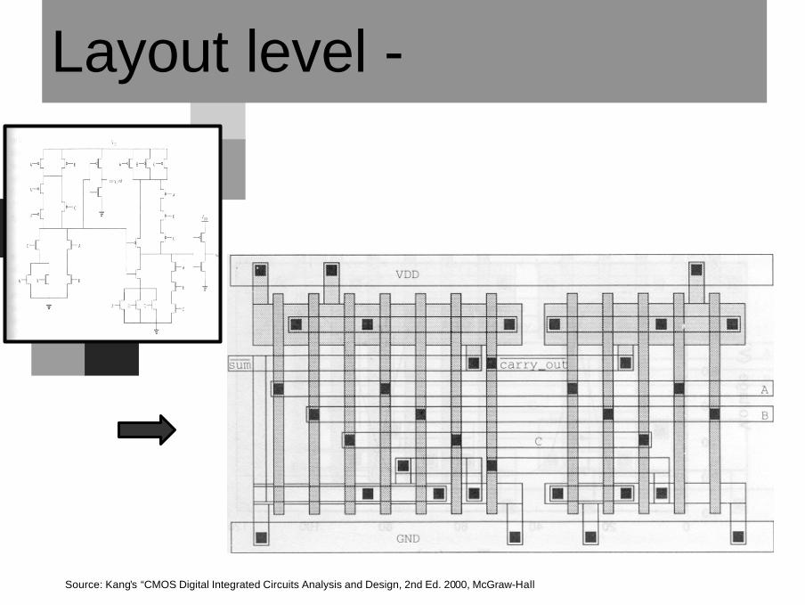
Layout level - 積體電路設計導論
Source: Kang’s “CMOS Digital Integrated Circuits Analysis and Design, 2nd Ed. 2000, McGraw-Hall
31
Simulationx = (AB+BC+CA)sum = ((A+B+C) x + ABC)