lecture 34: designing amplifiers, biasing, frequency responseee105/sp04/handouts/lectures/... ·...
TRANSCRIPT
1
Department of EECS University of California, Berkeley
EECS 105 Spring 2004, Lecture 34
Lecture 34: Designing amplifiers, biasing,
frequency response
Prof J. S. Smith
Department of EECS University of California, Berkeley
EECS 105 Spring 2004, Lecture 34 Prof. J. S. Smith
Context
We will figure out more of the design parameters for the amplifier we looked at in the last lecture, and then we will do a review of the approximate frequency analysis of circuits which have a single dominant pole.

2
Department of EECS University of California, Berkeley
EECS 105 Spring 2004, Lecture 34 Prof. J. S. Smith
Reading
Chapter 9, multi-stage amplifiers. The frequency analysis is in the first section of chapter 10, but we won’t go farther into chapter 10 for a while.
The Lectures on Wednesday and Friday will be given by Joe and Jason, respectively. They will be doing several example problems.
Department of EECS University of California, Berkeley
EECS 105 Spring 2004, Lecture 34 Prof. J. S. Smith
Lecture Outline
Example 1: Cascode Amp DesignExample 2; CS NMOS->CS PMOSReview of frequency analysis (with a dominant pole)

3
Department of EECS University of California, Berkeley
EECS 105 Spring 2004, Lecture 34 Prof. J. S. Smith
Amplifier Schematic
Note that the backgateconnection for M2 is notspecified: ignore gmb
Department of EECS University of California, Berkeley
EECS 105 Spring 2004, Lecture 34 Prof. J. S. Smith
Complete Amplifier Schematic
Goals: gm1 = 1 mS,Rout =10 MΩ
Bias voltagesderived fromtransistors undersimilar operatingconditions tothe transistorsthey supply
Cascode current sourceFor high roc
CS input, with low voltagegain
CG output

4
Department of EECS University of California, Berkeley
EECS 105 Spring 2004, Lecture 34 Prof. J. S. Smith
Current Supply Design
Output resistance goal requires large roc for high gainso we used a cascodecurrent source
High impedance current source means all of thesmall signal current goes to the load resistance,giving more SS voltage gain
Department of EECS University of California, Berkeley
EECS 105 Spring 2004, Lecture 34 Prof. J. S. Smith
Totem Pole Voltage SupplyDC voltages must be set for the cascode current supply transistors M3 and M4, as well as the gate of M2.
M2B supplies the Bias quiescent voltageFor the CG stage
5
Department of EECS University of California, Berkeley
EECS 105 Spring 2004, Lecture 34 Prof. J. S. Smith
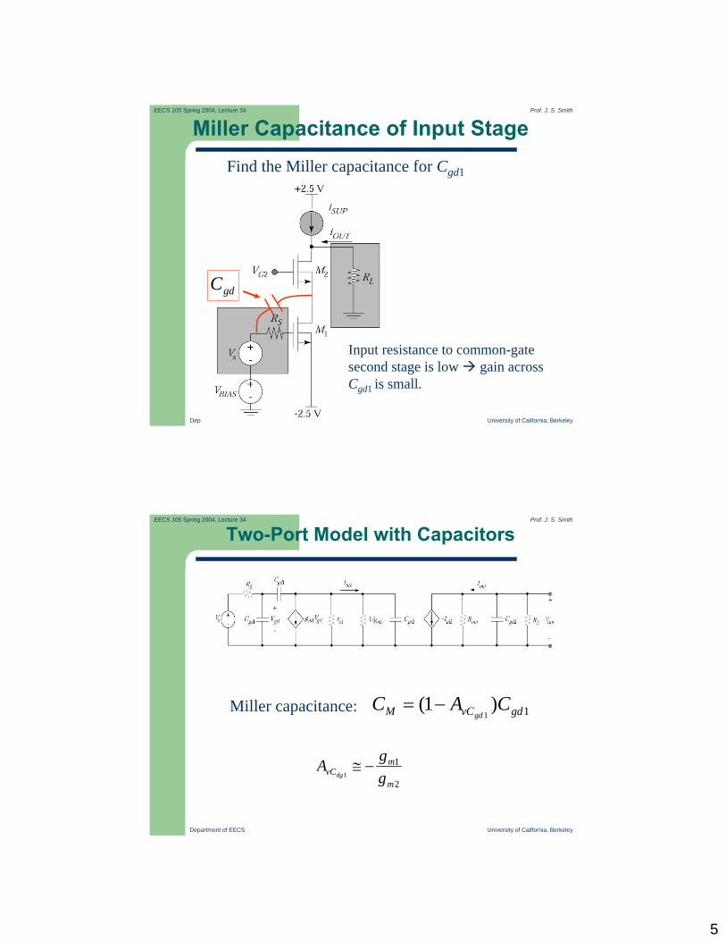
Miller Capacitance of Input StageFind the Miller capacitance for Cgd1
Input resistance to common-gatesecond stage is low gain acrossCgd1 is small.
gdC
Department of EECS University of California, Berkeley
EECS 105 Spring 2004, Lecture 34 Prof. J. S. Smith
Two-Port Model with Capacitors
Miller capacitance: 1)1(1 gdvCM CAC
gd−=
2
11
m
mvC g
gAdg
−≅
6
Department of EECS University of California, Berkeley
EECS 105 Spring 2004, Lecture 34 Prof. J. S. Smith
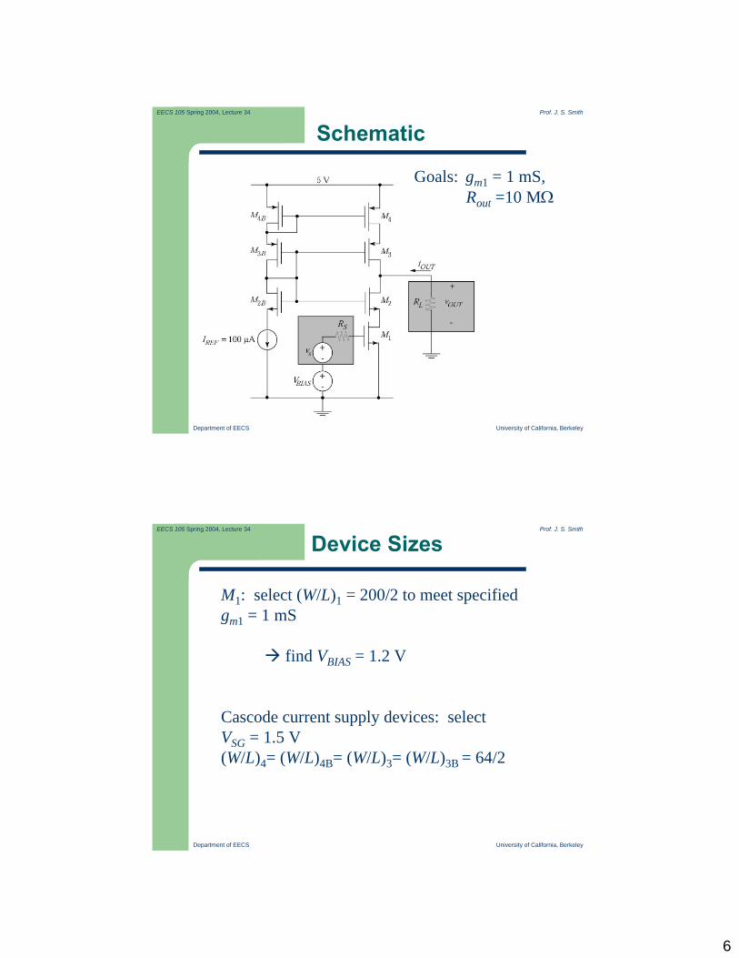
Schematic
Goals: gm1 = 1 mS,Rout =10 MΩ
Department of EECS University of California, Berkeley
EECS 105 Spring 2004, Lecture 34 Prof. J. S. Smith
Device Sizes
M1: select (W/L)1 = 200/2 to meet specified gm1 = 1 mS
find VBIAS = 1.2 V
Cascode current supply devices: select VSG = 1.5 V(W/L)4= (W/L)4B= (W/L)3= (W/L)3B = 64/2

7
Department of EECS University of California, Berkeley
EECS 105 Spring 2004, Lecture 34 Prof. J. S. Smith
Device Sizes
M2: select (W/L)2 = 50/2 to meet specified Rout =10 MΩ
find VGS2 = 1.4 V
Match M2 with diode-connected device M2B.
Assuming perfect matching and zero input voltage,what is VOUT?
Department of EECS University of California, Berkeley
EECS 105 Spring 2004, Lecture 34 Prof. J. S. Smith
Output (Voltage) Swing
Maximum VOUT
Minimum VOUT
8
Department of EECS University of California, Berkeley
EECS 105 Spring 2004, Lecture 34 Prof. J. S. Smith
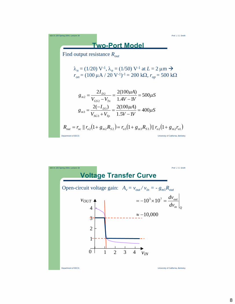
Two-Port ModelFind output resistance Rout
λn = (1/20) V-1, λn = (1/50) V-1 at L = 2 µm ron = (100 µA / 20 V-1)-1 = 200 kΩ, rop = 500 kΩ
( ) ( ) ( )122333222 1||11|| omoSmoSmoocout rgrRgrRgrrR ++=+=
SVVA
VVIg
TnGS
Dm µµ 500
14.1)100(22
2
22 =
−=
−=
SVVA
VVIg
TpSG
Dm µµ 400
15.1)100(2)(2
3
33 =
−=
+−
=
Department of EECS University of California, Berkeley
EECS 105 Spring 2004, Lecture 34 Prof. J. S. Smith
Voltage Transfer CurveOpen-circuit voltage gain: Av = vout / vin = - gm1Rout
vOUT
vIN
3
4
1
2 1 0 3 4
2
000,10
1010 73
−≈
=×−=Qin
out
dvdv

9
Department of EECS University of California, Berkeley
EECS 105 Spring 2004, Lecture 34 Prof. J. S. Smith
Multistage Amplifier Design Example
Start with basic two-stage transconductance amplifier:
Why do this combination?
Department of EECS University of California, Berkeley
EECS 105 Spring 2004, Lecture 34 Prof. J. S. Smith
Quiescent level shifts
PMOSNMOS
⇑(known shift)
⇓(known shift)
CD
Source follower
⇓⇑CG
⇓(typical)
⇑(typical)
CS

10
Department of EECS University of California, Berkeley
EECS 105 Spring 2004, Lecture 34 Prof. J. S. Smith
CS→CS Amplifier
Direct DC connection: use NMOS then PMOS
Department of EECS University of California, Berkeley
EECS 105 Spring 2004, Lecture 34 Prof. J. S. Smith
Current Supply Design
Assume that the reference is a “sink” set by a resistor
Must mirror the reference current and generate a sink for iSUP 2
11
Department of EECS University of California, Berkeley
EECS 105 Spring 2004, Lecture 34 Prof. J. S. Smith
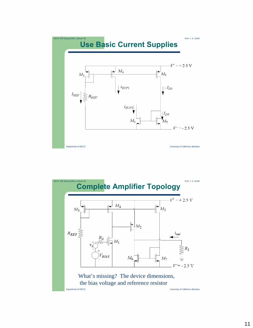
Use Basic Current Supplies
Department of EECS University of California, Berkeley
EECS 105 Spring 2004, Lecture 34 Prof. J. S. Smith
Complete Amplifier Topology
What’s missing? The device dimensions,the bias voltage and reference resistor

12
Department of EECS University of California, Berkeley
EECS 105 Spring 2004, Lecture 34 Prof. J. S. Smith
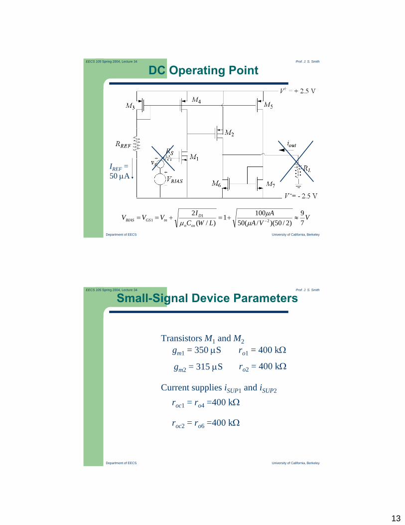
DC Bias: Find Operating Points
Find VBIAS such that VOUT = 0 VDevice parameters:
=oxnCµ 50 µA/V2 =oxpCµ 25 µA/V2
λn = 0.05 V-1 λp = 0.05 V-1
VTn = 1 V VTp = -1 V
Device dimensions (for “lecture” design):
(W/L)n = 50/2 (W/L)p = 80/2
Department of EECS University of California, Berkeley
EECS 105 Spring 2004, Lecture 34 Prof. J. S. Smith
Finding RREF
V+ V+
V-
RREF
M3
Require IREF = - ID3 = 50 µA
3
33 )/(
2LWC
IVVoxp
DTpSG µ
−+−=
[ ] [ ]ref
SGREF R
VVVAI−+ −−
== 350µ
VA
AVVSG 32.14041
)2/80(25502)1(3 =+=
×−+−−=
µµ
[ ] [ ]Ω=⇒
−−−= kR
RA ref
ref
745.232.15.250µ
13
Department of EECS University of California, Berkeley
EECS 105 Spring 2004, Lecture 34 Prof. J. S. Smith
DC Operating Point
IREF =50 µA
VVA
ALWC
IVVVoxn
DtnGSBIAS 7
9)2/50)(/(50
1001)/(
22
11 ≈+=+== −µ
µµ
Department of EECS University of California, Berkeley
EECS 105 Spring 2004, Lecture 34 Prof. J. S. Smith
Small-Signal Device Parameters
gm1 = 350 µS
gm2 = 315 µS
ro1 = 400 kΩ
ro2 = 400 kΩ
Transistors M1 and M2
Current supplies iSUP1 and iSUP2
roc1 = ro4 =400 kΩ
roc2 = ro6 =400 kΩ
14
Department of EECS University of California, Berkeley
EECS 105 Spring 2004, Lecture 34 Prof. J. S. Smith
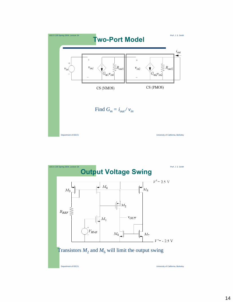
Two-Port Model
Find Gm = iout / vin
Department of EECS University of California, Berkeley
EECS 105 Spring 2004, Lecture 34 Prof. J. S. Smith
Output Voltage Swing
Transistors M2 and M6 will limit the output swing
15
Department of EECS University of California, Berkeley
EECS 105 Spring 2004, Lecture 34 Prof. J. S. Smith
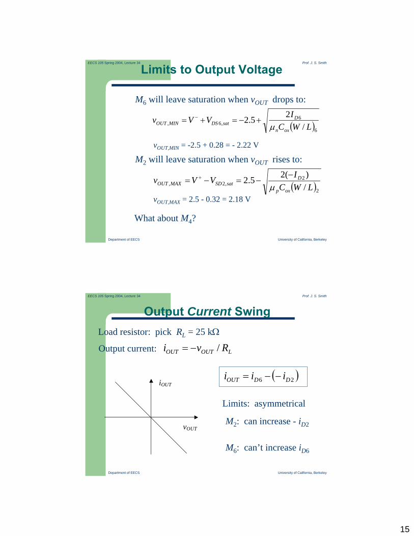
Limits to Output Voltage
M6 will leave saturation when vOUT drops to:
( )66
,6, /25.2
LWCIVVv
oxn
DsatDSMINOUT µ
+−=+= −
M2 will leave saturation when vOUT rises to:
( )22
,2, /)(25.2LWC
IVVvoxp
DsatSDMAXOUT µ
−−=−= +
What about M4?
vOUT,MIN = -2.5 + 0.28 = - 2.22 V
vOUT,MAX = 2.5 - 0.32 = 2.18 V
Department of EECS University of California, Berkeley
EECS 105 Spring 2004, Lecture 34 Prof. J. S. Smith
Output Current SwingLoad resistor: pick RL = 25 kΩ
Output current: LOUTOUT Rvi /−=
iOUT
vOUT
Limits: asymmetrical
M2: can increase - iD2
M6: can’t increase iD6
( )26 DDOUT iii −−=

16
Department of EECS University of California, Berkeley
EECS 105 Spring 2004, Lecture 34 Prof. J. S. Smith
Output Current Limits• Positive output current (negative vOUT)
( ) LMINOUTDMAXOUT RvAii /500 ,6, −==−= µ
• Negative output current (positive vOUT)
VkAv MINOUT 25.1)25)(50(, −=Ω−= µ(less negative than limit set by saturation of M6)
No limit on current from M2, so voltage swing setscurrent limit
AkV
Rvi LMAXOUTMINOUT
µ2.87)25/18.2(
/,,
−=Ω−
=−=
Department of EECS University of California, Berkeley
EECS 105 Spring 2004, Lecture 34 Prof. J. S. Smith
Transfer Curves (for RL = 25 kΩ)
vOUT
vIN
1
2
-1
-2
0 -1 -2 1 2
iOUT [µA]
vIN
50
100
-50
-100
0 -1 -2 1 2
Loaded voltage gain = vout/vin = (gm1Rout1)(gm2Rout||RL) = 490
Loaded transconductance = iout/vin= (-gm1Rout1)(gm2)(Rout/(Rout + RL) = -19.5 mS

17
Department of EECS University of California, Berkeley
EECS 105 Spring 2004, Lecture 34 Prof. J. S. Smith
Review: Frequency Resp of Multistage Amplifiers
• We have a systematic technique to study amplifier performance (derive transfer function, study poles/zeros/Bode pltos).
• In most cases, the systematic approach is too cumbersome.
• We have a good qualitative understanding of circuit performance (e.g., CS suffers from Miller effect, CD andd CG are wideband stages …)
• Open Circuit Time Constants: Analytical technique is capable of estimating only the dominant (lowest) pole …for a restricted class of amplifiers.
Department of EECS University of California, Berkeley
EECS 105 Spring 2004, Lecture 34 Prof. J. S. Smith
The Special CaseThe transfer function can have no zeroes and must have a dominant pole ω1 << ω2, ω3, …, ωn
( )...)()(1)(
33
22
1 ++++=
bjbjbjHjH o
ωωωω
( )( ) ( )n
o
jjjHjH
ωωωωωωω
/1.../1/1)(
21 +++=
Factor denominator:

18
Department of EECS University of California, Berkeley
EECS 105 Spring 2004, Lecture 34 Prof. J. S. Smith
Approximating the Transfer FunctionMultiply out denominator:
( )( ) ( )n
o
jjjHjH
ωωωωωωω
/1.../1/1)(
21 +++=
⎟⎟⎠
⎞⎜⎜⎝
⎛++++
≈
n
o
j
H
ωωωω 1...111
21
Since ω1 << ω2, ω3, …, ωn
1211
11...11ωωωω
≈+++=n
b
Department of EECS University of California, Berkeley
EECS 105 Spring 2004, Lecture 34 Prof. J. S. Smith
How to Find b1?See P. R. Gray and R. G. Meyer, Analysis and Design of
Analog Integrated Circuits (EE 140) for derivation
Result: b1 is the sum of open-circuit time constantsτi which can be found by considering each capacitor Ci in the amplifier separately andfinding the Thévenin resistance RTi of thenetwork from the capacitor’s point ofview τi = RTi Ci
∑∑
=
=≈⎯→⎯= n
i iTi
n
i iTiCR
CRb1
1111ω

19
Department of EECS University of California, Berkeley
EECS 105 Spring 2004, Lecture 34 Prof. J. S. Smith
Finding the Thévenin Resistance
1. Open-circuit all capacitors (i.e.; remove them)
2. For capacitor Ci, find the resistance RTi across itsterminals with all independent sources removed(voltages shorted, currents opened) … might needto apply a test voltage and find the current in somecases.
Insight for design: the bandwidth of the amplifier willbe limited by the capacitor that contributes the largestτi = RTi Ci not necessarily the largest Ci