lecture 16: semiconductors (kittel ch. 8)
TRANSCRIPT
Physics 460 F 2006 Lect 16 1
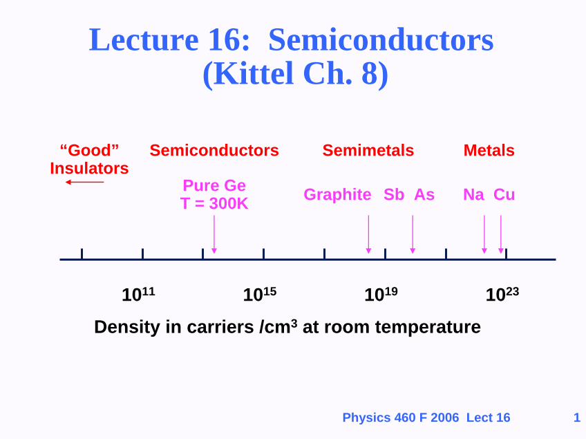
Lecture 16: Semiconductors (Kittel Ch. 8)
“Good”Insulators
Semiconductors Semimetals Metals
Pure GeT = 300K Graphite Sb As Na Cu
1011 1015 1019 1023
Density in carriers /cm3 at room temperature
Physics 460 F 2006 Lect 16 2
Outline• What is a semiconductor?
• Bands in real semiconductors - Si, Ge, GaAs, ... Starting point - Nearly free electrons!Energy gaps
• Optical propertiesWhy is GaAs so different from Si and Ge?
• (Read Kittel Ch 8)
Physics 460 F 2006 Lect 16 3
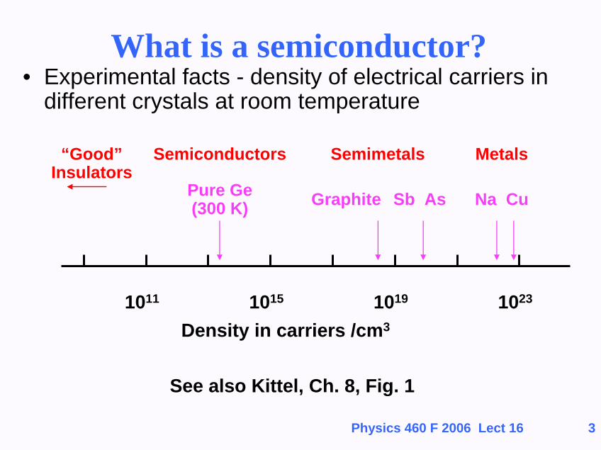
What is a semiconductor?• Experimental facts - density of electrical carriers in
different crystals at room temperature
“Good”Insulators
Semiconductors Semimetals Metals
Pure Ge(300 K) Graphite Sb As Na Cu
1011 1015 1019 1023
Density in carriers /cm3
See also Kittel, Ch. 8, Fig. 1

Physics 460 F 2006 Lect 16 4
What is a semiconductor?• Experimental facts - temperature dependence of
carrier concentration indicates an energy gap
1010
1011
1012
1013
Den
sity
in c
arrie
rs /c
m3
Pure Ge
n ∝ exp(-Egap/kB T)
See Kittel, Ch. 8, Fig. 3
200 K T 300 K
Physics 460 F 2006 Lect 16 5
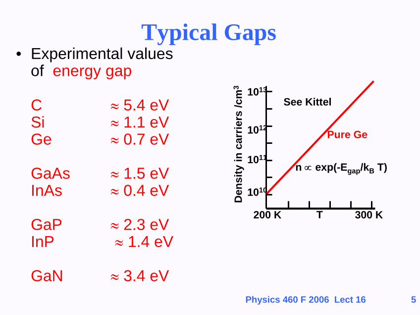
Typical Gaps• Experimental values
of energy gap
C ≈ 5.4 eV Si ≈ 1.1 eVGe ≈ 0.7 eV
GaAs ≈ 1.5 eV InAs ≈ 0.4 eV
GaP ≈ 2.3 eVInP ≈ 1.4 eV
GaN ≈ 3.4 eV
1010
1011
1012
1013
Den
sity
in c
arrie
rs /c
m3
200 K 300 KT
Pure Ge
n ∝ exp(-Egap/kB T)
See Kittel

Physics 460 F 2006 Lect 16 6
What is a semiconductor?• Experimental facts:
Carrier concentration varies dramatically with purity(Can be changed or controlled - unlike a good metal like Cu)
Carriers can have different signs! Positive and negative - as shown by Hall effect
• How can all this happen?
Interpretation in terms of electron bands?

Physics 460 F 2006 Lect 16 7
Metals vs Insulators • A band holds two electrons per cell of the crystal • Therefore an crystal with an odd number of electrons
per cell MUST* be a metal!Partially filled bands lead to Fermi energy and
“Fermi surface” in k spaceConductivity because states can change and
scatter when electric field is applied
• A crystal with an even number of electrons per cell MAY be an insulator!
Electrons “frozen”Gap in energy for any excitations of electrons
From last time
Physics 460 F 2006 Lect 16 8
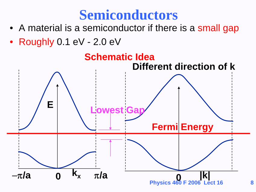
Semiconductors • A material is a semiconductor if there is a small gap• Roughly 0.1 eV - 2.0 eV
E
kx π/a−π/a 0 0 |k|
Different direction of k
Fermi Energy
Lowest Gap
Schematic Idea

Physics 460 F 2006 Lect 16 9
Semimetals (close relative) • Small changes in the bands leads to “band overlap”,
which has relations to what happens in a semiconductor
E
kx π/a−π/a 0 0 |k|
Different direction of k
Fermi Energy
Empty statesFilled states
Physics 460 F 2006 Lect 16 10
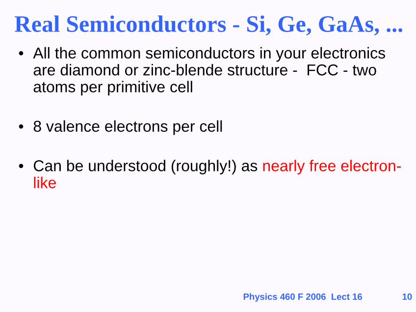
Real Semiconductors - Si, Ge, GaAs, ... • All the common semiconductors in your electronics
are diamond or zinc-blende structure - FCC - two atoms per primitive cell
• 8 valence electrons per cell
• Can be understood (roughly!) as nearly free electron-like
Physics 460 F 2006 Lect 16 11
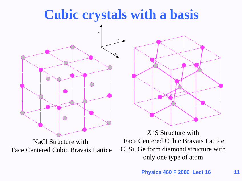
Cubic crystals with a basis
NaCl Structure with Face Centered Cubic Bravais Lattice
X
y
z
ZnS Structure with Face Centered Cubic Bravais Lattice
C, Si, Ge form diamond structure with only one type of atom

Physics 460 F 2006 Lect 16 12
(110) plane in diamond structure crystal
(100) plane in ZnS crystalzig-zag Zn-S chains of atoms
(diamond if the two atoms are the same)
X
y
z
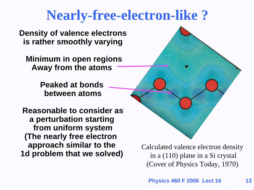
Calculated valence electron density in a (110) plane in a Si crystal
(Cover of Physics Today, 1970)
Physics 460 F 2006 Lect 16 13
Nearly-free-electron-like ?
Calculated valence electron density in a (110) plane in a Si crystal
(Cover of Physics Today, 1970)
Density of valence electronsis rather smoothly varying
Minimum in open regionsAway from the atoms
Peaked at bonds between atoms
Reasonable to consider asa perturbation starting from uniform system
(The nearly free electron approach similar to the
1d problem that we solved)
Physics 460 F 2006 Lect 16 14
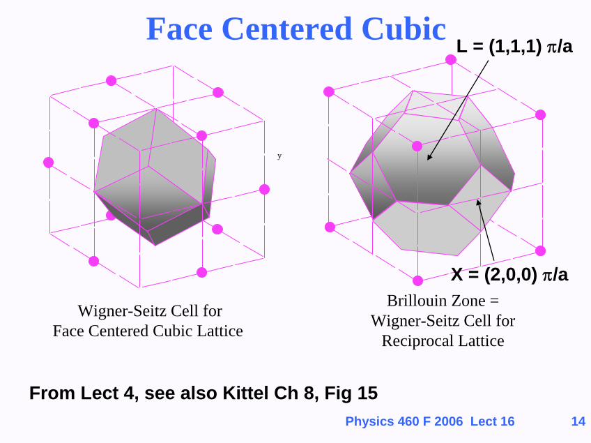
Wigner-Seitz Cell forFace Centered Cubic Lattice
Brillouin Zone =Wigner-Seitz Cell for
Reciprocal Lattice
y
X = (2,0,0) π/a
L = (1,1,1) π/aFace Centered Cubic
From Lect 4, see also Kittel Ch 8, Fig 15
Physics 460 F 2006 Lect 16 15
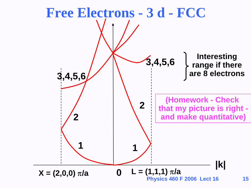
Free Electrons - 3 d - FCC
2
|k|L = (1,1,1) π/a0
1
3,4,5,63,4,5,6
2
1
Interestingrange if there
are 8 electrons
(Homework - Check that my picture is right -and make quantitative)
X = (2,0,0) π/a
Physics 460 F 2006 Lect 16 16
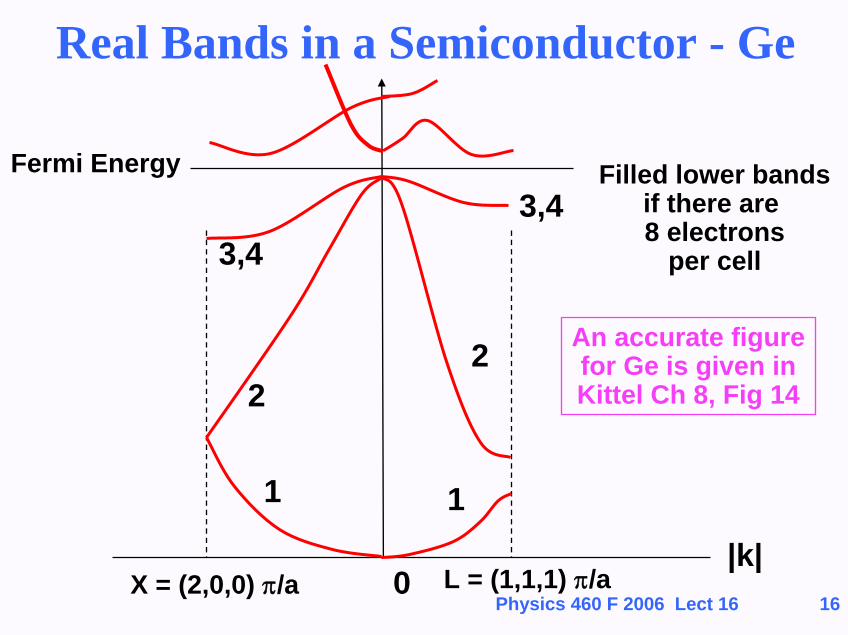
Real Bands in a Semiconductor - Ge
2
|k|L = (1,1,1) π/aX = (2,0,0) π/a 0
1
3,43,4
2
1
Filled lower bandsif there are 8 electrons
per cell
Fermi Energy
An accurate figurefor Ge is given inKittel Ch 8, Fig 14
Physics 460 F 2006 Lect 16 17
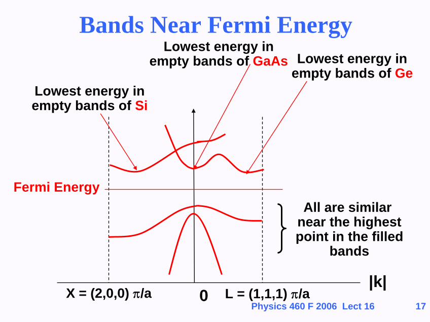
Bands Near Fermi EnergyLowest energy in
empty bands of Ge
Lowest energy inempty bands of GaAs
Lowest energy inempty bands of Si
Fermi EnergyAll are similar
near the highestpoint in the filled
bands
|k|X = (2,0,0) π/a L = (1,1,1) π/a0
Physics 460 F 2006 Lect 16 18
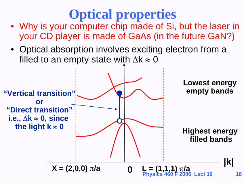
Optical properties
|k|L = (1,1,1) π/aX = (2,0,0) π/a 0
Lowest energyempty bands
• Why is your computer chip made of Si, but the laser in your CD player is made of GaAs (in the future GaN?)
• Optical absorption involves exciting electron from a filled to an empty state with ∆k ≈ 0
Highest energy filled bands
“Vertical transition”or
“Direct transition”i.e., ∆k ≈ 0, since
the light k ≈ 0
Physics 460 F 2006 Lect 16 19
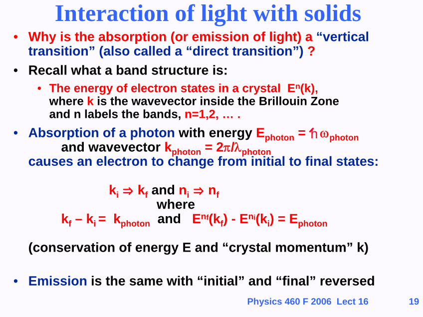
Interaction of light with solids• Why is the absorption (or emission of light) a “vertical
transition” (also called a “direct transition”) ?• Recall what a band structure is:
• The energy of electron states in a crystal En(k),where k is the wavevector inside the Brillouin Zoneand n labels the bands, n=1,2, … .
• Absorption of a photon with energy Ephoton = ωphotonand wavevector kphoton = 2π/λphoton
causes an electron to change from initial to final states:
ki fi kf and ni fi nfwhere
kf – ki = kphoton and Enf(kf) - Eni(ki) = Ephoton
(conservation of energy E and “crystal momentum” k)
• Emission is the same with “initial” and “final” reversed
h
Physics 460 F 2006 Lect 16 20
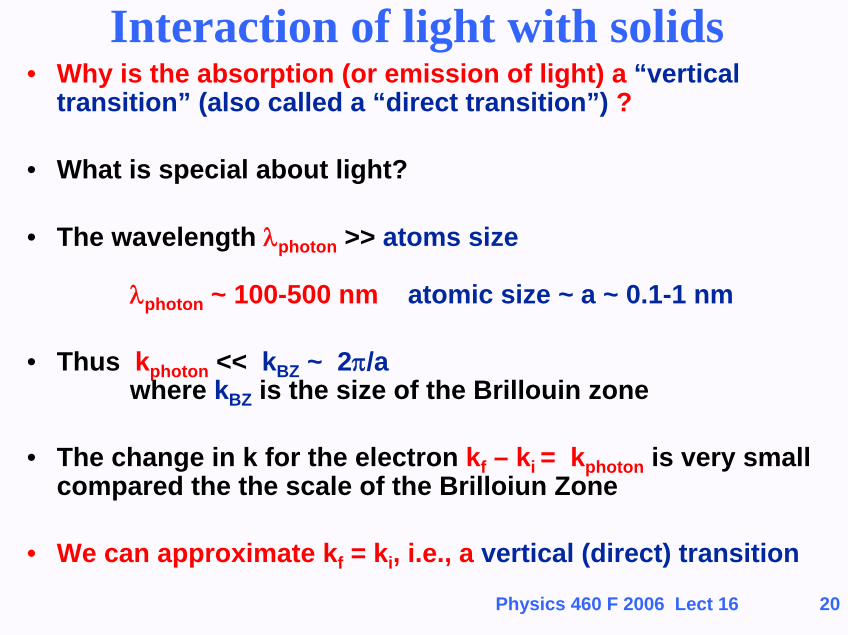
Interaction of light with solids• Why is the absorption (or emission of light) a “vertical
transition” (also called a “direct transition”) ?
• What is special about light?
• The wavelength λphoton >> atoms size
λphoton ~ 100-500 nm atomic size ~ a ~ 0.1-1 nm
• Thus kphoton << kBZ ~ 2π/awhere kBZ is the size of the Brillouin zone
• The change in k for the electron kf – ki = kphoton is very small compared the the scale of the Brilloiun Zone
• We can approximate kf = ki, i.e., a vertical (direct) transition
Physics 460 F 2006 Lect 16 21
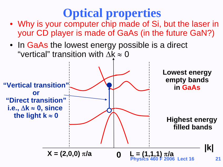
Optical properties
|k|L = (1,1,1) π/aX = (2,0,0) π/a 0
• Why is your computer chip made of Si, but the laser in your CD player is made of GaAs (in the future GaN?)
• In GaAs the lowest energy possible is a direct “vertical” transition with ∆k ≈ 0
Highest energy filled bands
“Vertical transition”or
“Direct transition”i.e., ∆k ≈ 0, since
the light k ≈ 0
Lowest energyempty bands
in GaAs
Physics 460 F 2006 Lect 16 22
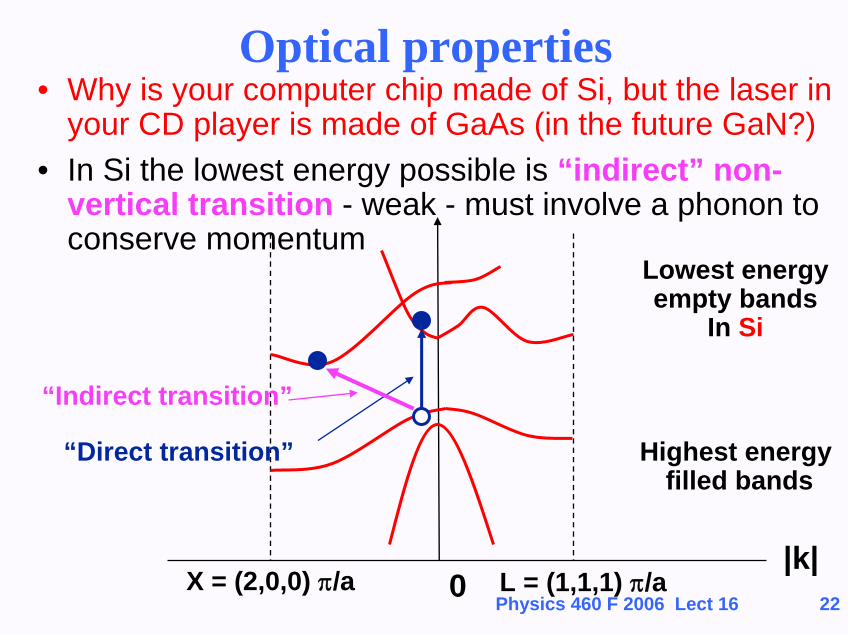
Optical properties
|k|L = (1,1,1) π/aX = (2,0,0) π/a 0
Lowest energyempty bands
In Si
• Why is your computer chip made of Si, but the laser in your CD player is made of GaAs (in the future GaN?)
• In Si the lowest energy possible is “indirect” non-vertical transition - weak - must involve a phonon to conserve momentum
Highest energy filled bands
“Direct transition”
“Indirect transition”
Physics 460 F 2006 Lect 16 23
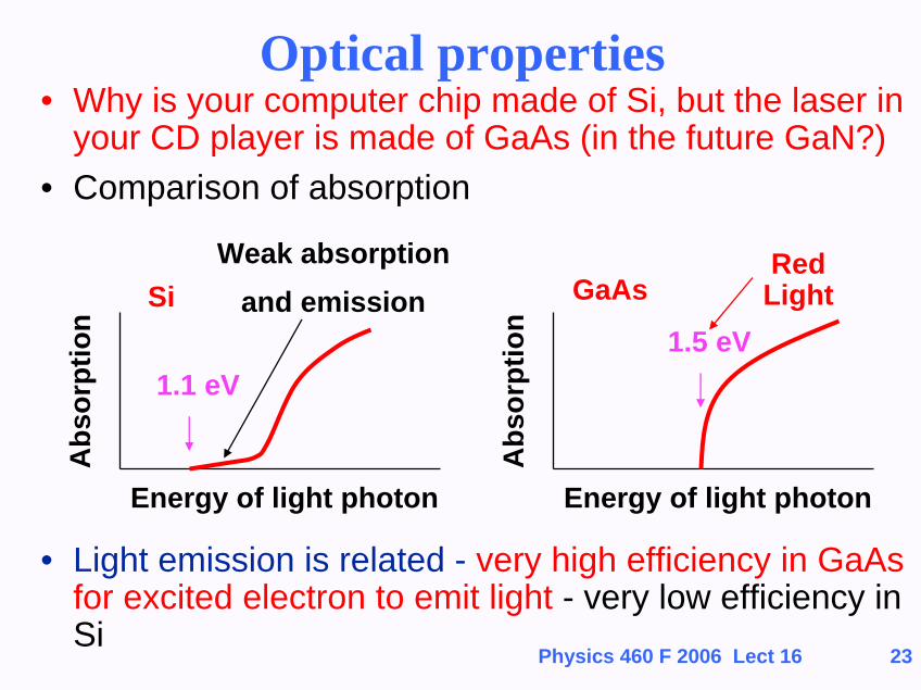
Optical properties• Why is your computer chip made of Si, but the laser in
your CD player is made of GaAs (in the future GaN?)• Comparison of absorption
Energy of light photon
Abs
orpt
ion
Energy of light photonA
bsor
ptio
n
GaAsSi
1.1 eV1.5 eV
RedLight
Weak absorptionand emission
• Light emission is related - very high efficiency in GaAs for excited electron to emit light - very low efficiency in Si
Physics 460 F 2006 Lect 16 24
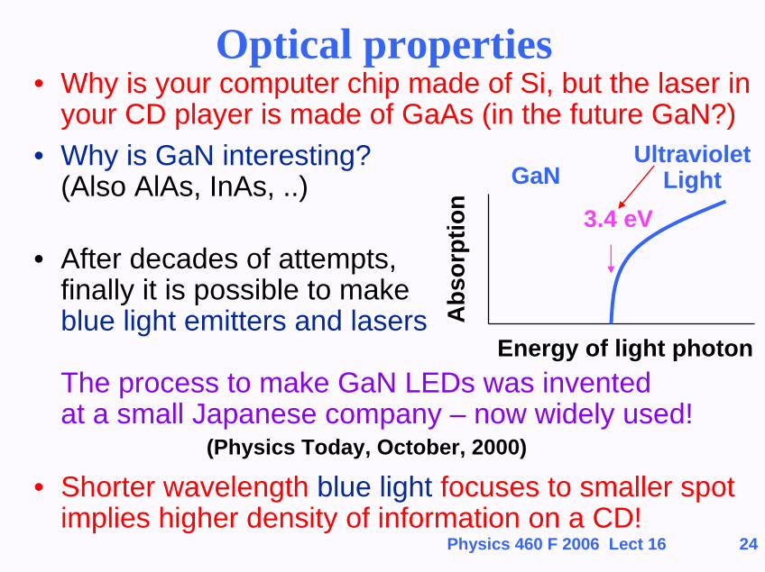
Optical properties• Why is your computer chip made of Si, but the laser in
your CD player is made of GaAs (in the future GaN?)• Why is GaN interesting?
(Also AlAs, InAs, ..)
• After decades of attempts,finally it is possible to makeblue light emitters and lasers
The process to make GaN LEDs was inventedat a small Japanese company – now widely used!
(Physics Today, October, 2000)
Energy of light photon
Abs
orpt
ion
GaN
3.4 eV
UltravioletLight
• Shorter wavelength blue light focuses to smaller spotimplies higher density of information on a CD!
Physics 460 F 2006 Lect 16 25
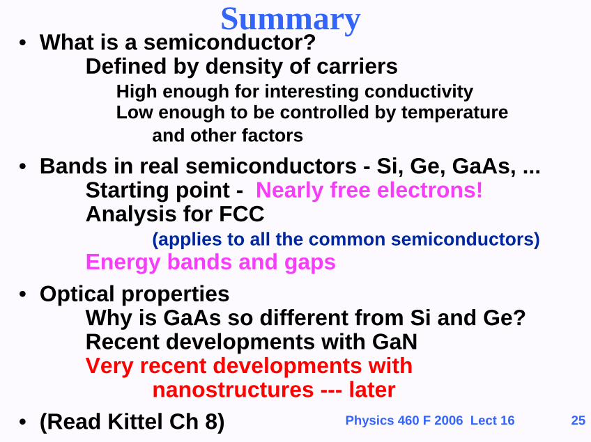
Summary• What is a semiconductor?
Defined by density of carriers High enough for interesting conductivityLow enough to be controlled by temperature
and other factors• Bands in real semiconductors - Si, Ge, GaAs, ...
Starting point - Nearly free electrons!Analysis for FCC
(applies to all the common semiconductors)Energy bands and gaps
• Optical propertiesWhy is GaAs so different from Si and Ge?Recent developments with GaNVery recent developments with
nanostructures --- later • (Read Kittel Ch 8)
Physics 460 F 2006 Lect 16 26
Next time• More en electrons in Semiconductors
Effective massElectrons and holes
• Intrinsic effects in a pure material
• Control of conductivity by doping (impurities)
• (Read Kittel Ch 8)