lecture 16 - course review
TRANSCRIPT

• Lab 7 turn in: Please turn in Lab 7 during the first hour or your usual lab session during finals week
Wed 19th 12-1pmWed 19th 7-8pmThurs 20th 12-1pm
If you cannot make your usual time, hand it in at one of the other session time and let the TAs know
• During these times all 6 TAs will be there for office hours
• My office hours will remain in Finals week – email for appointment if you need to meet at other times
• Wk10 Discussion solution are on the class website

• Please arrive on time!
• Bring cheat-sheet, updated after the quizzes. (VT, stability equations, etc , etc)Hand written or printed ok, 2 sides of 1 sheet of paper.
• You can bring the printed AmpSummary sheet (2 pages) in addition to this.
• Bring calculator
• Look at / do the practice final, go over the quizzes. Go over at least some problems from all of the “Additional Course notes”
• Use recipes for solving circuits
• Quizzes and the practice final are a very good guide (6 questions, 3 hours)
• Topics not on the final: Derivation of pn junction current from semi-conductor physicsMulti-stage amplifier circuits
Suggestions for the final – Thursday 20th March 7-10pm, Ctr Hall 101

ECE65 Course Summary
ECE 65, Winter2014, S. Bott-Suzuki

Devices
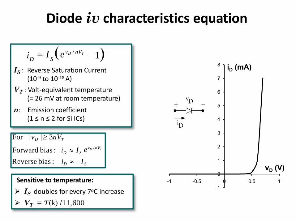
Diode iv characteristics equation
IS : Reverse Saturation Current (10-9 to 10-18 A)
VT : Volt-equivalent temperature(= 26 mV at room temperature)
n: Emission coefficient(1 ≤ n ≤ 2 for Si ICs)
For | vD |≥ 3nVT
= I (evD / nVT −1)D Si
Reverse bias : iD ≈ − I S
Sensitive to temperature: IS doubles for every 7oC increase VT = T(k) /11,600
Forward bias : iD ≈ I S evD / nVT

Diode piecewise-linear model: Diode iv is approximated by two lines
Constant Voltage Model
"cut - in" voltage, VD0 = 0.6 − 0.7 V for Si
OFF:
and iD ≥ 0and vD <VD0
vD =VD0
iD = 0
Diode ON :Diode OFF :
Circuit Models:
ON:
Diode ON
Diode OFF
VD0
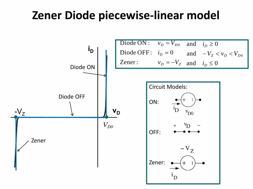
Zener Diode piecewise-linear model
and iD ≥ 0and −VZ < vD <VD0
and iD ≤ 0
Diode ON :Diode OFF :Zener :
vD =VD0
iD = 0vD = −VZDiode ON
Diode OFF
VD0
Zener
Circuit Models:
ON:
OFF:
Zener:

Recipe for solving diode circuits
Recipe:
1. Draw a circuit for each state of diode(s).
2. Solve each circuit with its corresponding diode equation.
3. Use the inequality for that diode state (“range of validity”) to check:o if the solution is valid if circuit parameters are all known.o to find the range of circuit “variable” which leads to that
state.

Accuracy of Constant-Voltage Model
Constant VoltageModel Diode ON
Diode OFF
VD0
Diode can be in forward bias with vD as small as 0.4 V when iD is small (Lab 4)
In forward bias, “cut-in” voltage (VD0) can vary between 0.6 & 0.8 V (± 0.1 V)
In forward bias, diode voltage changesslightly as current changes

BJT iv characteristics includes four parameters
BC is reverse biased
(Deep) Saturation:
CE += v /V
NPN transistor
iB = e
Two transistor parameters can be written in terms of the other four:
KCL : iE = iC + iB
KVL: vBC = vBE − vCE
BJT iv characteristics equations are:iB = f (vBE )iC = g (iB ,vCE )
Cut-off : i = 0, i = 0BE is reverse biased B C
i = iC = IS evBE /VT
Active: B β βBE is forward biased
v i I e BE T 1C S
VA
IS v /VBE T
BE is forward biased βBC is foward biased vCE ≈Vsat , iC < β iB
Arrow on the emitter
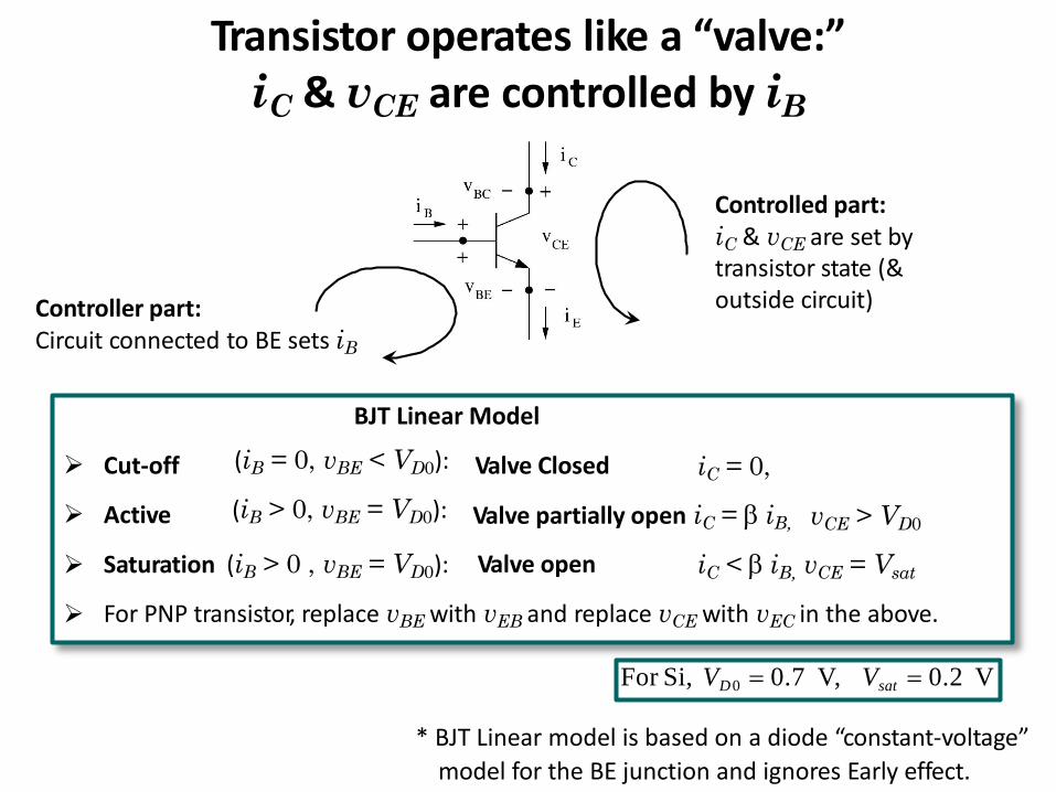
Transistor operates like a “valve:”iC & vCE are controlled by iB
Controller part:Circuit connected to BE sets iB
Controlled part:iC & vCE are set bytransistor state (& outside circuit)
BJT Linear Model
Cut-off
Active
(iB = 0, vBE < VD0):
(iB > 0, vBE = VD0):
Valve Closed iC = 0,
Valve partially open iC = β iB, vCE > VD0
Saturation (iB > 0 , vBE = VD0): Valve open iC < β iB, vCE = Vsat
For PNP transistor, replace vBE with vEB and replace vCE with vEC in the above.
For Si, VD0 = 0.7 V, Vsat = 0.2 V
* BJT Linear model is based on a diode “constant-voltage”model for the BE junction and ignores Early effect.

Recipe for solving BJT circuits(State of BJT is unknown before solving the circuit)
1. Write down BE-KVL and CE-KVL (check for NPN/PNP!):
2. Assume BJT is OFF, Use BE-KVL to check:a. BJT OFF: Set iC = 0, use CE-KVL to find vCE (Done!)b. BJT ON: Compute iB
3. Assume BJT in active. Set iC = β iB . Use CE-KVL to find vCE .If vCE ≥ VD0 , Assumption Correct, otherwise in saturation:
4. BJT in Saturation. Set vCE = Vsat . Use CE-KVL to find iC . (Double-check iC < β iB )
NOTE:o For circuits with RE , both BE-KVL & CE-KVL have to be solved
simultaneously.

MOS i-v Characteristics Equations
NMOS (VOV = vGS – Vtn)
o For PMOS set VOV = vSG – |Vtp| & replace vDS with vSD in the above
i = 0.5µC W [2V v − v2 ]
[1+ λvDS ]VOV≥ 0 and vDS ≥VOV iD = 0.5µnCoxVOV
DSOV DSD n oxOVVOV ≥ 0 and vDS ≤V
iD = 0VOV
L WL
≤ 0
Saturation :
Triode :
Cut - Off :
2
NMOS PMOS
Arrow on the source

MOS operation is “Conceptually” similar to aBJT -- iD & vDS are controlled by vGS
Controller part:Circuit connected to GS sets vGS (or VOV )
Controlled part:iD & vDS are set bytransistor state (& outside circuit)
A similar solution method to BJT:o Write down GS-KVL and DS-KVL, assume MOS is in a particular state, solve
with the corresponding MOS equation and validate the assumption.
MOS circuits are simpler to solve because iG = 0 !o However, we get a quadratic equation to solve if MOS in triode (check MOS in
saturation first!)

Foundation of Transistor Amplifiers
MOS is always in saturation (BJT in active)
Input to transistor is made of a constantbias part (VGS ) and a signal (vgs):vGS = VGS + vgs
Response (vo = vDS ) is also made of aconstant part (VDS ) and a signal responsepart (vds): vDS = VDS + vds
VDS , is ONLY related to VGS :o i.e., if vgs = 0, then vds = 0
The response to the signal is linear, i.e.,vds / vgs = const. Buto
o
vGS / vDS
VGS / VDS
is NOT a constant!is NOT a constant!
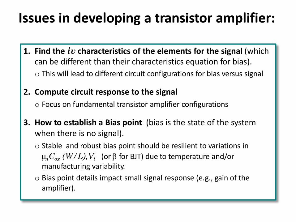
Issues in developing a transistor amplifier:
1. Find the iv characteristics of the elements for the signal (which can be different than their characteristics equation for bias).o This will lead to different circuit configurations for bias versus signal
2. Compute circuit response to the signalo Focus on fundamental transistor amplifier configurations
3. How to establish a Bias point (bias is the state of the system when there is no signal).o Stable and robust bias point should be resilient to variations inµnCox (W/L),Vt (or β for BJT) due to temperature and/ormanufacturing variability.
o Bias point details impact small signal response (e.g., gain of the amplifier).
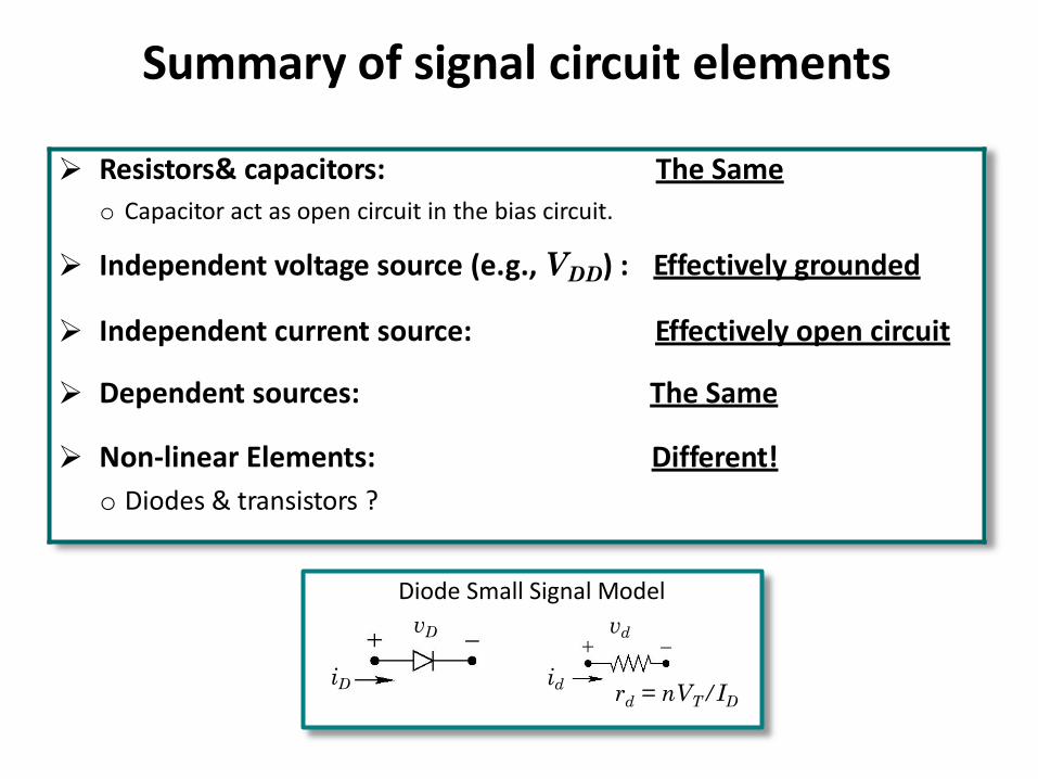
Summary of signal circuit elements
id r = nV /Id T D
Diode Small Signal ModelvD vd
iD
Resistors& capacitors:o Capacitor act as open circuit in the bias circuit.
The Same
Independent voltage source (e.g., VDD) : Effectively grounded
Independent current source: Effectively open circuit
Dependent sources: The Same
Non-linear Elements:o Diodes & transistors ?
Different!

Transistor Small Signal Models
1= 2 ⋅ I D
D
ro ≈OV
m λ ⋅ IVg
Comparison of MOS and BJT small-signal circuit models:1. MOS has an infinite resistor in the input (vgs) while BJT has a finite resistor, rπ
(typically several kΩ).2. BJT gm is substantially larger than that of a MOS (BJT has a much higher gain).3. ro values are typically similar (10s of kΩ). gm ro >> 1 for both.
NMOS/PMOS
C
r ≈ VAo
T π
g = IC = βm
B
= VT
IV rIrπ
NPN/PNP BJT
VT = 26 mV at room temperature

Transistor Biasing To make bias point independent of changes in transistor
parameters (e.g. β,) the bias circuit should “set” IC and NOT IB !
Emitter Degeneration (BJT):
Requires a resistor in the emitter circuit. Requirements:
1. RB << (βmin +1)RE
2. IERE ≥1V
Source Degeneration (MOS):
Requires a resistor in the source circuit. Requirement:
1. RSID >VGS
Current source:

Emitter-degeneration bias circuits
Basic Arrangement Bias with one power supply(voltage divider)
Bias with two power supplies
MOS source-degeneration bias circuits are identical To solve circuits with voltage divider bias:
1. BJT: replace voltage divider with its Thevenin equivalent.2. MOS: Since iG = 0, calculate VG directly.
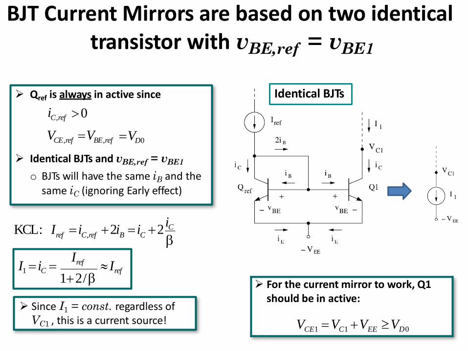
BJT Current Mirrors are based on two identicaltransistor with vBE,ref = vBE1
Identical BJTs Qref is always in active since
Identical BJTs and vBE,ref = vBE1
o BJTs will have the same iB and thesame iC (ignoring Early effect)
=VD0VCE,ref =VBE,ref
iC,ref >0
β+2i = i +2 iC
B CC,refrefKCL: I = i
I1 = iC = ≈Iref1+2/β
Iref
Since I1 = const. regardless ofVC1 , this is a current source!
For the current mirror to work, Q1 should be in active:
VCE1 =VC1 +VEE ≥VD0

MOS Current-Steering Circuit are based on twoidentical transistor with vov,ref = vov1
Qref is always in saturation since
VDS,ref =VGS,ref >VGS,ref
VGS,ref =VGS1 =VGS
VOV ,ref =VOV1 =VOV
−Vt
I = i =0.5µC (W / L) V 21 D1 n ox 1 OV
V 2Iref = iD,ref (W / L)=0.5µC ref OVn ox
I1 = (W / L)1(W / L)refIref
Identical MOS: Same µCox and Vt
Since I = const. regardless of1VD1 , this is a current source!
For the current steering circuit to work, Q1 should be in saturation:
VDS1 >VOV =VGS −Vt

How to add signal to the bias
Bias & SignalvGS = VGS + vgs
Bias & SignalvDS = VDS + vds
1. Direct Coupling Use bias with 2 voltage supplies
o For the first stage, bias such thatVGS = 0
o For follow-up stages, match biasvoltages between stages
Difficult biasing problem Used in ICs Amplifies “DC” signals!
2. Capacitive Coupling Use a capacitor to separate bias
voltage from the signal. Simplified biasing problem. Used in discrete circuits Only amplifies “AC” signals

Discrete CE and CS Amplifiers
Ri = RG
Ro = RD || ro
= −gm (ro || RD || RL )vo
vi
vi
Ri × vo
vsig Ri+Rsig
vo =
Ri = RB || rπRo = RC || ro
rπ →∞
= −gm (ro || RC || RL )vo
vi
BJT
MOS
vi at base, vo at collector

Discrete CE and CS Amplifiers with RE / RS
Ri = RG
Ro = RD ||[ro (1+gmRS )]
vo
vi 1+ gmRS+ (RD || RL ) / ro
gm (RD || RL )= −
rπ + RE + RB || Rsig
Ro = RC || ro1+
1+ [(RC || RL ) / ro ]
R = R || r + R +
vo
vi 1+ gmRE+[(RC || RL ) / ro ](1+ RE / rπ )= −
E
Ei B π E
gm (RC || RL )
βR
βR
vo Ri × vo=vsig Ri+Rsig vi
BJT
MOS
vi at base, vo at collector

Discrete CB and CG Amplifiers
R = R ||r [1+g (r || R || R )]1+ gmro
ro + (RC || RL )Ri = RE || rπ ||
= +gm (ro || RC || RL )
sigEo C o m π
vo
vi
R = R ||r [1+g (R || R )]1+ gmro
r + (R || R )|| o D L
= +gm (ro || RD || RL )
m S sigo D o
S i
vo
vi
R = R
rπ →∞
vo Ri × vo=vsig Ri+Rsig
vi
BJT
MOS
vi at emitter, vo at collector

Discrete CC and CD Amplifiers
R = R || 1
vi 1+ gm (ro || RS || RL )Ri = RG
vo gm (ro || RS || RL )
gmo S
=
vi 1+ gm (ro || RE || RL )Ri = RB ||[rπ + β(ro || RE || RL )]
|| rorπ + RB || RsigRo ≈ RE ||
vo gm (ro || RE || RL )
β
=
vo Ri × vo=vsig Ri+Rsig vi
BJT
MOS
vi at base, vo at emitter

Gain of a multi-stage amplifierExample: A 3-stage amplifier
vi,1 vo,1 vo,2
v v v v= o,3 = o,1 × o,2 × o,3
vi,1 vi,1
vo
× A × ...v3× Av1× Av2v R +R=
sigsig i
Rivo
But we need to know RL,1, RL,2, RL,3, … in order to find AM s.
vo,1 = vi,2 vo,2 = vi,3 vo = vo,3i i,1i,1 sig
Ri,1v
= i,1 , R =Rsigsig
vi
R +Rvv=
Ro = Ro,3
= A × Av2 × Av3v1i,3
o,1 × o,2 × o,3
i,2i,1i,1
o =v v
vv vv vv
vo1 = vi2 vo2 = vi3

What are RL and Rsig for each stage?
Amp Model for Stage j-1
Rsig , j = Ro, j−1
RL, j = Ri, j+1
RL for each stage is the input resistance of the following stage. Rsig for each stage is the output resistance of the previous stage.
Amp Model for Stage j+1

Procedure for Solving multi-stage Amplifiers
Gain & Ri:
1. Start from the load side (nth stage),o Find the gain Av,n = (vo/vi)n and Ri,n .
2. For (n-1)th stage, set RL,n-1 = Ri,n
o Find the gain Av,n-1 = (vo/vi)n-1 and Ri ,n-1 .
3. Repeat until reaching to the first stage. Then,
Ro:
1. Start from the source side (1st stage). Find Ro,1 .
2. Go to the second stage. Set Rsig,2 = Ro,1 . Find Ro,2
3. Continue to the last stage (nth stage). Then, Ro = Ro,n
× Av1× Av2 × Av3
× ...Ri=Ri,1 =
v R +Rsigi
vo Ri
sig

Cut-off frequency of a capacitively coupledamplifier Similar to a single-stage amplifier, each
capacitor introduces a pole:
1) Coupling capacitor at the input:
2) Coupling capacitor at the output:
3) Coupling capacitor between stages j-1 and j
4) By-pass capacitors for stage j (if exists)
5) Then:
i sig c1
f p1 =2π (R +R )C
1
by− pass by− pass
f p ,bypass =2π R C
1
o L co
f po =2π (R +R )C
1
i, j o, j−1 cj
f pj =2π (R +R )C
1
f p ≈ f p1 + f p2 + ...
Diode Functional Circuits

Rectifier & Clipper Circuits
Half-wave rectifier
(Diode ON)(Diode OFF)
For vi ≥ VD0 , vo = vi −VD0
For vi <VD0 , vo = 0
Clipper
(Diode ON)(Diode OFF)
For vi ≥ VD0 , vo =VD0
For vi <VD0 , vo = vi

“Clipping” voltage can be adjustedvo limited to ≤ VD0 + VDC vo limited to ≤ VD0 + VZ
vo limited to ≥ − VD0 − VDC vo limited ≥ − VD0 −VZ

Both top & bottom portions of the signal can be clipped simultaneously
vo limited to ≤ VD0 + VDC1 and ≥ − VD0 − VDC2
vo limited to ≤ VD0 + VZ1and ≥ − VD0 − VZ2

Clamp Circuit
Peak Detector & Clamp Circuits
“ideal” peak detector: τ/T → ∞
“Good” peak detector: τ/T >> 1
vo is equal to vi but shifted “downward” by − (V + − VD0)
Peak Detector Circuit

vo shifted “downward”
Voltage shift in a clamp circuit can be adjusted!
−VZ −VD0 )vo = vi − (V +vo = vi − (V −VDC −VD0 )+
vo shifted “upward”
vo = vi + (V −VZ −VD0 )−vo = vi + (V −VDC −VD0 )−

BJT as a switch
Use: Logic gate can turn loads ON (BJT in saturation) or OFF (BJT in cut-off)
ic is uniquely set by CE circuit (as vce = Vsat)
RB is chosen such that BJT is in deep saturation with a wide margin (e.g., iB = 0.2 ic /β)
*Lab 4 circuit
Load is placed in collector circuit
Solved in Lecture notes (problems 12 & 13)
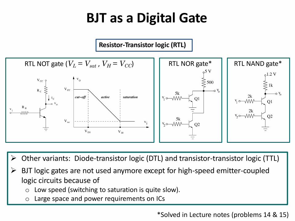
BJT as a Digital Gate
Other variants: Diode-transistor logic (DTL) and transistor-transistor logic (TTL) BJT logic gates are not used anymore except for high-speed emitter-coupled
logic circuits because ofo Low speed (switching to saturation is quite slow).o Large space and power requirements on ICs
RTL NOT gate (VL = Vsat , VH = VCC)
Resistor-Transistor logic (RTL)
RTL NOR gate* RTL NAND gate*
*Solved in Lecture notes (problems 14 & 15)

NMOS Functional circuits
Similar to a BJTs in the active mode,NMOS behaves rather “linearly” in the saturation region
Transition from cut-off to triode can be used to build NMOS switch circuits.o Voltage at point C (see graph)
depends on NMOS parameters and the circuit (in BJT vo = Vsat)!
We can also built NMOS logic gatesimilar to a RTL. But there is are much better gates based on CMOS technology!
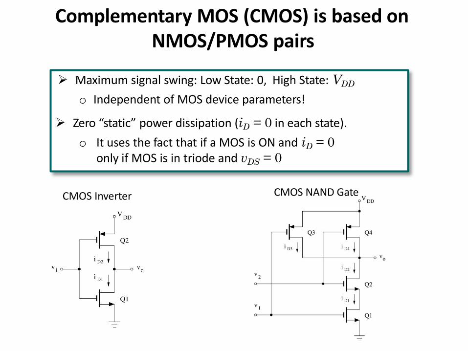
Complementary MOS (CMOS) is based onNMOS/PMOS pairs
Maximum signal swing: Low State: 0, High State: VDD
o Independent of MOS device parameters!
Zero “static” power dissipation (iD = 0 in each state).o It uses the fact that if a MOS is ON and iD = 0
only if MOS is in triode and vDS = 0
CMOS Inverter CMOS NAND Gate

How to Solve Problems
1. What is Known? (comes from problem description.)
2. What is the aim? (Identify circuit parameters that haveto be calculated.)3. How to get there?
(use recipes!)
First, write down all equations that govern thecircuit.
Make sure that you have enough equations to solve for the unknowns.
Make sure that your solutions will give you theanswer to the problem.
Only then, start solving the equations.