lecture 13: interconnects in cmos...
TRANSCRIPT

VLSI-1 Class Notes
Lecture 13:Interconnects in CMOS Technology
Mark McDermottElectrical and Computer Engineering
The University of Texas at Austin
10/18/18
VLSI-1 Class Notes
Introduction
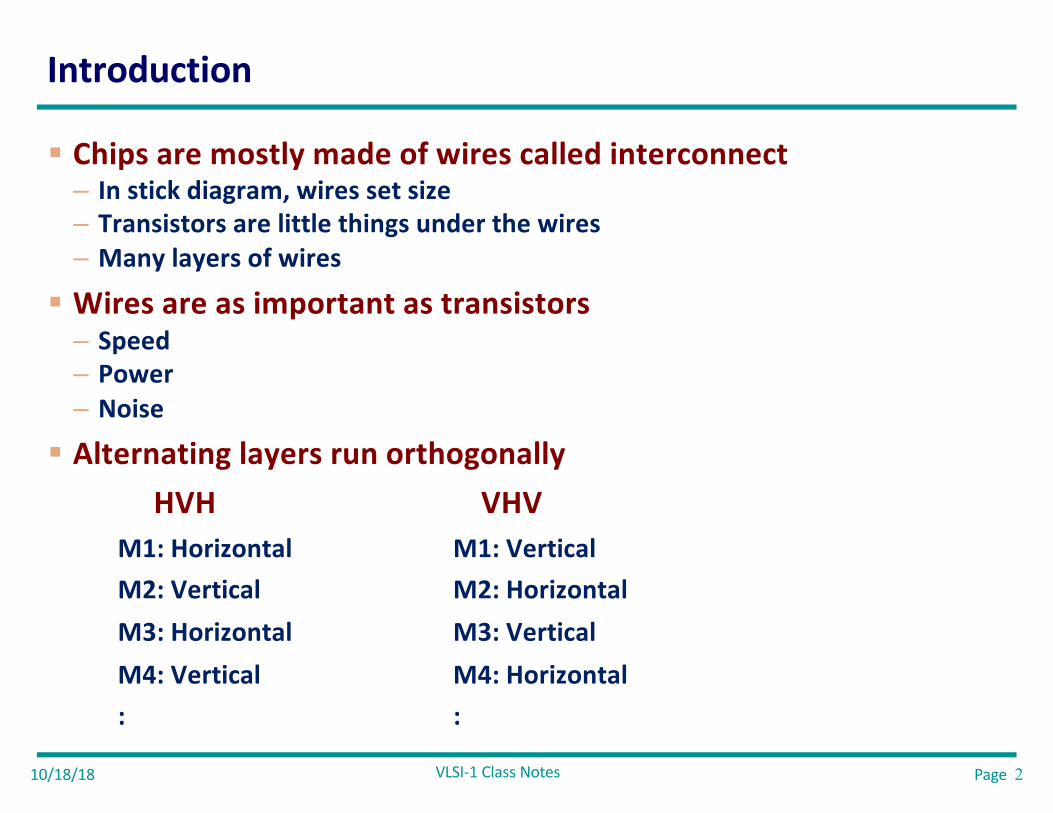
§ Chips are mostly made of wires called interconnect– In stick diagram, wires set size– Transistors are little things under the wires– Many layers of wires
§ Wires are as important as transistors– Speed– Power– Noise
§ Alternating layers run orthogonallyHVH VHV
M1: Horizontal M1: VerticalM2: Vertical M2: HorizontalM3: Horizontal M3: VerticalM4: Vertical M4: Horizontal: :
10/18/18 Page 2
VLSI-1 Class Notes
Choice of Metals
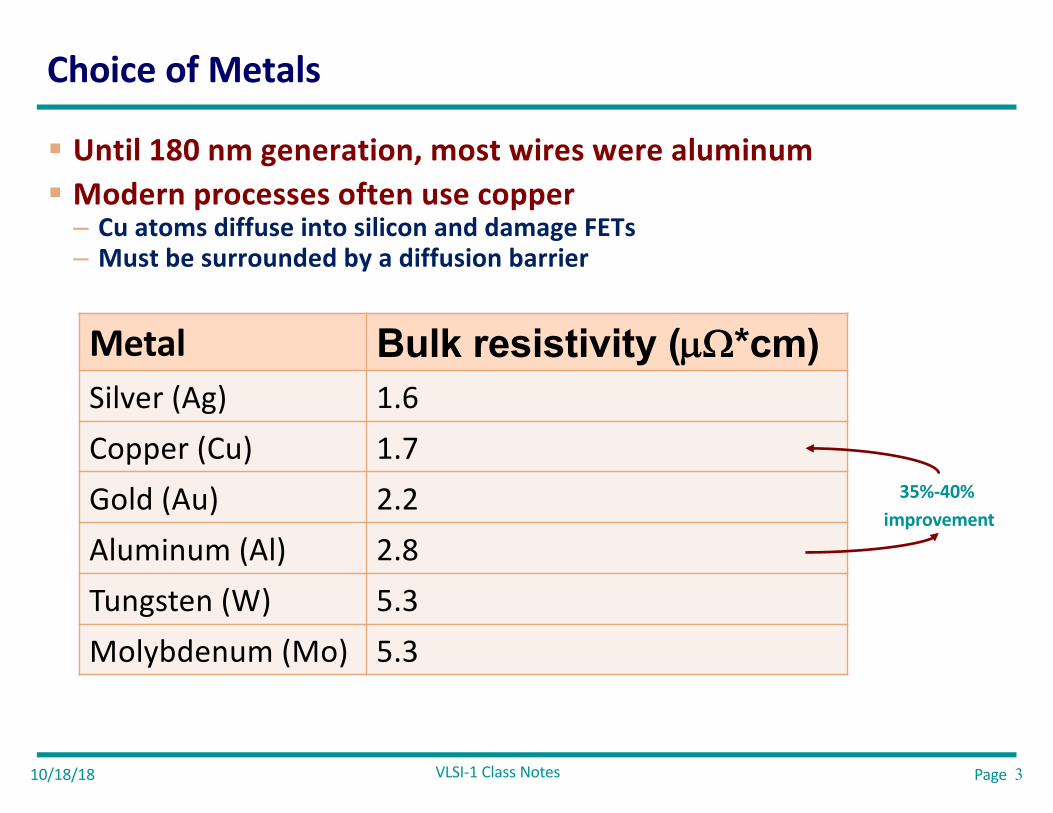
§ Until 180 nm generation, most wires were aluminum§ Modern processes often use copper– Cu atoms diffuse into silicon and damage FETs– Must be surrounded by a diffusion barrier
Metal Bulk resistivity (µµWW*cm)Silver (Ag) 1.6Copper (Cu) 1.7Gold (Au) 2.2Aluminum (Al) 2.8Tungsten (W) 5.3Molybdenum (Mo) 5.3
10/18/18 Page 3
35%-40% improvement

VLSI-1 Class Notes
Metal Layer Cross Section 65nM
200nM
180nM
100nM 100nM 90nM
110nM
Barrier Metal
<6nM
10/18/18 Page 4

VLSI-1 Class Notes
Loose pitch + thick metal on upper layers:High speed global wiresLow resistance power grid
Tight pitch on lower layers:Maximum density for local interconnects
Source: Mark Bohr, Intel Corporation
45nm Interconnect
410/18/18 Page 5

VLSI-1 Class Notes •6
METAL 2
METAL 1METAL 1
W VIA
POLYCIDE
W CONTACT
Courtesy: IBM
SEM MICRO-GRAPH (ILM DIELECTRIC REMOVED)
510/18/18

VLSI-1 Class Notes
Advanced Metallization
© Digital Integrated Circuits2nd
10/18/18 Page 7

VLSI-1 Class Notes
Interconnect Process Dual Damascene
Page 8
•C.-K. Hu and J.M.E. Harper, Mater. Chem. Phys., 52 (1998), p. 5.
10/18/18

VLSI-1 Class Notes
R=rL/twl
w s
t
h
L
7
WIRE GEOMETRY
§ PITCH = width + space
§ Height (h) = distance to top/bottom routes
§ ASPECT RATIO (AR) = thickness / width– Deep submicron processes have AR < 2 to maintain sheet resistances at a
reasonable level– Coupling to neighboring routes dominates
10/18/18 Page 9

VLSI-1 Class Notes
Wire Resistance
§ rr = resistivity (WW*m)
§ Roo = sheet resistance (WW/oo)– oo is a dimensionless unit(!)
§ Count number of squares– R = Roo * (# of squares) l
w
t
1 Rectangular BlockR = R (L/W) W
4 Rectangular BlocksR = R (2L/2W) W = R (L/W) W
t
l
w w
l
l lR Rt w wr
= = !
10/18/18 Page 10
where r=resistivity

VLSI-1 Class Notes
Sheet Resistance
§ Typical sheet resistances in 180 nm process
Layer Sheet Resistance (WW/oo)Diffusion (silicided) 3-10Diffusion (no silicide) 50-200Polysilicon (silicided) 3-10Polysilicon (no silicide) 50-400Metal1 0.08Metal2 0.05Metal3 0.05Metal4 0.03Metal5 0.02Metal6 0.02
10/18/18 Page 11

VLSI-1 Class Notes
CONTRIBUTION OF WIRES (they are not free)
§ DELAY– Function of R, L and C, VIA resistance, local .vs. global
§ POWER– Charging/discharging of C is a function of CV2F
§ NOISE– Attackers/victims impact on functionality and delay
§ POWER SUPPLY IR DROPS and GROUND BOUNCE– Affects delay leading to timing failures
§ RELIABILITY– Electro-migration, self heat, maximum current
§ COST– Number of layers .vs. area/performance targets, yield
10/18/18 Page 12
VLSI-1 Class Notes
Contact/VIA Resistance
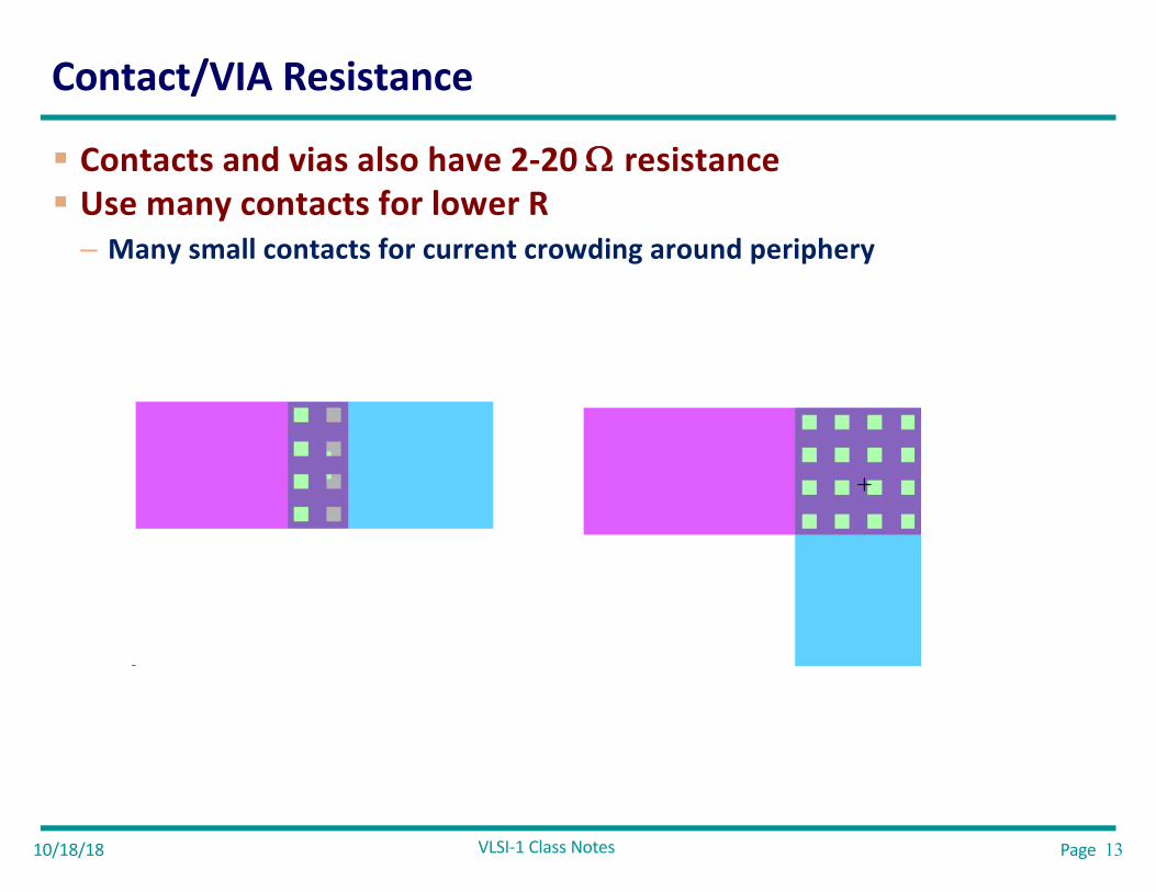
§ Contacts and vias also have 2-20 WW resistance§ Use many contacts for lower R– Many small contacts for current crowding around periphery
10/18/18 Page 13

VLSI-1 Class Notes
Wire Capacitance
§ Wire has capacitance per unit length– To neighbors– To layers above and below
§ Ctotal = Ctop + Cbot + 2Cadj
layer n+1
layer n
layer n-1
Cadj
Ctop
Cbot
ws
t
h1
h2
10/18/18 Page 14

VLSI-1 Class Notes
Capacitance Trends
§ Parallel plate equation: C = eeA/d–Wires are not parallel plates, but obey trends
– Increasing area (W, t) increases capacitance
– Increasing distance (s, h) decreases capacitance
§Dielectric constant– ee = kee0
§ ee0 = 8.85 x 10⁻¹⁴ F/cm§ k = 3.9 for SiO2
§ Processes are starting to use low-k dielectrics– k »» 3 (or less) as dielectrics use air pockets
10/18/18 Page 15

VLSI-1 Class Notes
M2 Capacitance Data
§ Typical wires have ~ 0.2 fF/µµm– Compare to 2 fF/µµm for gate
capacitance
0
50
100
150
200
250
300
350
400
0 500 1000 1500 2000
Cto
tal (
aF/µ
m)
w (nm)
Isolated
M1, M3 planes
s = 320s = 480s = 640s= 8
s = 320s = 480s = 640s= 8
10/18/18 Page 16
VLSI-1 Class Notes
Diffusion & Polysilicon
§ Diffusion capacitance is very high (about 2 fF/µµm)– Comparable to gate capacitance– Diffusion also has high resistance– Avoid using diffusion runners for wires!
§ Polysilicon has lower C but high R– Use for transistor gates– Occasionally for very short wires between gates
10/18/18 Page 17
VLSI-1 Class Notes
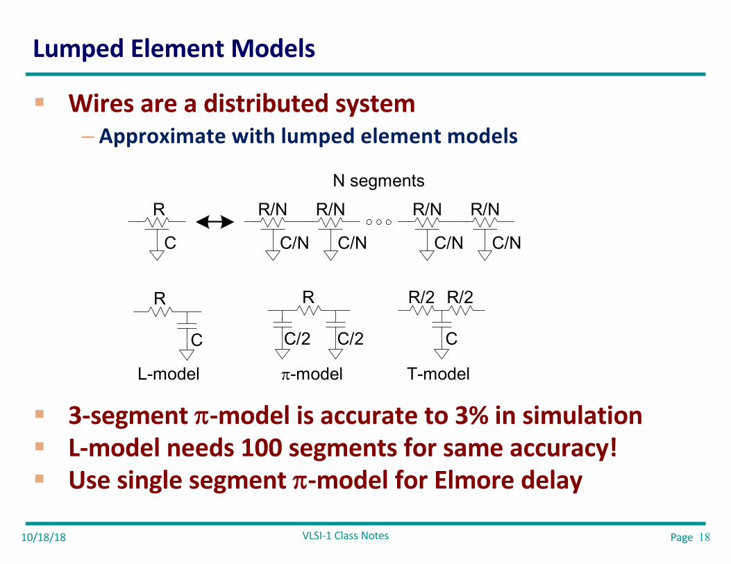
Lumped Element Models
§ Wires are a distributed system– Approximate with lumped element models
§ 3-segment pp-model is accurate to 3% in simulation§ L-model needs 100 segments for same accuracy!§ Use single segment pp-model for Elmore delay
C
R
C/N
R/N
C/N
R/N
C/N
R/N
C/N
R/N
R
C
L-model
R
C/2 C/2
R/2 R/2
C
N segments
p-model T-model
10/18/18 Page 18

VLSI-1 Class Notes
Example
§ Metal2 wire in 180 nm process– 5 mm long– 0.32 µµm wide
§ Construct a 3-segment pp-model– Roo = 0.05 WW/oo => R = 781 WW– Cpermicron = 0.2 fF/µµm => C = 1 pF
260 W
167 fF 167 fF
260 W
167 fF 167 fF
260 W
167 fF 167 fF
10/18/18 Page 19

VLSI-1 Class Notes
Wire RC Delay
§ Estimate the delay of a 10x inverter driving a 2x inverter at the end of the 5mm wire from the previous example.– R = 2.5 kWW*µµm for gates– Unit inverter: 0.36 µµm nMOS, 0.72 µµm pMOS
– tpd = 1.1 ns 781 W
500 fF 500 fF
Driver Wire
4 fF
Load
690 W
10/18/18 Page 20

VLSI-1 Class Notes
Crosstalk
§ A capacitor does not like to change its voltage instantaneously.
§ A wire has high capacitance to its neighbor.– When the neighbor switches from 1-> 0 or 0->1, the wire tends to switch too.– Called capacitive coupling or crosstalk.
§ Crosstalk effects– Noise on non-switching wires– Increased delay on switching wires
10/18/18 Page 21

VLSI-1 Class Notes
Crosstalk Delay
§ Assume layers above and below on average are quiet– Second terminal of capacitor can be ignored– Model as Cgnd = Ctop + Cbot
§ Effective Cadj depends on behavior of neighbors– Miller Coupling Factor (MCF)
A BCadjCgnd Cgnd
B DV Ceff(A) MCFConstant VDD Cgnd + Cadj 1Switching with A 0 Cgnd 0Switching opposite A 2VDD Cgnd + 2 Cadj 2
10/18/18 Page 22
VLSI-1 Class Notes
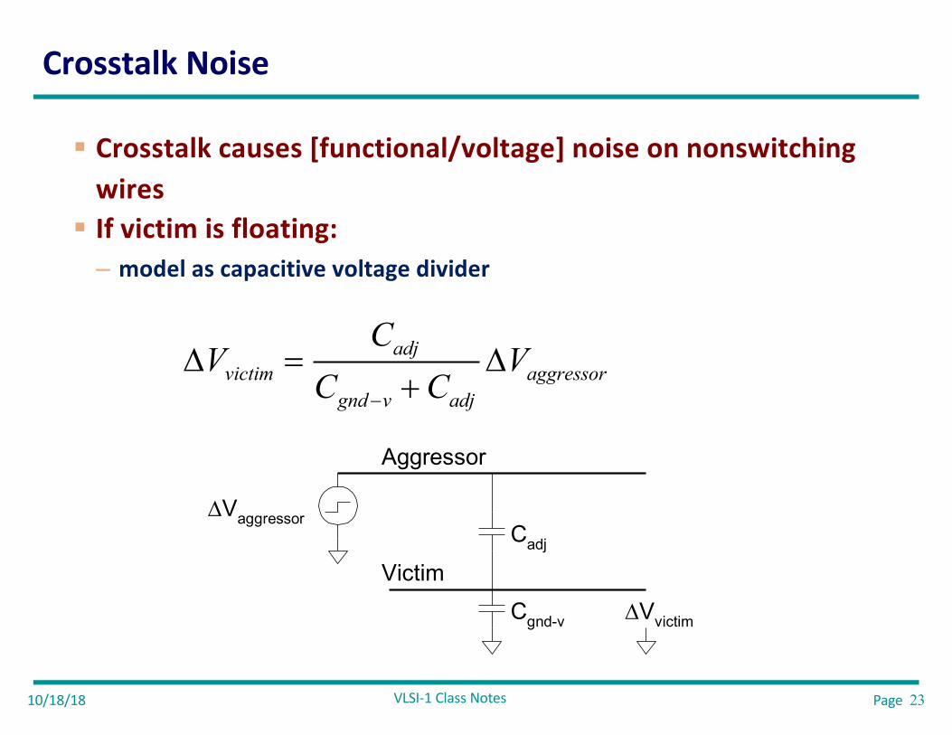
Crosstalk Noise
§ Crosstalk causes [functional/voltage] noise on nonswitchingwires
§ If victim is floating:– model as capacitive voltage divider
Cadj
Cgnd-v
Aggressor
Victim
DVaggressor
DVvictim
adjvictim aggressor
gnd v adj
CV V
C C-
D = D+
10/18/18 Page 23

VLSI-1 Class Notes
Driven Victims
§ Usually victim is driven by a gate that fights noise– Noise depends on relative resistances– Victim driver is in linear region, aggressor in saturation– If sizes are same, Raggressor = 2-4 x Rvictim
11
adjvictim aggressor
gnd v adj
CV V
C C k-
D = D+ +
( )( )
aggressor gnd a adjaggressor
victim victim gnd v adj
R C Ck
R C Ctt
-
-
+= =
+
Cadj
Cgnd-v
Aggressor
Victim
DVaggressor
DVvictim
Raggressor
Rvictim
Cgnd-a
10/18/18 Page 24

VLSI-1 Class Notes
Coupling Waveforms
§ Simulated coupling for Cadj = Cvictim
Aggressor
Victim (undriven): 50%
Victim (half size driver): 16%
Victim (equal size driver): 8%Victim (double size driver): 4%
t (ps)0 200 400 600 800 1000 1200 1400 1800 2000
0
0.3
0.6
0.9
1.2
1.5
1.8
10/18/18 Page 25

VLSI-1 Class Notes
Noise Implications
§ Do we care if we have noise?
§ If the noise is less than the noise margin, nothing happens
§ Static CMOS logic will eventually settle to correct output even if disturbed by large noise spikes– But glitches cause extra delay– Also cause extra power from false transitions
§ Dynamic logic never recovers from glitches
§ Memories and other sensitive circuits also can produce the wrong answer
Page 2610/18/18
VLSI-1 Class Notes
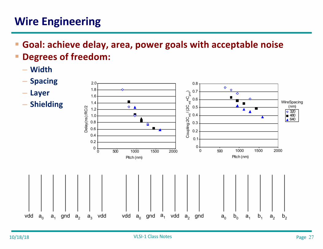
Wire Engineering
§ Goal: achieve delay, area, power goals with acceptable noise§ Degrees of freedom:– Width – Spacing– Layer– Shielding
Del
ay (n
s): R
C/2
Wire Spacing(nm)
Cou
plin
g: 2C
adj /
(2C
adj+C
gnd)
00.20.40.6
0.81.01.21.4
1.61.82.0
0 500 1000 1500 20000
0.1
0.2
0.3
0.4
0.5
0.6
0.7
0.8
0 500 1000 1500 2000
320480640
Pitch (nm)Pitch (nm)
vdd a0 a1gnd a2vdd b0 a1 a2 b2vdd a0 a1 gnd a2 a3 vdd gnd a0 b1
10/18/18 Page 27
VLSI-1 Class Notes
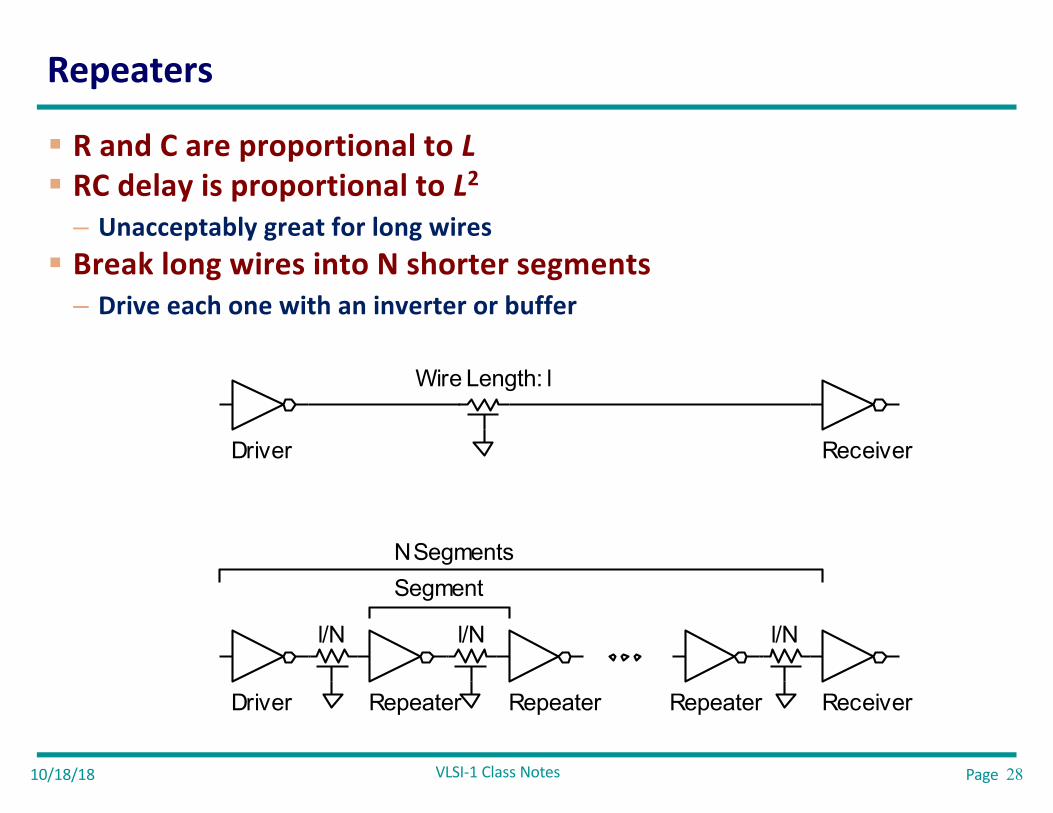
Repeaters
§ R and C are proportional to L§ RC delay is proportional to L2
– Unacceptably great for long wires§ Break long wires into N shorter segments– Drive each one with an inverter or buffer
Wire Length: l
Driver Receiver
l/N
Driver
Segment
Repeater
l/N
Repeater
l/N
ReceiverRepeater
N Segments
10/18/18 Page 28

VLSI-1 Class Notes
0
100
200
300
400
500
600
700
0 500 1000 1500 2000 2500 3000 3500
M3
M4
M5
M6
Pico
seco
nds
130 nm Copper
Repeated Interconnect
10/18/18 Page 29

VLSI-1 Class Notes
Repeater Design
§ How many repeaters should we use?
§ How large should each one be?
§ Equivalent Circuit– Wire length l
• Wire Capacitance CCww**ll & Resistance RRww**ll– Inverter width W (nMOS = W, pMOS = 2W)
• Gate Capacitance CC **WW & Resistance RR//WW
R/W C'WCwl/2N Cwl/2N
RwlN
10/18/18 Page 30
VLSI-1 Class Notes
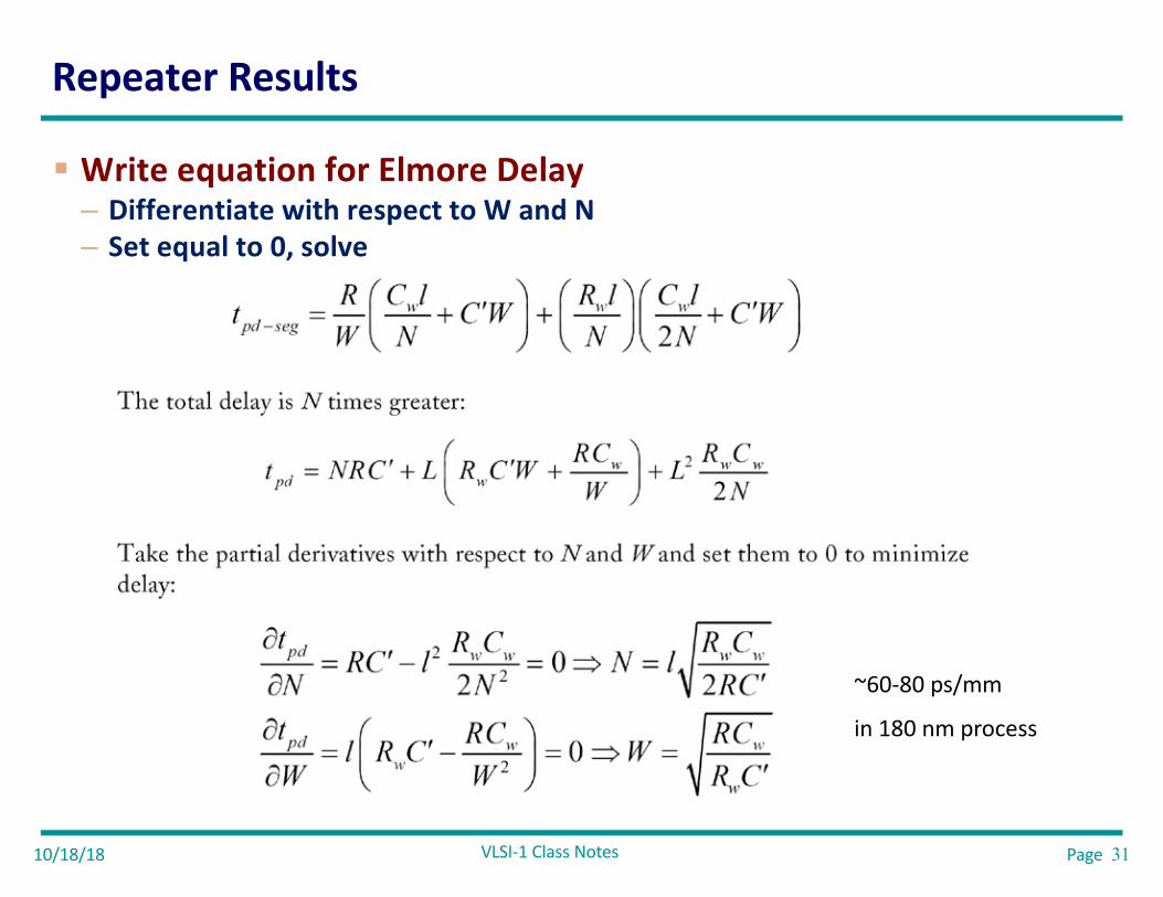
Repeater Results
§ Write equation for Elmore Delay– Differentiate with respect to W and N– Set equal to 0, solve
~60-80 ps/mm
in 180 nm process
10/18/18 Page 31

VLSI-1 Class Notes
Staggering the inverters
Avoiding the Miller cap by opposite going signals
Repeater Placements
10/18/18 Page 32

VLSI-1 Class Notes
BACKUP
10/18/18 Page 33

VLSI-1 Class Notes
Layer Stack
§ AMI 0.6 µµm process has 3 metal layers§ Modern processes use 6-10+ metal layers§ Example:
Intel 180 nm process§ M1: thin, narrow (< 3ll)– High density cells
§ M2-M4: thicker– For longer wires
§ M5-M6: thickest– For VDD, GND, clk
Layer T (nm) W (nm) S (nm) AR
6 1720 860 860 2.0
1000
5 1600 800 800 2.0
1000
4 1080 540 540 2.0
7003 700 320 320 2.2
7002 700 320 320 2.2
7001 480 250 250 1.9
800
Substrate
10/18/18 Page 34