lecture 07: risc-v single-cycle implementation · –slides for general risc isa implementation are...
TRANSCRIPT

Lecture07:RISC-VSingle-CycleImplementation
CSCE513ComputerArchitecture
DepartmentofComputerScienceandEngineeringYonghong Yan
[email protected]://passlab.github.io/CSCE513
1

Acknowledgements
• ThenotescoverAppendixCofthetextbook– SlidesforgeneralRISCISAimplementationareadaptedfrom
Lectureslidesfor“ComputerOrganizationandDesign,RISC-VEdition:TheHardware/SoftwareInterface”textbookforgeneralRISCISAimplementation
– SlidesforRISC-Vsingle-cycleimplementationareadaptedfromComputerScience152:ComputerArchitectureandEngineering,Spring2016byDr.GeorgeMichelogiannakis fromUCBerkeley
2
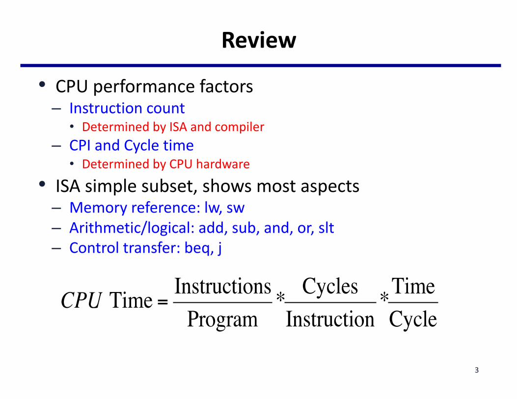
Review
• CPUperformancefactors– Instructioncount
• DeterminedbyISAandcompiler– CPIandCycletime
• DeterminedbyCPUhardware
• ISAsimplesubset,showsmostaspects– Memoryreference:lw,sw– Arithmetic/logical:add,sub,and,or,slt– Controltransfer:beq,j
CPU Time = InstructionsProgram
* CyclesInstruction
*TimeCycle
3
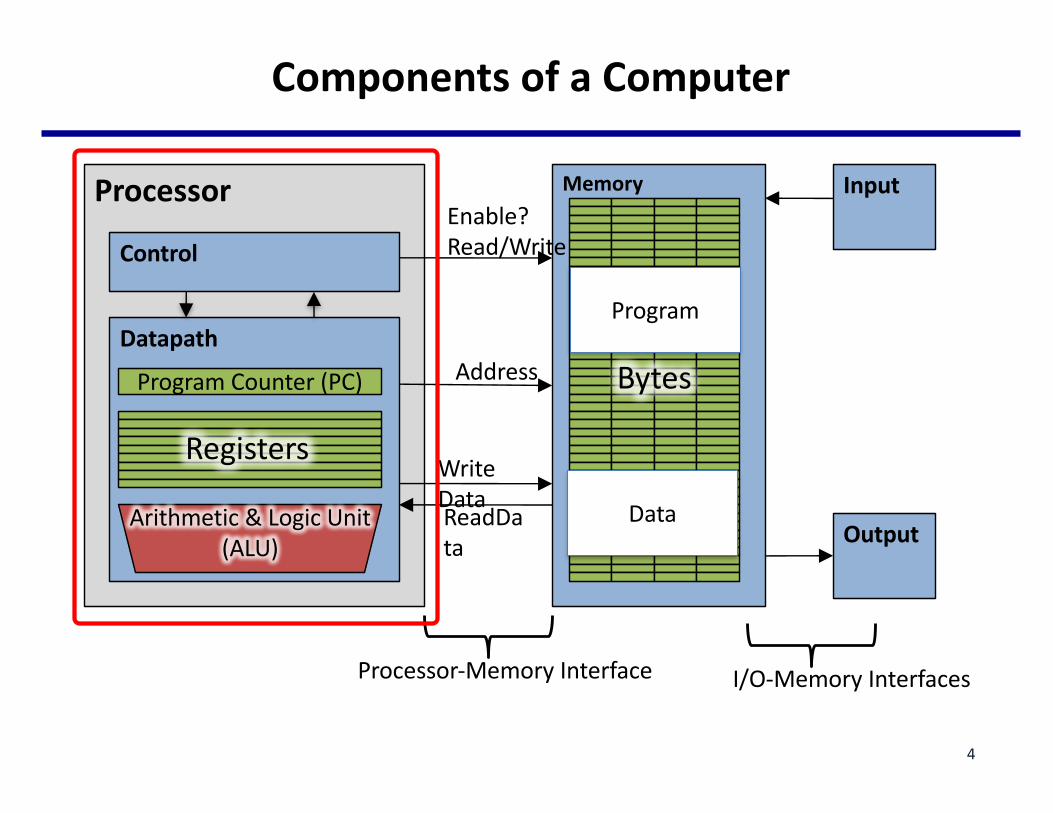
Processor
Control
Datapath
ComponentsofaComputer
ProgramCounter(PC)
Registers
Arithmetic&LogicUnit(ALU)
Memory Input
Output
Bytes
Enable?Read/Write
Address
WriteDataReadData
Processor-MemoryInterface I/O-MemoryInterfaces
Program
Data
4

Datapath andControl
• Datapath designedtosupportdatatransfersrequiredbyinstructions
• Controllercausescorrecttransferstohappen
5
Controlleropcode, funct
inst
ruct
ion
mem
ory
+4
rtrsrd
regi
ster
sALU
Dat
am
emor
y
imm
PC
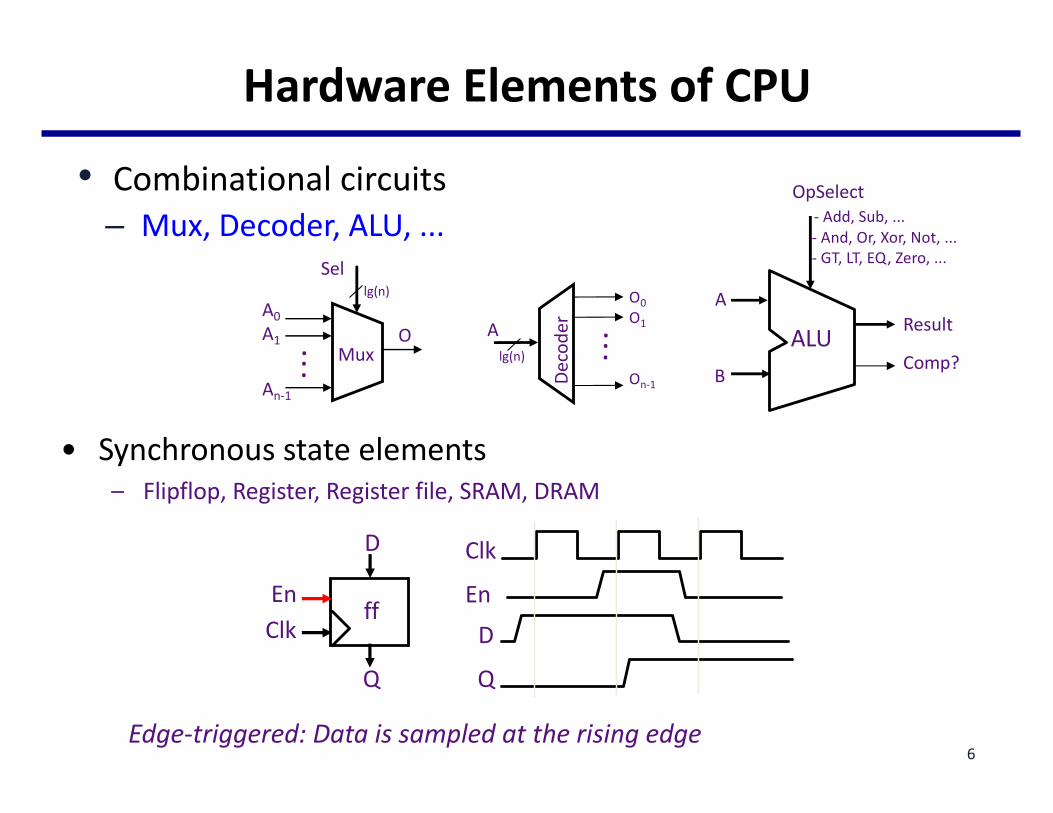
HardwareElementsofCPU
• Combinationalcircuits– Mux,Decoder,ALU,...
• Synchronousstateelements– Flipflop,Register,Registerfile,SRAM,DRAM
Edge-triggered:Dataissampledattherisingedge
Clk
D
Q
Enff
Q
D
ClkEn
OpSelect- Add,Sub,...- And,Or,Xor,Not,...- GT,LT,EQ,Zero,...
Result
Comp?
A
B
ALU
Sel
OA0A1
An-1
Mux...
lg(n)
A
Decode
r ...
O0O1
On-1
lg(n)
6

RegisterFiles
• Readsarecombinational– Canreadinanycycleandformultiplereads– Only2registersourceoperandsneeded
7
ReadData1ReadSel1ReadSel2
WriteSel
Registerfile
2R+1W
ReadData2
WriteData
WEClock
rd1rs1
rs2
ws
wd
rd2
we
ff
Q0
D0
ClkEn
ff
Q1
D1
ff
Q2
D2
ff
Qn-1
Dn-1
...
...
...
register

RegisterFileImplementation
• RISC-Vintegerinstructionshaveatmost2registersourceoperands
8
reg31
rd clk
reg1
wdata
we
rs1rdata1 rdata2
reg0
…
32
…
5 32 32
…
rs255

ASimpleMemoryModel
• Readsandwritesarealwayscompletedinonecycle• Readcanbedoneanytime(i.e.combinational)• Writeisperformedattherisingclockedge
– ifitisenabled
9
RAM ReadData
WriteData
Address
WriteEnableClock

FiveStagesofInstructionExecution
• Stage1:InstructionFetch
• Stage2:InstructionDecode
• Stage3:ALU(Arithmetic-LogicUnit)
• Stage4:MemoryAccess
• Stage5:RegisterWrite
10
Reg ALU DMemIfetch Reg
IF ID/RF EX MEM WB

StagesofExecutionandDatapath
inst
ruct
ion
mem
ory
+4
rtrsrd
regi
ster
s
ALU
Dat
am
emor
y
imm
1.InstructionFetch
2.Decode/RegisterRead
3.Execute 4.Memory 5.RegisterWrite
PC
11

StagesofExecution(1/5)
• Awidevarietyofinstructions:sowhatgeneralstepsdotheyhaveincommon?– Focus:
• Memoryreference:lw,sw• Arithmetic/logical:add,sub,and,or,slt• Controltransfer:beq,j
• Stage1:InstructionFetch– The32-bitinstructionwordmustfirstbefetchedfrommemory
• Thecache-memoryhierarchy– IncrementPC
• PC=PC+4,topointtothenextinstruction– byteaddressingso+4
12
Reg ALU DMemIfetch Reg
IF ID/RF EX MEM WB
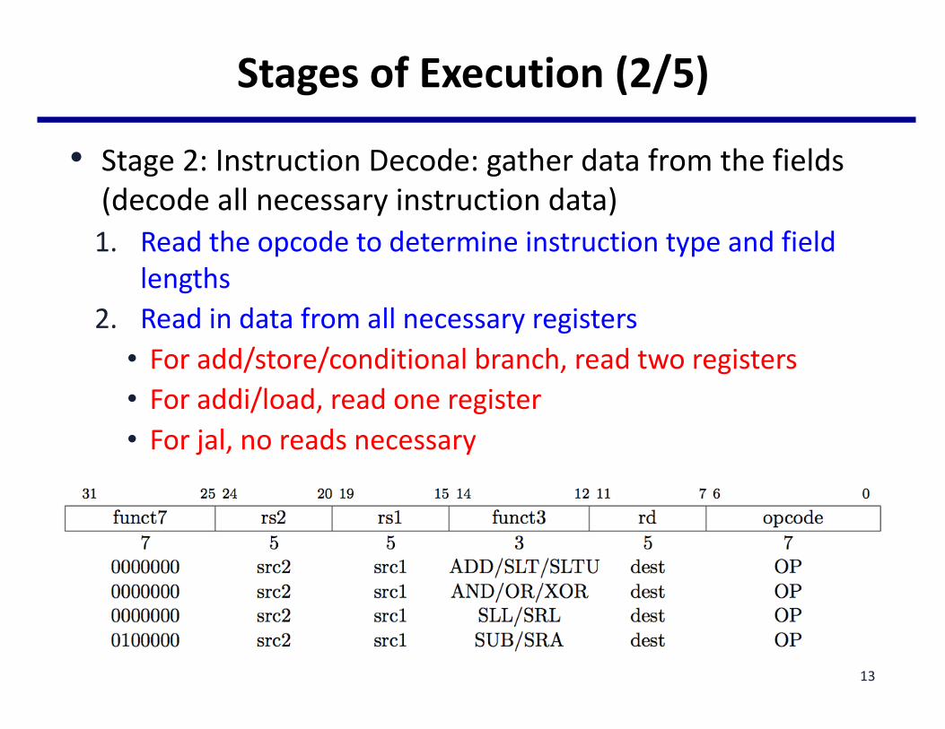
StagesofExecution(2/5)
• Stage2:InstructionDecode:gatherdatafromthefields(decodeallnecessaryinstructiondata)1. Readtheopcode todetermineinstructiontypeandfield
lengths2. Readindatafromallnecessaryregisters
• Foradd/store/conditionalbranch,readtworegisters• Foraddi/load,readoneregister• Forjal,noreadsnecessary
13

StagesofExecution(3/5)
• Stage3:ALU(Arithmetic-LogicUnit):therealworkofmostinstructionsisdonehere– ALoperations:
• arithmetic(+,-,*,/),shifting,logic(&,|),comparisons(slt)– Loadsandstores:additionisdone
• lw $R4,40($R1)• Addtocalcuate thetheaddressforaccessingmemory
– [$R4]+40– Conditionalbranch:comparisonisdoneinthisstage(one
solution)• BEQ$R3,$R4,128
– [$R3]- [$R4]
14

StagesofExecution(4/5)
• Stage4:MemoryAccess:onlyforloadandstore– Theotherinstructionsremainidleduringthisstageorskipit
alltogether– Sinceload/storehaveauniquestep,weneedthisextrastage
toaccountforthem– Asaresultofthecachesystem,thisstageisexpectedtobe
fast• 1cycleideally
15
Reg ALU DMemIfetch Reg
IF ID/RF EX MEM WB

StagesofExecution(5/5)
• Stage5:RegisterWrite– Mostinstructionswritetheresultofsomecomputationintoa
register• Arithmetic,logical,shifts,loads,slt
– Forstores,branches,jumps:• Don’twriteanythingintoaregisterattheend• Theyremainidleduringthisfifthstageorskipitalltogether
16
Reg ALU DMemIfetch Reg
IF ID/RF EX MEM WB

CPUComponentsandMajorDatapath
17
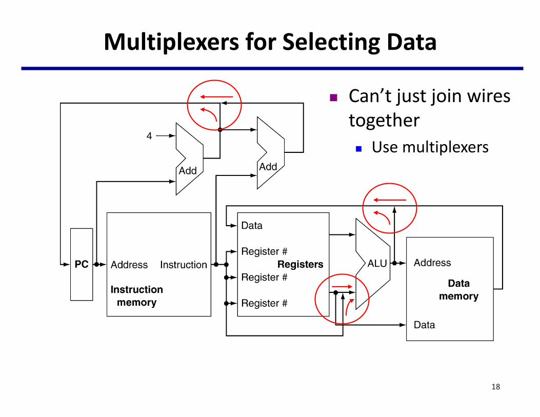
MultiplexersforSelectingData
n Can’tjustjoinwirestogethern Usemultiplexers
18

ControlSignals
• ForselectinginputinMux,andenablingregisterwrite,memoryreadandwrite,andALU
19

BuildingDatapath
• Datapath– ElementsthatprocessdataandaddressesintheCPU
• Registers,ALUs,mux’s,memories,…• TobuildaRISCVdatapath incrementally
– Refiningtheoverviewdesign
20

Datapath forInstructionFetch
32-bitregister
Incrementby4fornextinstruction
21

R-FormatInstructions
• Readtworegisteroperands• Performarithmetic/logicaloperation• Writeregisterresult
22

Load/StoreInstructions
• Readregisteroperands• Calculateaddressusing12-bitoffset
– UseALU,butsign-extendoffset• Load:Readmemoryandupdateregister• Store:Writeregistervaluetomemory
23

Datapath forR|I-Type,LoadandStore
24

BranchInstructions
• Readregisteroperands• Compareoperands:ToTakeorNot
– UseALU,subtractandcheckZerooutput• Calculatetargetaddress:Wherebranchto
– Sign-extenddisplacement– Shiftleft2places(worddisplacement)– AddtoPC+4
• Alreadycalculatedbyinstructionfetch
25

Datapath forBranchInstructions
Justre-routeswires
Sign-bitwirereplicated
26

FullDatapath
27
InMoreDetailsusingRISC-V
28

Datapath:Reg-RegALUInstructions
29
RegWrite Timing?
0x4Add
clk
addrinst
Inst.Memory
PC
Inst<19:15>Inst<24:20>
Inst<11:7>
Inst<14:12>
OpCode
ALU
ALUControl
RegWriteEn
clk
rd1
GPRs
rs1rs2
wawd rd2
we
7 5 5 3 5 7func7 rs2 rs1 func3 rd opcode rd ¬ (rs1) func (rs2)
31 25 24 20 19 15 14 12 11 7 6 0

Datapath:Reg-ImmALUInstructions
30
ImmSelect
ImmSel
Inst<31:20>
OpCode
0x4Add
clk
addrinst
Inst.Memory
PCALU
RegWriteEn
clk
rd1
GPRs
rs1rs2
wawd rd2
weInst<19:15>
Inst<11:7>
Inst<14:12> ALUControl
12 5 3 5 7immediate12 rs1 func3 rd opcode rd ¬ (rs1) op immediate31 20 19 15 14 12 11 7 6 0
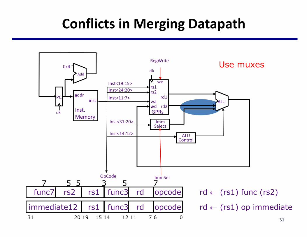
ConflictsinMergingDatapath
31
ImmSelect
ImmSelOpCode
0x4Add
clk
addrinst
Inst.Memory
PCALU
RegWrite
clk
rd1
GPRs
rs1rs2
wawd rd2
weInst<19:15>
Inst<11:7>
Inst<31:20>
Inst<14:12> ALUControl
Use muxes
Inst<24:20>
7 5 5 3 5 7func7 rs2 rs1 func3 rd opcode rd ¬ (rs1) func (rs2)
immediate12 rs1 func3 rd opcode rd ¬ (rs1) op immediate31 20 19 15 14 12 11 7 6 0

Datapath forALUInstructions
32
<14:12>
Op2SelReg /Imm
ImmSelect
ImmSelOpCode
0x4Add
clk
addrinst
Inst.Memory
PCALU
RegWriteEnclk
rd1
GPRs
rs1rs2
wawd rd2
we<19:15><24:20>
ALUControl
<11:7>
<6:0>
7 5 5 3 5 7func7 rs2 rs1 func3 rd opcode rd ¬ (rs1) func (rs2)
immediate12 rs1 func3 rd opcode rd ¬ (rs1) op immediate31 20 19 15 14 12 11 7 6 0
Inst<31:20>

Load/StoreInstructions
33
WBSelALU/Mem
rs1 is the base registerrd is the destination of a Load, rs2 is the data source for a Store
Op2Sel
“base”
disp
ImmSelOpCode
ALUControl
ALU
0x4Add
clk
addrinst
Inst.Memory
PC
RegWriteEn
clk
rd1
GPRs
rs1rs2
wawd rd2
we
ImmSelect
clk
MemWrite
addr
wdata
rdataDataMemory
we
7 5 5 3 5 7imm rs2 rs1 func3 imm opcode Store (rs1) + displacement
immediate12 rs1 func3 rd opcode Load31 20 19 15 14 12 11 7 6 0

RISC-VConditionalBranches
• Comparetwointegerregistersforequality(BEQ/BNE)orsignedmagnitude(BLT/BGE)orunsignedmagnitude(BLTU/BGEU)
• 12-bitimmediateencodesbranchtargetaddressasasignedoffsetfromPC,inunitsof16-bits(i.e.,shiftleftby1thenaddtoPC).
34
7
6 0opcode
5
11 7imm
3
14 12func3
5
19 15rs1
5
24 20rs2
7
31 25imm
BEQ/BNEBLT/BGEBLTU/BGEU

ConditionalBranches(BEQ/BNE/BLT/BGE/BLTU/BGEU)
35
0x4
Add
PCSel
clk
WBSelMemWrite
addr
wdata
rdataDataMemory
we
Op2SelImmSelOpCode
Bcomp?
clk
clk
addrinst
Inst.Memory
PC rd1
GPRs
rs1rs2
wawd rd2
we
ImmSelect
ALU
ALUControl
Add
br
pc+4
RegWrEn
BrLogic
7
6 0opcode
5
11 7imm
3
14 12func3
5
19 15rs1
5
24 20rs2
7
31 25imm

FullDatapath forUnpipelined RISC-V
36
0x4
RegWriteEn
AddAdd
clk
WBSelMemWrite
addr
wdata
rdataDataMemory
we
WASel Op2SelImmSelOpCode
clk
clk
addrinst
Inst.Memory
PC rd1
GPRs
rs1rs2
wawd rd2
we
ImmSelect
ALU
ALUControl
PCSelbrrindjabspc+4
Bcomp?BrLogic

HardwiredControlCombinationalLogic
37
combinationallogic
opcode
Equal?
ImmSelOp2SelFuncSelMemWriteWBSelWASelRegWriteEnPCSel

HardwiredControlTable
38
Opcode ImmSel Op2Sel FuncSel MemWr RFWen WBSel WASel PCSel
ALUALUiLWSWBEQtrue
BEQfalse
JJALJALR
Op2Sel=Reg /Imm WBSel =ALU/Mem /PCWASel =rd /X1 PCSel =pc+4/br /rind/jabs
* * * no yes rindPC rdjabs* * * no yes PC X1
jabs* * * no no * *pc+4SBType12 * * no no * *brSBType12 * * no no * *pc+4SType12 Imm + yes no * *
pc+4* Reg Func no yes ALU rdIType12 Imm Op pc+4no yes ALU rd
pc+4IType12 Imm + no yes Mem rd

ALUControl
• ALUusedfor– Load/Store:F=add– Branch:F=subtract– R-type:Fdependsonfunct field
ALU control Function0000 AND0001 OR0010 add0110 subtract0111 set-on-less-than1100 NOR
39

ALUControl
• Assume2-bitALUOp derivedfromopcode– CombinationallogicderivesALUcontrol
opcode ALUOp Operation funct ALU function ALU controllw 00 load word XXXXXX add 0010sw 00 store word XXXXXX add 0010beq 01 branch equal XXXXXX subtract 0110R-type 10 add 100000 add 0010
subtract 100010 subtract 0110AND 100100 AND 0000OR 100101 OR 0001set-on-less-than 101010 set-on-less-than 0111
40

ImplementationinReal
• Load-StoreRISCISAsdesignedforefficientpipelinedimplementations– InspiredbyearlierCraymachines(CDC6600/7600)
• RISC-VISAimplementedusingChiselhardwareconstructionlanguage– Chisel:https://chisel.eecs.berkeley.edu/– Gettingstarted:
• https://chisel.eecs.berkeley.edu/2.2.0/getting-started.html– Checkresourcepageforslidesandotherinfo
41

Chiselinoneslides
• Module• IO• Wire• Reg• Mem
42

UCBRISC-VSodor
• https://github.com/ucb-bar/riscv-sodor– Single-cycle:
• https://github.com/ucb-bar/riscv-sodor/tree/master/src/rv32_1stage
• Assignment2usesanolderversion– https://github.com/passlab/riscv-sodor
43
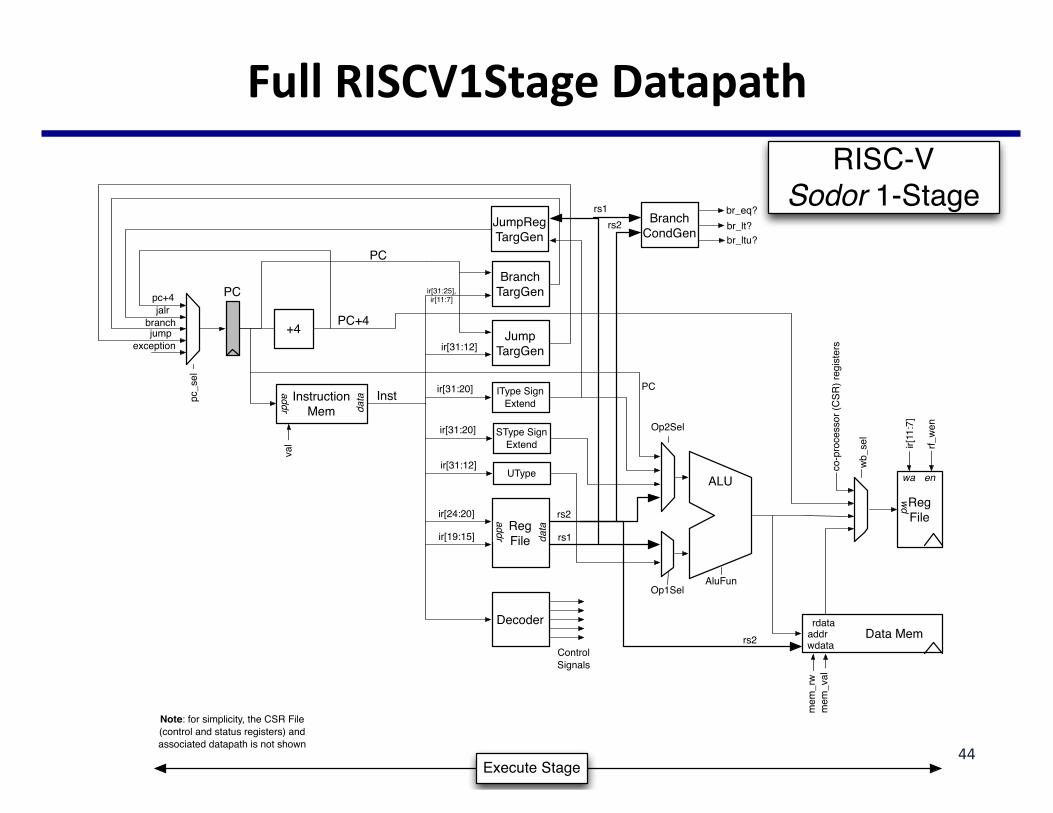
FullRISCV1StageDatapath
44
+4
Instruction Mem
RegFile
IType SignExtend
DecoderData Mem
ir[24:20]
branch
pc+4
pc_s
el
ir[31:20]
rs1
ALU
ControlSignals
wb_s
el
RegFile
rf_we
n
val
mem
_rw
PC
mem
_val
addrwdata
rdata
Inst
JumpTargGen
BranchTargGen
ir[19:15]
ir[31:25],ir[11:7]
PC+4jalr
rs2
BranchCondGen
br_eq?br_lt?
co-p
roce
ssor
(CSR
) reg
ister
s
ir[11
:7]
jump
ir[31:12]
Execute Stage
br_ltu?PC
addr
ir[31:12]
JumpRegTargGen
Op2Sel
Op1SelAluFun
data
wa
wd
en
addr data
UType
Note: for simplicity, the CSR File (control and status registers) and associated datapath is not shown
RISC-V Sodor 1-Stage
exception
SType SignExtend
ir[31:20]
PC
rs2rs1
rs2

AdditionalMaterials
45

LogicDesignBasics
• Informationencodedinbinary– Lowvoltage=0,Highvoltage=1– Onewireperbit– Multi-bitdataencodedonmulti-wirebuses
• Combinationalcircuit– Operateondata– Outputisafunctionofinput
• State(sequential)circuit– Storeinformation
46

CombinationalCircuits
• AND-gate– Y=A&B
AB Y
I0I1 Y
Mux
S
n Multiplexern Y=S?I1:I0
A
BY+
A
B
YALU
F
n Addern Y=A+B
n Arithmetic/LogicUnitn Y=F(A,B)
47

Sequential Circuits
• Register: stores data in a circuit– Uses a clock signal to determine when to update the
stored value– Edge-triggered: update when Clk changes from 0 to 1
D
Clk
QClk
D
Q
48

Edge-TriggeredDFlipFlops
• ValueofDissampledonpositiveclockedge.
• Qoutputs sampled value forrestofcycle.
D Q
CLK
D
Q
49
Sequential Circuits
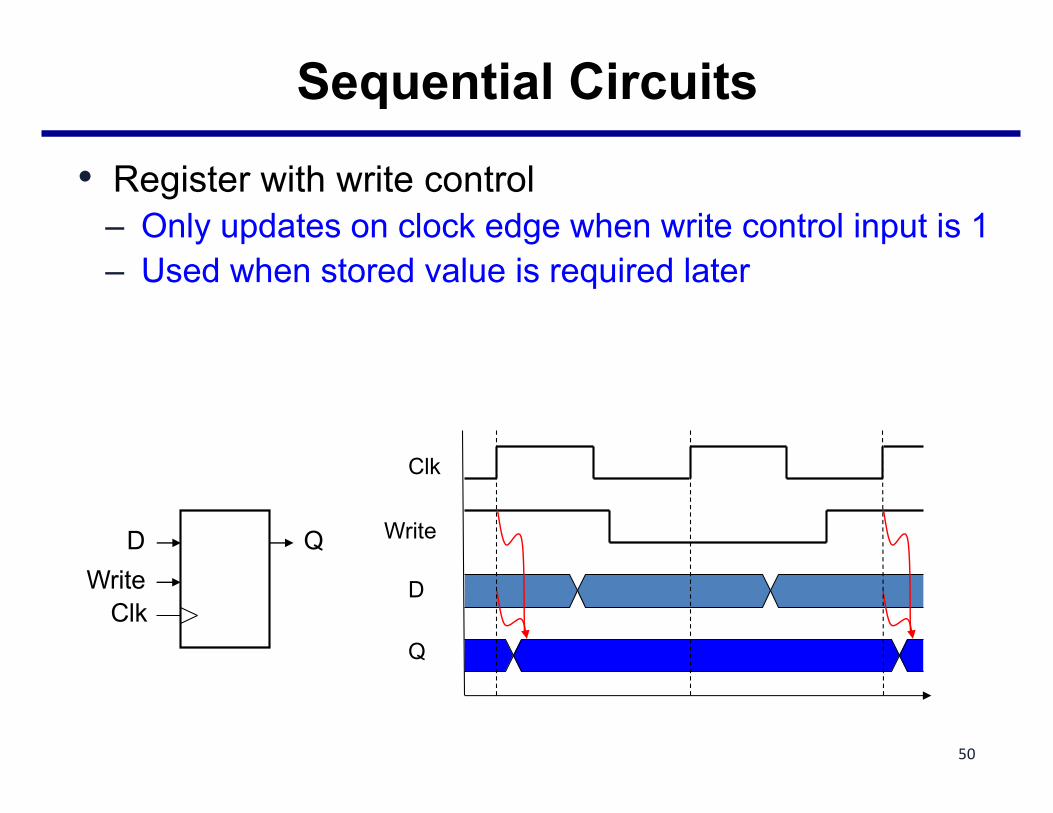
• Register with write control– Only updates on clock edge when write control input is 1– Used when stored value is required later
D
Clk
QWrite
Write
D
Q
Clk
50

Clocking Methodology• Combinational logic transforms data during clock
cycles– Between clock edges– Input from state elements, output to state element– Longest delay determines clock period
51

Singlecycledatapaths
Processorusessynchronouslogicdesign(a“clock”). f T
1 MHz 1 μs10 MHz 100 ns100 MHz 10 ns
1 GHz 1 ns
Allstateelementsactlikepositiveedge-triggeredflipflops.
D Q
clk
Reset ?
52

Single-CycleHardwiredControl
Clockperiodissufficientlylongforallofthefollowingstepstobe“completed”:1. Instructionfetch2. Decodeandregisterfetch3. ALUoperation4. Datafetchifrequired5. Registerwrite-backsetuptime
=>tC >tIFetch +tRFetch +tALU+tDMem+tRWB
Attherisingedgeofthefollowingclock,thePC,registerfileandmemoryareupdated
53

ALUControl&ImmediateExtension
54
Inst<6:0>(Opcode)
DecodeMap
Inst<14:12> (Func3)
ALUop
0?
+
FuncSel(Func,Op,+,0?)
ImmSel(IType12,SType12,UType20)