leakage and dynamic glitch power minimization using mip for v th assignment and path balancing...
TRANSCRIPT
Leakage and Dynamic Glitch Power Minimization Using MIP
for Vth Assignment and Path Balancing
Yuanlin Lu and Vishwani D. AgrawalAuburn University
ECE Dept., Auburn, Alabama, USA
PATMOS’05, Leuven, Belgium, September 21-23, 2005
2
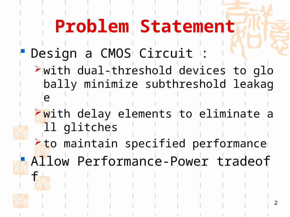
Problem Statement Design a CMOS Circuit :
with dual-threshold devices to globally minimize subthreshold leakage
with delay elements to eliminate all glitches to maintain specified performance
Allow Performance-Power tradeoff

3
CL
Dynamic Switching Power Dynamic Switching Power ++ Short Circuit Power Short Circuit Power ++ Leakage PowerLeakage Power
Power Consumption in CMOS Circuits
4
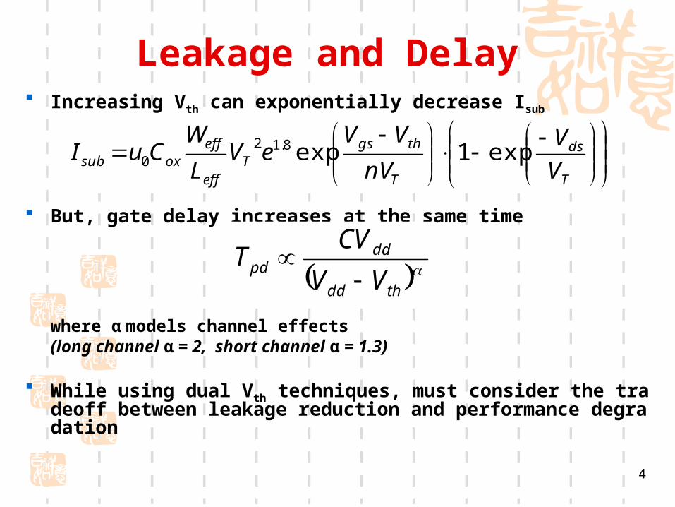
Leakage and Delay Increasing Vth can exponentially decrease Isub
But, gate delay increases at the same time
where α models channel effects(long channel α = 2, short channel α = 1.3)
While using dual Vth techniques, must consider the tradeoff between leakage reduction and performance degradation
thdd
ddpd
VV
CVT
T
ds
T
thgsT
eff
effoxsub V
V
nV
VVeV
L
WCuI exp1exp8.120

5
Some Previous References on Leakage Reduction and Glitch Power Reduction
Leakage Power Minimization by Dual-Vth CMOS Devices Heuristic Algorithms (locally optimal solution)
Q. Wang and S. B. K. Vrudhula, "Static Power Optimization of Deep Submicron CMOS Circuits for Dual VT Technology," Proc. ICCAD, 1998, pp. 490-496.
L. Wei, Z. Chen, M. Johnson and K. Roy, “Design and Optimization of Low Voltage High Performance Dual Threshold CMOS Circuits,” Proc. DAC, 1998, pp. 489-494.
Linear Programming (globally optimum solutions) D. Nguyen, A. Davare, M. Orshansky, D. Chinney, B. Thompson and K. Keu
tzer, “Minimization of Dynamic and Static Power Through Joint Assignment of Threshold Voltages and Sizing Optimization,” Proc. ISLPED, 2003, pp. 158-163.
F. Gao and J. P. Hayes, “Gate Sizing and Vt Assignment for Active-Mode Leakage Power Reduction,” Proc. ICCD, 2004, pp. 258-264
Dynamic Glitch Power Elimination by Linear Programming T. Raja, V. D. Agrawal and M. L. Bushnell, “Minimum Dynamic Power CMO
S Circuit Design by a Reduced Constraint Set Linear Program,” Proc. 16th International Conference on VLSI Design, 2003, pp. 527-532.

6
New MIP: A Mixed Integer Linear Programfor Leakage and Glitch Power Reduction
Objective Function:
Minimize {Total leakage + No. of glitch
suppressing delay elements}
Alternative objective function (linear approximation):
Minimize {Total leakage + Total glitch
suppressing delay}

7
Objective Function
Minimize { Σ Xi ILi + (1-Xi)IHi all gates i
+ Σ Σ Δdij } all gates i→ j
Where Xi = 1, gate i has low Vth, leakage = ILi
Xi = 0, gate i has high Vth, leakage = IHi
Δdij = delay inserted between gates i and j
for glitch suppression
Xi = [0,1] is integer, Δdij is real variable
ILi and IHi are constants for gate i determined by SPICE
8
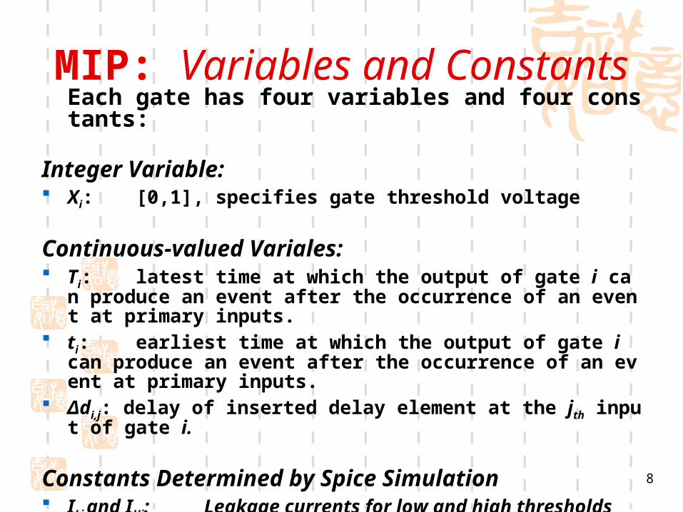
MIP: Variables and ConstantsEach gate has four variables and four constants:
Integer Variable: Xi: [0,1], specifies gate threshold voltage
Continuous-valued Variales: Ti: latest time at which the output of gate i can produce an
event after the occurrence of an event at primary inputs. ti: earliest time at which the output of gate i can produce a
n event after the occurrence of an event at primary inputs. Δdi,j: delay of inserted delay element at the jth input of gate i.
Constants Determined by Spice Simulation ILi and IHi: Leakage currents for low and high thresholds DLi and DHi: Delays for low and high thresholds
9
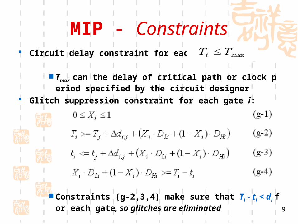
MIP - Constraints Circuit delay constraint for each PO i:
Tmax can the delay of critical path or clock period specified by the circuit designer
Glitch suppression constraint for each gate i:
Constraints (g-2,3,4) make sure that Ti - ti < di for each gate, so glitches are eliminated
10
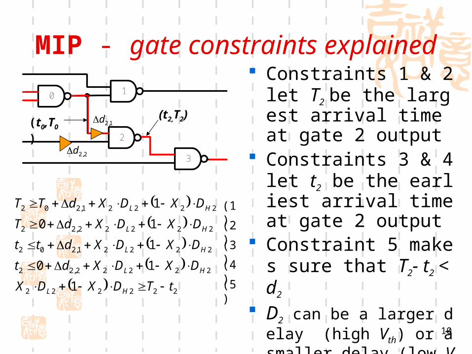
MIP - gate constraints explained Constraints 1 & 2 let T2
be the largest arrival time at gate 2 output
Constraints 3 & 4 let t2 be the earliest arrival time at gate 2 output
Constraint 5 makes sure that T2- t2 < d2
D2 can be a larger delay (high Vth) or a smaller delay (low Vth)
0
3
1
2
(t2,T2)(t0,T0) 1,2d
2,2d
222222
22222,22
22221,202
22222,22
22221,202
1
10
1
10
1
tTDXDX
DXDXdt
DXDXdtt
DXDXdT
DXDXdTT
HL
HL
HL
HL
HL
(1)
(2)
(3)
(4)
(5)

11
Power-Delay Tradeoff ExampleA 14-Gate Full Adder
A
B
C
Co
S
A
B
C
Co
S
A
B
C
Co
S
Unoptimized Circuit Optimized Circuit @ Tmax=Tc
Optimized Circuit @ Tmax=1.25 Tc
12
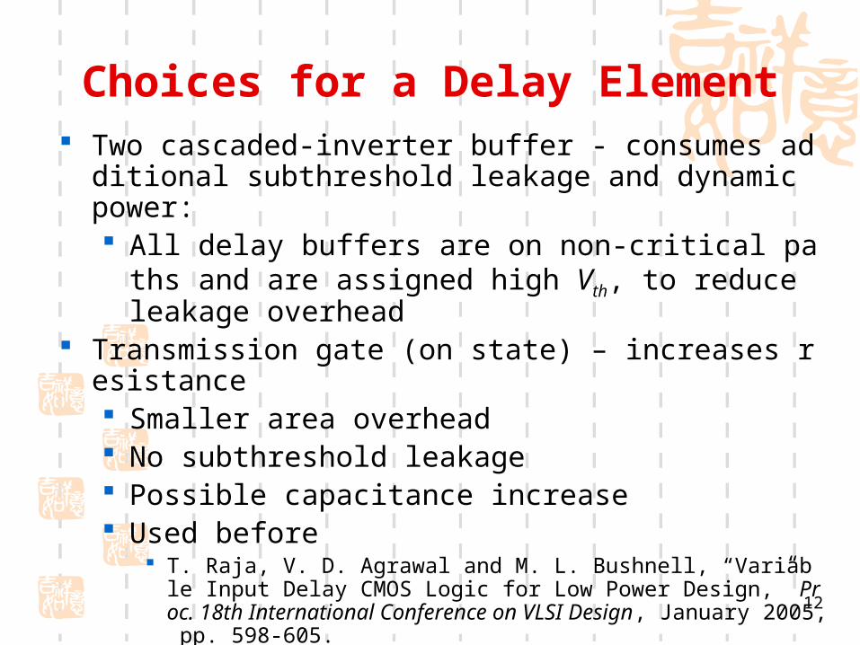
Choices for a Delay Element Two cascaded-inverter buffer - consumes additional subt
hreshold leakage and dynamic power: All delay buffers are on non-critical paths and are assi
gned high Vth, to reduce leakage overhead Transmission gate (on state) – increases resistance
Smaller area overhead No subthreshold leakage Possible capacitance increase Used before
T. Raja, V. D. Agrawal and M. L. Bushnell, “Variable Input Delay CMOS Logic for Low Power Design,” Proc. 18th International Conference on VLSI Design, January 2005, pp. 598-605.
T. Raja, V. D. Agrawal and M. L. Bushnell, “Variable Input Delay CMOS Logic Design for Low Dynamic Power Circuits,” PATMOS’05.

13
Delay Element Implementation
Buffer
(a)
Vdd
GND
1 1 000
Vdd
GND
0 1 1 0a
(b)
Gate LeakageSubthreshold
(a) Transmission Gate (b) Buffer
Delay Element SubthresholdLeakage (pA)
Transmission Gate
High Vth 0
Low Vth 0
Buffer (Two Cascaded Inverters)
High Vth 409
Low Vth 20800
* size of buffer:
W/L: N1:315/70
P1:630/70
N2:175/70
P2:350/70
14
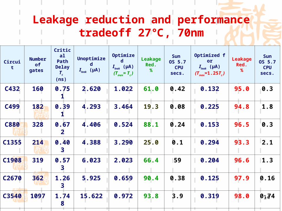
Leakage reduction and performance tradeoff 27 , 70nm℃
CircuitNumber
ofgates
CriticalPathDelay
Tc
(ns)
UnoptimizedIleak (μA)
Optimized Ileak (μA)
(Tmax= Tc )
LeakageRed.
%
Sun OS 5.7 CPUsecs.
Optimized forIleak (μA)
(Tmax=1.25Tc )
Leakage Red.
%
SunOS 5.7CPUsecs.
C432 160 0.751 2.620 1.022 61.0 0.42 0.132 95.0 0.3
C499 182 0.391 4.293 3.464 19.3 0.08 0.225 94.8 1.8
C880 328 0.672 4.406 0.524 88.1 0.24 0.153 96.5 0.3
C1355 214 0.403 4.388 3.290 25.0 0.1 0.294 93.3 2.1
C1908 319 0.573 6.023 2.023 66.4 59 0.204 96.6 1.3
C2670 362 1.263 5.925 0.659 90.4 0.38 0.125 97.9 0.16
C3540 1097 1.748 15.622 0.972 93.8 3.9 0.319 98.0 0.74
C5315 1165 1.589 19.332 2.505 87.1 140 0.395 98.0 0.71
C6288 1177 2.177 23.142 6.075 73.8 277 0.678 97.1 7.48
C7552 1046 1.915 22.043 0.872 96.0 1.1 0.445 98.0 0.58
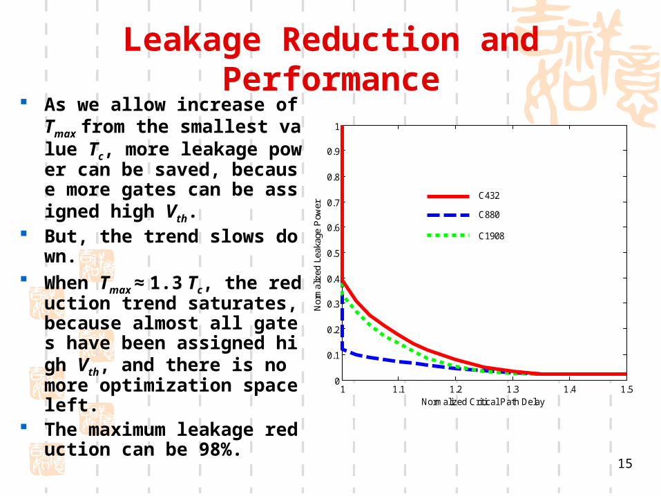
15
Leakage Reduction and Performance As we allow increase of Tmax fr
om the smallest value Tc, more leakage power can be saved, because more gates can be assigned high Vth.
But, the trend slows down. When Tmax ≈ 1.3 Tc, the reducti
on trend saturates, because almost all gates have been assigned high Vth, and there is no more optimization space left.
The maximum leakage reduction can be 98%.
1 1.1 1.2 1.3 1.4 1.50
0.1
0.2
0.3
0.4
0.5
0.6
0.7
0.8
0.9
1
Normalized Critical Path Delay
Nor
mal
ized
Lea
kage
Pow
er
C432
C880
C1908

16
Comparing Dynamic & Leakage Power Leakage (increases with temperature):
Determined by Spice simulation of gates at 90ºC Added up for all gates of circuit optimized by MIP
Dynamic power (depends on node activity and capacitance): Node capacitances for optimized circuit estimated Gate delays determined by Spice simulation of gates Activity determined by event driven discrete-time simulato
r using 1,000 random vectors applied with 120% Tc clock period
c
ii
iddinvdyn
dyn T
FOTVC
T
EP
2.11000
5.0 2

17
Leakage, Dynamic and Total Power Comparison 90 , 70nm℃
CircuitName
No. of
Gates
Leakage Power Dynamic Power Total Power
Pleak1
(uW)
Pleak2 (u
W)Leakage
Reduction Pdyn1 (u
W)
Pdyn2 (u
W)Dynamic
Reduction Ptotal1
(uW)
Ptotal2
(uW)Total
Reduction
C432 160 35.77 11.87 66.8% 101.0 73.3 27.4% 136.8 85.2 37.7%
C499 182 50.36 39.94 20.7% 225.7 160.3 29.0% 276.1 200.2 27.5%
C880 328 85.21 11.05 87.0% 177.3 128.0 27.8% 262.5 139.1 47.0%
C1355 214 54.12 39.96 26.3% 293.3 165.7 43.5% 347.4 205.7 40.8%
C1908 319 92.17 29.69 67.8% 254.9 197.7 22.4% 347.1 227.4 34.5%
C2670 362 115.4 11.32 90.2% 128.6 100.8 21.6% 244.0 112.1 54.1%
C3540 1097 302.8 17.98 94.1% 333.2 228.1 31.5% 636.0 246.1 61.3%
C5315 1165 421.1 49.79 88.2% 465.5 304.3 34.6% 886.6 354.1 60.1%
C6288 1189 388.5 97.17 75.0% 1691.2 405.6 76.0% 2079.7 502.8 75.8%
C7552 1046 444.4 18.75 95.8% 380.9 227.8 40.2% 825.3 246.6 70.1%
18
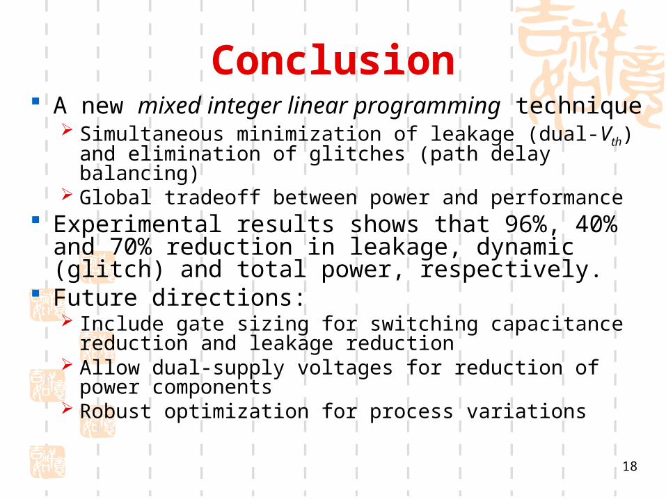
Conclusion A new mixed integer linear programming technique
Simultaneous minimization of leakage (dual-Vth) and elimination of glitches (path delay balancing)
Global tradeoff between power and performance Experimental results shows that 96%, 40% and
70% reduction in leakage, dynamic (glitch) and total power, respectively.
Future directions: Include gate sizing for switching capacitance reduction a
nd leakage reduction Allow dual-supply voltages for reduction of power
components Robust optimization for process variations

Thank You All !
Questions?