layout of 7400-series chips commonly used in cda 3101
TRANSCRIPT

Layout of 7400-series ChipsCommonly Used in
CDA 3101: Introduction to ComputerHardware and Organization
Charles N. Winton
Department of Computer and Information SciencesUniversity of North Florida
1999

Vcc
14 13 12 11 10 9 8
7654321GND
7400: QUAD 2-INPUT NAND

14 13 12 11 10 9 8
7654321GND
Vcc
7410: TRIPLE 3-INPUT NAND

14 13 12 11 10 9 8
7654321GND
7420: DUAL 4-INPUT NAND
Vcc

14 13 12 11 10 9 8
7654321GND
Vcc
7430: 8-INPUT NAND

14 13 12 11 10 9 8
7654321GND
Vcc
7402: QUAD 2-INPUT NOR

14 13 12 11 10 9 8
7654321GND
Vcc
7427: TRIPLE 3-INPUT NOR
14 13 12 11 10 9 8
7654321GND
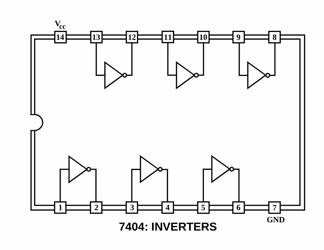
7404: INVERTERS
Vcc
14 13 12 11 10 9 8
7654321GND
Vcc
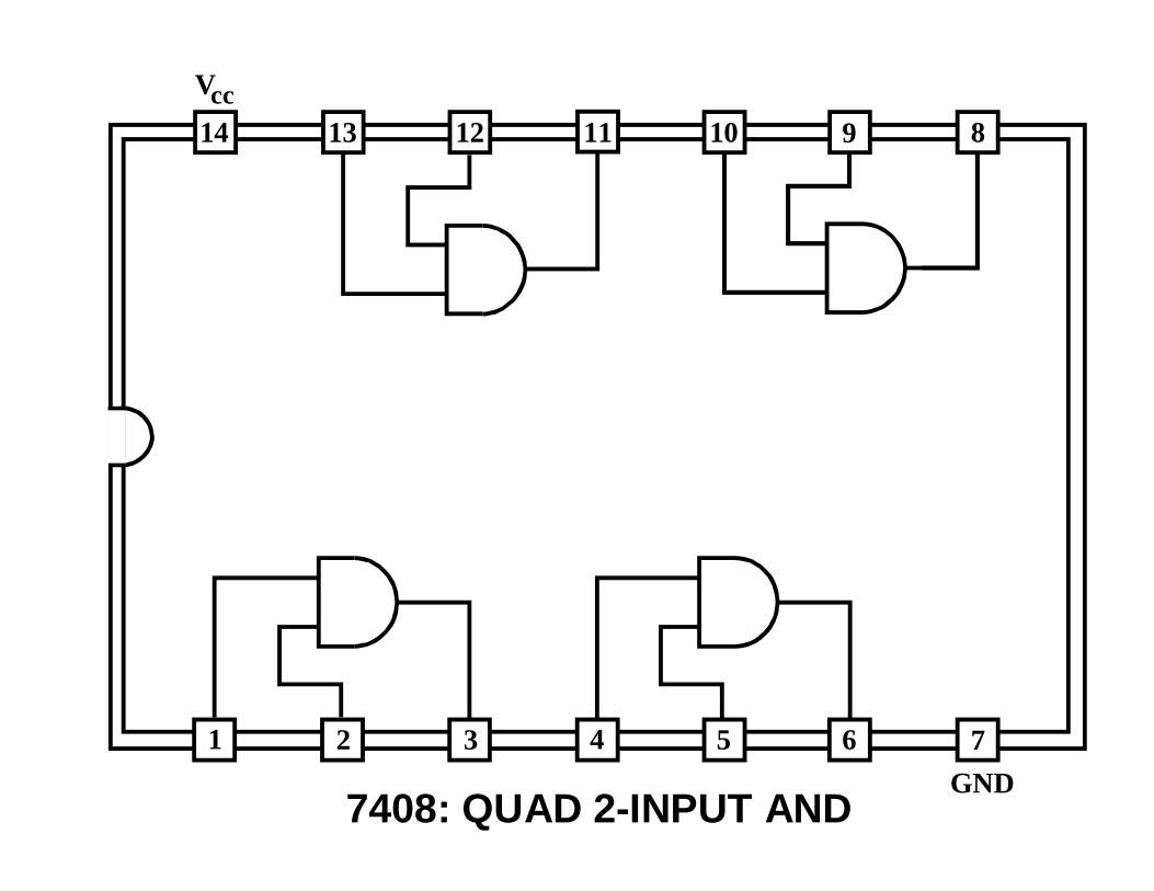
7408: QUAD 2-INPUT AND
14 13 12 11 10 9 8
7654321GND
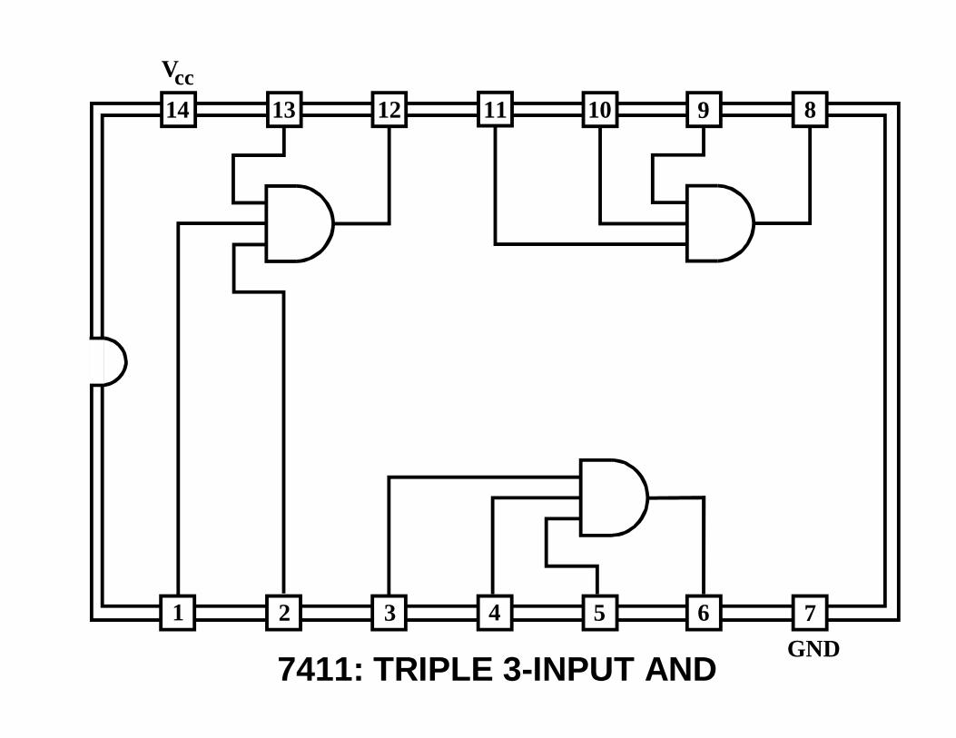
7411: TRIPLE 3-INPUT AND
Vcc

14 13 12 11 10 9 8
7654321GND
7421: DUAL 4-INPUT AND
Vcc

14 13 12 11 10 9 8
7654321GND
Vcc
7432: QUAD 2-INPUT OR

14 13 12 11 10 9 8
7654321GND
Vcc
7486: QUAD 2-INPUT XOR

14 13 12 11 10 9 8
7654321GND
Vcc
7451: DUAL 2-WIDE 2-INPUT AOI
Make No External Connection

GND
14 13 12 11 101516 9
87654321
Vcc
Data Inputs
Data Inputs
74151: 8-INPUT MULTIPLEXER
Enable
274 465
3 2 1 0
Address Inputs
Output Output
1
Active on Enable LOW(otherwise Output
is HIGH)

A = 1, B = 2, C = 4, D = 8Selected output goes LOW
GND
14 13 12 11 101516 9
87654321
Vcc
A B C D 9 8 7
0 1 2 3 4 5 6
Outputs
OutputsInputs
7442: 4 TO 10 LINE BCD TO DECIMAL DECODER

Selected output goes LOW
GND
14 13 12 11 101516 9
87654321
Vcc
f g a b c d e
B C D A
Inputs
Outputs (15V)
7447: BCD TO 7-SEGMENT DECODER DRIVER
a
b
c
d
e
f g
B=2C=4
D=8A=1
InputsLampTest
BI/RBI RBI
The ripple blanking inputs(BI and BI/RBI) arenormally held HIGH(they provide for zerosuppression). Lamp TestLOW selects all segments.

GND
14 13 12 11 101516 9
87654321
Vcc
Select
Data Outputs
74138: 3 TO 8 DECODER/DEMULTIPLEXEREnable
5430 621
A B CTie toLOW G1 7
DataOutput
When enable input G1 is HIGH, a binaryinput on Select inputs C, B, A turns thecorresponding output line LOW (theremaining output lines are HIGH). The outputselected is based on C=4, B=2, A=1. When G1is LOW, all the output lines are HIGH.
Tie toLOW

GND
14 13
1211
151618 1720 19
10987654321
21222324
Vcc
When enable inputs G2 and G1 are both LOW, abinary input on Select inputs D, C, B, A turns thecorresponding output line LOW (the remainingoutput lines are HIGH). The output selected isbased on D=8, C=4, B=2, A=1. When either G2 orG1 is HIGH, all the output lines are HIGH.
A B D G2
7
74154: 4 TO 16 LINE DECODER
Select Enable Outputs
5430 621
Outputs
C G1
8 9 10
1112131415
GND
14 13 12 11 101516 9
87654321
Vcc
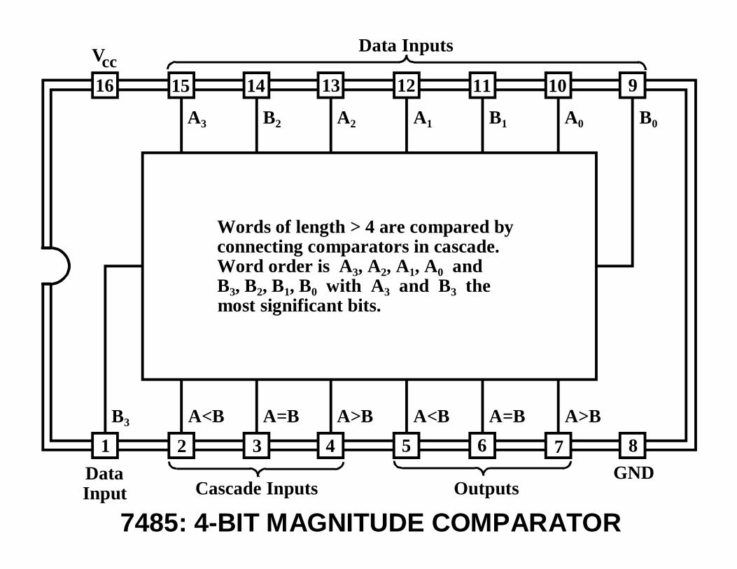
Cascade Inputs
Data Inputs
7485: 4-BIT MAGNITUDE COMPARATOROutputs
A0B1A1A3 B0A2B2
B3 A<B A=B A>B A<B A=B A>B
DataInput
Words of length > 4 are compared byconnecting comparators in cascade.Word order is A3, A2, A1, A0 andB3, B2, B1, B0 with A3 and B3 themost significant bits.

14 13 12 11 10 9 8
7654321
7490: DECADE COUNTER
Input(A) Q0 GND
Reset Tie to 0Tie to Q0 Reset Tie to 0
Q3, Q2, Q1, Q0 are the state outputs of 4internal JK Master-Slave flip-flopsconnected as a standard BCD counter.To reset to 0 both Resets must beHIGH. Pulse Input(A) for the BCD counting sequence. (There are alternateconnections to permit divide by 5 and9's complement support)
Q3 Q1 Q2
Vcc

14 13 12 11 10 9 8
7654321
7493: 4-BIT BINARY COUNTER
Input(A) Q0 GND
ResetTie to Q0 Reset
Q3, Q2, Q1, Q0 are the state outputs of 4internal JK Master-Slave flip-flopsconnected as a standard Mod 16counter. To reset to 0 both Resets mustbe HIGH. Pulse Input(A) for theMod 16 counting sequence. (There arealternate connections to permit divideby 2 and divide by 8 support)
Q3 Q1 Q2
Vcc

GND
14 13 12 11 101516 9
87654321
Vcc LoadOutputs
74193: 4-BIT BINARY UP/DOWN COUNTEROutputs
CCarryA DBorrow
B QB QACountDown QC QD
Pulse the Count Up or Count Down clock to producethe change of count on QD, QC, QB, QA (hold the clocknot in use HIGH). Setting data on D, C, B, A with Load LOW and then taking Load HIGH will presetthe counter. Likewise, taking Clear from LOW to HIGH will zero the counter. In cascading counters, forcounting up, the Carry goes to the Count Up of thenext counter; for counting down, the Borrow goes tothe Count Down of the next counter.
CountUp
Outputs InputsData
Data DataClear
(Presettable,Synchronous,Dual Clocks)

14 13 12 11 10 9 8
7654321GND
Vcc
74126: QUAD TRI-STATE BUFFER
C C
C C
BUFFER IS ACTIVE WHEN C IS HIGH

14 13 12 11 10 9 8
7654321GND
74243: QUADRUPLE BUS TRANSCEIVERGAB
GBAVcc
GAB = HGBA = H
B1 B2 B3 B4
A1 A2 A3 A4
GAB = LGBA = L
GAB = HGBA = L
ISOLATEDIF

GND
14 13 12 11151618 1720 19
10987654321
Vcc
74244: OCTAL TRI-STATE BUFFERS/LINE DRIVERSG(1) A1(1) B1(2) A2(1) B2(2) A3(1) B3(2) A4(1) B4(2)
G(2) B1(1) A1(2) B2(1) A2(2) B3(1) A3(2) B4(1) A4(2)

14 13 12 11 10 9 8
7654321
GND
7473: DUAL JK MASTER-SLAVE FLIP-FLOP
Q Q
Q Q
J
K
J
KCLR CLR
J(1) Q(1) Q(1) K(2) Q(2) Q(2)
K(1) J(2)Clock(1) Clear(1) Clock(2) Clear(2)
(NEGATIVE EDGETRIGGERED
WITH CLEAR)
Vcc

Q
14 13 12 11 10 9 8
7654321GND
7474: DUAL D FLIP-FLOP
Q
Q
QD
D
PR CLR
Set(1) Q(1)Q(1)
D(2) Q(2) Q(2)
D(1)
Set(2)
Clock(1)Clear(1)
Clock(2)Clear(2)
CLR PR
(WITH PRESET & PRECLEAR)
(POSITIVE EDGE TRIGGERED)
Vcc

14 13 12 11 101516 9
87654321
7476: DUAL JK MASTER-SLAVE FLIP-FLOP
GNDK(1) J(2)
Clock(1) Clear(1) Clock(2) Clear(2)J(1)
Q(1)Q(1) K(2) Q(2) Q(2)
Set(1) Set(2)
Q
Q
J
KCLR
CK
PRQ
Q
J
KCLR
CK
PR
(WITH PRESET AND PRECLEAR, NEGATIVE EDGE TRIGGERED)
Vcc

14 13 12 11 101516 9
87654321
7483: 4-BIT BINARY FULL ADDER W/FAST CARRY
GNDB3 S3
AdderA3
B3
CI3CO3S3
COUT CIN B0 A0 S0
A3 S2 A2 B2 S1 B1 A1
AdderA0
B0
CI0CO0S0
AdderA2
B2
CI2CO2
S2
AdderA1
B1
CI1CO1S1
Vcc

For a right shift, set Mode Control LOW andpulse the Shift Right input. The shift directionis Serial Data QA QB QC QD .For a parallel load from the inputs A, B, C, Dset Mode Control HIGH then pulse the Loadinput. A shift left requires connecting QB to A,QC to B, QD to C, and the Serial Input to D, then executing a parallel load.
14 13 12 11 10 9 8
7654321
7495: 4-BIT BIDIRECTIONAL PARALLEL SHIFT REG
Parallel Outputs
GND
ShiftRight
Load
Parallel InputsSerialInput
ModeControl
QA QB QC QD
A B C D
Vcc

GND14 13 12 11 101516 9
87654321
Vcc
2102: 1K x 1-BIT STATIC RAM - Vcc = +5VA1 A2 A3 A4A6 A5 A0
A7 A8 A9 CS
WE
DOUT DIN

GND
14 13 12 11 10
987654321
151618 17Vcc
2114: 1K x 4-BIT STATIC RAM - Vcc = +5VA1 A2A3A4A6 A5 A0 CS
A7 A8 A9 WEI/O1 I/O2 I/O3 I/O4

DATA
2-INPUT MULTIPLEXER
SELECT z
GNDINPUTS
x I1 I0 z z
+5V: VCC
7404: NOT7432: OR7408: AND
x
I1I0
z
University of North FloridaDepartment of Computer and Information Sciences
Breadboard Template, 1999
OUTPUTS

University of North FloridaDepartment of Computer and Information Sciences
Breadboard Template, 1999