lasers for the to 15,0 micrometer spectral region
TRANSCRIPT

NASA CONTRACTOR REPORT 145259
1 PbsLSEAEVARCMDB flXVXjo_NBN1BSi ICCHDUCTOB LASIRS 10R THE 80OF N7-2 0I5a ETE SIPCTLAL BEGICD FinaaRHeport ifascr Aralytics Inc lexingtonUCzp_-A- A01 -Uncas
ADVANCED DEVELOPMENT OF PB-SALT SEMICONDUCTOR
LASERS FOR THE 80 TO 150 MICROMETER
SPECTRAL REGION
KURT JLINDEN JACK FBUTLER KENNETH WNILL
LASER ANALYTICS INC 38 HARTWELL AVENUE LEXINGTON MASSACHUSETTS 02173
CONTRACT NAS1-14448 OCTOBER 1977
AAO19 _
NASA National Aeronautics and Space Administration
Langley Research Center Hampton Virginia 23665
FINAL REPORT
ADVANCED DEVELOPMENT OF Ph-SALT
SEMICONDUCTOR LASERS FOR THE
80 TO 150 MICROMETER
SPECTRAL REGION
NASA Contractor Report 145259
Contract NASl-14448
Submitted to
National Aeronautics and Space Administration Langley Research Center Hampton Virginia 23665
Dr Frank Allario Contract Monitor
by
Laser Analytics Inc 38 Hartwell Avenue
Lexington Massachusetts 02173
---
TABLE OF CONTENTS
10 INTRODUCTION
11 Program Objectives
12 General Approach
13 Summary of Results
20 CRYSTAL GROWTH AND MATERIALS PREPARATION
21 Crystal Growth-Methods
211 General Description
212 Procedures
213 Growth Furnace Characteristics
214 Residual Gas Pressure Effects
215 Purification by Binary Sublimation
216 Summary of Crystal Growth Runs
22 Compositional Interdiffusion (CID)
221 Background
222 Techniques Employed
223 Experimental Verification of the CID Process
224 Lattice Matching Experiment
23 Pn Junction Diffusion
30 DEVICE FABRICATION
ORIGAL A OF POOR QUALM31 Crystal Processing
32 Stripe Formation and Diffusion
33 Metallization
34 End-Face Cleaving
35 Chip Mounting in Packages
36 Experimental Package Study
40 LASER EVALUATION
41 Evaluation Methods
411 Dip-stick testing for Electrical Characterization
412 Evaluation of Emission Characteristics
4121 Spectral Characteristics
4122 Spatial Profile Measurements
42 Electrical and Optical Performance Results of Lasers
Delivered to NASA Langley Research Center
421 Laser No 7028-6
422 Laser No 6271-2
423 Laser No 7067-5
424 Laser No 7067-7
425 Laser No 7075-12
426 Laser No 7109-6
427 Laser No 7111-3
428 Laser No 7061-1
429 Laser No 7069-1
43 Summary and Discussion of Laser Performance Data
44 Reliability and Lifetime Studies
441 Package Relaxation
442 Crystal Degradation
443 Low Temperature Storage and Operation
444 Discussion
50 RECOMMENDATIONS FOR FURTHER WORK
51 Results
52 Recommendations
-iishy
60 REFERENCES
APPENDIX A Single Heterostructure Lasers of PbSlxSex and
Pb xSnxSe With Wide Tunability K J Linden
K W Nil and J F Butler
-1ii1shy
10 INTRODUCTION
11 Program Objectives
The objective of this program was to develop the techshy
nology for producing Pb-salt diode lasers for the 8-15 pm spectral
region suitable for use as local oscillators in a passive Laser
Heterodyne Spectrometer (LHS) Consideration was given to long
range NASA plans for the utilization of the passive LHS in a
space shuttle environment Specific goals included 1) achievement
of a power output of 05 milliwatts per mode 2) detailed evaluashy
tion of laser characteristics and 3) delivery of lasers to NASA
Langley Research Center for evaluation
12 General Approach
The general approach was to further develop the method
of Compositional Interdiffusion (CID) recently reported by Laser
Analytics Inc and used successfully at shorter wavelength [11
This technology has been shown to provide an effective and reshy
producible method of producing a single-heterostructure (SH) diode
of either the heterojunction or single-sided configuration The
program included refinements in crystal growth and materials proshy
cessing techniques investigations into new fabrication methods
and a study of temperature cycling and lifetime problems
13 Summary of Results
Performance specifications were exceeded in several
devices with single-ended CW power outputs as high as 088 millishy
watts in a mode being achieved The majority of the CID lasers
fabricated during the program had CW operating temperatures of
over 60K 30 of them operated CW above the boiling temperature
-1shy
of liquid nitrogen CW operation above liquid nitrogen temperashy
ture was possible for wavelengths as long as 103 pm Operation
at 77K is significant with respect to space shuttle operations
since it allows considerable simplification of cooling methods
In addition to performance laser improvements the program inshy
cluded 1) an experimental verification of the CID effect which
resulted in valuable new insight into the CID process 2) a
study of reliability and failure modes and 3) investigations into
several specific new areas of materials processing and device
fabrication
The results of this program represent a substantial
improvement in the state-of-the-art of tunable diode lasers in
the 8-15 pm spectral range Previous homojunction lasers in
this spectral range have generally had maximum operating temperashy
tures below 40K have never exhibited 77K operation and have
consistently produced maximum CW power outputs of less than 05
milliwatts overall The CID technology can now be used on a
reproducible basis in both the PbSSe and the PbSnSe systems
-2shy
20 CRYSTAL GROWTH AND MATERIALS PREPARATION
21 Crystal Growth Methods
211 General Description
The standard crystal growth method used at Laser
Analytics (and thatused for crystals grown for this program)
is a closed tube ingot nucleation method whereby an evacuated and
sealed quartz ampoule containing a coarse crush of the desired
material composition is placed in a tubular furnace which has been
previously profiled to have the proper temperature distribution
for optimum crystal growth During the growth period (which
typically requires 3 to 4 days) sublimation vapor transport and
recrystallization results in the growth of a number of crystals
at various positions in the capsule usually directly on some of
the source crush These crystals are generally characterized by
planar facets (usually [1001-oriented) which are utilized in device
fabrication Such material has in the past been found to be of
high crystallographic quality with the as-grown facets exhibiting
dislocation densities in the 104 cm- 2 range prior to handling
212 Procedures
The crystal growth process involves the following
general steps
A Weighing of the elements
B Prereaction at approximately 1100C
C Loading of the prereacted ingots into growth
capsules
D Growth at 810-8300 C
-3shy
High purity (grade 69) Pb and Sn was obtained
from Cominco American The manufacturer supplied lot analyses
of all materials which indicated trace amounts of Bi Ca Sb
Cu Fe Mg Si and In each with 01 ppm or less Selenium was
purchased from Eagle Picher who also specify 69 purity (grade
UHP) All weighing was carried out using a Mettler HSl microshy
balance accurate to the nearest 000001 gm The elements were
weighed out according to the formula
(Pb1 xSn) 1+6 Se
where x determines the band gap of the material and 1+6 signifies
the deviation from stoichiometry (1+6=1 implies perfect stoichioshy
metry) Large deviations from stoichiometry can lead tocrystals
with either metal or chalcogenide inclusions As expected from
published equilibrium phase diagram data [2] the crystals
generally grow p-type regardless of the amount or type of stoishy
chiometric deviation of the source material After weighing
the elements were placed into previously vacuum fired quartz
ampoules evacuated baked and sealed off at approximately 10- 6
- 5to 10 Torr This prereaction ampoule was then placed into a
furnace and heated to approximately 1100 0 C (approximately 200C
above the liquidus temperature of pure PbSe) Prior to removal
from this prereaction furnace it was rocked in order to insure
proper mixing The capsule was then removed and either air or
water quenched to prevent any segregation which would be expected
to occur if slow-cooling were allowed
After opening the prereaction capsule the ingot
was crushed coarse-sieved (1-2 mm) and loaded into a previously
vacuum fired growth ampoule This ampoule was then vacuum baked -overnight and sealed off at approximately 10- 6 to 10 5 Torr Growth
was carried out with the sealed ampoules situated in tubular
growth furnaces discussed in the next section Growth times
were typically 3-5 days Cool-down of the ampoules was proshy
grammed at an average of rate of about 100 C per hour Figure 1
-4shy
I yltifltifS
X- ifs ltif gtg
igtifgt
I
4
I I
rireI
aaeutadz4olp-to
lto cy ta t xotrl ifgt
if laquo fiiltitffgtis i i
I
shows a view of the ampoule bakeout and seal off portion of the
crystal growing area
213 Growth Furnace Characteristics
Crystals were grown for the program in 64 cm
long tubular furnaces with 5 cm diameter bores External shunt
taps on the furnace allow temperature profiling There are four
growth furnaces in operation at Laser Analytics all of which
were used for this program Each of the growth furnaces is
profiled to provide a small gradient towards one end (the gradient
extending through the center of the furnace) In addition to the
programmed logitudinal profile these furnaces also contain small
(few degrees) radial and vertical gradients The radial composhy
nent is due to radiational losses through the ends of the furnaces
and can be influenced by the use of plugs of varying lengths
The vertical component is due to the presence of convection curshy
rents These small gradients are known to play an important
role in determining crystal properties [ 3 ] Small differences
in these various temperature gradients from one furnace to another
are believed to lead to small variations in crystal properties
such as size and growth rate from one run to another
214 Residual Gas Pressure Effects
As described in Section 211 the vapor growth
process involves the transport of molecular constituents in the
vapor phase In such a process the vapor pressure due to foreign
ingredients can be expected to play a major role if this pressure
is near that of the partial pressures of the binary constituents
Harman and McVittie [4 ] found that under closed-tube growth conshy
ditions the size of the grown crystals is larger if the residual
vapor pressure in the capsule is low The obvious concern also
exists that the foreign substance within the ampoule is incorshy
porated in the grown crystal to produce defects nonradiative
-5shy
recombination sites and other adverse features This residual
capsule vapor pressure is how routinely monitored at Laser
Analytics by opening all capsules after growth in a closed
vacuum chamber and measuring the increase in vapor pressure
Runs producing good crystals generally exibited room temperature
residual pressures of 03 to 3 Torr
It has been consistently found that crystals
grown in capsules giving residual room temperature pressures
of over 10 Torr have terraced surfaces with relatively little
useable material A 10 Torr capsule pressure at room temperature
corresponds to approximately 30 Torr at an 850 0C growth temperashy
ture Reference to the vapor pressure data of Figure 2 shows
that such a pressure is higher than that of the Pb-salt material
in the growth capsule whereas vapor pressures of I Torr at
850 0C are of the order of the Pb-salt vapor pressures Thus
capsules with residual vapor pressures below or around 1 Torr
allow for more vapor transport and thus would be expected to
yield larger crystal sizes Initial pregrowth capsule presshy
sures at room temperature were typically 10- 5 Torr The source of the residual gas pressure is-not known with certainty alshy
though it is strongly suspected to result from gases trapped in
microvoids in the source ingot and the ultimate source may be
the chemical elements This hypothesis was confirmed by results
of growth from sublimed binaries described in the next section
215 Purification by Binary Sublimation
Because of the apparentimportance of residual
capsule pressure in improving crystal quality the program inshy
cluded a preliminary investigation of binary sublimation as a
purification technique The general approach was to prepare
growth ingots of the binaries and subject them to a sublimation
regrowth step in sealed evacuated quartz ampoules The procedure
utilized a steep temperature gradient with the source at 800 0C
and recrystallization near room temperature
-6shy
0
o 0
0 0
0 T
0 0o
C C
010
TO To0
TO
0
14shy
0 i
0
000
QR
IINA
PA
GE IS
Figure
OR
5r
23
UL
TVapo
prssur b-slt mterals
ofvarous
PbO
an soeFaien lmns
In the time allocated for this investigation in
the present program only PbSe was sublimed and this was combined
with an ingot of SnSe prepared by usual methods (ingot 1184) The
first attempt at crystal growth using 1184 failed because of
extremely rapid transport to the coolest region of the growth
ampoule with consequent polycrystalline structure A second
run was made at a temperature 150 lower than the usual growth
temperature This resulted in good quality crystals which howshy
ever were n-type (G137) A p-skin was formed with a 400C difshy
fusion and lasers were fabricated from the crystal Laser action
was not observed in any of the devices apparently because of a
deep irregular junction
The main result of this experiment is that the
crystal growth rate was significantly increased by pre-subliming
the PbSe giving strong support to the hypothesis that growth
inhibiting residual gas resides in the growth ingot In order
to utilize sublimed binaries all growth CID and pn-junction
parameters and oven profiles would have to be reestablished
It was estimated that these adjustments would require more time
and costs than were available in the scope of the program Thereshy
fore binary sublimation was not further included as part of the
program although it is being pursued at a lower level by Laser
Analytics
216 Summary of Growth Runs
During this program a total of 18 binary or
ternary source ingots were prepared These ingots were used
either for crystal growth or for conversiondiffusion purposes
A summary of these ingots showing their composition (x-value)
ingot identification number purpose and crystal growth results
(where applicable) is shown in Table 1 Crystals G69 through 100
were grown in order to optimize both furnace growth and CID
parameters as well as to obtain material suitable for a wide
variety of laser frequencies
-7shy
--
--
Table 1
SUMMARY OF Pb xSnxSe INGOTS AND
CRYSTALS PREPARED OR USED DURING THE PROGRAM
Composition Growth (G) (x) Ingot No Or Purpose Growth Results
0042 187
0042 188
0026 189
0 193
0 I103
0031 1108
00125 1109
00321 1121
005 1122
0036 1128
0035 1130
0047 1140
0039 I144
0048 1184
0047 1192
0030 1193
0047 1200
0047 1204
0045 1233
00445 1247
G69
G70
G71
p-source
n-source
G83
G84
p-source
G95
G98
GI00
G106
G109
G137
G138
G1391
G142
G146
G156T
G196
fair
fair
fair
good
poor
good
good
good
good
quaternary
good
fair
fair
fair
good
good
good
This ingot was a quaternary source with composition
Pb0961Sn0039Te0005Se0995 perfectly lattice matched
to PbSe
This ingot was prepared from the binaries using sublimed PbSe
t These crystals were not grown on this program
amp -8-
Following growth the crystals were stored for
further processing Some of this processing involved annealing
of the crystals with other sources in order to achieve either
CID structures or pn-junctions As the growths were carried out
in avariety of furnaces and under slightly different conditions
somewhat different growth results were generally obtained Only
onegrowth resulted in poor unuseable crystals Fair crysshy
tals were generally either smaller than usual or had a number of
visible grain boundaries Good crystals were moderate in size
(at least 3 mm on aside) and exhibited few if any grain bounshy
daries
Crystal G106 was subjected to the CID process
and used in the fabrication of four high performance lasers deshy
scribed in Section 4 Its composition was chosen to provide
lasers at specific wavelengths of interest to NASA
Growths G138 G142 and G146 were intended to
be exact duplicates of G106 to demonstrate reproducibility
While G138 and G142 appeared to reproduce the growth process
adequately G146 grew n-type instead of p-type The reason for
this discrepancy is not known although it is suspected that it
resulted from an unknown donor impurity accidently introduced
during processing
G196 was grown to provide high performance
lasers at NASA specified wavelengths
-9shy
22 Compositional Interdiffusion (CID)
221 Background
The CID method was developed by Laser Analytics
as an alternative relatively simple method of forming heteroshy
structures without the use of liquid-phase-epitaxy (LPE) or
molecular beam epitaxy (MBE) techniques While the latter techshy
niques have shown promise for forming heterostructures in the Pbshy
salts [56] they are considerably more complex to carry out and
the resulting lasers have exhibited severe reliability and lifeshy
time problems [781
The essential idea of the CID method is to anshy
neal a crystal of PblxSnxSe (or other Pb-salt ternary compound)
in the presence of a Pb1ySny Se vapor source where yltx Outshy
diffusion of the more volatile SnSe from the surface then proshy
duces a surface layer deficient in SnSe and thus possessing a
wider bandgap than the bulk The resulting structure is a single
heterobarrier In combination with a pn-junction as illustrated
in Figure 3 this structure then comprises a single-sided
heterojunction The high p-concentration of the bulk region comshy
pared to the much lower n-concentration in the diffused layer
ensures efficient injection into the confinement regions between
the heterobarrier and pn-junction
222 Techniques Employed
The CID procedure is generally carried out with
as-grown crystals of Pb lxSnxSe sealed in pre-cleaned and vacuumshy
baked quartz ampoules with poly-crystalline source ingots of
desired composition The typical processing temperature is 6001C
with heterobarrier depth controlled by annealing time assuming
the depth is proportional-to the square root of annealing time
Cool-down to room temperature is accomplished by rapid airshy
quench
ISORIGNo0L PKGF
OF pOOR QUALITY-10-
REGION 1 REGION 21 REGION 3
N-CID N-BULK I P-BULK
METALILAYER IERMI
CONDUCTION BAND
VALENCE BAND
_I
AT I ON ITENSITY
I
O1G~E~PAGE~I~jTEDI II Y
TER
TRAT ION
Figure 3
xSnxSe CID laser with pn-junction deeper thanteel of Pb
t CID region All x-axes represent distance below surface
oj crystal
Pn-junction diffusion may be performed simulshy
taneously with heterobarrier formation by using a source ingot
of opposite carrier type from the bulk Since the junction
movement proceeds by the rapid interdiffusion process whereas
the composition changes by self-diffusion the junction depth is
expected to be deeper than the heterobarrier as desired
223 Experimental Verification of the CID Process
To verify the occurance the CID effect and obtain
useful design parameters an electron beam microprobe (EBM) analyshy
sis was made of a CID-prepared structure The composition of the
as-giown p-type crystal before CID was Pb0955Sn0045 Se It
was sealed as described above with a source ingot of chalcogenideshy
rich Pb099Sn00 0 1 Se and annealed for six hours at 600C The
crystal has then cleaved and polished on a plane perpendicular
to the surface and microprobed along the polished face from the
surface into the bulk region Results of this EBM analysis are
shown in Figure 4 The existence of the CID effect is clearly
evident in that the composition of the crystal has been changed
to that of the source ingot for a distance extending approximately
5 pm into the bulk The apparent 2 pm width of the transistion
region represents the resolution limit of the microprobe
A diffusion coefficient is easily calculated
from the results of Figure 4 assuming that the diffusion depth
DDwhere t = the diffusion time and D the diffusion coefficient-11 2 The result is D = 12 x 10 cm sec The self-diffusion coeffishy
cient of Pb in Se-saturated PbSe at the same temperature obtained 10- 1cm by radioactive trace techniques was reported to be 16 x
sec [9] The close correspondence-of these results gives excelshy
lent support to the hypothesis that the CID effect results from
the self-diffusion of the metal constituent
-1shy
100
90
PbSe
801 region of SnSe outshydiffusion I
4-
4-I bulk
955 0 4 5 0o
20
SnSe 10
0 2 4 6 8 10 12 14
distance below surface (pm)
Figure 4 Composition vs distance into wafer for a Pb 955Sn 045Se
crystal interdiffused with Pb 0 9 9 9 Sn 0 0 0 1 Se at 6000C for 6
hours
Or P9
It is significant to note that the self-diffusion
coefficient of Pb in Pb-saturated PbSe is more than two ordersshy
of-magnitude less than that in Se-saturated PbSe Thus it is
expected that the heterobarrier depth in n-type material will be
much shallower than p-type
224 Lattice Matching Experiment
One aspect of heterostructure design to be conshy
sidered is the possibility of lattice mismatch between the layers
of different composition This may lead to strains and defects
within the crystal hence to device degradation Figure 5
shows the lattice constant variation for PblxSnxSe with
0 lt x lt 01 [1011] For the example of Figure 4 it may be
seen that the mismatch is less than 01 and even for Ax=0l
is only 016 From experience with III-V compound lasers [12]
mismatches of this magnitude would not be expected to be a problem
but the possibility cannot be overlooked
Attention was given to the potential lattice
mismatch problem in that a perfectly lattice matched structure
was fabricated This structure was achieved by utilizing the
fact that the two ternary systems Pbl xSnxSe and PblxSnxTe are
completely miscible over most of their composition range and
the addition of Te produces a larger lattice constant without
a significant change in bandgap This is illustrated in
Figure 6 which shows the lattice constant vs composition x y
for the quaternary system PblxSnxTelySey [1314] A large
range of perfectly lattice matched structures can be achieved In the work described here a PblxSnxTe ySey composition was
chosen to give emission near 12 pm and be perfectly lattice
matched to PbSe This composition was Pb096Sn0039Te0005Se0995
(as indicated in Table 1) and an ingot of this composition (G109)
was vapor grown The details of this lattice match are shown in
Figure 7 which is a blow-up of the lower right hand corner
of Figure 6 This crystal was interdiffused with PbSe to give
the lattice matched structure Point A represents the composition
-12shy
9 I613 -
1175CMEG
-o EG 810 cm
~E G =525 cm-1
= 612 U
611 0 02 04 06 08 01
x
Figure 5
Lattice constant (300K) of the Pb xSn xSe system for
0 lt x _ lt _ 01 E g values shown are at 12K
CM oO O
65LO If C3 L Pb Te
to0 64 - L
64 z
z Snco 62
0xwX 60
10 8 6 4 2 0
RPb- x SnxTe1y Se y
Figure 6 Lattice constant of the quaternary system PbJxSnxTel1ySey
showing iso-energy gap lines superimposed
6140 0
o IN
0610 0I-0C1
Co
0lt0
z 0 6120 X
_o 6110 Pb I Sn xTea S1yII-- - -
I-I
6100 1
010 005 0
Figure 7
Enlarged PbSe-corner of Figure 6 showing perfect lattice
matching between 12 pm quaternary material and pure PbSe
ORIGINAL PAGishyoF PoOR QUALUX
of ingot G109 while Point B represents the interdiffusediPbSe
region
Crystals of moderate size were grown from G109
Under microscopic examination large numbers of low-angle grain
boundaries were observed on the as-grown surfaces The cleavage
properties of the crystals were extremely poor and devices
fabricated from this did not exhibit laser action In view of
these poor initial results and NASAs expressed interest in obshy
taining high performance devices in a relatively short time
period this approach was not further pursued
23 Pn-Junction Diffusion
Pn-junction formation for this program was based on
control of stoichiometry deviations without the use of foreign
impurities For diffusion into p-type Pb1 -xSnxSe crystals the
vapor source was metal-saturated Pb1 -xSnxSe Movement of the
junction proceeds by interdiffusion which is generally orders
of magnitude faster than the self-diffusion mechanism governing
the CID process This difference in rates between the CID and
3unction diffusion processes makes it possible to control the
heterobarrier and pn-junction depths separately
Junction diffusions were carried out in evacuated
sealed quartz ampoules with the source ingot retained in an
inner quartz container to prevent physical contact with the -crystal Diffusion temperatures were in the range of 400o
600 0C and diffusion times from one to several hours Diffusion
depths were estimated from published values of interdiffusion
coefficients for the same condition [-9] In a number of cases
crystals were deliberately converted to opposite type using the
diffusion process Table 2 summarizes diffusion runs and conshy
versions carried as part of or in connection with this program
-13shy
Table 2 summarizes the diffusion runs and convershy
sions carried out in this program The original crystal growth
numbers are included as are performance characteristics of
lasers fabricated from these runs
OF
-14shy
Table 2
DIFFUSION RUN PARAMETERS
Growth
G No x-Value
95 0050
106 0047
138 0047
139 0030
142 0047
146 0047
156 0045
196 00445
D No
184
201
217
286
259
262
297
258
343
367
295
298
312
334
296
Diffusion
Type
Junction
Junction
Junction
Junction
Junction
Conversion
Junction
Junction
Conversion
Junction
Junction
Conversion
Junction
Junction
Junction
0 T(C) t(hr)
600 1
600 1
600 1
600 1
600 1
550 240
600 1
600 1
550 120
400 1
425 1
600 144
400 1
400 1
400 1
ORIGINAL PAGE IS OF POOR QUALITY
-15shy
30 DEVICE FABRICATION
31 Crystal Processing -
Following crystal growth useable facets were removed
by either slicing or cleaving Slicing was carried out with the
standard Laser Analytics procedure by use of a wire saw using
an abrasive slurry With proper use this method was found to
result in a minimum of crystal damage The cleaving method on
the other hand often leads to the introduction of crystal damage
most noticeable in the visible appearance of slip-lines along
[100] directions This latter method while considerably less
time-consuming than the slicing technique has therefore been
discontinued Wafers were typically sliced to thicknesses of
the order of 1 to 1-12 mm so as to allow enough material to
be subsequently removed to eliminate all saw damage Such saw
damage can propagate at least 1 or 2 orders of magnitude deeper
than the coarseness of the 5 pm grit used for cutting
32 Stripe Formation and Diffusion
After completion of the slicing operation the wafers
were ready for application of the insulator and definition of the
stripe pattern for formation of the stripe geometry junction
regions The general techniques for the formation of the stripes
involve evaporation of the insulator onto the wafer surface
through a metal mask which has a stripe pattern previously deshy
fined The resolution of this technique is more than adequate
to define 50 pm wide stripes (which has been a standard stripe
width at Laser Analytics)
After application of the diffusion mask the samples
were loaded immediately into a diffusion capsule together with
the diffusion source The capsules were evacuated sealed and
placed in the diffusion furnace
-16shy
33 Metallization
After diffusion the wafers were mounted with the
diffused side down and lapped and polished to a final thickness
of approximately 250 tim This procedure involved the use of
several slurry sizes each progressively finer than the preshy
vious one followed by a standard Laser Analytics final etching
The wafers were then loaded into the evaporator and metallized
with Au or CrAu on the p-side and In on the n-side Typical 0
metal thicknesses of 1000-2000A were used Cr was originally
contemplated because of its tendency to adsorb oxygen or oxides
and therefore provide a more tenacious metallurgical bond to the
Pb-salt material -This has in fact been verified and Cr
generally results in contact resistance values as low as those
observed for Au (typically 0005 to 0010 ohms corresponding - 6 2 to an RfA product of 1-2 x 10 ohm cm
A summary of the wafer processing operations carried
out to this point is given in Figure 8 After the final operashy
tion (step 6 in Figure 8) the wafers were cleaved into dice
34 End Face Cleaving
The metallized wafers were then mounted in special
cleaving fixtures and cleaved into individual laser dice A
photograph of the stations designed for wafer cleaving and die
mounting is shown in Figure 9 A schematic illustration of the
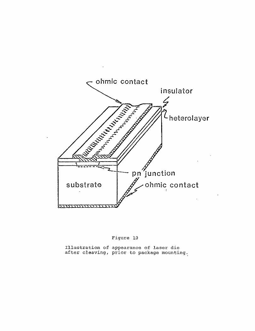
appearance of a laser die after this cleaving procedure is
shown in Figure 10 The laser dice were typically 14 mm
thick x 14 mm wide x 12 mm long
-17shy
WIES WCUTI AS-_GROWN FACET APPEARANCE OF WAFER AFTEARSAING OUTWFR GROWTH
P-N JUNCO
3CROSS SECTION OF WAFER SHOWING DIFFUSED REGIONS
5 FOLLOWING METALLIZATION OF THE JUNCTION SIDE
Figure 8
JDIFFUSION MATERIAL
2 APPEARANCE OF WAFER AFTER EVAPORATION OF DIFFUSION MASK MATERIAL
LAPPED SIDE
4 FOLLOWING WAFER LAPPING TO 250 UM THICKNESS
6 FOLLOWING METALLIZATION OF THE BACK SIDE
Summary of the wafer processing operations used in Pb-salt diode laser fabrication
OR1GINA pAGF 1
OF POOR QUALIT
U
I t
I I4 I I I il 1
S
Igt
i
ohmic contact insulator
heterolayer
pn junction substrate ohmic contact
Figure 10
Illustration of appearance of laser die after cleaving prior to package mounting
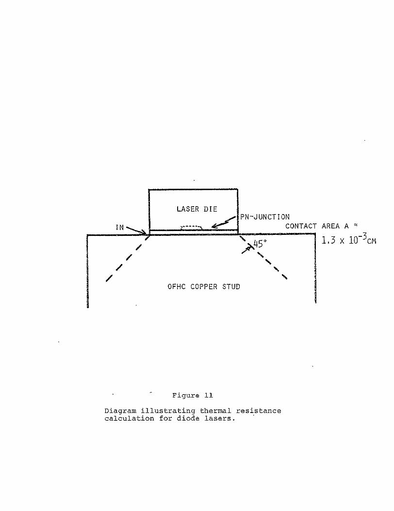
35 Die Mounting in Packages
The laser dice described in the previous section were
mounted with the striped side down on the copper laser stud
This provided for optimal thermal properties since the heat
generated near the shallow junction region was most readily reshy
moved in this manner The thermal resistance properties of this
configuration on the junction side can be obtained by reference
to Figure 11 The total thermal resistance 0T is given by
0T In + 0S
Where 0In is that due to the In metal contact (whose thickness
L is approximately 25 pm) and S is the spreading resistance into
the OFHC copper stud Assuming the thermal conductivity of indium
at 10K is 3 WcmK[15] and the contact area is 13 x 10- 3cm 2
the thermal resistance 0In = 07 KW The spreading resistance
term GS is given by [16]
0S = 2KM
where K is the thermal conductivity of the OFHC copper which is
approximately 5 WcmK and M is the linear dimension of one side
of the area approximately 14 mm Thus
0 ~ 5KW
The total expected thermal resistance of this configuration is
approximately 6 KW In practice this value has been found to
be of the order of 5-10 KW being influenced by thermal resisshy
tance values associated with the stud-to-package contacts as
well as the fact that actual laser dice are mounted at the edge
of the stud This model has also neglected heat removal from
the back side of the laser die but the calculated value is
nevertheless in general agreement with that observed in most
lasers
-18- ORIGINAL PAGE 18
OF POOR QUALITY
LASER DIE
- PN-JUNCTION
I N CONTACT AREA A
oFL45 13 x 10-3CM
OFHC COPPER STUD
Figure 11
Diagram illustrating thermal resistance calculation for diode lasers
I L2
I
Figure 12
SEM photograph of a typical laser die as mounted in the
the heat sink package The photograph was taken by
the NASA Langley Research Center
Dr John Buckley of
fMag = 45X
uOiGll4 pAGE 18)y p014 QUA
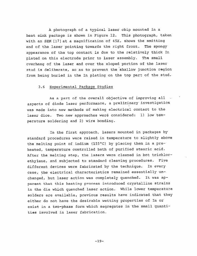
A photograph of a typical laser chip mounted in a
heat sink package is shown in Figure 12 This photograph taken
with an SEM [17] at a magnification of 45X shows the emitting
end of the laser pointing towards the right front The spongy
appearance of the top contact is due to the relatively thick In
plated on this electrode prior to laser assembly The small
overhang of the laser end over the sloped portion of the laser
stud is deliberate so as to prevent the shallow junction region
from being buried in the In plating on the top part of the stud
36 Experimental Package Studies
As a part of the overall objective of improving all
aspects of diode laser performance a preliminary investigation
was made into new methods of making electrical contact to the
laser dice Two new approaches werd considered 1) low temshy
perature soldering and 2) wire bonding
In the first approach lasers mounted in packages by
standard procedures were raised in temperature to slightly above
the melting point of indium (1551C) by placing them in a preshy
heated temperature controlled bath of purified stearic acid
After the melting step the lasers were cleaned in hot trichlorshy
ethylene and subjected to standard cleaving procedures Fiye
different devices were fabricated by the technique In every
case the electrical characteristics remained essentially unshy
changed but laser action was completely quenched It was apshy
parent that this heating process introduced crystalline strains
in the die which quenched laser action While lower temperature
solders are available previous results have indicated that they
either do not have the desirable wetting properties of In or
exist in a two-phase form which segregates in the small quantishy
ties involved in laser fabrication
-19shy
The second approach was a wire-bond technique using
a 0003 diameter gold wire soldered to a shortened top electrode
and pressure-contacted to the laser die It was felt that this
contact would remove the major contact induced strains in the
crystal Pressure was applied with controlled weights on a
piston fixture After several optimization attempts a laser
was successfully fabricated by this technique and delivered to
NASA Langley ResearchCenter (Serial No 6271-3) However the
contact failed during operation and the laser was subsequently
replaced We believe this method has promise but will require
the use of specialized die-bonding equipment and considerable
development time to effect
-20shy
40 LASER EVALUATION
41 Evaluation Methods
411 Dip Stick Testing for Electrical Characterization
The electrical characteristics of the diode lasers
were studied by pltting the I-V curves using a 4-point probe
technique designed to eliminate lead resistance effects The lasers
were mounted in an evacuated dip stick which could be immersed in
a liquid helium reservoir A GeCu infrared detector mounted in
the dipstick made it possible to measure the threshold current
of the laser and obtain an estimate of theoutput power
As an illustration-of the technique a typical
I-V curve of a high performance Pb09555Sn 0445Se CID device is
shown in Figure 3 (This laser was fabricated from crystal G196)
This I-V curve exhibits the slope discontinuity at threshold which
is typical for high performance Pb-salt lasers and indicative of
high internal quantum efficiency [18] The value of the voltage
intercept as shown in Figure 13 is 1045 mV (corresponding to
842 cm- ) in reasonable agreement with the laser threshold freshy-quency of826 cm I observed during subsequent optical testing of
the laser emission More information on the optical charactershy
istics of this device is given in the following section
A photograph of the dipstick test area is shown
in Figure 14 The dipsticks are evacuated after laser mounting
using the cryopumps shown in the figure The test arrangement
is such that 2 lasers can be mounted in each dipstick These
-21shy
__
__________
OF pOOR QUALITYORIG~hIAL PAGE IS
-Fshy
+ _I_ _____ --- -- --- ______ _ _ _ __--
-K - __ -__ __ __ ____-__
- - r I Elctial carceri cs of r----f I F -- ___
- -- -I pa---- -i--- 1K th st aAg t l n ---- =___-_-- - -shy
curv extrapolates ____ _ ono th
t 1 t _ ____
he sjar___
fige ure 13raoats E _ ___ __ __ _c _ -- _ _ x __I
an ____zrEh~zto 104SmV corresponding to _
F- iexpected laser emission of
42 cm nearthreshold -- shy
2D_
________ _________ _- t n~ g t l n o -
t__-- thIta E 1 K _
___ tio urve extapolates ___ 1_v__f 72lfl ___of the - - - - - -=-_
- --- cresodigtoato14m t
II p
IA
I I i I-I
La
e
Tig
ure 14
Laser
Dip
sti k
Testin
g
Area
dipsticks also proved useful for the thermal cycling tests
(described later) since the lasers are located in a vacuum enshy
closure and are therefore protected from moisture condensation
412 Evaluation of Emission Characteristics
The diode lasers fabricated during this program
were studied for a variety of optical performance characteristics
including
Threshold current vs temperature
Output power vs temperature
Spectral distribution vs temperature
Output power vs current
Limited measurements of tuning rate far-field spatial output
distribution and noise were also carried out
4121 Spectral Characteristics
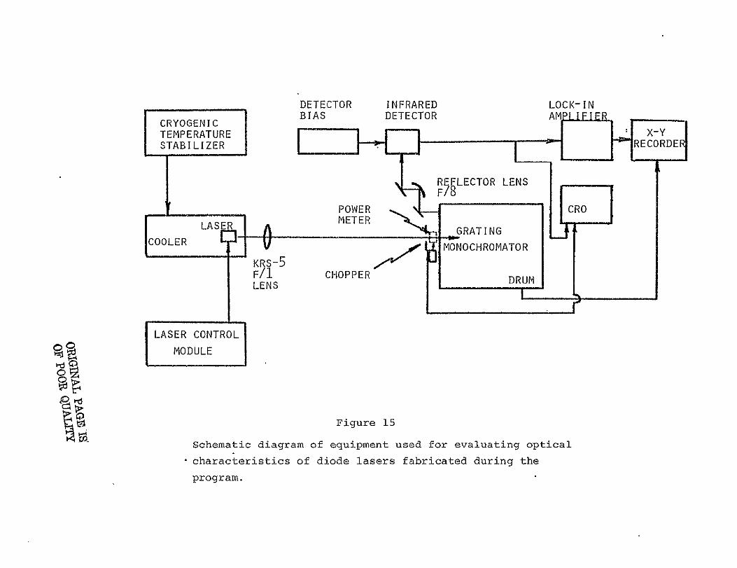
The system used for the majority of
these measurements is diagrammed in Figure 15 The lasers were
mounted in a Laser Analytics Model TCR Stable Temperature Closed
Cycle Refrigerator which allows temperatures to be varied from
10K up to room temperature The collecting element was a corshy
rected fl KRS-5 lens with microadjustment Laser mode charactershy
istics were measured with a 12 meter grating monochromator and
the radiation was detected with a cooled HgCdTe infrared detector
The power output was measured with a 1-cm diameter pyroelectric
detector which could be shifted into the optical path
behind the chopper using a mirror arrangement The power meter
was supplied by the National Bureau of Standards Boulder Colorado
The lasers were powered by a Laser Analytics Model LCM Laser
-22shy
DETECTOR INFRARED LOCK-IN CRYOGENIC BIAS DETECTOR AM
TEMPERATURE X- _ STABILIZER RECORDEI
R LECTOR LENS
POWER CRO METERL RASE A GRATING
COOLE iMONOCHROMATORKRS-5
F1 CHOPPER DRUM LENS
SLASER CONTROL
MODULE
Figure 15
Schematic diagram of equipment used for evaluating optical
characteristics of diode lasers fabricated during the
program
Control Module The output of the system was displayed on both
an oscilloscope and an XY-recorder
As an exaEmple of the spectral measureshy
ments carried out during this program the spectral charactershy
istics observed from laser -7075-12 discussed in the previous section
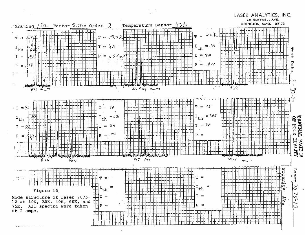
are shown in Figure 16 The threshold frequency of this laser
-is 826 cm in close agreement with that obtained from the zeroshy
current intercept of the extrapolated value of the linear portion
of the I-V characteristics This laser had a maximum CW output
power of 105 mW per end at 127K At 20K the laser ran single
mode with an output power of 088 mW
4122 Spatial Profile Measurement
An Amperex pyroelectric vidicon was
used for preliminary measurements of the spatial distribution
The vidicon sensitivity is such that when the far field pattern
is spread over 50 of its receiving surface it can sense about
50 i-watts of infrared power The laser utilized for-this preshy
liminary experiment was a Pb0 97Sn0 03Se CID device from Laser
Analytics stock The laser was operated in a square wave mode
to provide the required AC signal Results obtained in this
manner are shown in Figure 17 The photograph of the CRT was
taken as the vidicon was slowly moved across the optical path
This mode of operation enhances the display contrast but care
must be taken to interpret this data Adjacent regions of dark
and bright areas correspond to regions of radiation intensity
the bright areas corresponding to the leading edge of travel (the
heating period) and the dark areas corresponding to the trailing
-23shy
LASER ANALYTICS INC 38 HARTWELL AVE
Grating SU Factor )79o Order2 Teperature Sensor -i3 0 LEXINGTON MASS 02173 I ------- bull
- I I shy=
- - = AIthP A
I --- - Ii - ----shy-
I - - (
T
S-------------
1 TIth~- -- --
---
-
-----------
-----shy
---
T 7
T--IIUthh~shy --plusmn - -
-----= I I -A
--- -shy - --shy
------- -------- T- =1_ i--------------T
S T - - = --- uL -7 lt - -------shy
7 1 - - I
9797- -fj 3 ii 1 I
th QFigure 16 th
Mode structure of laser 7075- - I = [ i ------------
--
C12 at 10K 20OK 40K 60K and 75K All spectra were taken - ---------------shyat 2 amps ------r------------shy
Atlt 4
NOR f 1 M Arl-
or n p
Tu44gt
TAW4
4 isVih
iA
0 All
11 4i
I r5 Iamp
+ 4 Ptnira 1
Wri1 ataat10pW 0 agt9 zcar
M4o
)4t 4
44A~ 17 gt~ 444 4
The small bright spot on the right edge (the cooling period)
half of the photograph was due to an imperfection on the vidicon
surface
An important aspect of this experiment
is that concentricrings due to diffraction effects associated
with the refrigerator window nearly mask the laser beam pattern
This result corroborates earlier measurements made by scanning
detector techniques Similar patterns have been reported for
GaAs lasers beamed through external diffraction structures [191
Circumvention of window effects to achieve a reliable measurement
of the spatial pattern would require the use of wedged windows
with anti-relfection coatings Time and cost restraints prevented
the enactment of these remedies hence these measurements were
not further pursued
42 Electrical and Optical Performance Results of Lasers
Delivered to NASA Langley Research Center
A total of nine lasers were delivered to NASA Langley
Research Center during this program Each of the following sections
contains the following information for each laser delivered
(a) I-V characteristics at lOK and 77K
(b) Emission spectra at various temperatures and at
2 amps
(c) Tables summarizing the variation of threshold
current output power (2A) and output frequency
(2A)
-24shy
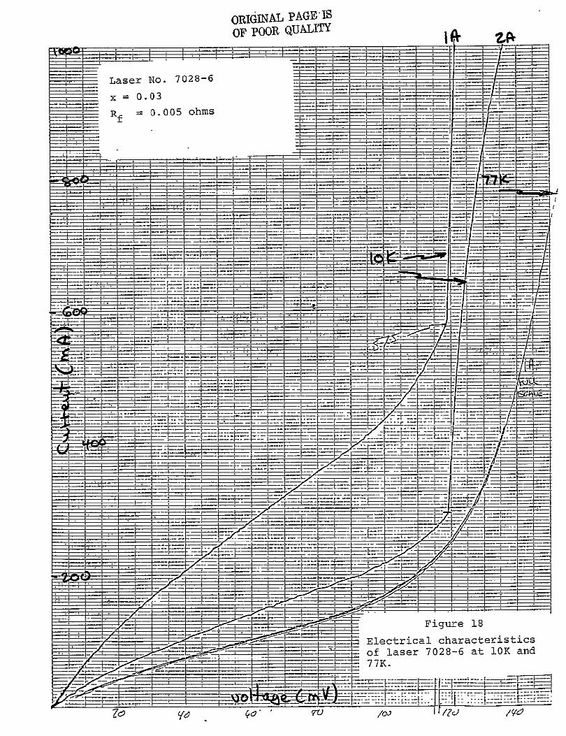
421 Laser No 7028-6
(a) Electrical characteristics (Figure 18)
(b) Spectral data (Figure 19)
(c) Table of Ith Pout and frequency vs
temperature (Table 3)
-25shy
___
oRIBINAL PAGE JS OF POOR QUALITY
7028-6Laser No 0 3x = 0
R = 005 ohms
IFshy
_ _ __ =shy_ __-_ _ _
------ shy---- - - _ -
_t- I -I -shy
__ Ft ---= _ iv___ ~~~__ _ - - __
El crcl hrceristics
- r--r77K _---shy__ _
7Z 77K 7
--
LASER ANAL CS INC 38 HARTWELL AVE
Grating__- - Factor 896 Order I Temperature Sensor 2 5 LEXINGTON MASS 02173 I JU- - JL -I----iI- F F -- =
=I -I-J I -- I-- - - F0 shyt III ILL-II I L j hZth~C C shyt__j _Lplusmn_LI iLWJ - ---I
-IJ miP-I =oq-JjI 4-LLt~z-Utb- - --=oWh- -- L i - IH - --L L iD 6 IPJl Ill shy- P 3 r I-0Hq37i~itIflh1S7L1i41
-~Lwvt-iII 1 1]li~tt LF7 gt_- -- shy1 +4=t I_ _iJL I- -- --
I- I I [IFjIE_II da
I--- III - __~j- ltIII-- I LIwI--J--I---- t III L 1 ~ j t
T tI - J- IhI tI t
ltL- - 11 -LHPltE--_____-__1 1IIIIHIHiA9 plusmn_L plusmn1 -LL plusmn1I-Ph -L - - _ - -1 d-
-iI --- - - -L j I-I
i_ _+I_ +__ Iplusmn_IE_ V_ i-p- ___--_j --_ - -T
FMI-ki i I In ----- I_- + -- j- -H5-l- shy ---- ---- = - --iT- I -I J-1+ II ___riIILL
-i---------- II t ItH --- i tth21 -lit r ]j = IT - ---
- _
-II--I- HL
Figure 19 --- ----- -- Spectral output vs 0 ra- I -_shy
temperature for laser 70286ili - - -- c I -T t-l--r-l
I
Table 3
SUMMARY OF OPTICAL DATA FOR LASER 7028-6
2-Amp2-AMpSingleEndedOutputFrequencySingle-EndedLaser Package CW OutputIthTemperature Range (cm
(K) (mA) Power (mW)
867- 952043962010
961- 978035161020
1049l1060026357740
1150-1155007060060
OPIGINAL PAGE 18
OF PO1R QUALITY
422 Laser No 6271-2
(a) Electrical characteristics (Figure 20)
(b) Spectral data (Figure 21)
(c) Table of Ith Pout and frequency vs
temperature (Table 4)
-26shy
ORIGINALPAE1 OpPBOOR QUALMT
~~ aer No- 6271-2
000 5
H ohm
f R 03
R HI
~~~~~~~~~~~~~~~~~~~~~
shy r--n-rr+amp-
laser
+ 4 Eectrcalharateriticsof-shy
6212t10nd7K
2o 4o61
LASER ANALWIS INC 38 HARTWELL AVE
Grating _ p
Factcr Order Temperature Sensor 3 go LEXINGTON MASS 02173
----- - - - -shy
3[t l [ th--- ---
- i---- tW -t---- - - - - t
T+- P i
--
449
Q -T
i P-H -i-H
t - --
H I------I=
T o( S
- -------------
T -1-I ITT---
D4 it
- = --
- -shy-
1- In
IL I-- E-1T--
igure 21 h tth
temperature
P = Spectral output vs for laser op r t n62712
P =
Table 4
SUMMARY OF OPTICAL DATA FOR LASER 6271-2
2-Amp- output2-AmpSigl-Ende Laser Package Single-Ended Frequency Temperature th CW Output -I
(K) (mA) Power (mW) Range (cm
10 400 0132 727-741
20 490 0105 735-746
40 840 0088 776-788
-60 1540 ~002 851-860
65 1900 -001 875-877
O IJ
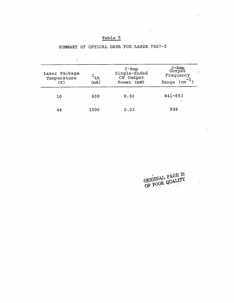
423 Laser No 7067-5
(a) Electrical characteristics (Figure 22)
(b) Spectral data (Figure 23)
(c) Table of Ith Pout and frequency vs
temperature (Table 5)
-27shy
--
--
ORIGINAL PAGE I8 OF POOR QUALIY
Laser No 7067-5
x = 00445
Sf= 00145 ohms
_QCshy
- _---__I
_ __
Figure 22
Electrical characteritc of laser 6067-5 at 10K-and 77K
Syj Zo6 -o )O
- --- ----- - -
LASER ANA4 CS INC HARTWELLAVEL 38X G
5 7-O Order Temperature Sensor _ L NGTON_MASS 0217 3 Grating Factor
-plusmn = o4 kK - S ATELAEKt~ l it tKqi-- - -
Ii4 i--1 - - - I _ - ------- t ---- - -shy
t h I--I- --- - U----
TflTI I4- I Ishy
-- i 1 - ----- --I-IP A
- -th=th th
IL 2 --- -shyt- HP-----
S_ THI
Ii - I -Ht F L-JL - _ ~ t - --th ---shy
] I -plusmn- Iplusmn i 7J +F- 2 I~~
t- igur 2= - - -Jdc-th -I- --
- HutuiSecrl oeatn -S mj 4l_r____- Hii[-ITi
PFigure 231=~~~~- IAi-tWLplusmn - ~i --- ---- Specal output vs operating LIt LWUlterperature for laser 7067-5 - I-iT jFI + - - tI I - -- 1iI ---- --
I HII I I 111111 I ___ L-------iI 11
Table 5
SUMMARY OF OPTICAL DATA FOR LASER 7067-5
2-Amp2-AmpSingleEndedOutputFrequencySingle-EndedLaser Package CW Output1thTemperature shy
(K) (mA) Power (mW) Range (cm I
841-85305060010
909002190048
1S0910GE op QIJMS1
424 Laser No 7067-7
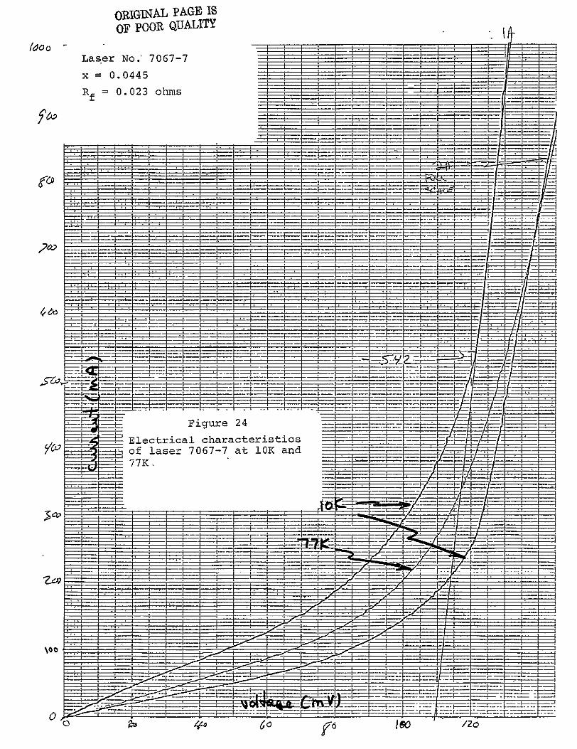
(a) Electrical characteristics (Figure 24)
(b) Spectral data (Figure 25)
(c) Table of Ith Pout and Frequency
vs Temperature (Table 6)
-28shy
OIGINAL PAGE IS
OF POOR QUALITY
Laser No 7067-7
x = 00445
RF- 0023 ohms
- -
d
nFigure 24
_ Electrical characteristics -- of laser 7067-7 at 10K and
It _ - - - -
[6 20dego
LASER ANAYtCS INC 38 HARTWELL AVE
Grating
F actor 7 Order
-- T =
Temperature Sensor
T
lj
- --
LEXINGTON MASS 02173 I
-
th -L- - --- 2t
]th t[j ~ i- 1 -l--H - - - 4 -
_=-h0 - IV
jiP tti--yiplusmn
4 t
th -shy
t 2 gt7J-- --- -
ll- tt ----shy w t jj i I = = - -I-
~- - - ------ --
th
-
p8V
---
_
-
I~L I I =-
I -m-r-shy-L---HT- I=
- --I i
_1-t4 ij_hlIth -
-z
--shy [7
I
-t
- h
F-
- I1 4
1ttt
SS e ta oup t v-pe a i g i __ --I I -
P7 te pe at r fo_ l s 7067 7T= -H+FI I - I I gt 7 lt 1 II ilL I~~L +-I
71771rI- u _ t
T - shy---
------shy
----shy-- 1
Spectral output vs operating temperature for laser 7067-7 -
- plusmn P1 -
i-i -1----i-----I--- E---shy
Table 6
SUMMARY OF OPTICAL DATA FOR LASER 7067-7
2-Amp 2-Amp Output
Laser Package Single-Ended Frequency Temperature th CW -otput
(K) (mA) Power (mW) Range (cm
10 800 0246 834-860
20 860 0175 846-864
36 1480 002 895
ORIGINAL PAGE I1 OF POOR QUALITY
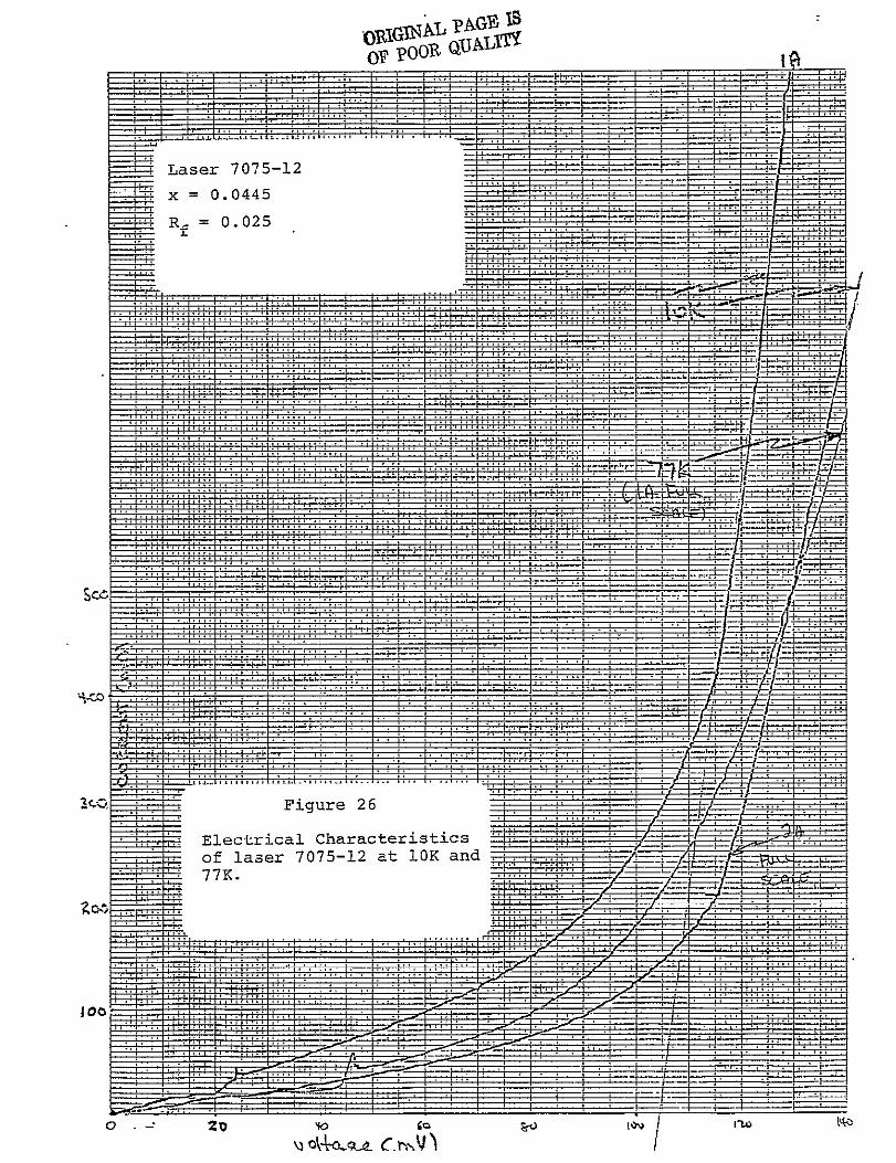
425 Laser No 7075-12
(a) Electrical characteristics (Figure 26)
(b) Spectral data (Figure 27)
(c) Table of Ith Pout and Frequency vs
Temperature (Table 7)
-29shy
OF pouh R
Laser 7075-12
x 00445
Rf 0025
_I 4
I I
26 Figure
CharacteristicsElectrical of laser 7075-12 at
10K and
77K
02D404QA CteAI
LASER ANAI1t S INC - 38 HARTWELL AVE
LEXINGTON MASS 02173pGrating 4 Factor T7B rder r TemperatureSensor Q3amp0
- -t -- aco - - rd - 2v
T T 7 T
- P
~ itIhI th=lg
1rI 2 - th =th=shy
-t -- -- shy Ltemperature-for p-+-- taserW7075-12
Ill(DT
Spectral output vs operatingr -shytemperature for laser 7075-12 P
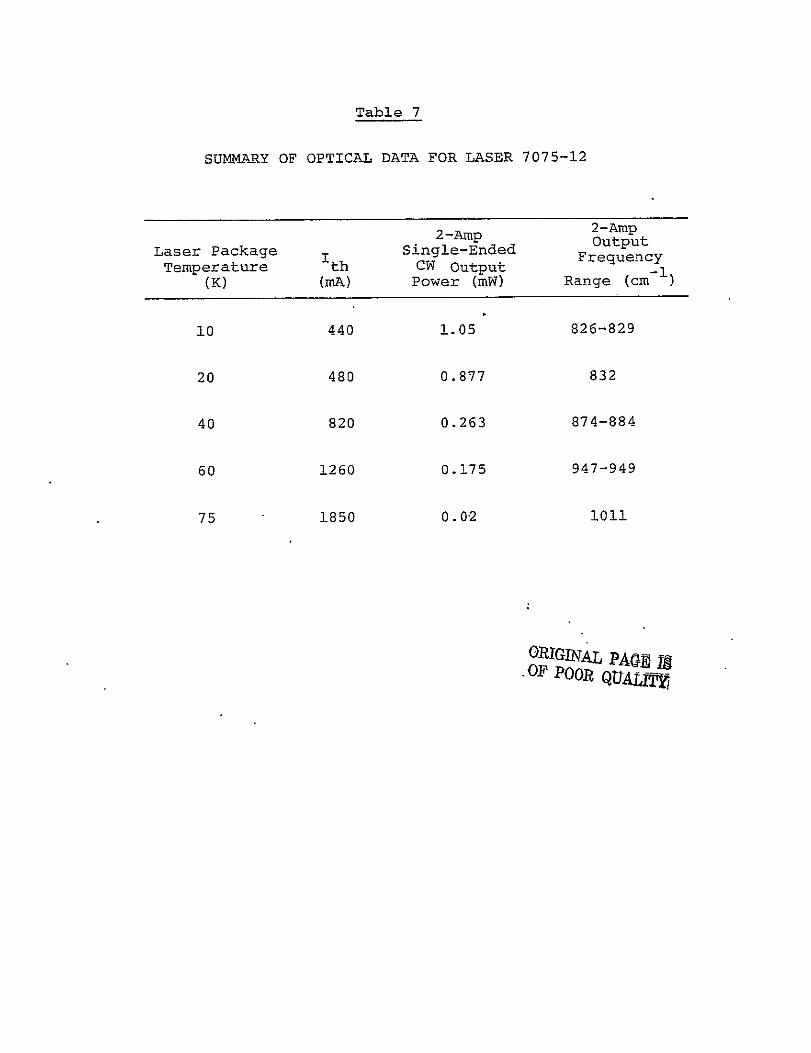
Table 7
SUMMARY OF OPTICAL DATA FOR LASER 7075-12
Laser Package Temperature
(K)
10
20
40
60
75
th (mA)
440
480
820
1260
1850
2-AmpSigl-Ende Single-Ended CW output Power (mW)
105
0877
0263
0175
002
2-AmpOutput Frequency
Range (cm
826-829
832
874-884
947-949
1011
ORIGImNAL PAGE IS OF POOR QuALfij
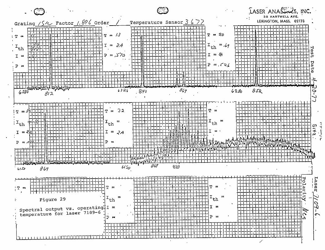
426 Laser No 7109-6
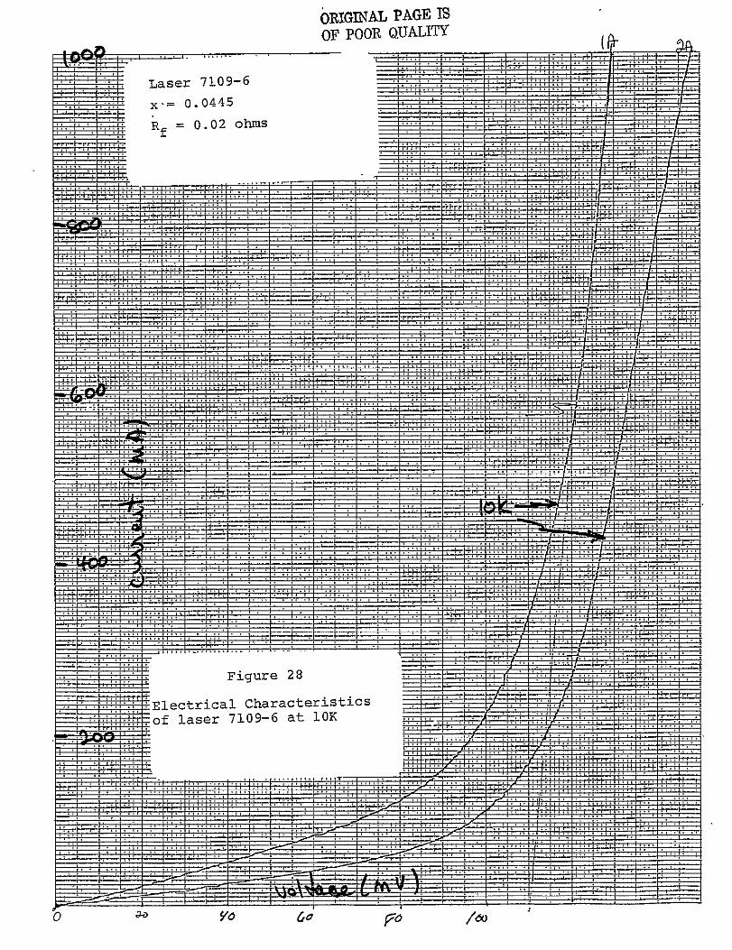
Cal Electrical characteristics (Figure 28)
Cb) Spectral data (Figure 29)
(c) Table of Ith Pout and Frequency vs
Temperature (Table 8)
-30shy
ORIGINAT PAGE IS OF POOR QUJALITY
H-1 Laser 7109-6
i 700445
Hf o02 ohms
v
k
Elecrica
Chractrisics
t
Et
HH
I p
20L
--
D LASER ANAgt25 INC 38 HARTWELL AVE
Grating A Factor4 deg Order Temperature Sensor 3 ( LEXINGTON MASS 02173
T T= S- T =
Ith =QIth = (DmI = I =
6-1
-SP --
-I~II
T T
-T 4-1 1
I - F9
T shy-- IILI ____
- - - - - - - - - s -bull - P- N rtinh I- J ------ t h-shy h -MI I it
=
I Fiur 29SetaOuptV-tprt 4tIl-QwV tepeatr for~ laserI- 7109--- --shyi~ -- -I~~~~~- 3~t sect k
T= I -I- I-- - r -shy -- j-
Table 8
SUMMARY OF OPTICAL DATA FOR LASER 7109-6
2-Amp
Laser Package Temperature
(K)
th (mA)
Sg2-Amp Single-Ended CW Output Power (mW)
output Frequency
-1 Range (cm
10 590 0570 812-864
20 690 0526 852
30 1100 0044 869
32 1900 002 869-890
ORIGINAL PAGE IS OF POOR QUAITY
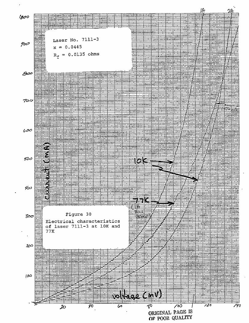
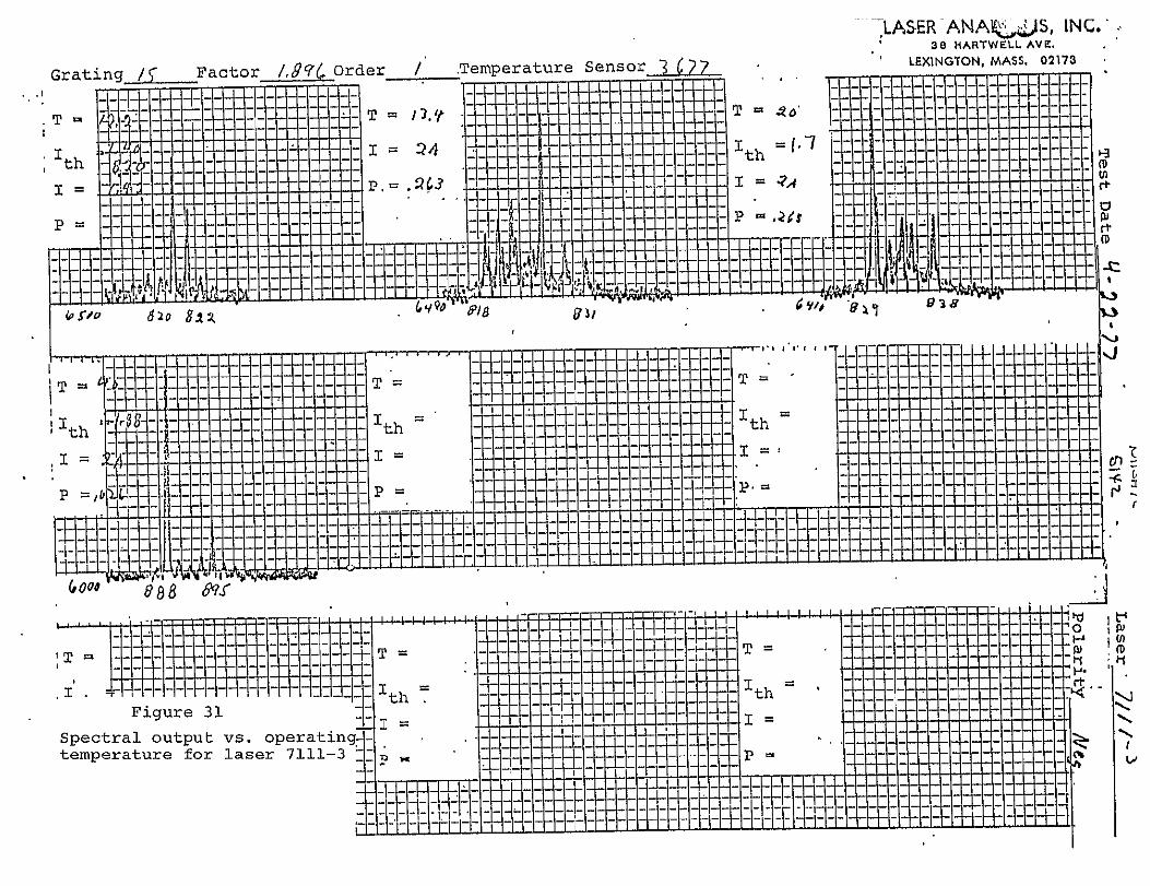
427 Laser No 7111-3
(a) Electrical characteristics (Figure 30)
(b) Spectral data (Figure 31)
(c) Table of Ith Pout and Frequency vs
Temperature (table 9)
-31shy
Laser No 7111-3
=T-= x = 00445
Rf= 00135 ohms
E e
t
i
a
S
~z
ri
E
H rr
r -
I
-
rr
- I
i
P k
70
ORGIA
01
PAGE
0
is
le
II ORGIA PIG lOOR 1
__
---------
-- --
-LASER ANAUS IN(38 HARTWELL AVE
LEXINGTON MASS 02173 Grating _Factor 8c6 Order Temperature SensorjikZZ 1-1 T = T T
th i- (E
P PO -
- -y i=i=D 1 ith
--- - - - - -IT-
tI-- shy
- -- t--I--------
tt~I -t
-- - - -
th---
-1--~~x -- - -r
v -- i-S pu - t
-+) 1 0r--r-
1-empert fo- l
t 88+8 oo+cflamp__
-N
Table 9
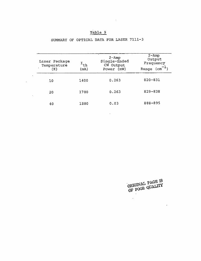
SUMMARY OF OPTICAL DATA FOR LASER 7111-3
2-Amp
Laser Package Temperature(K)
Ith(mA)
2Am Single-EndedCW OutputPower (mW)
Output Frequency-1Range (cm
10 1400 0263 820-831
20 1700 0263 829-838
40 1880 003 888-895
Oolt
428 Laser No 7061-1
(a) Electrical characteristics (Figure 32)
(b) Spectral data (Figure 33)
(c) Table of Ith POut and Frequency vs
Temperature (Table 10)
-32shy
II
ORIGINAL PAGE IS OF POOR QUALITY
_- __=___
xo047 _ _~_________-- -r_~~Rf 0022 ohms -
FEshy
= ~~~~~-- u--- _Lf__f-i_
_
4- L-
IrIshy
~~Figure 32 +kshy
~Electrical characteristics _ __
H of laser -7061-1 at 10K and
- 77K _- _ -shy
-i ----shy I
-- -
-------- -
----- -- - -
i
LASER ANALYTICS 38 HARTWELL AVE
INC
Gtalting (Sp- Factor Order I Temperature Sensor 9ampoR SLWS 20 LEXINGTON MASS 02173
T -L--------
Iiit+L= ---
LL1- -T-0--f - -shyz
Il -----
tt -
-3
H(DAL
- --- hI 1-1 21 i~ --------
IIt
IiK 1 I7-I7 -11 + - [+L3 T I - i
1-i-I--l4 Tth = H 215-i L1I
-Ii----------------P
I L o
T ------ -=--shy
-- - I--------- 0 3
]E -ll -i F- -i--T S e t a ou p t v ng
Itemperature for laser 7061shybull - ---i -- --- -------- _-A4i--------shy7-~~---- 4 --- -----I--
Table 10
SUMMARY OF OPTICAL DATA FOR LASER NO 7061-1
Laser Package Temperature
(K)
10
20
40
60
80
95
th
(mA)
148
158
200
333
680
1520
2-Amp2-AmpSingle-Ended CW Output
Power (mW)
07
07
07
08
06
01
Output Frequency
- IRange (cm 1
770-796
780-800
825-851
894-906
974-1006
1045-1051
429 Laser No 7069-1
(a) Electrical characteristics (Figure 34)
(b) Spectral data (Figure 35)
(c) Table of Ithm Pout and Frequency vs
Temperature (Table 11)
-33shy
_____
----
__
- _I ------
1 _ 7069-r _ Laser
x 0047 1 -- +-shy
f 0027 ohms
t_L___________________-____=Eshy ___
-I -I
_shy- -- H- --~-
7__1_ _ 1L - -- -E
_-_-- ME INshy
_ _
4+- shy_ _- _--
_ - _--
- gt
-- shy 34~~~~Figure
~~Electrical characteristics--i
anoflaser 7069-1 at 10 and-
10
77K
1t0RoeuroT
LASER ANALY ILCS INC 38 HARTWELL AVE
Grating I ) 6f7)Order Teperature Sensor 9 9 LEXINGTON MASS 02173LA-Factor I -- -I -
----- ------ 0 th-n-- yF--- -- - - - - - - --o - - -~ w i-
_th-I = 2t j -v th 3 I= P Ca
iI-I- I - I-------------------]
Th- _z ~I
- -- output iLLL- - - ---peer
VV
----------------------- I ---- 11 x
--shy
0MIshy
th H - - t-ishy
fF- I rplusmn
-11-t -V -I-j -
-----------------
IthH
-1 J-~f T1- Fiur 35 [ 11 ---- Spectral output operatnshy----- vs
-- temperature for laser 7069- --shy
j-4-1- shy
-i
Table i
SUMMARY OF OPTICAL DATA FOR LASER NO 7Q69-
Laser Package
Temperature (K)
10
20
40
60
80
Ith (mA)
122
135
190
332
709
2-AmpSingle-Ended
CW Output Power (mW)
009
009
013
009
-002
2-AmpOutput
-u Range (cm
771-797
782-802
833-849
927-1006
1052-1089
ORIGINAL pAGE IS
OF poop QUALITY
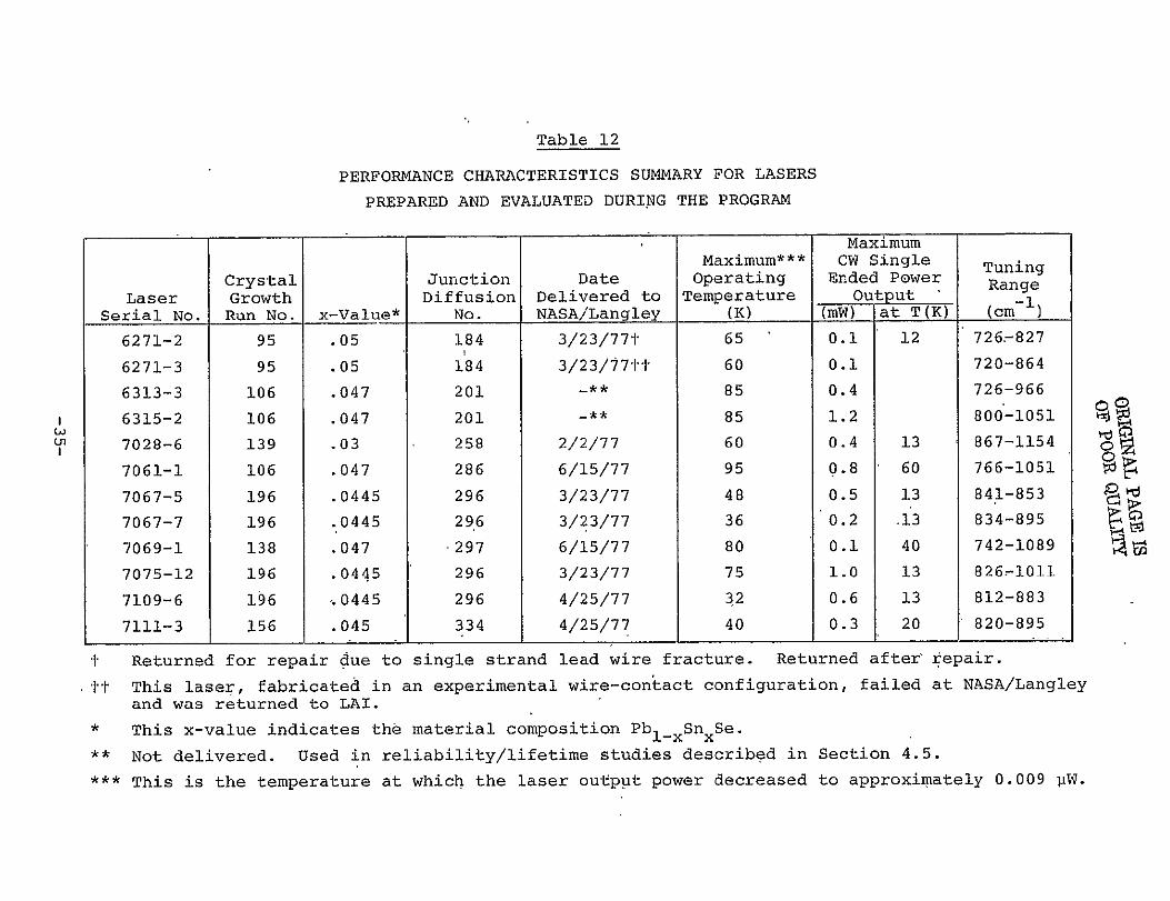
43 Summary and Discussion of Laser Performance Data
Important operating characteristics are summarized in
Table 12 for the lasers whose properties are given in Section 43
above and for two additional devices discussed in the next secshy
tion The following observations are significant
1) Four out of the twelve lasers in Table 12 had CW
operating temperatures above the boiling point of liquid nitrogen
2) Eight out of the twelve- lasers had CW operating
tepperatures in excess of 60K
3) Five of the lasers in Table 12 had CW singleshy
ended power outputs greater than 05 milliwatts
4) Four out of the twelve lasers exibited single mode
CW single-ended power in excess of 05 milliwatts
5) CW operation above liquid nitrogen temperature has
been achieved at wavelengths as long as 1035 pm (the longest
wavelength previously peported for operation of any diode laser
at 77K or above is 96 pm [19] 1
These results represent a substantial improvement in
the state-of-the-art of tunable diode lasers in the 8-15 pm specshy
tral range Previous homojunction lasers -in this range have
generally had maximum operating temperatures below 40K have
never exhibited 77K operation and have consistently produced
maximum CW power outputs of less than 05 milliwatts overall
The CID technology can now be used on a reproducible basis in
both the PbSSe and the PbSnSe systems
The results of the present progtam show that the CID
technology can be used to provide significantly improved pershy
formance on a reproducible basis throughout the 8-15 pm range
-34shy
Table 12
PERFORMANCE CHARACTERISTICS SUMMARY FOR LASERS
PREPARED AND EVALUATED DURING THE PROGRAM
Maximum Maximum CW Single Tuning
Crystal Junction Date Operating Ended Power Range Laser Growth Diffusion Delivered to Temperature Output R -I
x-Value No NASALangley (K) (mW) at T(K) (cmSerial No Run No
6271-2 95 05 184 32377- 65 01 12 726827
6271-3 95 05 184 32377-1-1- 60 01 720-864
726-9666313-3 106 047 201 85 04
1 6315-2 106 047 201 - 85 12 800-1051
7028-6 139 03 258 2277 60 04 13 867-115460 766-1051286 61577 95 08
7061-1 106 047 7067-1 196 0445 296 32377 48 05 13 841-853
7067-7 196 0445 296 32377 36 02 13 834-895
7069-1 138 047 297 61577 80 01 40 742-1089
7075-12 196 0445 296 32377 75 10 13 826r1011
7109-6 196 0445 296 42577 32 06 13 812-883
7111-3 156 045 334 42577 40 03 20 820-895
1 Returned for repair due to single strand lead wire fracture Returned aftertepair
It This laser fabricated in an experimental wire-contact configuration failed at NASALangley
and was returned to LAI
This x-value indicates the material composition Pb1 xSnxSe
Not delivered Used in reliabilitylifetime studies described in Section 45
This is the temperature at which the laser output power decreased to approximately 0009 pW
44 Reliability and Lifetime Studies
A number of failure and degradation mechanisms were
observed and addressed during the course of this program The
following paragraphs discuss these problems and solutions which
have been developed
441 Package Relaxation
During this and other Laser Analytics programs
it was found that a number of lasers exhibited a pronounced inshy
crease in series resistance after a few temperature cyclings beshy
tween room and cryogenic temperatures It was discovered that
the effort resulted from the relaxation of laser package parts
which had been strained at initial assembly This problem was
overcome by straightforward design modifications involving addishy
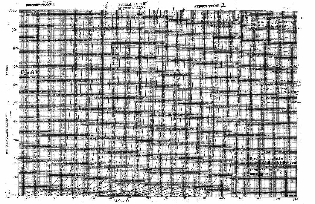
tion of a second set-screw Figure 36 shows a demonstration of
cycling behavior in which a laser was cycled from 300K to 77K
twenty times-with no change in electrical characteristics
442 Crystal Degradation
The term crystal degradation refers to a failure
mode apparently associated with the laser crystal or its deposited
metal layers rather than the package As an example Laser No
7061-1 was stored at room temperature and shipped more than four
months after initial assembly its electrical characteristics at
the time of shipping were given in Figure 32 Figure 37 shows
the electrical characteristics on the date of assembly for comshy
parison It is apparent that during the four-month storage
period the series resistance increased from 6 milliohms to
22 milliohms and the threshold current from 0110 amps to
-
0455 amps
-36shy
OtIGINAL PAGE IS OF POOR QUALITY
As another example Laser No 6313-3 had a
series resistance of 10 milliohms and threshold current of
082 amps at assembly After three months the series resisshy
tance increased to 61 milliohms but the threshold current deshy
creased to 060 amps This threshold reduction dan be related
to a decrease in a pronounced excess current near zero bias
The excess current is thought to be related to surface effects which become less pronounced with time This laser was subseshy
quently destroyed in an attempt to re-seat it in the package
As a third and extreme example Laser No
6315-2 completely failed within a time of one month
443 Low Temperature Storage and Operation
Three high performance CID devices were stored
in liquid nitrogen for varying periods of time Results are
shown in Table 13 The conclusion can be made that negligible
degradation occurs during cryogenic storage
Qualitative observations at our laboratory and
by a number of purchasers of Laser Analytics lasers leads to
the conclusion that high performancePb-salt-lasers do-not deshy
grade for-indefinitely long periods of operation as long as
they are maintained at cryogenic temperature
444 Discussion
Lifetime and reliability problems have in the
past been confused by a combination of effects occurring simulshy
taneously It now seems clear however that a crystal degrashy
dation problem does exist in Pb-salt heterojunction devices
The effect is much more pronounced in MBE and LPE heterojuncshy
tions but is also significant in CID A report on this subject
-37shy
Table 13
LIFETIME STUDIES OF HIGH PERFORMANCE PblxSnxSe CID LASERS
STORED AT LIQUID NITROGEN TEMPERATURE
Rf (42K)Ith (42K)Storage Time (amps) (milliohms)
Laser at 77K After After Serial No x-Value (Months) Initial Storage Initial Storage Comments
76315-1 0047 3 046 046 80 80
7068-1 0030 3 046 052 90 110 Increased Ith related to increased excess current
7068-2 0030 2 038 036 170 170 Decreased Ith related to decreased excess current
-with recommendation for action has been submitted to NASA by
Laser Analytics [21]
Since the effect is most pronounced with heteroshy
junctions it is likely to be associated with lattice mismatching
Thus one solution may be to further perfect the quaternary
growth procedures discussed previously Alternatively an opshy
timization of the degree of lattice mismatch may be possible
the tradeoff would be the height of the heterobarrier
Finally if a short range solution should not
be feasible a practical fall-back position is to maintain the
lasers at or below liquid nitrogen temperature continually
-39shy
-4-4-4
+ -r r4 t
tli1m fi
V4M
C ti LIM fIN Tl ZfK
-----------
ORIGINAL PAGE IS OF POOR QUALITY -
9 ---0 -- --- 1 - -F- - - -- -shy
-oo - - --- I 1 - - + - _ _- -+ = a--- - -- = - i--t--- -t - k -_ + _
t i - I -
r - t =
1 -
- r--+ - EZ--- r - - ----I - - - --- F h--zshy
Io- shy
r - 7_- 1 at- t -
-- - I t J ti i i [V]
time of fabricat ion
--- - -
--- --
50 CONCLUSIONS AND RECOMMENDATIONS FOR FURTHER WORK
51 Results
The central result of this program is that theCID
Technique has been successfully applied to produce single heteroshy
junction Pb-salt diode lasers with significantly improved pershy
formance Single-modeCW power outputs as high as -05 milliwatts
have been achieved at an operating temperature of 20K and CW
operationabove 77K has been obtained for wavelengths as long
as 1036 pm Ten laserswere delivered to NASA under the conshy
tract of which two operated CW above 77K and seven above 60K
Two additional lasers operating above 77K were fabricated and
used in reliabilitylifetime studies These results represent
a significant advance over earlier homojunction methods which
typically result in maximum attainable single mode CW power
nilliwatts and maximum operating temperaturesmuch less than 01
less than 40K
Contact degradation manifested by increased series reshy
sistance and consequentialperformance degradation was noted
and explored Significant progress was made in definingthe -
effect Astop-gap solution to degradation problemswas found
to be storage at liquid nitrogen temperature
5-2 Recommendations
Continued work with CID structures should include a
systematic study of both pn-junction and heterobarrier diffusion
properties At the present time the carrier confinement width
is only qualitatively known or controllable An improved strucshy
ture with confinement widths of less than 1 pm may result in
very substantial improvements in both output power and operating
temperature In addition to an improved confinement structure
control of junction and barrier depths will allow optimization
of junction depth with regard to thermal properties Pn-junction
-40shy
diffusion depths can be measured by angle-lapping and probing
techniques Heterobarrier depths require an EMB system for efshy
fective measurement
Investigations into reducing the barrier height differshy
entialby using a more closely matched x-value in the CID difshy
fusion source may reduce lattice mismatch problems andimprove
room temperature storage properties Alternatively further
research into quaternary compound formation may result in zero
lattice mismatch
The sublimed binary experiment indicated that crystal
growth procedures are not optimum and that new purification
techniques may result in greatly improved crystal quality
It is strongly recommended that a systematic investishy
gation into reliability and lifetime questions be immediately
instituted and vigorously pursued
Noise properties of diode lasers areimperfectly
characterized and not well understood A systematic investigashy
tion of noise and instabilities in tunable diode lasers would be
of considerable value
Preliminary investigations of liquid phase epitaxy
(LPE) have indicated high performance devices can be obtained
While reliability and yield problems presently dominate this
technology future efforts aimed at obtaining a better undershy
standing of these phenomena are indicated For the long range
double heterostructures are expected to result in devices subshy
stantially better than single heterostructures
The above recommendations are believed to be of parshy
ticular importance as a result of the findings of the present
program Other important areas to pursue include 1) improvement
ORIGJINA pAGFI 1S - 4O QUAUW
of contact metallization procedures 2) new packaging techniques
3) stripe-width optimization 4) development of anti-reflection
coatings and 5) investigation of controlled doping by foreign
impurities
-42shy
60 REFERENCES
1 KJ Linden KW Nill and JF Butler IEEE Journal of
Quantum Electronics August 1977 (to be published)
2 AR Calawa TC Harman M Finn and P Youtz Trans AIME
242 374 (1968)
3 TC Harman and Ivars Melngailis Applied Solid State
Science R Wolfe editor Academic Press New York
(1974)
4 TC Harman and JP McVittie Jour Electronic Materials
3 843 (1974)
5 SH Groves KW Nill and AJ Strauss Appl Phys Lett
25 331 (197-4)
6 JN Walpole AR Calawa TC Harman and SH Groves
Appl Phys Lett 2-8 552 (1976)
7 JN Walpole private communication
8 KW Nill and SH Groves private communication
9 RW Broderson JN Walpole and AR Calawa J Appi
Phys 41 1484 (1970)
10 S Yamamoto Science Reports Tohoku University 40 11 (1956)
11 M Neuberger IV-VI Ternary Semiconducting Compound Data
Tables EPIC-S16 p- 22 March (1976)
12 MH Pilkuhn and H Rupprecht J Appl Phys 38 5 (1967)
-43shy
13 CA Kennedy and KJ Linden J Appl Phys 41 252 (1970)
14 L Laugier J Cadoz M Faure and M Moulin J Crystal
Growth 21 235 (1974)
15 R Radebaugh Rev Sci Instr 48 93 (1977)
16 R Scapple Sol State Tech 74 April (1974)
17 SEM photos were taken by Dr John Buckley of the NASA
Langley Research Center
18 JN Walpole AR Calawa RW Ralston TC Harman and
JP McVittie Appl Phys Lett 23 620 (1973)
19 i Hayashi Appl Phys 5 25 (1974)
20 ED Hinkley RTKu KW Nill and JF Butler Appl
Optics 15 1653 (1976)
21 Laser Analytics -ReportLAI 77-2-9 February 15 1977
-44shy
APPENDIX A
A portion of the results of this program was included in the
following article
Single Heterostructure Lasers of PbS lxSex and Pbl1 x
Sn Se With Wide Tunabilityx
K J Linden K W Nil and J F Butler
Journal of Quantum Electronics (to be published in
August 1977)
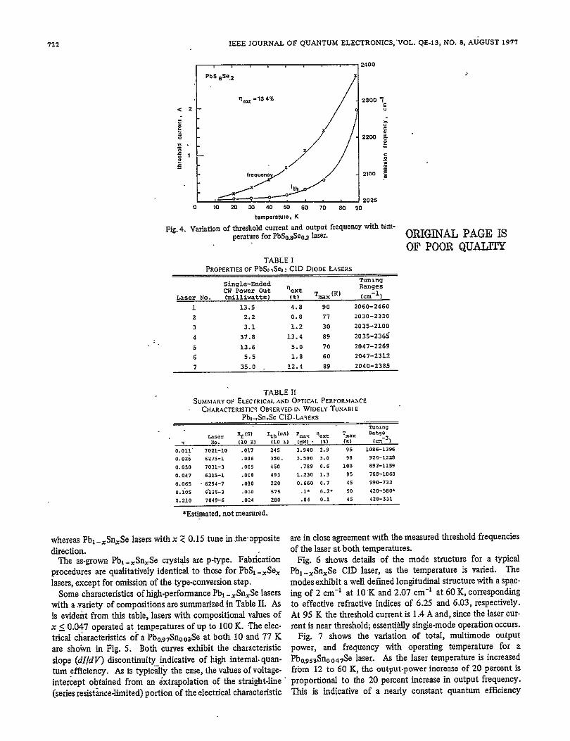
720 IEEE JOURNAL OF QUANTUM ELECTRONICS VOL QE-13 NO 8 AUGUST 1977
Single Heterostructure Lasers of PbSl-xSex and Pbl-xSnxSe with Wide Tunability
K J LINDEN MEMBER IEEE K WNILL MEMBER IEEE AND J F BUTLER SENIOR MEMBER IEEE
Abstrcr-Single-heterostrueture diode lasers formed by composi-tional interdiffusion in PbS_xSe and Pb1 xSnxSe and by liquidshyphase-epitaxy (LPE) in Pbl SnSe show performance characteristics _ significantly better than those observed in conventional homostmeture lasers Higher operating temperatures were obtained for all composi-
tions with CW operation above 77 K being achieved for compositions corresponding to wavelengths from 41 to 127 Arm Single-ended CW powers as high as 70 oW corresponding to lext = 44 percent were ob-served in PbSi _Se devices
I INTRODUCTION
T HE TERNARY Pb-salt semiconductors Pb1-CdS PbS-Se- and Pb-xSnSe provide tunable diode lasers0
throughout the infrared region of 3-30 pm These lasers are finding a growing use in spectroscopy-related applications where they provide measurement capability far beyond that of conventional instruments In spectral absorption studies for
example they allow measurements with a resolution better than 10 4 -cm which is many orders of magnitude better than conventional instruments [1] For monitoring air pollutants and other trace gases they offer the prospect of long-path measurements sensitivity in the sub-ppb range and the ability to discriminate between interfering species to a degree com-pletely unattainable by conventional techniques [2] Further
interest has been generated by their use as local oscillators in heterodyne -receivers for infrared astronomy [3] stratospheric ozone monitoring [4] and other uses
Widespread utilization of Pb-salt lasers has in the past been hindered by their very low operating temperatures typically 30 K or less Improvements in fabrication techniques to be de- scribed in this paper substantially increase operating tempera-tures and in particular make operation of these lasers above 77 K a reality for the spectral range from 4 pm to at least 127 pm These higher operating temperatures both extend the temperature tuning range for laser spectrometry applica-tions and greatly simplify the cooling apparatus requirements in fixed-wavelength monitoring instruments The improved performance results from the development of new techniques to form single-heterostructure diode lasers of PbSi-xSeX and Pb -SnSe Most of the results are based on the use of a new technique compositional Interdiffusion (CID) although pre-limmary results for liquid-phase-epitaxy (LPE) heterostructures in lib -SnSe are also reported
Manuscript received March 22 1977 Portions of this work were supshyported by NASA-LangleyResearch Center Hampton VA
The authors ae with Laser Analytics Inc Lexington MA 02173
100
90o PbSe
8o region of SnSe outshydiffuson I
I
b
- Pb955Sn co45u
gt20
o SnSe
2 4 6 8 10 12 14
ditnce below surface (ion)
Fig 1 Compositional interdiffusion (CID) effect as determined by electron-beam meroprobe analysis of PbogssSno04 SSe dafer anshy-nealed with Pbog9SnooiSe source at 600C for 65 hours
II HETEROSTRUCTURE FORMATION BY CID
-CID is a technique that involves the creation of a single hetshyerostructure in any pseudobinary compound in whichthevapor pressures of the binary constituents are different [5] In the case of Pb-salt chalcogenides the vapor pressure of the low band-gap binary constituent is greater than that of the high band-gap binary constituent [6] [7] Thus by annealing a crystal of Pb-xSnSe with x = xi in a closed ampoule toshygether with a source of composition x = x2 such that x gt x 2
the surface composition of the crystal will change to-that of x The depth ofthe composition change is dependent on the time and temperature of the anneal Ajunction may be formed either during the interdiffusion or as a separate operation Typically a CID of 6 hours at 600degC results in a depth of 5 um The junction depth can then be tailored to any desired value by a subsequent diffusion The CID effect has been exshyperimentally verified by electron microprobe analysis as illusshytrated in Fig 1 [8] -
Single heterostructures were formed by CID in p-type crysshytals Stripe geomefiy p-n junctions were subsequently proshyduced by diffusion through a diffusion mask forming 50-prfi wide stripes Control of stoichiometry was used for carriershyconcentration control and p-n junction formation Ohmic conshytacts were made with Au and In on the p- and n-sides respecshytively The laser chips were formed by cleaving along [100]
tEBM analysis was carried out by A J Strauss and MC Finn of the MIT Lincoln Laboratory
Copyrightcopy1977 by The Institute of Electrical and Electronics Engineers Inc Printed in USA Annals No 708QE035
- -
721 LINDEN er at SINGLE HETEROSTRUCTURE LASERS
Fig 2 Pb-salt diode laser package designed to provide heat sinking on
both sides of laser chip
surfaces to final dimensions With typically -400 pmn between2 end-faces The lasers were mounted in packages designedfor efficient heat removal from both sides of the chips A laser mounted in its -package is illustrated in Fig 2 Laser tuning data indicate that thermal resistances -of lasers mounted in these packages is of the order of 1KW at 12 K
III PbS1 -Se DIODE LASERS FORMED BY CID
CID diode lasers have been fabricated from PbS_Se throughout the entire compositional range The as-grown crys-
tals were n-type and were type-converted by a lugh-temperature
anneal in the presence of a Sl-Se-rich source ingot The crystals were then heated m the presence of a Pb-rich diffusion
source to simultaneously produce a CID heterostructure and a p-n junction
Lasers fabricated from these crystals generally exhibited high quantum efficiencies with low threshold currents and low se-ries resistance values The electrical I-V characteristics of a high-performance CID PbSosSeo laser are shown in Fig 3 A pronounced slope discontinuity is exhibited at threshold im-plying high internal quantum efficiency [9] This behavior is observed in all our heterostructure Pb-salt lasers For this laser
the series resistance is less than 5 ma The variation in thresh-old current and emission frequency with temperature of a typ-ical PbSo8Se0 2 CID diode laser is shown in Fig 4 Table I summarizes the operating characteristics of this device and six others fabricated from the same crystal The series resistances
T= 0K
Cl
100 200 300
voltage mv
Fig 3 Electrical characteristics of PbSo8Se02 diode laser at 10 K Deshymm longvice active area is 50 gn wide by 05
of these devices varied from 5 to 15 m 2 and threshold currents from 45 to 130 mA
The maximum operating temperature we have observed for a PbS_Se CID laser operating CW at 2 A is 130 K achieved with PbS0o 3Seo97 This device exhibited a CW single-ended power output of 70 mW corresponding to rfext = 44 percent
IV Pb1 -SnSe DIODE LASERS FABRICATED BY CID
Pb1 _Sox e single-heterostructure CID lasers have Been fabshyricated with x ranging from zero to 021 The latter composishytion is beyond that of the well-known energy-band cross-over [10] Pb1 -SnSe lasers with compositions in this range tune to lower frequencies with increasing temperature
722 IEEE JOURNAL OF QUANTUM ELECTRONICS VOL QE-13 NO 8 AUGUST 1977
2400
PbS 8e2
next 134 2300 2lt2
2200
2100frequec
th - _1 2025
0 10 20 20 40 50 60 70 80 90
temperatue K
Fig 4 Variation of threshold current and output frequency with temshy
perature for PbSosSeo2 laser ORIGINAL PAGE IS OF POOR QUALITY
TABLE I PROPERTIES OF PbSo Seo CID DIODE LASERS
TuningSingle-Ended RangesnextCW Power OutLaser No (milliwatts) () max(K) (cm 1)
1 135 48 90 2060-2460
2 22 08 77 2030-2330
3 31 12 30 2035-2100
4 378 134 89 2035-2365
5 136 50 70 2047-2269
6 55 18 60 2047-2312
7 350 124 89 2040-2385
TABLE II SUMMARY OF ELECTRICAL AND OPTICAl PERFORMANCE
CHARACTERISTICS OBSERVED IN WIDELY TuNABI E
Pb-SnSe CID-LASERS Tuning
exP T
max RangeLaser Rf(O) IthI
) P
3 No (10 Xl (10 L) (W) - I) (I (cn )
0011 7021-10 017 245 3940 29 95 1086-1396
0026 6275-1 006 350 3500 30 98 926-1228
0030 7031-3 005 450 789 06 100 892-1159
0047 6315-1 008 493 1230 13 95 768-1063
0065 - 6294-7 010 220 0660 07 45 590-733
01Os 6135-3 030 575 - 02- 50 420-580shy
7049-6 024 280 04 01 45 428-3310210
Estimated not measured
whereas Pb -SnSe lasers withx Z 015 tune inthe-opposite are in close agreement with the measured threshold frequencies1
of the laser at both temperaturesdirection The as-grown Pb1 xSnrSe crystals are p-type Fabrication Fig 6 shows details of the mode structure for a typical
procedures are qualitatively identical to those for PbS1 _Sex Pb1 _SaxSe CID laser as the temperature is varied The
lasers except for omission of the type-conversion step modes exhibit a well defined longitudinal structure with a spacshy--Some characteristics of high-performance Pb -xSnSe lasers ing of 2 cm 1 at 10K and 207 cm at 60 K corresponding
with a variety of compositions are summarized in Table II As to effective refractive indices of 625 and 603 respectively
is evident from this table lasers with compositional values of At 95 K the threshold current is 14 A and since the laser curshy
x lt 0047 operated at temperatures of up to 100 K The elec- rent is near threshold essentially single-mode operation occurs
trical characteristics of a Pbo9 1Sno0 3Se at both 10 and 77 K Fig 7 shows the variation of total multimde output
are shoWn in Fig 5 Both curves exhibit the characteristic power and frequency with operating temperature for a
slope (dIdV) discontinuity indicative of high internal quan- Pbo 9s3Sno0o41Se laser As the laser temperature is increased
turm efficiency As is typically the case the values of voltage- from 12 to 60 K the output-power increase of 20 percent is
intercept obtained from an ixtrapolation of the straight-line proportional to the 20 percent increase in output frequency quantum efficiency(series resistiuce-limited) portion of the electrical characteristic This is indicative of a nearly constant
723 LINDEN et al SINGLE HETEROSTRUCTURE LASERS
2
10K C 177K
0
0 100 200
voltage (mv)
Fig 5 Electrical I-V characteristics- of Pb0 9Sn0o03 Se laser at 10 and 77 K Extrapolated voltage intercept values correspond closely to the measured threshold frequency values at these temperatures
-fT 10K
-782 all c1
1 920 oaf
1
11067 cm 95
Frequency -
Fig 6 Mode structure of Pboss3Snouo4Se liser at 10 60 and 95 K All spectra were taken at2-A laser current
within this entire operating temperature region The range of laser tunability extends over 300 cm - from 1302 to 937pym with the region from 102 to 937 pm occurring-above liquid nitrogen temperature
V Pb 1 _SnSe LASERS FORMED BY LPE
Thissection presents the first reported results obtained from heterostructure lasers of Pb -SnxSe grown by LPE The epshyitaxial layers ofPbl xSnxSe were depositedon [100]oriented vapor grown Pbo93 4Sno066 Se substrates and stripe-geometry lasers were formed by diffusion masking techniques Perfor-mance characteristics of four lasers with operating temperatures above liquid nitrogen are summarized in Table III Electrical characteristics-of these devices also exhibited slope discontinu-ities indicative of high internal quantum efficiencies A plot of shytotal multimode CW output power per end (at 2-A operating current) together with laser frequency versus T is shown in Fig 8- In this case a 90 percent increase in output power between
2 Details will be described in a subsequent paper
12 and 60 K is observed corresponding to an increase in-exter nal quantum efficiency from 04 percent at 12 K to 06 pershy-cent at 60 K
The laser- shown in Fig 8 has a tuning range of 319 cm- covering the range from 1107 pm at 90 K to 1712 pim at 12 K This laser produces the longest reported diode laser wavelength (127 pm) atliquid nitrogen temperature
VI CONCLUSION
Single-heterostructure diode lasers of PbS _Se and Pb-xSnSe exhibit marked increases in operating temperature over previous homojunction lasers in these materials In par ticular operating temperatures of liquid nitrogen or above have been achieved at wavelengths as long as 127 pm In all wavelength regions large increases in temperature-tuning range result from higher attainable operating temperature
These higher operating temperatures greatly increase the useshyffulness of Pb-salt lasers in high-resolution spectrometry as a reshysult of their corresponding increased tuning range Perhaps of
greater potential significance relatively simple cooling techshy
724 IEEEJOURNAL OF QUANTUM ELECTRONICS VOL QE-13 NO 8 AUGUST 1977
125 - 1100
Power
100 1000
075 9007 vE
050 Frequency 800
o 025 700
0
10 50 100
Temperature (K)
Fig 7 Single-ended output power and frequency as afunction of opershyating temperature for Pbog 53 Sno4-7Se CID diode laser operating at 2 A
TABLE III SUMMARY OF PERFORMANCE CHARACTERISTICS OF PbO931SI10o66Se
STRIPE GEOMETRY LASERS FABRICATED BY LPE - llxiau c~Tunt ng
R almum CW Range)Laser f Output Power (KI (cmNo (ohms) Per End (nw) TMax I
6309-5 0012 053 90 584-903 6309-2 0006 026 80 605-921
6289-5 0003 - 002 85 626-867
6289-6 0070 2G as 623-854
OFJ 6
SI 9005
4s 800
bull a- oo=3-700 t
~frequency 2 - 600
0
10 50 100
temperature K
Fig 8 Single-ended output power and frequency as a function of opershyating temperature for Pbo9 34 Sno0 6 6Se LPE diode laser Laser curshyrent is 2 A
niques available at liquid nitrogen temperatures and above will Infrared heterodyne spectroscopy of astronomical and laborashynow make it practical to consider a variety of advanced tun- tory sources at 85 pm NASA Goddard Space Flight Center
document X0691-74-237 Aug 1974 able diode laser instruments for trace-gas monitoring and other [4] M A Frerking and D JMuehlner Infrared heterodyne specshy
applications troscopy of atmospheric ozone Appl Opt vol 16 pp 526shy528 1977
REFERENCES [S] E D Hinkley R T Ku K W Nilland J F Butler Long-path monitonng Advanced instrumentation with a tunable diode lashy
[1] E D Hinkley K W Nil and F A Blum Infrared spectroscopy serAppl Optvol 15pp 1653-1659 1976 with tunable lasers in Topics in Applied Physics vol 2 H [6] D A Northrup Vaporization in the PbTe-SnTe system J Walther Ed New York NY Springer-Verlag 1976 chapter 2 Electrochem Soc vol 118 pp 1365-1370 1971
[2] ED Hinkley andP L Kelley Detection of air pollutants with (7] C Hirayama Y Ichikawa and A M DeRoo Vapor pressures of tunable diode lasers Science vol 171 p 635 1971 tin selenide and tin telluride JPhys Chem vol 67pp 1039shy
[31 M Mumma T Kostiuk S Cohen D Buhl and P C VonThuna 1042 1963
725 LINDEN et al SINGLE HETEROSTRUCTURE LASERS
[8] K J Linden J F Butlerand K W N11 Single heterostiucture - P McVitte Single heterojunction Pb1 -xSnxTe diode lasers
tunable diode lasers formed by compositional mtexdiffusion in Appl PhysLet vol 23 pp 620-622 1973 IEEE Int Electron Devices Meeting-Tech Dig 1976 pp 132- [10] T C Harnan A R Calawa 1 Melngailis and J 0 Dimmock
135 Temperature and compositional dependence of laser emission in
[9) J N Walpole A R Calawa R W Ralston T C Herman and Pb SnxSeAppL Phys Lett vol 14 pp 333-334 1969
ORIGINAL PAGE IS OF POOR QUALUT

FINAL REPORT
ADVANCED DEVELOPMENT OF Ph-SALT
SEMICONDUCTOR LASERS FOR THE
80 TO 150 MICROMETER
SPECTRAL REGION
NASA Contractor Report 145259
Contract NASl-14448
Submitted to
National Aeronautics and Space Administration Langley Research Center Hampton Virginia 23665
Dr Frank Allario Contract Monitor
by
Laser Analytics Inc 38 Hartwell Avenue
Lexington Massachusetts 02173
---
TABLE OF CONTENTS
10 INTRODUCTION
11 Program Objectives
12 General Approach
13 Summary of Results
20 CRYSTAL GROWTH AND MATERIALS PREPARATION
21 Crystal Growth-Methods
211 General Description
212 Procedures
213 Growth Furnace Characteristics
214 Residual Gas Pressure Effects
215 Purification by Binary Sublimation
216 Summary of Crystal Growth Runs
22 Compositional Interdiffusion (CID)
221 Background
222 Techniques Employed
223 Experimental Verification of the CID Process
224 Lattice Matching Experiment
23 Pn Junction Diffusion
30 DEVICE FABRICATION
ORIGAL A OF POOR QUALM31 Crystal Processing
32 Stripe Formation and Diffusion
33 Metallization
34 End-Face Cleaving
35 Chip Mounting in Packages
36 Experimental Package Study
40 LASER EVALUATION
41 Evaluation Methods
411 Dip-stick testing for Electrical Characterization
412 Evaluation of Emission Characteristics
4121 Spectral Characteristics
4122 Spatial Profile Measurements
42 Electrical and Optical Performance Results of Lasers
Delivered to NASA Langley Research Center
421 Laser No 7028-6
422 Laser No 6271-2
423 Laser No 7067-5
424 Laser No 7067-7
425 Laser No 7075-12
426 Laser No 7109-6
427 Laser No 7111-3
428 Laser No 7061-1
429 Laser No 7069-1
43 Summary and Discussion of Laser Performance Data
44 Reliability and Lifetime Studies
441 Package Relaxation
442 Crystal Degradation
443 Low Temperature Storage and Operation
444 Discussion
50 RECOMMENDATIONS FOR FURTHER WORK
51 Results
52 Recommendations
-iishy
60 REFERENCES
APPENDIX A Single Heterostructure Lasers of PbSlxSex and
Pb xSnxSe With Wide Tunability K J Linden
K W Nil and J F Butler
-1ii1shy
10 INTRODUCTION
11 Program Objectives
The objective of this program was to develop the techshy
nology for producing Pb-salt diode lasers for the 8-15 pm spectral
region suitable for use as local oscillators in a passive Laser
Heterodyne Spectrometer (LHS) Consideration was given to long
range NASA plans for the utilization of the passive LHS in a
space shuttle environment Specific goals included 1) achievement
of a power output of 05 milliwatts per mode 2) detailed evaluashy
tion of laser characteristics and 3) delivery of lasers to NASA
Langley Research Center for evaluation
12 General Approach
The general approach was to further develop the method
of Compositional Interdiffusion (CID) recently reported by Laser
Analytics Inc and used successfully at shorter wavelength [11
This technology has been shown to provide an effective and reshy
producible method of producing a single-heterostructure (SH) diode
of either the heterojunction or single-sided configuration The
program included refinements in crystal growth and materials proshy
cessing techniques investigations into new fabrication methods
and a study of temperature cycling and lifetime problems
13 Summary of Results
Performance specifications were exceeded in several
devices with single-ended CW power outputs as high as 088 millishy
watts in a mode being achieved The majority of the CID lasers
fabricated during the program had CW operating temperatures of
over 60K 30 of them operated CW above the boiling temperature
-1shy
of liquid nitrogen CW operation above liquid nitrogen temperashy
ture was possible for wavelengths as long as 103 pm Operation
at 77K is significant with respect to space shuttle operations
since it allows considerable simplification of cooling methods
In addition to performance laser improvements the program inshy
cluded 1) an experimental verification of the CID effect which
resulted in valuable new insight into the CID process 2) a
study of reliability and failure modes and 3) investigations into
several specific new areas of materials processing and device
fabrication
The results of this program represent a substantial
improvement in the state-of-the-art of tunable diode lasers in
the 8-15 pm spectral range Previous homojunction lasers in
this spectral range have generally had maximum operating temperashy
tures below 40K have never exhibited 77K operation and have
consistently produced maximum CW power outputs of less than 05
milliwatts overall The CID technology can now be used on a
reproducible basis in both the PbSSe and the PbSnSe systems
-2shy
20 CRYSTAL GROWTH AND MATERIALS PREPARATION
21 Crystal Growth Methods
211 General Description
The standard crystal growth method used at Laser
Analytics (and thatused for crystals grown for this program)
is a closed tube ingot nucleation method whereby an evacuated and
sealed quartz ampoule containing a coarse crush of the desired
material composition is placed in a tubular furnace which has been
previously profiled to have the proper temperature distribution
for optimum crystal growth During the growth period (which
typically requires 3 to 4 days) sublimation vapor transport and
recrystallization results in the growth of a number of crystals
at various positions in the capsule usually directly on some of
the source crush These crystals are generally characterized by
planar facets (usually [1001-oriented) which are utilized in device
fabrication Such material has in the past been found to be of
high crystallographic quality with the as-grown facets exhibiting
dislocation densities in the 104 cm- 2 range prior to handling
212 Procedures
The crystal growth process involves the following
general steps
A Weighing of the elements
B Prereaction at approximately 1100C
C Loading of the prereacted ingots into growth
capsules
D Growth at 810-8300 C
-3shy
High purity (grade 69) Pb and Sn was obtained
from Cominco American The manufacturer supplied lot analyses
of all materials which indicated trace amounts of Bi Ca Sb
Cu Fe Mg Si and In each with 01 ppm or less Selenium was
purchased from Eagle Picher who also specify 69 purity (grade
UHP) All weighing was carried out using a Mettler HSl microshy
balance accurate to the nearest 000001 gm The elements were
weighed out according to the formula
(Pb1 xSn) 1+6 Se
where x determines the band gap of the material and 1+6 signifies
the deviation from stoichiometry (1+6=1 implies perfect stoichioshy
metry) Large deviations from stoichiometry can lead tocrystals
with either metal or chalcogenide inclusions As expected from
published equilibrium phase diagram data [2] the crystals
generally grow p-type regardless of the amount or type of stoishy
chiometric deviation of the source material After weighing
the elements were placed into previously vacuum fired quartz
ampoules evacuated baked and sealed off at approximately 10- 6
- 5to 10 Torr This prereaction ampoule was then placed into a
furnace and heated to approximately 1100 0 C (approximately 200C
above the liquidus temperature of pure PbSe) Prior to removal
from this prereaction furnace it was rocked in order to insure
proper mixing The capsule was then removed and either air or
water quenched to prevent any segregation which would be expected
to occur if slow-cooling were allowed
After opening the prereaction capsule the ingot
was crushed coarse-sieved (1-2 mm) and loaded into a previously
vacuum fired growth ampoule This ampoule was then vacuum baked -overnight and sealed off at approximately 10- 6 to 10 5 Torr Growth
was carried out with the sealed ampoules situated in tubular
growth furnaces discussed in the next section Growth times
were typically 3-5 days Cool-down of the ampoules was proshy
grammed at an average of rate of about 100 C per hour Figure 1
-4shy
I yltifltifS
X- ifs ltif gtg
igtifgt
I
4
I I
rireI
aaeutadz4olp-to
lto cy ta t xotrl ifgt
if laquo fiiltitffgtis i i
I
shows a view of the ampoule bakeout and seal off portion of the
crystal growing area
213 Growth Furnace Characteristics
Crystals were grown for the program in 64 cm
long tubular furnaces with 5 cm diameter bores External shunt
taps on the furnace allow temperature profiling There are four
growth furnaces in operation at Laser Analytics all of which
were used for this program Each of the growth furnaces is
profiled to provide a small gradient towards one end (the gradient
extending through the center of the furnace) In addition to the
programmed logitudinal profile these furnaces also contain small
(few degrees) radial and vertical gradients The radial composhy
nent is due to radiational losses through the ends of the furnaces
and can be influenced by the use of plugs of varying lengths
The vertical component is due to the presence of convection curshy
rents These small gradients are known to play an important
role in determining crystal properties [ 3 ] Small differences
in these various temperature gradients from one furnace to another
are believed to lead to small variations in crystal properties
such as size and growth rate from one run to another
214 Residual Gas Pressure Effects
As described in Section 211 the vapor growth
process involves the transport of molecular constituents in the
vapor phase In such a process the vapor pressure due to foreign
ingredients can be expected to play a major role if this pressure
is near that of the partial pressures of the binary constituents
Harman and McVittie [4 ] found that under closed-tube growth conshy
ditions the size of the grown crystals is larger if the residual
vapor pressure in the capsule is low The obvious concern also
exists that the foreign substance within the ampoule is incorshy
porated in the grown crystal to produce defects nonradiative
-5shy
recombination sites and other adverse features This residual
capsule vapor pressure is how routinely monitored at Laser
Analytics by opening all capsules after growth in a closed
vacuum chamber and measuring the increase in vapor pressure
Runs producing good crystals generally exibited room temperature
residual pressures of 03 to 3 Torr
It has been consistently found that crystals
grown in capsules giving residual room temperature pressures
of over 10 Torr have terraced surfaces with relatively little
useable material A 10 Torr capsule pressure at room temperature
corresponds to approximately 30 Torr at an 850 0C growth temperashy
ture Reference to the vapor pressure data of Figure 2 shows
that such a pressure is higher than that of the Pb-salt material
in the growth capsule whereas vapor pressures of I Torr at
850 0C are of the order of the Pb-salt vapor pressures Thus
capsules with residual vapor pressures below or around 1 Torr
allow for more vapor transport and thus would be expected to
yield larger crystal sizes Initial pregrowth capsule presshy
sures at room temperature were typically 10- 5 Torr The source of the residual gas pressure is-not known with certainty alshy
though it is strongly suspected to result from gases trapped in
microvoids in the source ingot and the ultimate source may be
the chemical elements This hypothesis was confirmed by results
of growth from sublimed binaries described in the next section
215 Purification by Binary Sublimation
Because of the apparentimportance of residual
capsule pressure in improving crystal quality the program inshy
cluded a preliminary investigation of binary sublimation as a
purification technique The general approach was to prepare
growth ingots of the binaries and subject them to a sublimation
regrowth step in sealed evacuated quartz ampoules The procedure
utilized a steep temperature gradient with the source at 800 0C
and recrystallization near room temperature
-6shy
0
o 0
0 0
0 T
0 0o
C C
010
TO To0
TO
0
14shy
0 i
0
000
QR
IINA
PA
GE IS
Figure
OR
5r
23
UL
TVapo
prssur b-slt mterals
ofvarous
PbO
an soeFaien lmns
In the time allocated for this investigation in
the present program only PbSe was sublimed and this was combined
with an ingot of SnSe prepared by usual methods (ingot 1184) The
first attempt at crystal growth using 1184 failed because of
extremely rapid transport to the coolest region of the growth
ampoule with consequent polycrystalline structure A second
run was made at a temperature 150 lower than the usual growth
temperature This resulted in good quality crystals which howshy
ever were n-type (G137) A p-skin was formed with a 400C difshy
fusion and lasers were fabricated from the crystal Laser action
was not observed in any of the devices apparently because of a
deep irregular junction
The main result of this experiment is that the
crystal growth rate was significantly increased by pre-subliming
the PbSe giving strong support to the hypothesis that growth
inhibiting residual gas resides in the growth ingot In order
to utilize sublimed binaries all growth CID and pn-junction
parameters and oven profiles would have to be reestablished
It was estimated that these adjustments would require more time
and costs than were available in the scope of the program Thereshy
fore binary sublimation was not further included as part of the
program although it is being pursued at a lower level by Laser
Analytics
216 Summary of Growth Runs
During this program a total of 18 binary or
ternary source ingots were prepared These ingots were used
either for crystal growth or for conversiondiffusion purposes
A summary of these ingots showing their composition (x-value)
ingot identification number purpose and crystal growth results
(where applicable) is shown in Table 1 Crystals G69 through 100
were grown in order to optimize both furnace growth and CID
parameters as well as to obtain material suitable for a wide
variety of laser frequencies
-7shy
--
--
Table 1
SUMMARY OF Pb xSnxSe INGOTS AND
CRYSTALS PREPARED OR USED DURING THE PROGRAM
Composition Growth (G) (x) Ingot No Or Purpose Growth Results
0042 187
0042 188
0026 189
0 193
0 I103
0031 1108
00125 1109
00321 1121
005 1122
0036 1128
0035 1130
0047 1140
0039 I144
0048 1184
0047 1192
0030 1193
0047 1200
0047 1204
0045 1233
00445 1247
G69
G70
G71
p-source
n-source
G83
G84
p-source
G95
G98
GI00
G106
G109
G137
G138
G1391
G142
G146
G156T
G196
fair
fair
fair
good
poor
good
good
good
good
quaternary
good
fair
fair
fair
good
good
good
This ingot was a quaternary source with composition
Pb0961Sn0039Te0005Se0995 perfectly lattice matched
to PbSe
This ingot was prepared from the binaries using sublimed PbSe
t These crystals were not grown on this program
amp -8-
Following growth the crystals were stored for
further processing Some of this processing involved annealing
of the crystals with other sources in order to achieve either
CID structures or pn-junctions As the growths were carried out
in avariety of furnaces and under slightly different conditions
somewhat different growth results were generally obtained Only
onegrowth resulted in poor unuseable crystals Fair crysshy
tals were generally either smaller than usual or had a number of
visible grain boundaries Good crystals were moderate in size
(at least 3 mm on aside) and exhibited few if any grain bounshy
daries
Crystal G106 was subjected to the CID process
and used in the fabrication of four high performance lasers deshy
scribed in Section 4 Its composition was chosen to provide
lasers at specific wavelengths of interest to NASA
Growths G138 G142 and G146 were intended to
be exact duplicates of G106 to demonstrate reproducibility
While G138 and G142 appeared to reproduce the growth process
adequately G146 grew n-type instead of p-type The reason for
this discrepancy is not known although it is suspected that it
resulted from an unknown donor impurity accidently introduced
during processing
G196 was grown to provide high performance
lasers at NASA specified wavelengths
-9shy
22 Compositional Interdiffusion (CID)
221 Background
The CID method was developed by Laser Analytics
as an alternative relatively simple method of forming heteroshy
structures without the use of liquid-phase-epitaxy (LPE) or
molecular beam epitaxy (MBE) techniques While the latter techshy
niques have shown promise for forming heterostructures in the Pbshy
salts [56] they are considerably more complex to carry out and
the resulting lasers have exhibited severe reliability and lifeshy
time problems [781
The essential idea of the CID method is to anshy
neal a crystal of PblxSnxSe (or other Pb-salt ternary compound)
in the presence of a Pb1ySny Se vapor source where yltx Outshy
diffusion of the more volatile SnSe from the surface then proshy
duces a surface layer deficient in SnSe and thus possessing a
wider bandgap than the bulk The resulting structure is a single
heterobarrier In combination with a pn-junction as illustrated
in Figure 3 this structure then comprises a single-sided
heterojunction The high p-concentration of the bulk region comshy
pared to the much lower n-concentration in the diffused layer
ensures efficient injection into the confinement regions between
the heterobarrier and pn-junction
222 Techniques Employed
The CID procedure is generally carried out with
as-grown crystals of Pb lxSnxSe sealed in pre-cleaned and vacuumshy
baked quartz ampoules with poly-crystalline source ingots of
desired composition The typical processing temperature is 6001C
with heterobarrier depth controlled by annealing time assuming
the depth is proportional-to the square root of annealing time
Cool-down to room temperature is accomplished by rapid airshy
quench
ISORIGNo0L PKGF
OF pOOR QUALITY-10-
REGION 1 REGION 21 REGION 3
N-CID N-BULK I P-BULK
METALILAYER IERMI
CONDUCTION BAND
VALENCE BAND
_I
AT I ON ITENSITY
I
O1G~E~PAGE~I~jTEDI II Y
TER
TRAT ION
Figure 3
xSnxSe CID laser with pn-junction deeper thanteel of Pb
t CID region All x-axes represent distance below surface
oj crystal
Pn-junction diffusion may be performed simulshy
taneously with heterobarrier formation by using a source ingot
of opposite carrier type from the bulk Since the junction
movement proceeds by the rapid interdiffusion process whereas
the composition changes by self-diffusion the junction depth is
expected to be deeper than the heterobarrier as desired
223 Experimental Verification of the CID Process
To verify the occurance the CID effect and obtain
useful design parameters an electron beam microprobe (EBM) analyshy
sis was made of a CID-prepared structure The composition of the
as-giown p-type crystal before CID was Pb0955Sn0045 Se It
was sealed as described above with a source ingot of chalcogenideshy
rich Pb099Sn00 0 1 Se and annealed for six hours at 600C The
crystal has then cleaved and polished on a plane perpendicular
to the surface and microprobed along the polished face from the
surface into the bulk region Results of this EBM analysis are
shown in Figure 4 The existence of the CID effect is clearly
evident in that the composition of the crystal has been changed
to that of the source ingot for a distance extending approximately
5 pm into the bulk The apparent 2 pm width of the transistion
region represents the resolution limit of the microprobe
A diffusion coefficient is easily calculated
from the results of Figure 4 assuming that the diffusion depth
DDwhere t = the diffusion time and D the diffusion coefficient-11 2 The result is D = 12 x 10 cm sec The self-diffusion coeffishy
cient of Pb in Se-saturated PbSe at the same temperature obtained 10- 1cm by radioactive trace techniques was reported to be 16 x
sec [9] The close correspondence-of these results gives excelshy
lent support to the hypothesis that the CID effect results from
the self-diffusion of the metal constituent
-1shy
100
90
PbSe
801 region of SnSe outshydiffusion I
4-
4-I bulk
955 0 4 5 0o
20
SnSe 10
0 2 4 6 8 10 12 14
distance below surface (pm)
Figure 4 Composition vs distance into wafer for a Pb 955Sn 045Se
crystal interdiffused with Pb 0 9 9 9 Sn 0 0 0 1 Se at 6000C for 6
hours
Or P9
It is significant to note that the self-diffusion
coefficient of Pb in Pb-saturated PbSe is more than two ordersshy
of-magnitude less than that in Se-saturated PbSe Thus it is
expected that the heterobarrier depth in n-type material will be
much shallower than p-type
224 Lattice Matching Experiment
One aspect of heterostructure design to be conshy
sidered is the possibility of lattice mismatch between the layers
of different composition This may lead to strains and defects
within the crystal hence to device degradation Figure 5
shows the lattice constant variation for PblxSnxSe with
0 lt x lt 01 [1011] For the example of Figure 4 it may be
seen that the mismatch is less than 01 and even for Ax=0l
is only 016 From experience with III-V compound lasers [12]
mismatches of this magnitude would not be expected to be a problem
but the possibility cannot be overlooked
Attention was given to the potential lattice
mismatch problem in that a perfectly lattice matched structure
was fabricated This structure was achieved by utilizing the
fact that the two ternary systems Pbl xSnxSe and PblxSnxTe are
completely miscible over most of their composition range and
the addition of Te produces a larger lattice constant without
a significant change in bandgap This is illustrated in
Figure 6 which shows the lattice constant vs composition x y
for the quaternary system PblxSnxTelySey [1314] A large
range of perfectly lattice matched structures can be achieved In the work described here a PblxSnxTe ySey composition was
chosen to give emission near 12 pm and be perfectly lattice
matched to PbSe This composition was Pb096Sn0039Te0005Se0995
(as indicated in Table 1) and an ingot of this composition (G109)
was vapor grown The details of this lattice match are shown in
Figure 7 which is a blow-up of the lower right hand corner
of Figure 6 This crystal was interdiffused with PbSe to give
the lattice matched structure Point A represents the composition
-12shy
9 I613 -
1175CMEG
-o EG 810 cm
~E G =525 cm-1
= 612 U
611 0 02 04 06 08 01
x
Figure 5
Lattice constant (300K) of the Pb xSn xSe system for
0 lt x _ lt _ 01 E g values shown are at 12K
CM oO O
65LO If C3 L Pb Te
to0 64 - L
64 z
z Snco 62
0xwX 60
10 8 6 4 2 0
RPb- x SnxTe1y Se y
Figure 6 Lattice constant of the quaternary system PbJxSnxTel1ySey
showing iso-energy gap lines superimposed
6140 0
o IN
0610 0I-0C1
Co
0lt0
z 0 6120 X
_o 6110 Pb I Sn xTea S1yII-- - -
I-I
6100 1
010 005 0
Figure 7
Enlarged PbSe-corner of Figure 6 showing perfect lattice
matching between 12 pm quaternary material and pure PbSe
ORIGINAL PAGishyoF PoOR QUALUX
of ingot G109 while Point B represents the interdiffusediPbSe
region
Crystals of moderate size were grown from G109
Under microscopic examination large numbers of low-angle grain
boundaries were observed on the as-grown surfaces The cleavage
properties of the crystals were extremely poor and devices
fabricated from this did not exhibit laser action In view of
these poor initial results and NASAs expressed interest in obshy
taining high performance devices in a relatively short time
period this approach was not further pursued
23 Pn-Junction Diffusion
Pn-junction formation for this program was based on
control of stoichiometry deviations without the use of foreign
impurities For diffusion into p-type Pb1 -xSnxSe crystals the
vapor source was metal-saturated Pb1 -xSnxSe Movement of the
junction proceeds by interdiffusion which is generally orders
of magnitude faster than the self-diffusion mechanism governing
the CID process This difference in rates between the CID and
3unction diffusion processes makes it possible to control the
heterobarrier and pn-junction depths separately
Junction diffusions were carried out in evacuated
sealed quartz ampoules with the source ingot retained in an
inner quartz container to prevent physical contact with the -crystal Diffusion temperatures were in the range of 400o
600 0C and diffusion times from one to several hours Diffusion
depths were estimated from published values of interdiffusion
coefficients for the same condition [-9] In a number of cases
crystals were deliberately converted to opposite type using the
diffusion process Table 2 summarizes diffusion runs and conshy
versions carried as part of or in connection with this program
-13shy
Table 2 summarizes the diffusion runs and convershy
sions carried out in this program The original crystal growth
numbers are included as are performance characteristics of
lasers fabricated from these runs
OF
-14shy
Table 2
DIFFUSION RUN PARAMETERS
Growth
G No x-Value
95 0050
106 0047
138 0047
139 0030
142 0047
146 0047
156 0045
196 00445
D No
184
201
217
286
259
262
297
258
343
367
295
298
312
334
296
Diffusion
Type
Junction
Junction
Junction
Junction
Junction
Conversion
Junction
Junction
Conversion
Junction
Junction
Conversion
Junction
Junction
Junction
0 T(C) t(hr)
600 1
600 1
600 1
600 1
600 1
550 240
600 1
600 1
550 120
400 1
425 1
600 144
400 1
400 1
400 1
ORIGINAL PAGE IS OF POOR QUALITY
-15shy
30 DEVICE FABRICATION
31 Crystal Processing -
Following crystal growth useable facets were removed
by either slicing or cleaving Slicing was carried out with the
standard Laser Analytics procedure by use of a wire saw using
an abrasive slurry With proper use this method was found to
result in a minimum of crystal damage The cleaving method on
the other hand often leads to the introduction of crystal damage
most noticeable in the visible appearance of slip-lines along
[100] directions This latter method while considerably less
time-consuming than the slicing technique has therefore been
discontinued Wafers were typically sliced to thicknesses of
the order of 1 to 1-12 mm so as to allow enough material to
be subsequently removed to eliminate all saw damage Such saw
damage can propagate at least 1 or 2 orders of magnitude deeper
than the coarseness of the 5 pm grit used for cutting
32 Stripe Formation and Diffusion
After completion of the slicing operation the wafers
were ready for application of the insulator and definition of the
stripe pattern for formation of the stripe geometry junction
regions The general techniques for the formation of the stripes
involve evaporation of the insulator onto the wafer surface
through a metal mask which has a stripe pattern previously deshy
fined The resolution of this technique is more than adequate
to define 50 pm wide stripes (which has been a standard stripe
width at Laser Analytics)
After application of the diffusion mask the samples
were loaded immediately into a diffusion capsule together with
the diffusion source The capsules were evacuated sealed and
placed in the diffusion furnace
-16shy
33 Metallization
After diffusion the wafers were mounted with the
diffused side down and lapped and polished to a final thickness
of approximately 250 tim This procedure involved the use of
several slurry sizes each progressively finer than the preshy
vious one followed by a standard Laser Analytics final etching
The wafers were then loaded into the evaporator and metallized
with Au or CrAu on the p-side and In on the n-side Typical 0
metal thicknesses of 1000-2000A were used Cr was originally
contemplated because of its tendency to adsorb oxygen or oxides
and therefore provide a more tenacious metallurgical bond to the
Pb-salt material -This has in fact been verified and Cr
generally results in contact resistance values as low as those
observed for Au (typically 0005 to 0010 ohms corresponding - 6 2 to an RfA product of 1-2 x 10 ohm cm
A summary of the wafer processing operations carried
out to this point is given in Figure 8 After the final operashy
tion (step 6 in Figure 8) the wafers were cleaved into dice
34 End Face Cleaving
The metallized wafers were then mounted in special
cleaving fixtures and cleaved into individual laser dice A
photograph of the stations designed for wafer cleaving and die
mounting is shown in Figure 9 A schematic illustration of the
appearance of a laser die after this cleaving procedure is
shown in Figure 10 The laser dice were typically 14 mm
thick x 14 mm wide x 12 mm long
-17shy
WIES WCUTI AS-_GROWN FACET APPEARANCE OF WAFER AFTEARSAING OUTWFR GROWTH
P-N JUNCO
3CROSS SECTION OF WAFER SHOWING DIFFUSED REGIONS
5 FOLLOWING METALLIZATION OF THE JUNCTION SIDE
Figure 8
JDIFFUSION MATERIAL
2 APPEARANCE OF WAFER AFTER EVAPORATION OF DIFFUSION MASK MATERIAL
LAPPED SIDE
4 FOLLOWING WAFER LAPPING TO 250 UM THICKNESS
6 FOLLOWING METALLIZATION OF THE BACK SIDE
Summary of the wafer processing operations used in Pb-salt diode laser fabrication
OR1GINA pAGF 1
OF POOR QUALIT
U
I t
I I4 I I I il 1
S
Igt
i
ohmic contact insulator
heterolayer
pn junction substrate ohmic contact
Figure 10
Illustration of appearance of laser die after cleaving prior to package mounting
35 Die Mounting in Packages
The laser dice described in the previous section were
mounted with the striped side down on the copper laser stud
This provided for optimal thermal properties since the heat
generated near the shallow junction region was most readily reshy
moved in this manner The thermal resistance properties of this
configuration on the junction side can be obtained by reference
to Figure 11 The total thermal resistance 0T is given by
0T In + 0S
Where 0In is that due to the In metal contact (whose thickness
L is approximately 25 pm) and S is the spreading resistance into
the OFHC copper stud Assuming the thermal conductivity of indium
at 10K is 3 WcmK[15] and the contact area is 13 x 10- 3cm 2
the thermal resistance 0In = 07 KW The spreading resistance
term GS is given by [16]
0S = 2KM
where K is the thermal conductivity of the OFHC copper which is
approximately 5 WcmK and M is the linear dimension of one side
of the area approximately 14 mm Thus
0 ~ 5KW
The total expected thermal resistance of this configuration is
approximately 6 KW In practice this value has been found to
be of the order of 5-10 KW being influenced by thermal resisshy
tance values associated with the stud-to-package contacts as
well as the fact that actual laser dice are mounted at the edge
of the stud This model has also neglected heat removal from
the back side of the laser die but the calculated value is
nevertheless in general agreement with that observed in most
lasers
-18- ORIGINAL PAGE 18
OF POOR QUALITY
LASER DIE
- PN-JUNCTION
I N CONTACT AREA A
oFL45 13 x 10-3CM
OFHC COPPER STUD
Figure 11
Diagram illustrating thermal resistance calculation for diode lasers
I L2
I
Figure 12
SEM photograph of a typical laser die as mounted in the
the heat sink package The photograph was taken by
the NASA Langley Research Center
Dr John Buckley of
fMag = 45X
uOiGll4 pAGE 18)y p014 QUA
A photograph of a typical laser chip mounted in a
heat sink package is shown in Figure 12 This photograph taken
with an SEM [17] at a magnification of 45X shows the emitting
end of the laser pointing towards the right front The spongy
appearance of the top contact is due to the relatively thick In
plated on this electrode prior to laser assembly The small
overhang of the laser end over the sloped portion of the laser
stud is deliberate so as to prevent the shallow junction region
from being buried in the In plating on the top part of the stud
36 Experimental Package Studies
As a part of the overall objective of improving all
aspects of diode laser performance a preliminary investigation
was made into new methods of making electrical contact to the
laser dice Two new approaches werd considered 1) low temshy
perature soldering and 2) wire bonding
In the first approach lasers mounted in packages by
standard procedures were raised in temperature to slightly above
the melting point of indium (1551C) by placing them in a preshy
heated temperature controlled bath of purified stearic acid
After the melting step the lasers were cleaned in hot trichlorshy
ethylene and subjected to standard cleaving procedures Fiye
different devices were fabricated by the technique In every
case the electrical characteristics remained essentially unshy
changed but laser action was completely quenched It was apshy
parent that this heating process introduced crystalline strains
in the die which quenched laser action While lower temperature
solders are available previous results have indicated that they
either do not have the desirable wetting properties of In or
exist in a two-phase form which segregates in the small quantishy
ties involved in laser fabrication
-19shy
The second approach was a wire-bond technique using
a 0003 diameter gold wire soldered to a shortened top electrode
and pressure-contacted to the laser die It was felt that this
contact would remove the major contact induced strains in the
crystal Pressure was applied with controlled weights on a
piston fixture After several optimization attempts a laser
was successfully fabricated by this technique and delivered to
NASA Langley ResearchCenter (Serial No 6271-3) However the
contact failed during operation and the laser was subsequently
replaced We believe this method has promise but will require
the use of specialized die-bonding equipment and considerable
development time to effect
-20shy
40 LASER EVALUATION
41 Evaluation Methods
411 Dip Stick Testing for Electrical Characterization
The electrical characteristics of the diode lasers
were studied by pltting the I-V curves using a 4-point probe
technique designed to eliminate lead resistance effects The lasers
were mounted in an evacuated dip stick which could be immersed in
a liquid helium reservoir A GeCu infrared detector mounted in
the dipstick made it possible to measure the threshold current
of the laser and obtain an estimate of theoutput power
As an illustration-of the technique a typical
I-V curve of a high performance Pb09555Sn 0445Se CID device is
shown in Figure 3 (This laser was fabricated from crystal G196)
This I-V curve exhibits the slope discontinuity at threshold which
is typical for high performance Pb-salt lasers and indicative of
high internal quantum efficiency [18] The value of the voltage
intercept as shown in Figure 13 is 1045 mV (corresponding to
842 cm- ) in reasonable agreement with the laser threshold freshy-quency of826 cm I observed during subsequent optical testing of
the laser emission More information on the optical charactershy
istics of this device is given in the following section
A photograph of the dipstick test area is shown
in Figure 14 The dipsticks are evacuated after laser mounting
using the cryopumps shown in the figure The test arrangement
is such that 2 lasers can be mounted in each dipstick These
-21shy
__
__________
OF pOOR QUALITYORIG~hIAL PAGE IS
-Fshy
+ _I_ _____ --- -- --- ______ _ _ _ __--
-K - __ -__ __ __ ____-__
- - r I Elctial carceri cs of r----f I F -- ___
- -- -I pa---- -i--- 1K th st aAg t l n ---- =___-_-- - -shy
curv extrapolates ____ _ ono th
t 1 t _ ____
he sjar___
fige ure 13raoats E _ ___ __ __ _c _ -- _ _ x __I
an ____zrEh~zto 104SmV corresponding to _
F- iexpected laser emission of
42 cm nearthreshold -- shy
2D_
________ _________ _- t n~ g t l n o -
t__-- thIta E 1 K _
___ tio urve extapolates ___ 1_v__f 72lfl ___of the - - - - - -=-_
- --- cresodigtoato14m t
II p
IA
I I i I-I
La
e
Tig
ure 14
Laser
Dip
sti k
Testin
g
Area
dipsticks also proved useful for the thermal cycling tests
(described later) since the lasers are located in a vacuum enshy
closure and are therefore protected from moisture condensation
412 Evaluation of Emission Characteristics
The diode lasers fabricated during this program
were studied for a variety of optical performance characteristics
including
Threshold current vs temperature
Output power vs temperature
Spectral distribution vs temperature
Output power vs current
Limited measurements of tuning rate far-field spatial output
distribution and noise were also carried out
4121 Spectral Characteristics
The system used for the majority of
these measurements is diagrammed in Figure 15 The lasers were
mounted in a Laser Analytics Model TCR Stable Temperature Closed
Cycle Refrigerator which allows temperatures to be varied from
10K up to room temperature The collecting element was a corshy
rected fl KRS-5 lens with microadjustment Laser mode charactershy
istics were measured with a 12 meter grating monochromator and
the radiation was detected with a cooled HgCdTe infrared detector
The power output was measured with a 1-cm diameter pyroelectric
detector which could be shifted into the optical path
behind the chopper using a mirror arrangement The power meter
was supplied by the National Bureau of Standards Boulder Colorado
The lasers were powered by a Laser Analytics Model LCM Laser
-22shy
DETECTOR INFRARED LOCK-IN CRYOGENIC BIAS DETECTOR AM
TEMPERATURE X- _ STABILIZER RECORDEI
R LECTOR LENS
POWER CRO METERL RASE A GRATING
COOLE iMONOCHROMATORKRS-5
F1 CHOPPER DRUM LENS
SLASER CONTROL
MODULE
Figure 15
Schematic diagram of equipment used for evaluating optical
characteristics of diode lasers fabricated during the
program
Control Module The output of the system was displayed on both
an oscilloscope and an XY-recorder
As an exaEmple of the spectral measureshy
ments carried out during this program the spectral charactershy
istics observed from laser -7075-12 discussed in the previous section
are shown in Figure 16 The threshold frequency of this laser
-is 826 cm in close agreement with that obtained from the zeroshy
current intercept of the extrapolated value of the linear portion
of the I-V characteristics This laser had a maximum CW output
power of 105 mW per end at 127K At 20K the laser ran single
mode with an output power of 088 mW
4122 Spatial Profile Measurement
An Amperex pyroelectric vidicon was
used for preliminary measurements of the spatial distribution
The vidicon sensitivity is such that when the far field pattern
is spread over 50 of its receiving surface it can sense about
50 i-watts of infrared power The laser utilized for-this preshy
liminary experiment was a Pb0 97Sn0 03Se CID device from Laser
Analytics stock The laser was operated in a square wave mode
to provide the required AC signal Results obtained in this
manner are shown in Figure 17 The photograph of the CRT was
taken as the vidicon was slowly moved across the optical path
This mode of operation enhances the display contrast but care
must be taken to interpret this data Adjacent regions of dark
and bright areas correspond to regions of radiation intensity
the bright areas corresponding to the leading edge of travel (the
heating period) and the dark areas corresponding to the trailing
-23shy
LASER ANALYTICS INC 38 HARTWELL AVE
Grating SU Factor )79o Order2 Teperature Sensor -i3 0 LEXINGTON MASS 02173 I ------- bull
- I I shy=
- - = AIthP A
I --- - Ii - ----shy-
I - - (
T
S-------------
1 TIth~- -- --
---
-
-----------
-----shy
---
T 7
T--IIUthh~shy --plusmn - -
-----= I I -A
--- -shy - --shy
------- -------- T- =1_ i--------------T
S T - - = --- uL -7 lt - -------shy
7 1 - - I
9797- -fj 3 ii 1 I
th QFigure 16 th
Mode structure of laser 7075- - I = [ i ------------
--
C12 at 10K 20OK 40K 60K and 75K All spectra were taken - ---------------shyat 2 amps ------r------------shy
Atlt 4
NOR f 1 M Arl-
or n p
Tu44gt
TAW4
4 isVih
iA
0 All
11 4i
I r5 Iamp
+ 4 Ptnira 1
Wri1 ataat10pW 0 agt9 zcar
M4o
)4t 4
44A~ 17 gt~ 444 4
The small bright spot on the right edge (the cooling period)
half of the photograph was due to an imperfection on the vidicon
surface
An important aspect of this experiment
is that concentricrings due to diffraction effects associated
with the refrigerator window nearly mask the laser beam pattern
This result corroborates earlier measurements made by scanning
detector techniques Similar patterns have been reported for
GaAs lasers beamed through external diffraction structures [191
Circumvention of window effects to achieve a reliable measurement
of the spatial pattern would require the use of wedged windows
with anti-relfection coatings Time and cost restraints prevented
the enactment of these remedies hence these measurements were
not further pursued
42 Electrical and Optical Performance Results of Lasers
Delivered to NASA Langley Research Center
A total of nine lasers were delivered to NASA Langley
Research Center during this program Each of the following sections
contains the following information for each laser delivered
(a) I-V characteristics at lOK and 77K
(b) Emission spectra at various temperatures and at
2 amps
(c) Tables summarizing the variation of threshold
current output power (2A) and output frequency
(2A)
-24shy
421 Laser No 7028-6
(a) Electrical characteristics (Figure 18)
(b) Spectral data (Figure 19)
(c) Table of Ith Pout and frequency vs
temperature (Table 3)
-25shy
___
oRIBINAL PAGE JS OF POOR QUALITY
7028-6Laser No 0 3x = 0
R = 005 ohms
IFshy
_ _ __ =shy_ __-_ _ _
------ shy---- - - _ -
_t- I -I -shy
__ Ft ---= _ iv___ ~~~__ _ - - __
El crcl hrceristics
- r--r77K _---shy__ _
7Z 77K 7
--
LASER ANAL CS INC 38 HARTWELL AVE
Grating__- - Factor 896 Order I Temperature Sensor 2 5 LEXINGTON MASS 02173 I JU- - JL -I----iI- F F -- =
=I -I-J I -- I-- - - F0 shyt III ILL-II I L j hZth~C C shyt__j _Lplusmn_LI iLWJ - ---I
-IJ miP-I =oq-JjI 4-LLt~z-Utb- - --=oWh- -- L i - IH - --L L iD 6 IPJl Ill shy- P 3 r I-0Hq37i~itIflh1S7L1i41
-~Lwvt-iII 1 1]li~tt LF7 gt_- -- shy1 +4=t I_ _iJL I- -- --
I- I I [IFjIE_II da
I--- III - __~j- ltIII-- I LIwI--J--I---- t III L 1 ~ j t
T tI - J- IhI tI t
ltL- - 11 -LHPltE--_____-__1 1IIIIHIHiA9 plusmn_L plusmn1 -LL plusmn1I-Ph -L - - _ - -1 d-
-iI --- - - -L j I-I
i_ _+I_ +__ Iplusmn_IE_ V_ i-p- ___--_j --_ - -T
FMI-ki i I In ----- I_- + -- j- -H5-l- shy ---- ---- = - --iT- I -I J-1+ II ___riIILL
-i---------- II t ItH --- i tth21 -lit r ]j = IT - ---
- _
-II--I- HL
Figure 19 --- ----- -- Spectral output vs 0 ra- I -_shy
temperature for laser 70286ili - - -- c I -T t-l--r-l
I
Table 3
SUMMARY OF OPTICAL DATA FOR LASER 7028-6
2-Amp2-AMpSingleEndedOutputFrequencySingle-EndedLaser Package CW OutputIthTemperature Range (cm
(K) (mA) Power (mW)
867- 952043962010
961- 978035161020
1049l1060026357740
1150-1155007060060
OPIGINAL PAGE 18
OF PO1R QUALITY
422 Laser No 6271-2
(a) Electrical characteristics (Figure 20)
(b) Spectral data (Figure 21)
(c) Table of Ith Pout and frequency vs
temperature (Table 4)
-26shy
ORIGINALPAE1 OpPBOOR QUALMT
~~ aer No- 6271-2
000 5
H ohm
f R 03
R HI
~~~~~~~~~~~~~~~~~~~~~
shy r--n-rr+amp-
laser
+ 4 Eectrcalharateriticsof-shy
6212t10nd7K
2o 4o61
LASER ANALWIS INC 38 HARTWELL AVE
Grating _ p
Factcr Order Temperature Sensor 3 go LEXINGTON MASS 02173
----- - - - -shy
3[t l [ th--- ---
- i---- tW -t---- - - - - t
T+- P i
--
449
Q -T
i P-H -i-H
t - --
H I------I=
T o( S
- -------------
T -1-I ITT---
D4 it
- = --
- -shy-
1- In
IL I-- E-1T--
igure 21 h tth
temperature
P = Spectral output vs for laser op r t n62712
P =
Table 4
SUMMARY OF OPTICAL DATA FOR LASER 6271-2
2-Amp- output2-AmpSigl-Ende Laser Package Single-Ended Frequency Temperature th CW Output -I
(K) (mA) Power (mW) Range (cm
10 400 0132 727-741
20 490 0105 735-746
40 840 0088 776-788
-60 1540 ~002 851-860
65 1900 -001 875-877
O IJ
423 Laser No 7067-5
(a) Electrical characteristics (Figure 22)
(b) Spectral data (Figure 23)
(c) Table of Ith Pout and frequency vs
temperature (Table 5)
-27shy
--
--
ORIGINAL PAGE I8 OF POOR QUALIY
Laser No 7067-5
x = 00445
Sf= 00145 ohms
_QCshy
- _---__I
_ __
Figure 22
Electrical characteritc of laser 6067-5 at 10K-and 77K
Syj Zo6 -o )O
- --- ----- - -
LASER ANA4 CS INC HARTWELLAVEL 38X G
5 7-O Order Temperature Sensor _ L NGTON_MASS 0217 3 Grating Factor
-plusmn = o4 kK - S ATELAEKt~ l it tKqi-- - -
Ii4 i--1 - - - I _ - ------- t ---- - -shy
t h I--I- --- - U----
TflTI I4- I Ishy
-- i 1 - ----- --I-IP A
- -th=th th
IL 2 --- -shyt- HP-----
S_ THI
Ii - I -Ht F L-JL - _ ~ t - --th ---shy
] I -plusmn- Iplusmn i 7J +F- 2 I~~
t- igur 2= - - -Jdc-th -I- --
- HutuiSecrl oeatn -S mj 4l_r____- Hii[-ITi
PFigure 231=~~~~- IAi-tWLplusmn - ~i --- ---- Specal output vs operating LIt LWUlterperature for laser 7067-5 - I-iT jFI + - - tI I - -- 1iI ---- --
I HII I I 111111 I ___ L-------iI 11
Table 5
SUMMARY OF OPTICAL DATA FOR LASER 7067-5
2-Amp2-AmpSingleEndedOutputFrequencySingle-EndedLaser Package CW Output1thTemperature shy
(K) (mA) Power (mW) Range (cm I
841-85305060010
909002190048
1S0910GE op QIJMS1
424 Laser No 7067-7
(a) Electrical characteristics (Figure 24)
(b) Spectral data (Figure 25)
(c) Table of Ith Pout and Frequency
vs Temperature (Table 6)
-28shy
OIGINAL PAGE IS
OF POOR QUALITY
Laser No 7067-7
x = 00445
RF- 0023 ohms
- -
d
nFigure 24
_ Electrical characteristics -- of laser 7067-7 at 10K and
It _ - - - -
[6 20dego
LASER ANAYtCS INC 38 HARTWELL AVE
Grating
F actor 7 Order
-- T =
Temperature Sensor
T
lj
- --
LEXINGTON MASS 02173 I
-
th -L- - --- 2t
]th t[j ~ i- 1 -l--H - - - 4 -
_=-h0 - IV
jiP tti--yiplusmn
4 t
th -shy
t 2 gt7J-- --- -
ll- tt ----shy w t jj i I = = - -I-
~- - - ------ --
th
-
p8V
---
_
-
I~L I I =-
I -m-r-shy-L---HT- I=
- --I i
_1-t4 ij_hlIth -
-z
--shy [7
I
-t
- h
F-
- I1 4
1ttt
SS e ta oup t v-pe a i g i __ --I I -
P7 te pe at r fo_ l s 7067 7T= -H+FI I - I I gt 7 lt 1 II ilL I~~L +-I
71771rI- u _ t
T - shy---
------shy
----shy-- 1
Spectral output vs operating temperature for laser 7067-7 -
- plusmn P1 -
i-i -1----i-----I--- E---shy
Table 6
SUMMARY OF OPTICAL DATA FOR LASER 7067-7
2-Amp 2-Amp Output
Laser Package Single-Ended Frequency Temperature th CW -otput
(K) (mA) Power (mW) Range (cm
10 800 0246 834-860
20 860 0175 846-864
36 1480 002 895
ORIGINAL PAGE I1 OF POOR QUALITY
425 Laser No 7075-12
(a) Electrical characteristics (Figure 26)
(b) Spectral data (Figure 27)
(c) Table of Ith Pout and Frequency vs
Temperature (Table 7)
-29shy
OF pouh R
Laser 7075-12
x 00445
Rf 0025
_I 4
I I
26 Figure
CharacteristicsElectrical of laser 7075-12 at
10K and
77K
02D404QA CteAI
LASER ANAI1t S INC - 38 HARTWELL AVE
LEXINGTON MASS 02173pGrating 4 Factor T7B rder r TemperatureSensor Q3amp0
- -t -- aco - - rd - 2v
T T 7 T
- P
~ itIhI th=lg
1rI 2 - th =th=shy
-t -- -- shy Ltemperature-for p-+-- taserW7075-12
Ill(DT
Spectral output vs operatingr -shytemperature for laser 7075-12 P
Table 7
SUMMARY OF OPTICAL DATA FOR LASER 7075-12
Laser Package Temperature
(K)
10
20
40
60
75
th (mA)
440
480
820
1260
1850
2-AmpSigl-Ende Single-Ended CW output Power (mW)
105
0877
0263
0175
002
2-AmpOutput Frequency
Range (cm
826-829
832
874-884
947-949
1011
ORIGImNAL PAGE IS OF POOR QuALfij
426 Laser No 7109-6
Cal Electrical characteristics (Figure 28)
Cb) Spectral data (Figure 29)
(c) Table of Ith Pout and Frequency vs
Temperature (Table 8)
-30shy
ORIGINAT PAGE IS OF POOR QUJALITY
H-1 Laser 7109-6
i 700445
Hf o02 ohms
v
k
Elecrica
Chractrisics
t
Et
HH
I p
20L
--
D LASER ANAgt25 INC 38 HARTWELL AVE
Grating A Factor4 deg Order Temperature Sensor 3 ( LEXINGTON MASS 02173
T T= S- T =
Ith =QIth = (DmI = I =
6-1
-SP --
-I~II
T T
-T 4-1 1
I - F9
T shy-- IILI ____
- - - - - - - - - s -bull - P- N rtinh I- J ------ t h-shy h -MI I it
=
I Fiur 29SetaOuptV-tprt 4tIl-QwV tepeatr for~ laserI- 7109--- --shyi~ -- -I~~~~~- 3~t sect k
T= I -I- I-- - r -shy -- j-
Table 8
SUMMARY OF OPTICAL DATA FOR LASER 7109-6
2-Amp
Laser Package Temperature
(K)
th (mA)
Sg2-Amp Single-Ended CW Output Power (mW)
output Frequency
-1 Range (cm
10 590 0570 812-864
20 690 0526 852
30 1100 0044 869
32 1900 002 869-890
ORIGINAL PAGE IS OF POOR QUAITY
427 Laser No 7111-3
(a) Electrical characteristics (Figure 30)
(b) Spectral data (Figure 31)
(c) Table of Ith Pout and Frequency vs
Temperature (table 9)
-31shy
Laser No 7111-3
=T-= x = 00445
Rf= 00135 ohms
E e
t
i
a
S
~z
ri
E
H rr
r -
I
-
rr
- I
i
P k
70
ORGIA
01
PAGE
0
is
le
II ORGIA PIG lOOR 1
__
---------
-- --
-LASER ANAUS IN(38 HARTWELL AVE
LEXINGTON MASS 02173 Grating _Factor 8c6 Order Temperature SensorjikZZ 1-1 T = T T
th i- (E
P PO -
- -y i=i=D 1 ith
--- - - - - -IT-
tI-- shy
- -- t--I--------
tt~I -t
-- - - -
th---
-1--~~x -- - -r
v -- i-S pu - t
-+) 1 0r--r-
1-empert fo- l
t 88+8 oo+cflamp__
-N
Table 9
SUMMARY OF OPTICAL DATA FOR LASER 7111-3
2-Amp
Laser Package Temperature(K)
Ith(mA)
2Am Single-EndedCW OutputPower (mW)
Output Frequency-1Range (cm
10 1400 0263 820-831
20 1700 0263 829-838
40 1880 003 888-895
Oolt
428 Laser No 7061-1
(a) Electrical characteristics (Figure 32)
(b) Spectral data (Figure 33)
(c) Table of Ith POut and Frequency vs
Temperature (Table 10)
-32shy
II
ORIGINAL PAGE IS OF POOR QUALITY
_- __=___
xo047 _ _~_________-- -r_~~Rf 0022 ohms -
FEshy
= ~~~~~-- u--- _Lf__f-i_
_
4- L-
IrIshy
~~Figure 32 +kshy
~Electrical characteristics _ __
H of laser -7061-1 at 10K and
- 77K _- _ -shy
-i ----shy I
-- -
-------- -
----- -- - -
i
LASER ANALYTICS 38 HARTWELL AVE
INC
Gtalting (Sp- Factor Order I Temperature Sensor 9ampoR SLWS 20 LEXINGTON MASS 02173
T -L--------
Iiit+L= ---
LL1- -T-0--f - -shyz
Il -----
tt -
-3
H(DAL
- --- hI 1-1 21 i~ --------
IIt
IiK 1 I7-I7 -11 + - [+L3 T I - i
1-i-I--l4 Tth = H 215-i L1I
-Ii----------------P
I L o
T ------ -=--shy
-- - I--------- 0 3
]E -ll -i F- -i--T S e t a ou p t v ng
Itemperature for laser 7061shybull - ---i -- --- -------- _-A4i--------shy7-~~---- 4 --- -----I--
Table 10
SUMMARY OF OPTICAL DATA FOR LASER NO 7061-1
Laser Package Temperature
(K)
10
20
40
60
80
95
th
(mA)
148
158
200
333
680
1520
2-Amp2-AmpSingle-Ended CW Output
Power (mW)
07
07
07
08
06
01
Output Frequency
- IRange (cm 1
770-796
780-800
825-851
894-906
974-1006
1045-1051
429 Laser No 7069-1
(a) Electrical characteristics (Figure 34)
(b) Spectral data (Figure 35)
(c) Table of Ithm Pout and Frequency vs
Temperature (Table 11)
-33shy
_____
----
__
- _I ------
1 _ 7069-r _ Laser
x 0047 1 -- +-shy
f 0027 ohms
t_L___________________-____=Eshy ___
-I -I
_shy- -- H- --~-
7__1_ _ 1L - -- -E
_-_-- ME INshy
_ _
4+- shy_ _- _--
_ - _--
- gt
-- shy 34~~~~Figure
~~Electrical characteristics--i
anoflaser 7069-1 at 10 and-
10
77K
1t0RoeuroT
LASER ANALY ILCS INC 38 HARTWELL AVE
Grating I ) 6f7)Order Teperature Sensor 9 9 LEXINGTON MASS 02173LA-Factor I -- -I -
----- ------ 0 th-n-- yF--- -- - - - - - - --o - - -~ w i-
_th-I = 2t j -v th 3 I= P Ca
iI-I- I - I-------------------]
Th- _z ~I
- -- output iLLL- - - ---peer
VV
----------------------- I ---- 11 x
--shy
0MIshy
th H - - t-ishy
fF- I rplusmn
-11-t -V -I-j -
-----------------
IthH
-1 J-~f T1- Fiur 35 [ 11 ---- Spectral output operatnshy----- vs
-- temperature for laser 7069- --shy
j-4-1- shy
-i
Table i
SUMMARY OF OPTICAL DATA FOR LASER NO 7Q69-
Laser Package
Temperature (K)
10
20
40
60
80
Ith (mA)
122
135
190
332
709
2-AmpSingle-Ended
CW Output Power (mW)
009
009
013
009
-002
2-AmpOutput
-u Range (cm
771-797
782-802
833-849
927-1006
1052-1089
ORIGINAL pAGE IS
OF poop QUALITY
43 Summary and Discussion of Laser Performance Data
Important operating characteristics are summarized in
Table 12 for the lasers whose properties are given in Section 43
above and for two additional devices discussed in the next secshy
tion The following observations are significant
1) Four out of the twelve lasers in Table 12 had CW
operating temperatures above the boiling point of liquid nitrogen
2) Eight out of the twelve- lasers had CW operating
tepperatures in excess of 60K
3) Five of the lasers in Table 12 had CW singleshy
ended power outputs greater than 05 milliwatts
4) Four out of the twelve lasers exibited single mode
CW single-ended power in excess of 05 milliwatts
5) CW operation above liquid nitrogen temperature has
been achieved at wavelengths as long as 1035 pm (the longest
wavelength previously peported for operation of any diode laser
at 77K or above is 96 pm [19] 1
These results represent a substantial improvement in
the state-of-the-art of tunable diode lasers in the 8-15 pm specshy
tral range Previous homojunction lasers -in this range have
generally had maximum operating temperatures below 40K have
never exhibited 77K operation and have consistently produced
maximum CW power outputs of less than 05 milliwatts overall
The CID technology can now be used on a reproducible basis in
both the PbSSe and the PbSnSe systems
The results of the present progtam show that the CID
technology can be used to provide significantly improved pershy
formance on a reproducible basis throughout the 8-15 pm range
-34shy
Table 12
PERFORMANCE CHARACTERISTICS SUMMARY FOR LASERS
PREPARED AND EVALUATED DURING THE PROGRAM
Maximum Maximum CW Single Tuning
Crystal Junction Date Operating Ended Power Range Laser Growth Diffusion Delivered to Temperature Output R -I
x-Value No NASALangley (K) (mW) at T(K) (cmSerial No Run No
6271-2 95 05 184 32377- 65 01 12 726827
6271-3 95 05 184 32377-1-1- 60 01 720-864
726-9666313-3 106 047 201 85 04
1 6315-2 106 047 201 - 85 12 800-1051
7028-6 139 03 258 2277 60 04 13 867-115460 766-1051286 61577 95 08
7061-1 106 047 7067-1 196 0445 296 32377 48 05 13 841-853
7067-7 196 0445 296 32377 36 02 13 834-895
7069-1 138 047 297 61577 80 01 40 742-1089
7075-12 196 0445 296 32377 75 10 13 826r1011
7109-6 196 0445 296 42577 32 06 13 812-883
7111-3 156 045 334 42577 40 03 20 820-895
1 Returned for repair due to single strand lead wire fracture Returned aftertepair
It This laser fabricated in an experimental wire-contact configuration failed at NASALangley
and was returned to LAI
This x-value indicates the material composition Pb1 xSnxSe
Not delivered Used in reliabilitylifetime studies described in Section 45
This is the temperature at which the laser output power decreased to approximately 0009 pW
44 Reliability and Lifetime Studies
A number of failure and degradation mechanisms were
observed and addressed during the course of this program The
following paragraphs discuss these problems and solutions which
have been developed
441 Package Relaxation
During this and other Laser Analytics programs
it was found that a number of lasers exhibited a pronounced inshy
crease in series resistance after a few temperature cyclings beshy
tween room and cryogenic temperatures It was discovered that
the effort resulted from the relaxation of laser package parts
which had been strained at initial assembly This problem was
overcome by straightforward design modifications involving addishy
tion of a second set-screw Figure 36 shows a demonstration of
cycling behavior in which a laser was cycled from 300K to 77K
twenty times-with no change in electrical characteristics
442 Crystal Degradation
The term crystal degradation refers to a failure
mode apparently associated with the laser crystal or its deposited
metal layers rather than the package As an example Laser No
7061-1 was stored at room temperature and shipped more than four
months after initial assembly its electrical characteristics at
the time of shipping were given in Figure 32 Figure 37 shows
the electrical characteristics on the date of assembly for comshy
parison It is apparent that during the four-month storage
period the series resistance increased from 6 milliohms to
22 milliohms and the threshold current from 0110 amps to
-
0455 amps
-36shy
OtIGINAL PAGE IS OF POOR QUALITY
As another example Laser No 6313-3 had a
series resistance of 10 milliohms and threshold current of
082 amps at assembly After three months the series resisshy
tance increased to 61 milliohms but the threshold current deshy
creased to 060 amps This threshold reduction dan be related
to a decrease in a pronounced excess current near zero bias
The excess current is thought to be related to surface effects which become less pronounced with time This laser was subseshy
quently destroyed in an attempt to re-seat it in the package
As a third and extreme example Laser No
6315-2 completely failed within a time of one month
443 Low Temperature Storage and Operation
Three high performance CID devices were stored
in liquid nitrogen for varying periods of time Results are
shown in Table 13 The conclusion can be made that negligible
degradation occurs during cryogenic storage
Qualitative observations at our laboratory and
by a number of purchasers of Laser Analytics lasers leads to
the conclusion that high performancePb-salt-lasers do-not deshy
grade for-indefinitely long periods of operation as long as
they are maintained at cryogenic temperature
444 Discussion
Lifetime and reliability problems have in the
past been confused by a combination of effects occurring simulshy
taneously It now seems clear however that a crystal degrashy
dation problem does exist in Pb-salt heterojunction devices
The effect is much more pronounced in MBE and LPE heterojuncshy
tions but is also significant in CID A report on this subject
-37shy
Table 13
LIFETIME STUDIES OF HIGH PERFORMANCE PblxSnxSe CID LASERS
STORED AT LIQUID NITROGEN TEMPERATURE
Rf (42K)Ith (42K)Storage Time (amps) (milliohms)
Laser at 77K After After Serial No x-Value (Months) Initial Storage Initial Storage Comments
76315-1 0047 3 046 046 80 80
7068-1 0030 3 046 052 90 110 Increased Ith related to increased excess current
7068-2 0030 2 038 036 170 170 Decreased Ith related to decreased excess current
-with recommendation for action has been submitted to NASA by
Laser Analytics [21]
Since the effect is most pronounced with heteroshy
junctions it is likely to be associated with lattice mismatching
Thus one solution may be to further perfect the quaternary
growth procedures discussed previously Alternatively an opshy
timization of the degree of lattice mismatch may be possible
the tradeoff would be the height of the heterobarrier
Finally if a short range solution should not
be feasible a practical fall-back position is to maintain the
lasers at or below liquid nitrogen temperature continually
-39shy
-4-4-4
+ -r r4 t
tli1m fi
V4M
C ti LIM fIN Tl ZfK
-----------
ORIGINAL PAGE IS OF POOR QUALITY -
9 ---0 -- --- 1 - -F- - - -- -shy
-oo - - --- I 1 - - + - _ _- -+ = a--- - -- = - i--t--- -t - k -_ + _
t i - I -
r - t =
1 -
- r--+ - EZ--- r - - ----I - - - --- F h--zshy
Io- shy
r - 7_- 1 at- t -
-- - I t J ti i i [V]
time of fabricat ion
--- - -
--- --
50 CONCLUSIONS AND RECOMMENDATIONS FOR FURTHER WORK
51 Results
The central result of this program is that theCID
Technique has been successfully applied to produce single heteroshy
junction Pb-salt diode lasers with significantly improved pershy
formance Single-modeCW power outputs as high as -05 milliwatts
have been achieved at an operating temperature of 20K and CW
operationabove 77K has been obtained for wavelengths as long
as 1036 pm Ten laserswere delivered to NASA under the conshy
tract of which two operated CW above 77K and seven above 60K
Two additional lasers operating above 77K were fabricated and
used in reliabilitylifetime studies These results represent
a significant advance over earlier homojunction methods which
typically result in maximum attainable single mode CW power
nilliwatts and maximum operating temperaturesmuch less than 01
less than 40K
Contact degradation manifested by increased series reshy
sistance and consequentialperformance degradation was noted
and explored Significant progress was made in definingthe -
effect Astop-gap solution to degradation problemswas found
to be storage at liquid nitrogen temperature
5-2 Recommendations
Continued work with CID structures should include a
systematic study of both pn-junction and heterobarrier diffusion
properties At the present time the carrier confinement width
is only qualitatively known or controllable An improved strucshy
ture with confinement widths of less than 1 pm may result in
very substantial improvements in both output power and operating
temperature In addition to an improved confinement structure
control of junction and barrier depths will allow optimization
of junction depth with regard to thermal properties Pn-junction
-40shy
diffusion depths can be measured by angle-lapping and probing
techniques Heterobarrier depths require an EMB system for efshy
fective measurement
Investigations into reducing the barrier height differshy
entialby using a more closely matched x-value in the CID difshy
fusion source may reduce lattice mismatch problems andimprove
room temperature storage properties Alternatively further
research into quaternary compound formation may result in zero
lattice mismatch
The sublimed binary experiment indicated that crystal
growth procedures are not optimum and that new purification
techniques may result in greatly improved crystal quality
It is strongly recommended that a systematic investishy
gation into reliability and lifetime questions be immediately
instituted and vigorously pursued
Noise properties of diode lasers areimperfectly
characterized and not well understood A systematic investigashy
tion of noise and instabilities in tunable diode lasers would be
of considerable value
Preliminary investigations of liquid phase epitaxy
(LPE) have indicated high performance devices can be obtained
While reliability and yield problems presently dominate this
technology future efforts aimed at obtaining a better undershy
standing of these phenomena are indicated For the long range
double heterostructures are expected to result in devices subshy
stantially better than single heterostructures
The above recommendations are believed to be of parshy
ticular importance as a result of the findings of the present
program Other important areas to pursue include 1) improvement
ORIGJINA pAGFI 1S - 4O QUAUW
of contact metallization procedures 2) new packaging techniques
3) stripe-width optimization 4) development of anti-reflection
coatings and 5) investigation of controlled doping by foreign
impurities
-42shy
60 REFERENCES
1 KJ Linden KW Nill and JF Butler IEEE Journal of
Quantum Electronics August 1977 (to be published)
2 AR Calawa TC Harman M Finn and P Youtz Trans AIME
242 374 (1968)
3 TC Harman and Ivars Melngailis Applied Solid State
Science R Wolfe editor Academic Press New York
(1974)
4 TC Harman and JP McVittie Jour Electronic Materials
3 843 (1974)
5 SH Groves KW Nill and AJ Strauss Appl Phys Lett
25 331 (197-4)
6 JN Walpole AR Calawa TC Harman and SH Groves
Appl Phys Lett 2-8 552 (1976)
7 JN Walpole private communication
8 KW Nill and SH Groves private communication
9 RW Broderson JN Walpole and AR Calawa J Appi
Phys 41 1484 (1970)
10 S Yamamoto Science Reports Tohoku University 40 11 (1956)
11 M Neuberger IV-VI Ternary Semiconducting Compound Data
Tables EPIC-S16 p- 22 March (1976)
12 MH Pilkuhn and H Rupprecht J Appl Phys 38 5 (1967)
-43shy
13 CA Kennedy and KJ Linden J Appl Phys 41 252 (1970)
14 L Laugier J Cadoz M Faure and M Moulin J Crystal
Growth 21 235 (1974)
15 R Radebaugh Rev Sci Instr 48 93 (1977)
16 R Scapple Sol State Tech 74 April (1974)
17 SEM photos were taken by Dr John Buckley of the NASA
Langley Research Center
18 JN Walpole AR Calawa RW Ralston TC Harman and
JP McVittie Appl Phys Lett 23 620 (1973)
19 i Hayashi Appl Phys 5 25 (1974)
20 ED Hinkley RTKu KW Nill and JF Butler Appl
Optics 15 1653 (1976)
21 Laser Analytics -ReportLAI 77-2-9 February 15 1977
-44shy
APPENDIX A
A portion of the results of this program was included in the
following article
Single Heterostructure Lasers of PbS lxSex and Pbl1 x
Sn Se With Wide Tunabilityx
K J Linden K W Nil and J F Butler
Journal of Quantum Electronics (to be published in
August 1977)
720 IEEE JOURNAL OF QUANTUM ELECTRONICS VOL QE-13 NO 8 AUGUST 1977
Single Heterostructure Lasers of PbSl-xSex and Pbl-xSnxSe with Wide Tunability
K J LINDEN MEMBER IEEE K WNILL MEMBER IEEE AND J F BUTLER SENIOR MEMBER IEEE
Abstrcr-Single-heterostrueture diode lasers formed by composi-tional interdiffusion in PbS_xSe and Pb1 xSnxSe and by liquidshyphase-epitaxy (LPE) in Pbl SnSe show performance characteristics _ significantly better than those observed in conventional homostmeture lasers Higher operating temperatures were obtained for all composi-
tions with CW operation above 77 K being achieved for compositions corresponding to wavelengths from 41 to 127 Arm Single-ended CW powers as high as 70 oW corresponding to lext = 44 percent were ob-served in PbSi _Se devices
I INTRODUCTION
T HE TERNARY Pb-salt semiconductors Pb1-CdS PbS-Se- and Pb-xSnSe provide tunable diode lasers0
throughout the infrared region of 3-30 pm These lasers are finding a growing use in spectroscopy-related applications where they provide measurement capability far beyond that of conventional instruments In spectral absorption studies for
example they allow measurements with a resolution better than 10 4 -cm which is many orders of magnitude better than conventional instruments [1] For monitoring air pollutants and other trace gases they offer the prospect of long-path measurements sensitivity in the sub-ppb range and the ability to discriminate between interfering species to a degree com-pletely unattainable by conventional techniques [2] Further
interest has been generated by their use as local oscillators in heterodyne -receivers for infrared astronomy [3] stratospheric ozone monitoring [4] and other uses
Widespread utilization of Pb-salt lasers has in the past been hindered by their very low operating temperatures typically 30 K or less Improvements in fabrication techniques to be de- scribed in this paper substantially increase operating tempera-tures and in particular make operation of these lasers above 77 K a reality for the spectral range from 4 pm to at least 127 pm These higher operating temperatures both extend the temperature tuning range for laser spectrometry applica-tions and greatly simplify the cooling apparatus requirements in fixed-wavelength monitoring instruments The improved performance results from the development of new techniques to form single-heterostructure diode lasers of PbSi-xSeX and Pb -SnSe Most of the results are based on the use of a new technique compositional Interdiffusion (CID) although pre-limmary results for liquid-phase-epitaxy (LPE) heterostructures in lib -SnSe are also reported
Manuscript received March 22 1977 Portions of this work were supshyported by NASA-LangleyResearch Center Hampton VA
The authors ae with Laser Analytics Inc Lexington MA 02173
100
90o PbSe
8o region of SnSe outshydiffuson I
I
b
- Pb955Sn co45u
gt20
o SnSe
2 4 6 8 10 12 14
ditnce below surface (ion)
Fig 1 Compositional interdiffusion (CID) effect as determined by electron-beam meroprobe analysis of PbogssSno04 SSe dafer anshy-nealed with Pbog9SnooiSe source at 600C for 65 hours
II HETEROSTRUCTURE FORMATION BY CID
-CID is a technique that involves the creation of a single hetshyerostructure in any pseudobinary compound in whichthevapor pressures of the binary constituents are different [5] In the case of Pb-salt chalcogenides the vapor pressure of the low band-gap binary constituent is greater than that of the high band-gap binary constituent [6] [7] Thus by annealing a crystal of Pb-xSnSe with x = xi in a closed ampoule toshygether with a source of composition x = x2 such that x gt x 2
the surface composition of the crystal will change to-that of x The depth ofthe composition change is dependent on the time and temperature of the anneal Ajunction may be formed either during the interdiffusion or as a separate operation Typically a CID of 6 hours at 600degC results in a depth of 5 um The junction depth can then be tailored to any desired value by a subsequent diffusion The CID effect has been exshyperimentally verified by electron microprobe analysis as illusshytrated in Fig 1 [8] -
Single heterostructures were formed by CID in p-type crysshytals Stripe geomefiy p-n junctions were subsequently proshyduced by diffusion through a diffusion mask forming 50-prfi wide stripes Control of stoichiometry was used for carriershyconcentration control and p-n junction formation Ohmic conshytacts were made with Au and In on the p- and n-sides respecshytively The laser chips were formed by cleaving along [100]
tEBM analysis was carried out by A J Strauss and MC Finn of the MIT Lincoln Laboratory
Copyrightcopy1977 by The Institute of Electrical and Electronics Engineers Inc Printed in USA Annals No 708QE035
- -
721 LINDEN er at SINGLE HETEROSTRUCTURE LASERS
Fig 2 Pb-salt diode laser package designed to provide heat sinking on
both sides of laser chip
surfaces to final dimensions With typically -400 pmn between2 end-faces The lasers were mounted in packages designedfor efficient heat removal from both sides of the chips A laser mounted in its -package is illustrated in Fig 2 Laser tuning data indicate that thermal resistances -of lasers mounted in these packages is of the order of 1KW at 12 K
III PbS1 -Se DIODE LASERS FORMED BY CID
CID diode lasers have been fabricated from PbS_Se throughout the entire compositional range The as-grown crys-
tals were n-type and were type-converted by a lugh-temperature
anneal in the presence of a Sl-Se-rich source ingot The crystals were then heated m the presence of a Pb-rich diffusion
source to simultaneously produce a CID heterostructure and a p-n junction
Lasers fabricated from these crystals generally exhibited high quantum efficiencies with low threshold currents and low se-ries resistance values The electrical I-V characteristics of a high-performance CID PbSosSeo laser are shown in Fig 3 A pronounced slope discontinuity is exhibited at threshold im-plying high internal quantum efficiency [9] This behavior is observed in all our heterostructure Pb-salt lasers For this laser
the series resistance is less than 5 ma The variation in thresh-old current and emission frequency with temperature of a typ-ical PbSo8Se0 2 CID diode laser is shown in Fig 4 Table I summarizes the operating characteristics of this device and six others fabricated from the same crystal The series resistances
T= 0K
Cl
100 200 300
voltage mv
Fig 3 Electrical characteristics of PbSo8Se02 diode laser at 10 K Deshymm longvice active area is 50 gn wide by 05
of these devices varied from 5 to 15 m 2 and threshold currents from 45 to 130 mA
The maximum operating temperature we have observed for a PbS_Se CID laser operating CW at 2 A is 130 K achieved with PbS0o 3Seo97 This device exhibited a CW single-ended power output of 70 mW corresponding to rfext = 44 percent
IV Pb1 -SnSe DIODE LASERS FABRICATED BY CID
Pb1 _Sox e single-heterostructure CID lasers have Been fabshyricated with x ranging from zero to 021 The latter composishytion is beyond that of the well-known energy-band cross-over [10] Pb1 -SnSe lasers with compositions in this range tune to lower frequencies with increasing temperature
722 IEEE JOURNAL OF QUANTUM ELECTRONICS VOL QE-13 NO 8 AUGUST 1977
2400
PbS 8e2
next 134 2300 2lt2
2200
2100frequec
th - _1 2025
0 10 20 20 40 50 60 70 80 90
temperatue K
Fig 4 Variation of threshold current and output frequency with temshy
perature for PbSosSeo2 laser ORIGINAL PAGE IS OF POOR QUALITY
TABLE I PROPERTIES OF PbSo Seo CID DIODE LASERS
TuningSingle-Ended RangesnextCW Power OutLaser No (milliwatts) () max(K) (cm 1)
1 135 48 90 2060-2460
2 22 08 77 2030-2330
3 31 12 30 2035-2100
4 378 134 89 2035-2365
5 136 50 70 2047-2269
6 55 18 60 2047-2312
7 350 124 89 2040-2385
TABLE II SUMMARY OF ELECTRICAL AND OPTICAl PERFORMANCE
CHARACTERISTICS OBSERVED IN WIDELY TuNABI E
Pb-SnSe CID-LASERS Tuning
exP T
max RangeLaser Rf(O) IthI
) P
3 No (10 Xl (10 L) (W) - I) (I (cn )
0011 7021-10 017 245 3940 29 95 1086-1396
0026 6275-1 006 350 3500 30 98 926-1228
0030 7031-3 005 450 789 06 100 892-1159
0047 6315-1 008 493 1230 13 95 768-1063
0065 - 6294-7 010 220 0660 07 45 590-733
01Os 6135-3 030 575 - 02- 50 420-580shy
7049-6 024 280 04 01 45 428-3310210
Estimated not measured
whereas Pb -SnSe lasers withx Z 015 tune inthe-opposite are in close agreement with the measured threshold frequencies1
of the laser at both temperaturesdirection The as-grown Pb1 xSnrSe crystals are p-type Fabrication Fig 6 shows details of the mode structure for a typical
procedures are qualitatively identical to those for PbS1 _Sex Pb1 _SaxSe CID laser as the temperature is varied The
lasers except for omission of the type-conversion step modes exhibit a well defined longitudinal structure with a spacshy--Some characteristics of high-performance Pb -xSnSe lasers ing of 2 cm 1 at 10K and 207 cm at 60 K corresponding
with a variety of compositions are summarized in Table II As to effective refractive indices of 625 and 603 respectively
is evident from this table lasers with compositional values of At 95 K the threshold current is 14 A and since the laser curshy
x lt 0047 operated at temperatures of up to 100 K The elec- rent is near threshold essentially single-mode operation occurs
trical characteristics of a Pbo9 1Sno0 3Se at both 10 and 77 K Fig 7 shows the variation of total multimde output
are shoWn in Fig 5 Both curves exhibit the characteristic power and frequency with operating temperature for a
slope (dIdV) discontinuity indicative of high internal quan- Pbo 9s3Sno0o41Se laser As the laser temperature is increased
turm efficiency As is typically the case the values of voltage- from 12 to 60 K the output-power increase of 20 percent is
intercept obtained from an ixtrapolation of the straight-line proportional to the 20 percent increase in output frequency quantum efficiency(series resistiuce-limited) portion of the electrical characteristic This is indicative of a nearly constant
723 LINDEN et al SINGLE HETEROSTRUCTURE LASERS
2
10K C 177K
0
0 100 200
voltage (mv)
Fig 5 Electrical I-V characteristics- of Pb0 9Sn0o03 Se laser at 10 and 77 K Extrapolated voltage intercept values correspond closely to the measured threshold frequency values at these temperatures
-fT 10K
-782 all c1
1 920 oaf
1
11067 cm 95
Frequency -
Fig 6 Mode structure of Pboss3Snouo4Se liser at 10 60 and 95 K All spectra were taken at2-A laser current
within this entire operating temperature region The range of laser tunability extends over 300 cm - from 1302 to 937pym with the region from 102 to 937 pm occurring-above liquid nitrogen temperature
V Pb 1 _SnSe LASERS FORMED BY LPE
Thissection presents the first reported results obtained from heterostructure lasers of Pb -SnxSe grown by LPE The epshyitaxial layers ofPbl xSnxSe were depositedon [100]oriented vapor grown Pbo93 4Sno066 Se substrates and stripe-geometry lasers were formed by diffusion masking techniques Perfor-mance characteristics of four lasers with operating temperatures above liquid nitrogen are summarized in Table III Electrical characteristics-of these devices also exhibited slope discontinu-ities indicative of high internal quantum efficiencies A plot of shytotal multimode CW output power per end (at 2-A operating current) together with laser frequency versus T is shown in Fig 8- In this case a 90 percent increase in output power between
2 Details will be described in a subsequent paper
12 and 60 K is observed corresponding to an increase in-exter nal quantum efficiency from 04 percent at 12 K to 06 pershy-cent at 60 K
The laser- shown in Fig 8 has a tuning range of 319 cm- covering the range from 1107 pm at 90 K to 1712 pim at 12 K This laser produces the longest reported diode laser wavelength (127 pm) atliquid nitrogen temperature
VI CONCLUSION
Single-heterostructure diode lasers of PbS _Se and Pb-xSnSe exhibit marked increases in operating temperature over previous homojunction lasers in these materials In par ticular operating temperatures of liquid nitrogen or above have been achieved at wavelengths as long as 127 pm In all wavelength regions large increases in temperature-tuning range result from higher attainable operating temperature
These higher operating temperatures greatly increase the useshyffulness of Pb-salt lasers in high-resolution spectrometry as a reshysult of their corresponding increased tuning range Perhaps of
greater potential significance relatively simple cooling techshy
724 IEEEJOURNAL OF QUANTUM ELECTRONICS VOL QE-13 NO 8 AUGUST 1977
125 - 1100
Power
100 1000
075 9007 vE
050 Frequency 800
o 025 700
0
10 50 100
Temperature (K)
Fig 7 Single-ended output power and frequency as afunction of opershyating temperature for Pbog 53 Sno4-7Se CID diode laser operating at 2 A
TABLE III SUMMARY OF PERFORMANCE CHARACTERISTICS OF PbO931SI10o66Se
STRIPE GEOMETRY LASERS FABRICATED BY LPE - llxiau c~Tunt ng
R almum CW Range)Laser f Output Power (KI (cmNo (ohms) Per End (nw) TMax I
6309-5 0012 053 90 584-903 6309-2 0006 026 80 605-921
6289-5 0003 - 002 85 626-867
6289-6 0070 2G as 623-854
OFJ 6
SI 9005
4s 800
bull a- oo=3-700 t
~frequency 2 - 600
0
10 50 100
temperature K
Fig 8 Single-ended output power and frequency as a function of opershyating temperature for Pbo9 34 Sno0 6 6Se LPE diode laser Laser curshyrent is 2 A
niques available at liquid nitrogen temperatures and above will Infrared heterodyne spectroscopy of astronomical and laborashynow make it practical to consider a variety of advanced tun- tory sources at 85 pm NASA Goddard Space Flight Center
document X0691-74-237 Aug 1974 able diode laser instruments for trace-gas monitoring and other [4] M A Frerking and D JMuehlner Infrared heterodyne specshy
applications troscopy of atmospheric ozone Appl Opt vol 16 pp 526shy528 1977
REFERENCES [S] E D Hinkley R T Ku K W Nilland J F Butler Long-path monitonng Advanced instrumentation with a tunable diode lashy
[1] E D Hinkley K W Nil and F A Blum Infrared spectroscopy serAppl Optvol 15pp 1653-1659 1976 with tunable lasers in Topics in Applied Physics vol 2 H [6] D A Northrup Vaporization in the PbTe-SnTe system J Walther Ed New York NY Springer-Verlag 1976 chapter 2 Electrochem Soc vol 118 pp 1365-1370 1971
[2] ED Hinkley andP L Kelley Detection of air pollutants with (7] C Hirayama Y Ichikawa and A M DeRoo Vapor pressures of tunable diode lasers Science vol 171 p 635 1971 tin selenide and tin telluride JPhys Chem vol 67pp 1039shy
[31 M Mumma T Kostiuk S Cohen D Buhl and P C VonThuna 1042 1963
725 LINDEN et al SINGLE HETEROSTRUCTURE LASERS
[8] K J Linden J F Butlerand K W N11 Single heterostiucture - P McVitte Single heterojunction Pb1 -xSnxTe diode lasers
tunable diode lasers formed by compositional mtexdiffusion in Appl PhysLet vol 23 pp 620-622 1973 IEEE Int Electron Devices Meeting-Tech Dig 1976 pp 132- [10] T C Harnan A R Calawa 1 Melngailis and J 0 Dimmock
135 Temperature and compositional dependence of laser emission in
[9) J N Walpole A R Calawa R W Ralston T C Herman and Pb SnxSeAppL Phys Lett vol 14 pp 333-334 1969
ORIGINAL PAGE IS OF POOR QUALUT

---
TABLE OF CONTENTS
10 INTRODUCTION
11 Program Objectives
12 General Approach
13 Summary of Results
20 CRYSTAL GROWTH AND MATERIALS PREPARATION
21 Crystal Growth-Methods
211 General Description
212 Procedures
213 Growth Furnace Characteristics
214 Residual Gas Pressure Effects
215 Purification by Binary Sublimation
216 Summary of Crystal Growth Runs
22 Compositional Interdiffusion (CID)
221 Background
222 Techniques Employed
223 Experimental Verification of the CID Process
224 Lattice Matching Experiment
23 Pn Junction Diffusion
30 DEVICE FABRICATION
ORIGAL A OF POOR QUALM31 Crystal Processing
32 Stripe Formation and Diffusion
33 Metallization
34 End-Face Cleaving
35 Chip Mounting in Packages
36 Experimental Package Study
40 LASER EVALUATION
41 Evaluation Methods
411 Dip-stick testing for Electrical Characterization
412 Evaluation of Emission Characteristics
4121 Spectral Characteristics
4122 Spatial Profile Measurements
42 Electrical and Optical Performance Results of Lasers
Delivered to NASA Langley Research Center
421 Laser No 7028-6
422 Laser No 6271-2
423 Laser No 7067-5
424 Laser No 7067-7
425 Laser No 7075-12
426 Laser No 7109-6
427 Laser No 7111-3
428 Laser No 7061-1
429 Laser No 7069-1
43 Summary and Discussion of Laser Performance Data
44 Reliability and Lifetime Studies
441 Package Relaxation
442 Crystal Degradation
443 Low Temperature Storage and Operation
444 Discussion
50 RECOMMENDATIONS FOR FURTHER WORK
51 Results
52 Recommendations
-iishy
60 REFERENCES
APPENDIX A Single Heterostructure Lasers of PbSlxSex and
Pb xSnxSe With Wide Tunability K J Linden
K W Nil and J F Butler
-1ii1shy
10 INTRODUCTION
11 Program Objectives
The objective of this program was to develop the techshy
nology for producing Pb-salt diode lasers for the 8-15 pm spectral
region suitable for use as local oscillators in a passive Laser
Heterodyne Spectrometer (LHS) Consideration was given to long
range NASA plans for the utilization of the passive LHS in a
space shuttle environment Specific goals included 1) achievement
of a power output of 05 milliwatts per mode 2) detailed evaluashy
tion of laser characteristics and 3) delivery of lasers to NASA
Langley Research Center for evaluation
12 General Approach
The general approach was to further develop the method
of Compositional Interdiffusion (CID) recently reported by Laser
Analytics Inc and used successfully at shorter wavelength [11
This technology has been shown to provide an effective and reshy
producible method of producing a single-heterostructure (SH) diode
of either the heterojunction or single-sided configuration The
program included refinements in crystal growth and materials proshy
cessing techniques investigations into new fabrication methods
and a study of temperature cycling and lifetime problems
13 Summary of Results
Performance specifications were exceeded in several
devices with single-ended CW power outputs as high as 088 millishy
watts in a mode being achieved The majority of the CID lasers
fabricated during the program had CW operating temperatures of
over 60K 30 of them operated CW above the boiling temperature
-1shy
of liquid nitrogen CW operation above liquid nitrogen temperashy
ture was possible for wavelengths as long as 103 pm Operation
at 77K is significant with respect to space shuttle operations
since it allows considerable simplification of cooling methods
In addition to performance laser improvements the program inshy
cluded 1) an experimental verification of the CID effect which
resulted in valuable new insight into the CID process 2) a
study of reliability and failure modes and 3) investigations into
several specific new areas of materials processing and device
fabrication
The results of this program represent a substantial
improvement in the state-of-the-art of tunable diode lasers in
the 8-15 pm spectral range Previous homojunction lasers in
this spectral range have generally had maximum operating temperashy
tures below 40K have never exhibited 77K operation and have
consistently produced maximum CW power outputs of less than 05
milliwatts overall The CID technology can now be used on a
reproducible basis in both the PbSSe and the PbSnSe systems
-2shy
20 CRYSTAL GROWTH AND MATERIALS PREPARATION
21 Crystal Growth Methods
211 General Description
The standard crystal growth method used at Laser
Analytics (and thatused for crystals grown for this program)
is a closed tube ingot nucleation method whereby an evacuated and
sealed quartz ampoule containing a coarse crush of the desired
material composition is placed in a tubular furnace which has been
previously profiled to have the proper temperature distribution
for optimum crystal growth During the growth period (which
typically requires 3 to 4 days) sublimation vapor transport and
recrystallization results in the growth of a number of crystals
at various positions in the capsule usually directly on some of
the source crush These crystals are generally characterized by
planar facets (usually [1001-oriented) which are utilized in device
fabrication Such material has in the past been found to be of
high crystallographic quality with the as-grown facets exhibiting
dislocation densities in the 104 cm- 2 range prior to handling
212 Procedures
The crystal growth process involves the following
general steps
A Weighing of the elements
B Prereaction at approximately 1100C
C Loading of the prereacted ingots into growth
capsules
D Growth at 810-8300 C
-3shy
High purity (grade 69) Pb and Sn was obtained
from Cominco American The manufacturer supplied lot analyses
of all materials which indicated trace amounts of Bi Ca Sb
Cu Fe Mg Si and In each with 01 ppm or less Selenium was
purchased from Eagle Picher who also specify 69 purity (grade
UHP) All weighing was carried out using a Mettler HSl microshy
balance accurate to the nearest 000001 gm The elements were
weighed out according to the formula
(Pb1 xSn) 1+6 Se
where x determines the band gap of the material and 1+6 signifies
the deviation from stoichiometry (1+6=1 implies perfect stoichioshy
metry) Large deviations from stoichiometry can lead tocrystals
with either metal or chalcogenide inclusions As expected from
published equilibrium phase diagram data [2] the crystals
generally grow p-type regardless of the amount or type of stoishy
chiometric deviation of the source material After weighing
the elements were placed into previously vacuum fired quartz
ampoules evacuated baked and sealed off at approximately 10- 6
- 5to 10 Torr This prereaction ampoule was then placed into a
furnace and heated to approximately 1100 0 C (approximately 200C
above the liquidus temperature of pure PbSe) Prior to removal
from this prereaction furnace it was rocked in order to insure
proper mixing The capsule was then removed and either air or
water quenched to prevent any segregation which would be expected
to occur if slow-cooling were allowed
After opening the prereaction capsule the ingot
was crushed coarse-sieved (1-2 mm) and loaded into a previously
vacuum fired growth ampoule This ampoule was then vacuum baked -overnight and sealed off at approximately 10- 6 to 10 5 Torr Growth
was carried out with the sealed ampoules situated in tubular
growth furnaces discussed in the next section Growth times
were typically 3-5 days Cool-down of the ampoules was proshy
grammed at an average of rate of about 100 C per hour Figure 1
-4shy
I yltifltifS
X- ifs ltif gtg
igtifgt
I
4
I I
rireI
aaeutadz4olp-to
lto cy ta t xotrl ifgt
if laquo fiiltitffgtis i i
I
shows a view of the ampoule bakeout and seal off portion of the
crystal growing area
213 Growth Furnace Characteristics
Crystals were grown for the program in 64 cm
long tubular furnaces with 5 cm diameter bores External shunt
taps on the furnace allow temperature profiling There are four
growth furnaces in operation at Laser Analytics all of which
were used for this program Each of the growth furnaces is
profiled to provide a small gradient towards one end (the gradient
extending through the center of the furnace) In addition to the
programmed logitudinal profile these furnaces also contain small
(few degrees) radial and vertical gradients The radial composhy
nent is due to radiational losses through the ends of the furnaces
and can be influenced by the use of plugs of varying lengths
The vertical component is due to the presence of convection curshy
rents These small gradients are known to play an important
role in determining crystal properties [ 3 ] Small differences
in these various temperature gradients from one furnace to another
are believed to lead to small variations in crystal properties
such as size and growth rate from one run to another
214 Residual Gas Pressure Effects
As described in Section 211 the vapor growth
process involves the transport of molecular constituents in the
vapor phase In such a process the vapor pressure due to foreign
ingredients can be expected to play a major role if this pressure
is near that of the partial pressures of the binary constituents
Harman and McVittie [4 ] found that under closed-tube growth conshy
ditions the size of the grown crystals is larger if the residual
vapor pressure in the capsule is low The obvious concern also
exists that the foreign substance within the ampoule is incorshy
porated in the grown crystal to produce defects nonradiative
-5shy
recombination sites and other adverse features This residual
capsule vapor pressure is how routinely monitored at Laser
Analytics by opening all capsules after growth in a closed
vacuum chamber and measuring the increase in vapor pressure
Runs producing good crystals generally exibited room temperature
residual pressures of 03 to 3 Torr
It has been consistently found that crystals
grown in capsules giving residual room temperature pressures
of over 10 Torr have terraced surfaces with relatively little
useable material A 10 Torr capsule pressure at room temperature
corresponds to approximately 30 Torr at an 850 0C growth temperashy
ture Reference to the vapor pressure data of Figure 2 shows
that such a pressure is higher than that of the Pb-salt material
in the growth capsule whereas vapor pressures of I Torr at
850 0C are of the order of the Pb-salt vapor pressures Thus
capsules with residual vapor pressures below or around 1 Torr
allow for more vapor transport and thus would be expected to
yield larger crystal sizes Initial pregrowth capsule presshy
sures at room temperature were typically 10- 5 Torr The source of the residual gas pressure is-not known with certainty alshy
though it is strongly suspected to result from gases trapped in
microvoids in the source ingot and the ultimate source may be
the chemical elements This hypothesis was confirmed by results
of growth from sublimed binaries described in the next section
215 Purification by Binary Sublimation
Because of the apparentimportance of residual
capsule pressure in improving crystal quality the program inshy
cluded a preliminary investigation of binary sublimation as a
purification technique The general approach was to prepare
growth ingots of the binaries and subject them to a sublimation
regrowth step in sealed evacuated quartz ampoules The procedure
utilized a steep temperature gradient with the source at 800 0C
and recrystallization near room temperature
-6shy
0
o 0
0 0
0 T
0 0o
C C
010
TO To0
TO
0
14shy
0 i
0
000
QR
IINA
PA
GE IS
Figure
OR
5r
23
UL
TVapo
prssur b-slt mterals
ofvarous
PbO
an soeFaien lmns
In the time allocated for this investigation in
the present program only PbSe was sublimed and this was combined
with an ingot of SnSe prepared by usual methods (ingot 1184) The
first attempt at crystal growth using 1184 failed because of
extremely rapid transport to the coolest region of the growth
ampoule with consequent polycrystalline structure A second
run was made at a temperature 150 lower than the usual growth
temperature This resulted in good quality crystals which howshy
ever were n-type (G137) A p-skin was formed with a 400C difshy
fusion and lasers were fabricated from the crystal Laser action
was not observed in any of the devices apparently because of a
deep irregular junction
The main result of this experiment is that the
crystal growth rate was significantly increased by pre-subliming
the PbSe giving strong support to the hypothesis that growth
inhibiting residual gas resides in the growth ingot In order
to utilize sublimed binaries all growth CID and pn-junction
parameters and oven profiles would have to be reestablished
It was estimated that these adjustments would require more time
and costs than were available in the scope of the program Thereshy
fore binary sublimation was not further included as part of the
program although it is being pursued at a lower level by Laser
Analytics
216 Summary of Growth Runs
During this program a total of 18 binary or
ternary source ingots were prepared These ingots were used
either for crystal growth or for conversiondiffusion purposes
A summary of these ingots showing their composition (x-value)
ingot identification number purpose and crystal growth results
(where applicable) is shown in Table 1 Crystals G69 through 100
were grown in order to optimize both furnace growth and CID
parameters as well as to obtain material suitable for a wide
variety of laser frequencies
-7shy
--
--
Table 1
SUMMARY OF Pb xSnxSe INGOTS AND
CRYSTALS PREPARED OR USED DURING THE PROGRAM
Composition Growth (G) (x) Ingot No Or Purpose Growth Results
0042 187
0042 188
0026 189
0 193
0 I103
0031 1108
00125 1109
00321 1121
005 1122
0036 1128
0035 1130
0047 1140
0039 I144
0048 1184
0047 1192
0030 1193
0047 1200
0047 1204
0045 1233
00445 1247
G69
G70
G71
p-source
n-source
G83
G84
p-source
G95
G98
GI00
G106
G109
G137
G138
G1391
G142
G146
G156T
G196
fair
fair
fair
good
poor
good
good
good
good
quaternary
good
fair
fair
fair
good
good
good
This ingot was a quaternary source with composition
Pb0961Sn0039Te0005Se0995 perfectly lattice matched
to PbSe
This ingot was prepared from the binaries using sublimed PbSe
t These crystals were not grown on this program
amp -8-
Following growth the crystals were stored for
further processing Some of this processing involved annealing
of the crystals with other sources in order to achieve either
CID structures or pn-junctions As the growths were carried out
in avariety of furnaces and under slightly different conditions
somewhat different growth results were generally obtained Only
onegrowth resulted in poor unuseable crystals Fair crysshy
tals were generally either smaller than usual or had a number of
visible grain boundaries Good crystals were moderate in size
(at least 3 mm on aside) and exhibited few if any grain bounshy
daries
Crystal G106 was subjected to the CID process
and used in the fabrication of four high performance lasers deshy
scribed in Section 4 Its composition was chosen to provide
lasers at specific wavelengths of interest to NASA
Growths G138 G142 and G146 were intended to
be exact duplicates of G106 to demonstrate reproducibility
While G138 and G142 appeared to reproduce the growth process
adequately G146 grew n-type instead of p-type The reason for
this discrepancy is not known although it is suspected that it
resulted from an unknown donor impurity accidently introduced
during processing
G196 was grown to provide high performance
lasers at NASA specified wavelengths
-9shy
22 Compositional Interdiffusion (CID)
221 Background
The CID method was developed by Laser Analytics
as an alternative relatively simple method of forming heteroshy
structures without the use of liquid-phase-epitaxy (LPE) or
molecular beam epitaxy (MBE) techniques While the latter techshy
niques have shown promise for forming heterostructures in the Pbshy
salts [56] they are considerably more complex to carry out and
the resulting lasers have exhibited severe reliability and lifeshy
time problems [781
The essential idea of the CID method is to anshy
neal a crystal of PblxSnxSe (or other Pb-salt ternary compound)
in the presence of a Pb1ySny Se vapor source where yltx Outshy
diffusion of the more volatile SnSe from the surface then proshy
duces a surface layer deficient in SnSe and thus possessing a
wider bandgap than the bulk The resulting structure is a single
heterobarrier In combination with a pn-junction as illustrated
in Figure 3 this structure then comprises a single-sided
heterojunction The high p-concentration of the bulk region comshy
pared to the much lower n-concentration in the diffused layer
ensures efficient injection into the confinement regions between
the heterobarrier and pn-junction
222 Techniques Employed
The CID procedure is generally carried out with
as-grown crystals of Pb lxSnxSe sealed in pre-cleaned and vacuumshy
baked quartz ampoules with poly-crystalline source ingots of
desired composition The typical processing temperature is 6001C
with heterobarrier depth controlled by annealing time assuming
the depth is proportional-to the square root of annealing time
Cool-down to room temperature is accomplished by rapid airshy
quench
ISORIGNo0L PKGF
OF pOOR QUALITY-10-
REGION 1 REGION 21 REGION 3
N-CID N-BULK I P-BULK
METALILAYER IERMI
CONDUCTION BAND
VALENCE BAND
_I
AT I ON ITENSITY
I
O1G~E~PAGE~I~jTEDI II Y
TER
TRAT ION
Figure 3
xSnxSe CID laser with pn-junction deeper thanteel of Pb
t CID region All x-axes represent distance below surface
oj crystal
Pn-junction diffusion may be performed simulshy
taneously with heterobarrier formation by using a source ingot
of opposite carrier type from the bulk Since the junction
movement proceeds by the rapid interdiffusion process whereas
the composition changes by self-diffusion the junction depth is
expected to be deeper than the heterobarrier as desired
223 Experimental Verification of the CID Process
To verify the occurance the CID effect and obtain
useful design parameters an electron beam microprobe (EBM) analyshy
sis was made of a CID-prepared structure The composition of the
as-giown p-type crystal before CID was Pb0955Sn0045 Se It
was sealed as described above with a source ingot of chalcogenideshy
rich Pb099Sn00 0 1 Se and annealed for six hours at 600C The
crystal has then cleaved and polished on a plane perpendicular
to the surface and microprobed along the polished face from the
surface into the bulk region Results of this EBM analysis are
shown in Figure 4 The existence of the CID effect is clearly
evident in that the composition of the crystal has been changed
to that of the source ingot for a distance extending approximately
5 pm into the bulk The apparent 2 pm width of the transistion
region represents the resolution limit of the microprobe
A diffusion coefficient is easily calculated
from the results of Figure 4 assuming that the diffusion depth
DDwhere t = the diffusion time and D the diffusion coefficient-11 2 The result is D = 12 x 10 cm sec The self-diffusion coeffishy
cient of Pb in Se-saturated PbSe at the same temperature obtained 10- 1cm by radioactive trace techniques was reported to be 16 x
sec [9] The close correspondence-of these results gives excelshy
lent support to the hypothesis that the CID effect results from
the self-diffusion of the metal constituent
-1shy
100
90
PbSe
801 region of SnSe outshydiffusion I
4-
4-I bulk
955 0 4 5 0o
20
SnSe 10
0 2 4 6 8 10 12 14
distance below surface (pm)
Figure 4 Composition vs distance into wafer for a Pb 955Sn 045Se
crystal interdiffused with Pb 0 9 9 9 Sn 0 0 0 1 Se at 6000C for 6
hours
Or P9
It is significant to note that the self-diffusion
coefficient of Pb in Pb-saturated PbSe is more than two ordersshy
of-magnitude less than that in Se-saturated PbSe Thus it is
expected that the heterobarrier depth in n-type material will be
much shallower than p-type
224 Lattice Matching Experiment
One aspect of heterostructure design to be conshy
sidered is the possibility of lattice mismatch between the layers
of different composition This may lead to strains and defects
within the crystal hence to device degradation Figure 5
shows the lattice constant variation for PblxSnxSe with
0 lt x lt 01 [1011] For the example of Figure 4 it may be
seen that the mismatch is less than 01 and even for Ax=0l
is only 016 From experience with III-V compound lasers [12]
mismatches of this magnitude would not be expected to be a problem
but the possibility cannot be overlooked
Attention was given to the potential lattice
mismatch problem in that a perfectly lattice matched structure
was fabricated This structure was achieved by utilizing the
fact that the two ternary systems Pbl xSnxSe and PblxSnxTe are
completely miscible over most of their composition range and
the addition of Te produces a larger lattice constant without
a significant change in bandgap This is illustrated in
Figure 6 which shows the lattice constant vs composition x y
for the quaternary system PblxSnxTelySey [1314] A large
range of perfectly lattice matched structures can be achieved In the work described here a PblxSnxTe ySey composition was
chosen to give emission near 12 pm and be perfectly lattice
matched to PbSe This composition was Pb096Sn0039Te0005Se0995
(as indicated in Table 1) and an ingot of this composition (G109)
was vapor grown The details of this lattice match are shown in
Figure 7 which is a blow-up of the lower right hand corner
of Figure 6 This crystal was interdiffused with PbSe to give
the lattice matched structure Point A represents the composition
-12shy
9 I613 -
1175CMEG
-o EG 810 cm
~E G =525 cm-1
= 612 U
611 0 02 04 06 08 01
x
Figure 5
Lattice constant (300K) of the Pb xSn xSe system for
0 lt x _ lt _ 01 E g values shown are at 12K
CM oO O
65LO If C3 L Pb Te
to0 64 - L
64 z
z Snco 62
0xwX 60
10 8 6 4 2 0
RPb- x SnxTe1y Se y
Figure 6 Lattice constant of the quaternary system PbJxSnxTel1ySey
showing iso-energy gap lines superimposed
6140 0
o IN
0610 0I-0C1
Co
0lt0
z 0 6120 X
_o 6110 Pb I Sn xTea S1yII-- - -
I-I
6100 1
010 005 0
Figure 7
Enlarged PbSe-corner of Figure 6 showing perfect lattice
matching between 12 pm quaternary material and pure PbSe
ORIGINAL PAGishyoF PoOR QUALUX
of ingot G109 while Point B represents the interdiffusediPbSe
region
Crystals of moderate size were grown from G109
Under microscopic examination large numbers of low-angle grain
boundaries were observed on the as-grown surfaces The cleavage
properties of the crystals were extremely poor and devices
fabricated from this did not exhibit laser action In view of
these poor initial results and NASAs expressed interest in obshy
taining high performance devices in a relatively short time
period this approach was not further pursued
23 Pn-Junction Diffusion
Pn-junction formation for this program was based on
control of stoichiometry deviations without the use of foreign
impurities For diffusion into p-type Pb1 -xSnxSe crystals the
vapor source was metal-saturated Pb1 -xSnxSe Movement of the
junction proceeds by interdiffusion which is generally orders
of magnitude faster than the self-diffusion mechanism governing
the CID process This difference in rates between the CID and
3unction diffusion processes makes it possible to control the
heterobarrier and pn-junction depths separately
Junction diffusions were carried out in evacuated
sealed quartz ampoules with the source ingot retained in an
inner quartz container to prevent physical contact with the -crystal Diffusion temperatures were in the range of 400o
600 0C and diffusion times from one to several hours Diffusion
depths were estimated from published values of interdiffusion
coefficients for the same condition [-9] In a number of cases
crystals were deliberately converted to opposite type using the
diffusion process Table 2 summarizes diffusion runs and conshy
versions carried as part of or in connection with this program
-13shy
Table 2 summarizes the diffusion runs and convershy
sions carried out in this program The original crystal growth
numbers are included as are performance characteristics of
lasers fabricated from these runs
OF
-14shy
Table 2
DIFFUSION RUN PARAMETERS
Growth
G No x-Value
95 0050
106 0047
138 0047
139 0030
142 0047
146 0047
156 0045
196 00445
D No
184
201
217
286
259
262
297
258
343
367
295
298
312
334
296
Diffusion
Type
Junction
Junction
Junction
Junction
Junction
Conversion
Junction
Junction
Conversion
Junction
Junction
Conversion
Junction
Junction
Junction
0 T(C) t(hr)
600 1
600 1
600 1
600 1
600 1
550 240
600 1
600 1
550 120
400 1
425 1
600 144
400 1
400 1
400 1
ORIGINAL PAGE IS OF POOR QUALITY
-15shy
30 DEVICE FABRICATION
31 Crystal Processing -
Following crystal growth useable facets were removed
by either slicing or cleaving Slicing was carried out with the
standard Laser Analytics procedure by use of a wire saw using
an abrasive slurry With proper use this method was found to
result in a minimum of crystal damage The cleaving method on
the other hand often leads to the introduction of crystal damage
most noticeable in the visible appearance of slip-lines along
[100] directions This latter method while considerably less
time-consuming than the slicing technique has therefore been
discontinued Wafers were typically sliced to thicknesses of
the order of 1 to 1-12 mm so as to allow enough material to
be subsequently removed to eliminate all saw damage Such saw
damage can propagate at least 1 or 2 orders of magnitude deeper
than the coarseness of the 5 pm grit used for cutting
32 Stripe Formation and Diffusion
After completion of the slicing operation the wafers
were ready for application of the insulator and definition of the
stripe pattern for formation of the stripe geometry junction
regions The general techniques for the formation of the stripes
involve evaporation of the insulator onto the wafer surface
through a metal mask which has a stripe pattern previously deshy
fined The resolution of this technique is more than adequate
to define 50 pm wide stripes (which has been a standard stripe
width at Laser Analytics)
After application of the diffusion mask the samples
were loaded immediately into a diffusion capsule together with
the diffusion source The capsules were evacuated sealed and
placed in the diffusion furnace
-16shy
33 Metallization
After diffusion the wafers were mounted with the
diffused side down and lapped and polished to a final thickness
of approximately 250 tim This procedure involved the use of
several slurry sizes each progressively finer than the preshy
vious one followed by a standard Laser Analytics final etching
The wafers were then loaded into the evaporator and metallized
with Au or CrAu on the p-side and In on the n-side Typical 0
metal thicknesses of 1000-2000A were used Cr was originally
contemplated because of its tendency to adsorb oxygen or oxides
and therefore provide a more tenacious metallurgical bond to the
Pb-salt material -This has in fact been verified and Cr
generally results in contact resistance values as low as those
observed for Au (typically 0005 to 0010 ohms corresponding - 6 2 to an RfA product of 1-2 x 10 ohm cm
A summary of the wafer processing operations carried
out to this point is given in Figure 8 After the final operashy
tion (step 6 in Figure 8) the wafers were cleaved into dice
34 End Face Cleaving
The metallized wafers were then mounted in special
cleaving fixtures and cleaved into individual laser dice A
photograph of the stations designed for wafer cleaving and die
mounting is shown in Figure 9 A schematic illustration of the
appearance of a laser die after this cleaving procedure is
shown in Figure 10 The laser dice were typically 14 mm
thick x 14 mm wide x 12 mm long
-17shy
WIES WCUTI AS-_GROWN FACET APPEARANCE OF WAFER AFTEARSAING OUTWFR GROWTH
P-N JUNCO
3CROSS SECTION OF WAFER SHOWING DIFFUSED REGIONS
5 FOLLOWING METALLIZATION OF THE JUNCTION SIDE
Figure 8
JDIFFUSION MATERIAL
2 APPEARANCE OF WAFER AFTER EVAPORATION OF DIFFUSION MASK MATERIAL
LAPPED SIDE
4 FOLLOWING WAFER LAPPING TO 250 UM THICKNESS
6 FOLLOWING METALLIZATION OF THE BACK SIDE
Summary of the wafer processing operations used in Pb-salt diode laser fabrication
OR1GINA pAGF 1
OF POOR QUALIT
U
I t
I I4 I I I il 1
S
Igt
i
ohmic contact insulator
heterolayer
pn junction substrate ohmic contact
Figure 10
Illustration of appearance of laser die after cleaving prior to package mounting
35 Die Mounting in Packages
The laser dice described in the previous section were
mounted with the striped side down on the copper laser stud
This provided for optimal thermal properties since the heat
generated near the shallow junction region was most readily reshy
moved in this manner The thermal resistance properties of this
configuration on the junction side can be obtained by reference
to Figure 11 The total thermal resistance 0T is given by
0T In + 0S
Where 0In is that due to the In metal contact (whose thickness
L is approximately 25 pm) and S is the spreading resistance into
the OFHC copper stud Assuming the thermal conductivity of indium
at 10K is 3 WcmK[15] and the contact area is 13 x 10- 3cm 2
the thermal resistance 0In = 07 KW The spreading resistance
term GS is given by [16]
0S = 2KM
where K is the thermal conductivity of the OFHC copper which is
approximately 5 WcmK and M is the linear dimension of one side
of the area approximately 14 mm Thus
0 ~ 5KW
The total expected thermal resistance of this configuration is
approximately 6 KW In practice this value has been found to
be of the order of 5-10 KW being influenced by thermal resisshy
tance values associated with the stud-to-package contacts as
well as the fact that actual laser dice are mounted at the edge
of the stud This model has also neglected heat removal from
the back side of the laser die but the calculated value is
nevertheless in general agreement with that observed in most
lasers
-18- ORIGINAL PAGE 18
OF POOR QUALITY
LASER DIE
- PN-JUNCTION
I N CONTACT AREA A
oFL45 13 x 10-3CM
OFHC COPPER STUD
Figure 11
Diagram illustrating thermal resistance calculation for diode lasers
I L2
I
Figure 12
SEM photograph of a typical laser die as mounted in the
the heat sink package The photograph was taken by
the NASA Langley Research Center
Dr John Buckley of
fMag = 45X
uOiGll4 pAGE 18)y p014 QUA
A photograph of a typical laser chip mounted in a
heat sink package is shown in Figure 12 This photograph taken
with an SEM [17] at a magnification of 45X shows the emitting
end of the laser pointing towards the right front The spongy
appearance of the top contact is due to the relatively thick In
plated on this electrode prior to laser assembly The small
overhang of the laser end over the sloped portion of the laser
stud is deliberate so as to prevent the shallow junction region
from being buried in the In plating on the top part of the stud
36 Experimental Package Studies
As a part of the overall objective of improving all
aspects of diode laser performance a preliminary investigation
was made into new methods of making electrical contact to the
laser dice Two new approaches werd considered 1) low temshy
perature soldering and 2) wire bonding
In the first approach lasers mounted in packages by
standard procedures were raised in temperature to slightly above
the melting point of indium (1551C) by placing them in a preshy
heated temperature controlled bath of purified stearic acid
After the melting step the lasers were cleaned in hot trichlorshy
ethylene and subjected to standard cleaving procedures Fiye
different devices were fabricated by the technique In every
case the electrical characteristics remained essentially unshy
changed but laser action was completely quenched It was apshy
parent that this heating process introduced crystalline strains
in the die which quenched laser action While lower temperature
solders are available previous results have indicated that they
either do not have the desirable wetting properties of In or
exist in a two-phase form which segregates in the small quantishy
ties involved in laser fabrication
-19shy
The second approach was a wire-bond technique using
a 0003 diameter gold wire soldered to a shortened top electrode
and pressure-contacted to the laser die It was felt that this
contact would remove the major contact induced strains in the
crystal Pressure was applied with controlled weights on a
piston fixture After several optimization attempts a laser
was successfully fabricated by this technique and delivered to
NASA Langley ResearchCenter (Serial No 6271-3) However the
contact failed during operation and the laser was subsequently
replaced We believe this method has promise but will require
the use of specialized die-bonding equipment and considerable
development time to effect
-20shy
40 LASER EVALUATION
41 Evaluation Methods
411 Dip Stick Testing for Electrical Characterization
The electrical characteristics of the diode lasers
were studied by pltting the I-V curves using a 4-point probe
technique designed to eliminate lead resistance effects The lasers
were mounted in an evacuated dip stick which could be immersed in
a liquid helium reservoir A GeCu infrared detector mounted in
the dipstick made it possible to measure the threshold current
of the laser and obtain an estimate of theoutput power
As an illustration-of the technique a typical
I-V curve of a high performance Pb09555Sn 0445Se CID device is
shown in Figure 3 (This laser was fabricated from crystal G196)
This I-V curve exhibits the slope discontinuity at threshold which
is typical for high performance Pb-salt lasers and indicative of
high internal quantum efficiency [18] The value of the voltage
intercept as shown in Figure 13 is 1045 mV (corresponding to
842 cm- ) in reasonable agreement with the laser threshold freshy-quency of826 cm I observed during subsequent optical testing of
the laser emission More information on the optical charactershy
istics of this device is given in the following section
A photograph of the dipstick test area is shown
in Figure 14 The dipsticks are evacuated after laser mounting
using the cryopumps shown in the figure The test arrangement
is such that 2 lasers can be mounted in each dipstick These
-21shy
__
__________
OF pOOR QUALITYORIG~hIAL PAGE IS
-Fshy
+ _I_ _____ --- -- --- ______ _ _ _ __--
-K - __ -__ __ __ ____-__
- - r I Elctial carceri cs of r----f I F -- ___
- -- -I pa---- -i--- 1K th st aAg t l n ---- =___-_-- - -shy
curv extrapolates ____ _ ono th
t 1 t _ ____
he sjar___
fige ure 13raoats E _ ___ __ __ _c _ -- _ _ x __I
an ____zrEh~zto 104SmV corresponding to _
F- iexpected laser emission of
42 cm nearthreshold -- shy
2D_
________ _________ _- t n~ g t l n o -
t__-- thIta E 1 K _
___ tio urve extapolates ___ 1_v__f 72lfl ___of the - - - - - -=-_
- --- cresodigtoato14m t
II p
IA
I I i I-I
La
e
Tig
ure 14
Laser
Dip
sti k
Testin
g
Area
dipsticks also proved useful for the thermal cycling tests
(described later) since the lasers are located in a vacuum enshy
closure and are therefore protected from moisture condensation
412 Evaluation of Emission Characteristics
The diode lasers fabricated during this program
were studied for a variety of optical performance characteristics
including
Threshold current vs temperature
Output power vs temperature
Spectral distribution vs temperature
Output power vs current
Limited measurements of tuning rate far-field spatial output
distribution and noise were also carried out
4121 Spectral Characteristics
The system used for the majority of
these measurements is diagrammed in Figure 15 The lasers were
mounted in a Laser Analytics Model TCR Stable Temperature Closed
Cycle Refrigerator which allows temperatures to be varied from
10K up to room temperature The collecting element was a corshy
rected fl KRS-5 lens with microadjustment Laser mode charactershy
istics were measured with a 12 meter grating monochromator and
the radiation was detected with a cooled HgCdTe infrared detector
The power output was measured with a 1-cm diameter pyroelectric
detector which could be shifted into the optical path
behind the chopper using a mirror arrangement The power meter
was supplied by the National Bureau of Standards Boulder Colorado
The lasers were powered by a Laser Analytics Model LCM Laser
-22shy
DETECTOR INFRARED LOCK-IN CRYOGENIC BIAS DETECTOR AM
TEMPERATURE X- _ STABILIZER RECORDEI
R LECTOR LENS
POWER CRO METERL RASE A GRATING
COOLE iMONOCHROMATORKRS-5
F1 CHOPPER DRUM LENS
SLASER CONTROL
MODULE
Figure 15
Schematic diagram of equipment used for evaluating optical
characteristics of diode lasers fabricated during the
program
Control Module The output of the system was displayed on both
an oscilloscope and an XY-recorder
As an exaEmple of the spectral measureshy
ments carried out during this program the spectral charactershy
istics observed from laser -7075-12 discussed in the previous section
are shown in Figure 16 The threshold frequency of this laser
-is 826 cm in close agreement with that obtained from the zeroshy
current intercept of the extrapolated value of the linear portion
of the I-V characteristics This laser had a maximum CW output
power of 105 mW per end at 127K At 20K the laser ran single
mode with an output power of 088 mW
4122 Spatial Profile Measurement
An Amperex pyroelectric vidicon was
used for preliminary measurements of the spatial distribution
The vidicon sensitivity is such that when the far field pattern
is spread over 50 of its receiving surface it can sense about
50 i-watts of infrared power The laser utilized for-this preshy
liminary experiment was a Pb0 97Sn0 03Se CID device from Laser
Analytics stock The laser was operated in a square wave mode
to provide the required AC signal Results obtained in this
manner are shown in Figure 17 The photograph of the CRT was
taken as the vidicon was slowly moved across the optical path
This mode of operation enhances the display contrast but care
must be taken to interpret this data Adjacent regions of dark
and bright areas correspond to regions of radiation intensity
the bright areas corresponding to the leading edge of travel (the
heating period) and the dark areas corresponding to the trailing
-23shy
LASER ANALYTICS INC 38 HARTWELL AVE
Grating SU Factor )79o Order2 Teperature Sensor -i3 0 LEXINGTON MASS 02173 I ------- bull
- I I shy=
- - = AIthP A
I --- - Ii - ----shy-
I - - (
T
S-------------
1 TIth~- -- --
---
-
-----------
-----shy
---
T 7
T--IIUthh~shy --plusmn - -
-----= I I -A
--- -shy - --shy
------- -------- T- =1_ i--------------T
S T - - = --- uL -7 lt - -------shy
7 1 - - I
9797- -fj 3 ii 1 I
th QFigure 16 th
Mode structure of laser 7075- - I = [ i ------------
--
C12 at 10K 20OK 40K 60K and 75K All spectra were taken - ---------------shyat 2 amps ------r------------shy
Atlt 4
NOR f 1 M Arl-
or n p
Tu44gt
TAW4
4 isVih
iA
0 All
11 4i
I r5 Iamp
+ 4 Ptnira 1
Wri1 ataat10pW 0 agt9 zcar
M4o
)4t 4
44A~ 17 gt~ 444 4
The small bright spot on the right edge (the cooling period)
half of the photograph was due to an imperfection on the vidicon
surface
An important aspect of this experiment
is that concentricrings due to diffraction effects associated
with the refrigerator window nearly mask the laser beam pattern
This result corroborates earlier measurements made by scanning
detector techniques Similar patterns have been reported for
GaAs lasers beamed through external diffraction structures [191
Circumvention of window effects to achieve a reliable measurement
of the spatial pattern would require the use of wedged windows
with anti-relfection coatings Time and cost restraints prevented
the enactment of these remedies hence these measurements were
not further pursued
42 Electrical and Optical Performance Results of Lasers
Delivered to NASA Langley Research Center
A total of nine lasers were delivered to NASA Langley
Research Center during this program Each of the following sections
contains the following information for each laser delivered
(a) I-V characteristics at lOK and 77K
(b) Emission spectra at various temperatures and at
2 amps
(c) Tables summarizing the variation of threshold
current output power (2A) and output frequency
(2A)
-24shy
421 Laser No 7028-6
(a) Electrical characteristics (Figure 18)
(b) Spectral data (Figure 19)
(c) Table of Ith Pout and frequency vs
temperature (Table 3)
-25shy
___
oRIBINAL PAGE JS OF POOR QUALITY
7028-6Laser No 0 3x = 0
R = 005 ohms
IFshy
_ _ __ =shy_ __-_ _ _
------ shy---- - - _ -
_t- I -I -shy
__ Ft ---= _ iv___ ~~~__ _ - - __
El crcl hrceristics
- r--r77K _---shy__ _
7Z 77K 7
--
LASER ANAL CS INC 38 HARTWELL AVE
Grating__- - Factor 896 Order I Temperature Sensor 2 5 LEXINGTON MASS 02173 I JU- - JL -I----iI- F F -- =
=I -I-J I -- I-- - - F0 shyt III ILL-II I L j hZth~C C shyt__j _Lplusmn_LI iLWJ - ---I
-IJ miP-I =oq-JjI 4-LLt~z-Utb- - --=oWh- -- L i - IH - --L L iD 6 IPJl Ill shy- P 3 r I-0Hq37i~itIflh1S7L1i41
-~Lwvt-iII 1 1]li~tt LF7 gt_- -- shy1 +4=t I_ _iJL I- -- --
I- I I [IFjIE_II da
I--- III - __~j- ltIII-- I LIwI--J--I---- t III L 1 ~ j t
T tI - J- IhI tI t
ltL- - 11 -LHPltE--_____-__1 1IIIIHIHiA9 plusmn_L plusmn1 -LL plusmn1I-Ph -L - - _ - -1 d-
-iI --- - - -L j I-I
i_ _+I_ +__ Iplusmn_IE_ V_ i-p- ___--_j --_ - -T
FMI-ki i I In ----- I_- + -- j- -H5-l- shy ---- ---- = - --iT- I -I J-1+ II ___riIILL
-i---------- II t ItH --- i tth21 -lit r ]j = IT - ---
- _
-II--I- HL
Figure 19 --- ----- -- Spectral output vs 0 ra- I -_shy
temperature for laser 70286ili - - -- c I -T t-l--r-l
I
Table 3
SUMMARY OF OPTICAL DATA FOR LASER 7028-6
2-Amp2-AMpSingleEndedOutputFrequencySingle-EndedLaser Package CW OutputIthTemperature Range (cm
(K) (mA) Power (mW)
867- 952043962010
961- 978035161020
1049l1060026357740
1150-1155007060060
OPIGINAL PAGE 18
OF PO1R QUALITY
422 Laser No 6271-2
(a) Electrical characteristics (Figure 20)
(b) Spectral data (Figure 21)
(c) Table of Ith Pout and frequency vs
temperature (Table 4)
-26shy
ORIGINALPAE1 OpPBOOR QUALMT
~~ aer No- 6271-2
000 5
H ohm
f R 03
R HI
~~~~~~~~~~~~~~~~~~~~~
shy r--n-rr+amp-
laser
+ 4 Eectrcalharateriticsof-shy
6212t10nd7K
2o 4o61
LASER ANALWIS INC 38 HARTWELL AVE
Grating _ p
Factcr Order Temperature Sensor 3 go LEXINGTON MASS 02173
----- - - - -shy
3[t l [ th--- ---
- i---- tW -t---- - - - - t
T+- P i
--
449
Q -T
i P-H -i-H
t - --
H I------I=
T o( S
- -------------
T -1-I ITT---
D4 it
- = --
- -shy-
1- In
IL I-- E-1T--
igure 21 h tth
temperature
P = Spectral output vs for laser op r t n62712
P =
Table 4
SUMMARY OF OPTICAL DATA FOR LASER 6271-2
2-Amp- output2-AmpSigl-Ende Laser Package Single-Ended Frequency Temperature th CW Output -I
(K) (mA) Power (mW) Range (cm
10 400 0132 727-741
20 490 0105 735-746
40 840 0088 776-788
-60 1540 ~002 851-860
65 1900 -001 875-877
O IJ
423 Laser No 7067-5
(a) Electrical characteristics (Figure 22)
(b) Spectral data (Figure 23)
(c) Table of Ith Pout and frequency vs
temperature (Table 5)
-27shy
--
--
ORIGINAL PAGE I8 OF POOR QUALIY
Laser No 7067-5
x = 00445
Sf= 00145 ohms
_QCshy
- _---__I
_ __
Figure 22
Electrical characteritc of laser 6067-5 at 10K-and 77K
Syj Zo6 -o )O
- --- ----- - -
LASER ANA4 CS INC HARTWELLAVEL 38X G
5 7-O Order Temperature Sensor _ L NGTON_MASS 0217 3 Grating Factor
-plusmn = o4 kK - S ATELAEKt~ l it tKqi-- - -
Ii4 i--1 - - - I _ - ------- t ---- - -shy
t h I--I- --- - U----
TflTI I4- I Ishy
-- i 1 - ----- --I-IP A
- -th=th th
IL 2 --- -shyt- HP-----
S_ THI
Ii - I -Ht F L-JL - _ ~ t - --th ---shy
] I -plusmn- Iplusmn i 7J +F- 2 I~~
t- igur 2= - - -Jdc-th -I- --
- HutuiSecrl oeatn -S mj 4l_r____- Hii[-ITi
PFigure 231=~~~~- IAi-tWLplusmn - ~i --- ---- Specal output vs operating LIt LWUlterperature for laser 7067-5 - I-iT jFI + - - tI I - -- 1iI ---- --
I HII I I 111111 I ___ L-------iI 11
Table 5
SUMMARY OF OPTICAL DATA FOR LASER 7067-5
2-Amp2-AmpSingleEndedOutputFrequencySingle-EndedLaser Package CW Output1thTemperature shy
(K) (mA) Power (mW) Range (cm I
841-85305060010
909002190048
1S0910GE op QIJMS1
424 Laser No 7067-7
(a) Electrical characteristics (Figure 24)
(b) Spectral data (Figure 25)
(c) Table of Ith Pout and Frequency
vs Temperature (Table 6)
-28shy
OIGINAL PAGE IS
OF POOR QUALITY
Laser No 7067-7
x = 00445
RF- 0023 ohms
- -
d
nFigure 24
_ Electrical characteristics -- of laser 7067-7 at 10K and
It _ - - - -
[6 20dego
LASER ANAYtCS INC 38 HARTWELL AVE
Grating
F actor 7 Order
-- T =
Temperature Sensor
T
lj
- --
LEXINGTON MASS 02173 I
-
th -L- - --- 2t
]th t[j ~ i- 1 -l--H - - - 4 -
_=-h0 - IV
jiP tti--yiplusmn
4 t
th -shy
t 2 gt7J-- --- -
ll- tt ----shy w t jj i I = = - -I-
~- - - ------ --
th
-
p8V
---
_
-
I~L I I =-
I -m-r-shy-L---HT- I=
- --I i
_1-t4 ij_hlIth -
-z
--shy [7
I
-t
- h
F-
- I1 4
1ttt
SS e ta oup t v-pe a i g i __ --I I -
P7 te pe at r fo_ l s 7067 7T= -H+FI I - I I gt 7 lt 1 II ilL I~~L +-I
71771rI- u _ t
T - shy---
------shy
----shy-- 1
Spectral output vs operating temperature for laser 7067-7 -
- plusmn P1 -
i-i -1----i-----I--- E---shy
Table 6
SUMMARY OF OPTICAL DATA FOR LASER 7067-7
2-Amp 2-Amp Output
Laser Package Single-Ended Frequency Temperature th CW -otput
(K) (mA) Power (mW) Range (cm
10 800 0246 834-860
20 860 0175 846-864
36 1480 002 895
ORIGINAL PAGE I1 OF POOR QUALITY
425 Laser No 7075-12
(a) Electrical characteristics (Figure 26)
(b) Spectral data (Figure 27)
(c) Table of Ith Pout and Frequency vs
Temperature (Table 7)
-29shy
OF pouh R
Laser 7075-12
x 00445
Rf 0025
_I 4
I I
26 Figure
CharacteristicsElectrical of laser 7075-12 at
10K and
77K
02D404QA CteAI
LASER ANAI1t S INC - 38 HARTWELL AVE
LEXINGTON MASS 02173pGrating 4 Factor T7B rder r TemperatureSensor Q3amp0
- -t -- aco - - rd - 2v
T T 7 T
- P
~ itIhI th=lg
1rI 2 - th =th=shy
-t -- -- shy Ltemperature-for p-+-- taserW7075-12
Ill(DT
Spectral output vs operatingr -shytemperature for laser 7075-12 P
Table 7
SUMMARY OF OPTICAL DATA FOR LASER 7075-12
Laser Package Temperature
(K)
10
20
40
60
75
th (mA)
440
480
820
1260
1850
2-AmpSigl-Ende Single-Ended CW output Power (mW)
105
0877
0263
0175
002
2-AmpOutput Frequency
Range (cm
826-829
832
874-884
947-949
1011
ORIGImNAL PAGE IS OF POOR QuALfij
426 Laser No 7109-6
Cal Electrical characteristics (Figure 28)
Cb) Spectral data (Figure 29)
(c) Table of Ith Pout and Frequency vs
Temperature (Table 8)
-30shy
ORIGINAT PAGE IS OF POOR QUJALITY
H-1 Laser 7109-6
i 700445
Hf o02 ohms
v
k
Elecrica
Chractrisics
t
Et
HH
I p
20L
--
D LASER ANAgt25 INC 38 HARTWELL AVE
Grating A Factor4 deg Order Temperature Sensor 3 ( LEXINGTON MASS 02173
T T= S- T =
Ith =QIth = (DmI = I =
6-1
-SP --
-I~II
T T
-T 4-1 1
I - F9
T shy-- IILI ____
- - - - - - - - - s -bull - P- N rtinh I- J ------ t h-shy h -MI I it
=
I Fiur 29SetaOuptV-tprt 4tIl-QwV tepeatr for~ laserI- 7109--- --shyi~ -- -I~~~~~- 3~t sect k
T= I -I- I-- - r -shy -- j-
Table 8
SUMMARY OF OPTICAL DATA FOR LASER 7109-6
2-Amp
Laser Package Temperature
(K)
th (mA)
Sg2-Amp Single-Ended CW Output Power (mW)
output Frequency
-1 Range (cm
10 590 0570 812-864
20 690 0526 852
30 1100 0044 869
32 1900 002 869-890
ORIGINAL PAGE IS OF POOR QUAITY
427 Laser No 7111-3
(a) Electrical characteristics (Figure 30)
(b) Spectral data (Figure 31)
(c) Table of Ith Pout and Frequency vs
Temperature (table 9)
-31shy
Laser No 7111-3
=T-= x = 00445
Rf= 00135 ohms
E e
t
i
a
S
~z
ri
E
H rr
r -
I
-
rr
- I
i
P k
70
ORGIA
01
PAGE
0
is
le
II ORGIA PIG lOOR 1
__
---------
-- --
-LASER ANAUS IN(38 HARTWELL AVE
LEXINGTON MASS 02173 Grating _Factor 8c6 Order Temperature SensorjikZZ 1-1 T = T T
th i- (E
P PO -
- -y i=i=D 1 ith
--- - - - - -IT-
tI-- shy
- -- t--I--------
tt~I -t
-- - - -
th---
-1--~~x -- - -r
v -- i-S pu - t
-+) 1 0r--r-
1-empert fo- l
t 88+8 oo+cflamp__
-N
Table 9
SUMMARY OF OPTICAL DATA FOR LASER 7111-3
2-Amp
Laser Package Temperature(K)
Ith(mA)
2Am Single-EndedCW OutputPower (mW)
Output Frequency-1Range (cm
10 1400 0263 820-831
20 1700 0263 829-838
40 1880 003 888-895
Oolt
428 Laser No 7061-1
(a) Electrical characteristics (Figure 32)
(b) Spectral data (Figure 33)
(c) Table of Ith POut and Frequency vs
Temperature (Table 10)
-32shy
II
ORIGINAL PAGE IS OF POOR QUALITY
_- __=___
xo047 _ _~_________-- -r_~~Rf 0022 ohms -
FEshy
= ~~~~~-- u--- _Lf__f-i_
_
4- L-
IrIshy
~~Figure 32 +kshy
~Electrical characteristics _ __
H of laser -7061-1 at 10K and
- 77K _- _ -shy
-i ----shy I
-- -
-------- -
----- -- - -
i
LASER ANALYTICS 38 HARTWELL AVE
INC
Gtalting (Sp- Factor Order I Temperature Sensor 9ampoR SLWS 20 LEXINGTON MASS 02173
T -L--------
Iiit+L= ---
LL1- -T-0--f - -shyz
Il -----
tt -
-3
H(DAL
- --- hI 1-1 21 i~ --------
IIt
IiK 1 I7-I7 -11 + - [+L3 T I - i
1-i-I--l4 Tth = H 215-i L1I
-Ii----------------P
I L o
T ------ -=--shy
-- - I--------- 0 3
]E -ll -i F- -i--T S e t a ou p t v ng
Itemperature for laser 7061shybull - ---i -- --- -------- _-A4i--------shy7-~~---- 4 --- -----I--
Table 10
SUMMARY OF OPTICAL DATA FOR LASER NO 7061-1
Laser Package Temperature
(K)
10
20
40
60
80
95
th
(mA)
148
158
200
333
680
1520
2-Amp2-AmpSingle-Ended CW Output
Power (mW)
07
07
07
08
06
01
Output Frequency
- IRange (cm 1
770-796
780-800
825-851
894-906
974-1006
1045-1051
429 Laser No 7069-1
(a) Electrical characteristics (Figure 34)
(b) Spectral data (Figure 35)
(c) Table of Ithm Pout and Frequency vs
Temperature (Table 11)
-33shy
_____
----
__
- _I ------
1 _ 7069-r _ Laser
x 0047 1 -- +-shy
f 0027 ohms
t_L___________________-____=Eshy ___
-I -I
_shy- -- H- --~-
7__1_ _ 1L - -- -E
_-_-- ME INshy
_ _
4+- shy_ _- _--
_ - _--
- gt
-- shy 34~~~~Figure
~~Electrical characteristics--i
anoflaser 7069-1 at 10 and-
10
77K
1t0RoeuroT
LASER ANALY ILCS INC 38 HARTWELL AVE
Grating I ) 6f7)Order Teperature Sensor 9 9 LEXINGTON MASS 02173LA-Factor I -- -I -
----- ------ 0 th-n-- yF--- -- - - - - - - --o - - -~ w i-
_th-I = 2t j -v th 3 I= P Ca
iI-I- I - I-------------------]
Th- _z ~I
- -- output iLLL- - - ---peer
VV
----------------------- I ---- 11 x
--shy
0MIshy
th H - - t-ishy
fF- I rplusmn
-11-t -V -I-j -
-----------------
IthH
-1 J-~f T1- Fiur 35 [ 11 ---- Spectral output operatnshy----- vs
-- temperature for laser 7069- --shy
j-4-1- shy
-i
Table i
SUMMARY OF OPTICAL DATA FOR LASER NO 7Q69-
Laser Package
Temperature (K)
10
20
40
60
80
Ith (mA)
122
135
190
332
709
2-AmpSingle-Ended
CW Output Power (mW)
009
009
013
009
-002
2-AmpOutput
-u Range (cm
771-797
782-802
833-849
927-1006
1052-1089
ORIGINAL pAGE IS
OF poop QUALITY
43 Summary and Discussion of Laser Performance Data
Important operating characteristics are summarized in
Table 12 for the lasers whose properties are given in Section 43
above and for two additional devices discussed in the next secshy
tion The following observations are significant
1) Four out of the twelve lasers in Table 12 had CW
operating temperatures above the boiling point of liquid nitrogen
2) Eight out of the twelve- lasers had CW operating
tepperatures in excess of 60K
3) Five of the lasers in Table 12 had CW singleshy
ended power outputs greater than 05 milliwatts
4) Four out of the twelve lasers exibited single mode
CW single-ended power in excess of 05 milliwatts
5) CW operation above liquid nitrogen temperature has
been achieved at wavelengths as long as 1035 pm (the longest
wavelength previously peported for operation of any diode laser
at 77K or above is 96 pm [19] 1
These results represent a substantial improvement in
the state-of-the-art of tunable diode lasers in the 8-15 pm specshy
tral range Previous homojunction lasers -in this range have
generally had maximum operating temperatures below 40K have
never exhibited 77K operation and have consistently produced
maximum CW power outputs of less than 05 milliwatts overall
The CID technology can now be used on a reproducible basis in
both the PbSSe and the PbSnSe systems
The results of the present progtam show that the CID
technology can be used to provide significantly improved pershy
formance on a reproducible basis throughout the 8-15 pm range
-34shy
Table 12
PERFORMANCE CHARACTERISTICS SUMMARY FOR LASERS
PREPARED AND EVALUATED DURING THE PROGRAM
Maximum Maximum CW Single Tuning
Crystal Junction Date Operating Ended Power Range Laser Growth Diffusion Delivered to Temperature Output R -I
x-Value No NASALangley (K) (mW) at T(K) (cmSerial No Run No
6271-2 95 05 184 32377- 65 01 12 726827
6271-3 95 05 184 32377-1-1- 60 01 720-864
726-9666313-3 106 047 201 85 04
1 6315-2 106 047 201 - 85 12 800-1051
7028-6 139 03 258 2277 60 04 13 867-115460 766-1051286 61577 95 08
7061-1 106 047 7067-1 196 0445 296 32377 48 05 13 841-853
7067-7 196 0445 296 32377 36 02 13 834-895
7069-1 138 047 297 61577 80 01 40 742-1089
7075-12 196 0445 296 32377 75 10 13 826r1011
7109-6 196 0445 296 42577 32 06 13 812-883
7111-3 156 045 334 42577 40 03 20 820-895
1 Returned for repair due to single strand lead wire fracture Returned aftertepair
It This laser fabricated in an experimental wire-contact configuration failed at NASALangley
and was returned to LAI
This x-value indicates the material composition Pb1 xSnxSe
Not delivered Used in reliabilitylifetime studies described in Section 45
This is the temperature at which the laser output power decreased to approximately 0009 pW
44 Reliability and Lifetime Studies
A number of failure and degradation mechanisms were
observed and addressed during the course of this program The
following paragraphs discuss these problems and solutions which
have been developed
441 Package Relaxation
During this and other Laser Analytics programs
it was found that a number of lasers exhibited a pronounced inshy
crease in series resistance after a few temperature cyclings beshy
tween room and cryogenic temperatures It was discovered that
the effort resulted from the relaxation of laser package parts
which had been strained at initial assembly This problem was
overcome by straightforward design modifications involving addishy
tion of a second set-screw Figure 36 shows a demonstration of
cycling behavior in which a laser was cycled from 300K to 77K
twenty times-with no change in electrical characteristics
442 Crystal Degradation
The term crystal degradation refers to a failure
mode apparently associated with the laser crystal or its deposited
metal layers rather than the package As an example Laser No
7061-1 was stored at room temperature and shipped more than four
months after initial assembly its electrical characteristics at
the time of shipping were given in Figure 32 Figure 37 shows
the electrical characteristics on the date of assembly for comshy
parison It is apparent that during the four-month storage
period the series resistance increased from 6 milliohms to
22 milliohms and the threshold current from 0110 amps to
-
0455 amps
-36shy
OtIGINAL PAGE IS OF POOR QUALITY
As another example Laser No 6313-3 had a
series resistance of 10 milliohms and threshold current of
082 amps at assembly After three months the series resisshy
tance increased to 61 milliohms but the threshold current deshy
creased to 060 amps This threshold reduction dan be related
to a decrease in a pronounced excess current near zero bias
The excess current is thought to be related to surface effects which become less pronounced with time This laser was subseshy
quently destroyed in an attempt to re-seat it in the package
As a third and extreme example Laser No
6315-2 completely failed within a time of one month
443 Low Temperature Storage and Operation
Three high performance CID devices were stored
in liquid nitrogen for varying periods of time Results are
shown in Table 13 The conclusion can be made that negligible
degradation occurs during cryogenic storage
Qualitative observations at our laboratory and
by a number of purchasers of Laser Analytics lasers leads to
the conclusion that high performancePb-salt-lasers do-not deshy
grade for-indefinitely long periods of operation as long as
they are maintained at cryogenic temperature
444 Discussion
Lifetime and reliability problems have in the
past been confused by a combination of effects occurring simulshy
taneously It now seems clear however that a crystal degrashy
dation problem does exist in Pb-salt heterojunction devices
The effect is much more pronounced in MBE and LPE heterojuncshy
tions but is also significant in CID A report on this subject
-37shy
Table 13
LIFETIME STUDIES OF HIGH PERFORMANCE PblxSnxSe CID LASERS
STORED AT LIQUID NITROGEN TEMPERATURE
Rf (42K)Ith (42K)Storage Time (amps) (milliohms)
Laser at 77K After After Serial No x-Value (Months) Initial Storage Initial Storage Comments
76315-1 0047 3 046 046 80 80
7068-1 0030 3 046 052 90 110 Increased Ith related to increased excess current
7068-2 0030 2 038 036 170 170 Decreased Ith related to decreased excess current
-with recommendation for action has been submitted to NASA by
Laser Analytics [21]
Since the effect is most pronounced with heteroshy
junctions it is likely to be associated with lattice mismatching
Thus one solution may be to further perfect the quaternary
growth procedures discussed previously Alternatively an opshy
timization of the degree of lattice mismatch may be possible
the tradeoff would be the height of the heterobarrier
Finally if a short range solution should not
be feasible a practical fall-back position is to maintain the
lasers at or below liquid nitrogen temperature continually
-39shy
-4-4-4
+ -r r4 t
tli1m fi
V4M
C ti LIM fIN Tl ZfK
-----------
ORIGINAL PAGE IS OF POOR QUALITY -
9 ---0 -- --- 1 - -F- - - -- -shy
-oo - - --- I 1 - - + - _ _- -+ = a--- - -- = - i--t--- -t - k -_ + _
t i - I -
r - t =
1 -
- r--+ - EZ--- r - - ----I - - - --- F h--zshy
Io- shy
r - 7_- 1 at- t -
-- - I t J ti i i [V]
time of fabricat ion
--- - -
--- --
50 CONCLUSIONS AND RECOMMENDATIONS FOR FURTHER WORK
51 Results
The central result of this program is that theCID
Technique has been successfully applied to produce single heteroshy
junction Pb-salt diode lasers with significantly improved pershy
formance Single-modeCW power outputs as high as -05 milliwatts
have been achieved at an operating temperature of 20K and CW
operationabove 77K has been obtained for wavelengths as long
as 1036 pm Ten laserswere delivered to NASA under the conshy
tract of which two operated CW above 77K and seven above 60K
Two additional lasers operating above 77K were fabricated and
used in reliabilitylifetime studies These results represent
a significant advance over earlier homojunction methods which
typically result in maximum attainable single mode CW power
nilliwatts and maximum operating temperaturesmuch less than 01
less than 40K
Contact degradation manifested by increased series reshy
sistance and consequentialperformance degradation was noted
and explored Significant progress was made in definingthe -
effect Astop-gap solution to degradation problemswas found
to be storage at liquid nitrogen temperature
5-2 Recommendations
Continued work with CID structures should include a
systematic study of both pn-junction and heterobarrier diffusion
properties At the present time the carrier confinement width
is only qualitatively known or controllable An improved strucshy
ture with confinement widths of less than 1 pm may result in
very substantial improvements in both output power and operating
temperature In addition to an improved confinement structure
control of junction and barrier depths will allow optimization
of junction depth with regard to thermal properties Pn-junction
-40shy
diffusion depths can be measured by angle-lapping and probing
techniques Heterobarrier depths require an EMB system for efshy
fective measurement
Investigations into reducing the barrier height differshy
entialby using a more closely matched x-value in the CID difshy
fusion source may reduce lattice mismatch problems andimprove
room temperature storage properties Alternatively further
research into quaternary compound formation may result in zero
lattice mismatch
The sublimed binary experiment indicated that crystal
growth procedures are not optimum and that new purification
techniques may result in greatly improved crystal quality
It is strongly recommended that a systematic investishy
gation into reliability and lifetime questions be immediately
instituted and vigorously pursued
Noise properties of diode lasers areimperfectly
characterized and not well understood A systematic investigashy
tion of noise and instabilities in tunable diode lasers would be
of considerable value
Preliminary investigations of liquid phase epitaxy
(LPE) have indicated high performance devices can be obtained
While reliability and yield problems presently dominate this
technology future efforts aimed at obtaining a better undershy
standing of these phenomena are indicated For the long range
double heterostructures are expected to result in devices subshy
stantially better than single heterostructures
The above recommendations are believed to be of parshy
ticular importance as a result of the findings of the present
program Other important areas to pursue include 1) improvement
ORIGJINA pAGFI 1S - 4O QUAUW
of contact metallization procedures 2) new packaging techniques
3) stripe-width optimization 4) development of anti-reflection
coatings and 5) investigation of controlled doping by foreign
impurities
-42shy
60 REFERENCES
1 KJ Linden KW Nill and JF Butler IEEE Journal of
Quantum Electronics August 1977 (to be published)
2 AR Calawa TC Harman M Finn and P Youtz Trans AIME
242 374 (1968)
3 TC Harman and Ivars Melngailis Applied Solid State
Science R Wolfe editor Academic Press New York
(1974)
4 TC Harman and JP McVittie Jour Electronic Materials
3 843 (1974)
5 SH Groves KW Nill and AJ Strauss Appl Phys Lett
25 331 (197-4)
6 JN Walpole AR Calawa TC Harman and SH Groves
Appl Phys Lett 2-8 552 (1976)
7 JN Walpole private communication
8 KW Nill and SH Groves private communication
9 RW Broderson JN Walpole and AR Calawa J Appi
Phys 41 1484 (1970)
10 S Yamamoto Science Reports Tohoku University 40 11 (1956)
11 M Neuberger IV-VI Ternary Semiconducting Compound Data
Tables EPIC-S16 p- 22 March (1976)
12 MH Pilkuhn and H Rupprecht J Appl Phys 38 5 (1967)
-43shy
13 CA Kennedy and KJ Linden J Appl Phys 41 252 (1970)
14 L Laugier J Cadoz M Faure and M Moulin J Crystal
Growth 21 235 (1974)
15 R Radebaugh Rev Sci Instr 48 93 (1977)
16 R Scapple Sol State Tech 74 April (1974)
17 SEM photos were taken by Dr John Buckley of the NASA
Langley Research Center
18 JN Walpole AR Calawa RW Ralston TC Harman and
JP McVittie Appl Phys Lett 23 620 (1973)
19 i Hayashi Appl Phys 5 25 (1974)
20 ED Hinkley RTKu KW Nill and JF Butler Appl
Optics 15 1653 (1976)
21 Laser Analytics -ReportLAI 77-2-9 February 15 1977
-44shy
APPENDIX A
A portion of the results of this program was included in the
following article
Single Heterostructure Lasers of PbS lxSex and Pbl1 x
Sn Se With Wide Tunabilityx
K J Linden K W Nil and J F Butler
Journal of Quantum Electronics (to be published in
August 1977)
720 IEEE JOURNAL OF QUANTUM ELECTRONICS VOL QE-13 NO 8 AUGUST 1977
Single Heterostructure Lasers of PbSl-xSex and Pbl-xSnxSe with Wide Tunability
K J LINDEN MEMBER IEEE K WNILL MEMBER IEEE AND J F BUTLER SENIOR MEMBER IEEE
Abstrcr-Single-heterostrueture diode lasers formed by composi-tional interdiffusion in PbS_xSe and Pb1 xSnxSe and by liquidshyphase-epitaxy (LPE) in Pbl SnSe show performance characteristics _ significantly better than those observed in conventional homostmeture lasers Higher operating temperatures were obtained for all composi-
tions with CW operation above 77 K being achieved for compositions corresponding to wavelengths from 41 to 127 Arm Single-ended CW powers as high as 70 oW corresponding to lext = 44 percent were ob-served in PbSi _Se devices
I INTRODUCTION
T HE TERNARY Pb-salt semiconductors Pb1-CdS PbS-Se- and Pb-xSnSe provide tunable diode lasers0
throughout the infrared region of 3-30 pm These lasers are finding a growing use in spectroscopy-related applications where they provide measurement capability far beyond that of conventional instruments In spectral absorption studies for
example they allow measurements with a resolution better than 10 4 -cm which is many orders of magnitude better than conventional instruments [1] For monitoring air pollutants and other trace gases they offer the prospect of long-path measurements sensitivity in the sub-ppb range and the ability to discriminate between interfering species to a degree com-pletely unattainable by conventional techniques [2] Further
interest has been generated by their use as local oscillators in heterodyne -receivers for infrared astronomy [3] stratospheric ozone monitoring [4] and other uses
Widespread utilization of Pb-salt lasers has in the past been hindered by their very low operating temperatures typically 30 K or less Improvements in fabrication techniques to be de- scribed in this paper substantially increase operating tempera-tures and in particular make operation of these lasers above 77 K a reality for the spectral range from 4 pm to at least 127 pm These higher operating temperatures both extend the temperature tuning range for laser spectrometry applica-tions and greatly simplify the cooling apparatus requirements in fixed-wavelength monitoring instruments The improved performance results from the development of new techniques to form single-heterostructure diode lasers of PbSi-xSeX and Pb -SnSe Most of the results are based on the use of a new technique compositional Interdiffusion (CID) although pre-limmary results for liquid-phase-epitaxy (LPE) heterostructures in lib -SnSe are also reported
Manuscript received March 22 1977 Portions of this work were supshyported by NASA-LangleyResearch Center Hampton VA
The authors ae with Laser Analytics Inc Lexington MA 02173
100
90o PbSe
8o region of SnSe outshydiffuson I
I
b
- Pb955Sn co45u
gt20
o SnSe
2 4 6 8 10 12 14
ditnce below surface (ion)
Fig 1 Compositional interdiffusion (CID) effect as determined by electron-beam meroprobe analysis of PbogssSno04 SSe dafer anshy-nealed with Pbog9SnooiSe source at 600C for 65 hours
II HETEROSTRUCTURE FORMATION BY CID
-CID is a technique that involves the creation of a single hetshyerostructure in any pseudobinary compound in whichthevapor pressures of the binary constituents are different [5] In the case of Pb-salt chalcogenides the vapor pressure of the low band-gap binary constituent is greater than that of the high band-gap binary constituent [6] [7] Thus by annealing a crystal of Pb-xSnSe with x = xi in a closed ampoule toshygether with a source of composition x = x2 such that x gt x 2
the surface composition of the crystal will change to-that of x The depth ofthe composition change is dependent on the time and temperature of the anneal Ajunction may be formed either during the interdiffusion or as a separate operation Typically a CID of 6 hours at 600degC results in a depth of 5 um The junction depth can then be tailored to any desired value by a subsequent diffusion The CID effect has been exshyperimentally verified by electron microprobe analysis as illusshytrated in Fig 1 [8] -
Single heterostructures were formed by CID in p-type crysshytals Stripe geomefiy p-n junctions were subsequently proshyduced by diffusion through a diffusion mask forming 50-prfi wide stripes Control of stoichiometry was used for carriershyconcentration control and p-n junction formation Ohmic conshytacts were made with Au and In on the p- and n-sides respecshytively The laser chips were formed by cleaving along [100]
tEBM analysis was carried out by A J Strauss and MC Finn of the MIT Lincoln Laboratory
Copyrightcopy1977 by The Institute of Electrical and Electronics Engineers Inc Printed in USA Annals No 708QE035
- -
721 LINDEN er at SINGLE HETEROSTRUCTURE LASERS
Fig 2 Pb-salt diode laser package designed to provide heat sinking on
both sides of laser chip
surfaces to final dimensions With typically -400 pmn between2 end-faces The lasers were mounted in packages designedfor efficient heat removal from both sides of the chips A laser mounted in its -package is illustrated in Fig 2 Laser tuning data indicate that thermal resistances -of lasers mounted in these packages is of the order of 1KW at 12 K
III PbS1 -Se DIODE LASERS FORMED BY CID
CID diode lasers have been fabricated from PbS_Se throughout the entire compositional range The as-grown crys-
tals were n-type and were type-converted by a lugh-temperature
anneal in the presence of a Sl-Se-rich source ingot The crystals were then heated m the presence of a Pb-rich diffusion
source to simultaneously produce a CID heterostructure and a p-n junction
Lasers fabricated from these crystals generally exhibited high quantum efficiencies with low threshold currents and low se-ries resistance values The electrical I-V characteristics of a high-performance CID PbSosSeo laser are shown in Fig 3 A pronounced slope discontinuity is exhibited at threshold im-plying high internal quantum efficiency [9] This behavior is observed in all our heterostructure Pb-salt lasers For this laser
the series resistance is less than 5 ma The variation in thresh-old current and emission frequency with temperature of a typ-ical PbSo8Se0 2 CID diode laser is shown in Fig 4 Table I summarizes the operating characteristics of this device and six others fabricated from the same crystal The series resistances
T= 0K
Cl
100 200 300
voltage mv
Fig 3 Electrical characteristics of PbSo8Se02 diode laser at 10 K Deshymm longvice active area is 50 gn wide by 05
of these devices varied from 5 to 15 m 2 and threshold currents from 45 to 130 mA
The maximum operating temperature we have observed for a PbS_Se CID laser operating CW at 2 A is 130 K achieved with PbS0o 3Seo97 This device exhibited a CW single-ended power output of 70 mW corresponding to rfext = 44 percent
IV Pb1 -SnSe DIODE LASERS FABRICATED BY CID
Pb1 _Sox e single-heterostructure CID lasers have Been fabshyricated with x ranging from zero to 021 The latter composishytion is beyond that of the well-known energy-band cross-over [10] Pb1 -SnSe lasers with compositions in this range tune to lower frequencies with increasing temperature
722 IEEE JOURNAL OF QUANTUM ELECTRONICS VOL QE-13 NO 8 AUGUST 1977
2400
PbS 8e2
next 134 2300 2lt2
2200
2100frequec
th - _1 2025
0 10 20 20 40 50 60 70 80 90
temperatue K
Fig 4 Variation of threshold current and output frequency with temshy
perature for PbSosSeo2 laser ORIGINAL PAGE IS OF POOR QUALITY
TABLE I PROPERTIES OF PbSo Seo CID DIODE LASERS
TuningSingle-Ended RangesnextCW Power OutLaser No (milliwatts) () max(K) (cm 1)
1 135 48 90 2060-2460
2 22 08 77 2030-2330
3 31 12 30 2035-2100
4 378 134 89 2035-2365
5 136 50 70 2047-2269
6 55 18 60 2047-2312
7 350 124 89 2040-2385
TABLE II SUMMARY OF ELECTRICAL AND OPTICAl PERFORMANCE
CHARACTERISTICS OBSERVED IN WIDELY TuNABI E
Pb-SnSe CID-LASERS Tuning
exP T
max RangeLaser Rf(O) IthI
) P
3 No (10 Xl (10 L) (W) - I) (I (cn )
0011 7021-10 017 245 3940 29 95 1086-1396
0026 6275-1 006 350 3500 30 98 926-1228
0030 7031-3 005 450 789 06 100 892-1159
0047 6315-1 008 493 1230 13 95 768-1063
0065 - 6294-7 010 220 0660 07 45 590-733
01Os 6135-3 030 575 - 02- 50 420-580shy
7049-6 024 280 04 01 45 428-3310210
Estimated not measured
whereas Pb -SnSe lasers withx Z 015 tune inthe-opposite are in close agreement with the measured threshold frequencies1
of the laser at both temperaturesdirection The as-grown Pb1 xSnrSe crystals are p-type Fabrication Fig 6 shows details of the mode structure for a typical
procedures are qualitatively identical to those for PbS1 _Sex Pb1 _SaxSe CID laser as the temperature is varied The
lasers except for omission of the type-conversion step modes exhibit a well defined longitudinal structure with a spacshy--Some characteristics of high-performance Pb -xSnSe lasers ing of 2 cm 1 at 10K and 207 cm at 60 K corresponding
with a variety of compositions are summarized in Table II As to effective refractive indices of 625 and 603 respectively
is evident from this table lasers with compositional values of At 95 K the threshold current is 14 A and since the laser curshy
x lt 0047 operated at temperatures of up to 100 K The elec- rent is near threshold essentially single-mode operation occurs
trical characteristics of a Pbo9 1Sno0 3Se at both 10 and 77 K Fig 7 shows the variation of total multimde output
are shoWn in Fig 5 Both curves exhibit the characteristic power and frequency with operating temperature for a
slope (dIdV) discontinuity indicative of high internal quan- Pbo 9s3Sno0o41Se laser As the laser temperature is increased
turm efficiency As is typically the case the values of voltage- from 12 to 60 K the output-power increase of 20 percent is
intercept obtained from an ixtrapolation of the straight-line proportional to the 20 percent increase in output frequency quantum efficiency(series resistiuce-limited) portion of the electrical characteristic This is indicative of a nearly constant
723 LINDEN et al SINGLE HETEROSTRUCTURE LASERS
2
10K C 177K
0
0 100 200
voltage (mv)
Fig 5 Electrical I-V characteristics- of Pb0 9Sn0o03 Se laser at 10 and 77 K Extrapolated voltage intercept values correspond closely to the measured threshold frequency values at these temperatures
-fT 10K
-782 all c1
1 920 oaf
1
11067 cm 95
Frequency -
Fig 6 Mode structure of Pboss3Snouo4Se liser at 10 60 and 95 K All spectra were taken at2-A laser current
within this entire operating temperature region The range of laser tunability extends over 300 cm - from 1302 to 937pym with the region from 102 to 937 pm occurring-above liquid nitrogen temperature
V Pb 1 _SnSe LASERS FORMED BY LPE
Thissection presents the first reported results obtained from heterostructure lasers of Pb -SnxSe grown by LPE The epshyitaxial layers ofPbl xSnxSe were depositedon [100]oriented vapor grown Pbo93 4Sno066 Se substrates and stripe-geometry lasers were formed by diffusion masking techniques Perfor-mance characteristics of four lasers with operating temperatures above liquid nitrogen are summarized in Table III Electrical characteristics-of these devices also exhibited slope discontinu-ities indicative of high internal quantum efficiencies A plot of shytotal multimode CW output power per end (at 2-A operating current) together with laser frequency versus T is shown in Fig 8- In this case a 90 percent increase in output power between
2 Details will be described in a subsequent paper
12 and 60 K is observed corresponding to an increase in-exter nal quantum efficiency from 04 percent at 12 K to 06 pershy-cent at 60 K
The laser- shown in Fig 8 has a tuning range of 319 cm- covering the range from 1107 pm at 90 K to 1712 pim at 12 K This laser produces the longest reported diode laser wavelength (127 pm) atliquid nitrogen temperature
VI CONCLUSION
Single-heterostructure diode lasers of PbS _Se and Pb-xSnSe exhibit marked increases in operating temperature over previous homojunction lasers in these materials In par ticular operating temperatures of liquid nitrogen or above have been achieved at wavelengths as long as 127 pm In all wavelength regions large increases in temperature-tuning range result from higher attainable operating temperature
These higher operating temperatures greatly increase the useshyffulness of Pb-salt lasers in high-resolution spectrometry as a reshysult of their corresponding increased tuning range Perhaps of
greater potential significance relatively simple cooling techshy
724 IEEEJOURNAL OF QUANTUM ELECTRONICS VOL QE-13 NO 8 AUGUST 1977
125 - 1100
Power
100 1000
075 9007 vE
050 Frequency 800
o 025 700
0
10 50 100
Temperature (K)
Fig 7 Single-ended output power and frequency as afunction of opershyating temperature for Pbog 53 Sno4-7Se CID diode laser operating at 2 A
TABLE III SUMMARY OF PERFORMANCE CHARACTERISTICS OF PbO931SI10o66Se
STRIPE GEOMETRY LASERS FABRICATED BY LPE - llxiau c~Tunt ng
R almum CW Range)Laser f Output Power (KI (cmNo (ohms) Per End (nw) TMax I
6309-5 0012 053 90 584-903 6309-2 0006 026 80 605-921
6289-5 0003 - 002 85 626-867
6289-6 0070 2G as 623-854
OFJ 6
SI 9005
4s 800
bull a- oo=3-700 t
~frequency 2 - 600
0
10 50 100
temperature K
Fig 8 Single-ended output power and frequency as a function of opershyating temperature for Pbo9 34 Sno0 6 6Se LPE diode laser Laser curshyrent is 2 A
niques available at liquid nitrogen temperatures and above will Infrared heterodyne spectroscopy of astronomical and laborashynow make it practical to consider a variety of advanced tun- tory sources at 85 pm NASA Goddard Space Flight Center
document X0691-74-237 Aug 1974 able diode laser instruments for trace-gas monitoring and other [4] M A Frerking and D JMuehlner Infrared heterodyne specshy
applications troscopy of atmospheric ozone Appl Opt vol 16 pp 526shy528 1977
REFERENCES [S] E D Hinkley R T Ku K W Nilland J F Butler Long-path monitonng Advanced instrumentation with a tunable diode lashy
[1] E D Hinkley K W Nil and F A Blum Infrared spectroscopy serAppl Optvol 15pp 1653-1659 1976 with tunable lasers in Topics in Applied Physics vol 2 H [6] D A Northrup Vaporization in the PbTe-SnTe system J Walther Ed New York NY Springer-Verlag 1976 chapter 2 Electrochem Soc vol 118 pp 1365-1370 1971
[2] ED Hinkley andP L Kelley Detection of air pollutants with (7] C Hirayama Y Ichikawa and A M DeRoo Vapor pressures of tunable diode lasers Science vol 171 p 635 1971 tin selenide and tin telluride JPhys Chem vol 67pp 1039shy
[31 M Mumma T Kostiuk S Cohen D Buhl and P C VonThuna 1042 1963
725 LINDEN et al SINGLE HETEROSTRUCTURE LASERS
[8] K J Linden J F Butlerand K W N11 Single heterostiucture - P McVitte Single heterojunction Pb1 -xSnxTe diode lasers
tunable diode lasers formed by compositional mtexdiffusion in Appl PhysLet vol 23 pp 620-622 1973 IEEE Int Electron Devices Meeting-Tech Dig 1976 pp 132- [10] T C Harnan A R Calawa 1 Melngailis and J 0 Dimmock
135 Temperature and compositional dependence of laser emission in
[9) J N Walpole A R Calawa R W Ralston T C Herman and Pb SnxSeAppL Phys Lett vol 14 pp 333-334 1969
ORIGINAL PAGE IS OF POOR QUALUT
40 LASER EVALUATION
41 Evaluation Methods
411 Dip-stick testing for Electrical Characterization
412 Evaluation of Emission Characteristics
4121 Spectral Characteristics
4122 Spatial Profile Measurements
42 Electrical and Optical Performance Results of Lasers
Delivered to NASA Langley Research Center
421 Laser No 7028-6
422 Laser No 6271-2
423 Laser No 7067-5
424 Laser No 7067-7
425 Laser No 7075-12
426 Laser No 7109-6
427 Laser No 7111-3
428 Laser No 7061-1
429 Laser No 7069-1
43 Summary and Discussion of Laser Performance Data
44 Reliability and Lifetime Studies
441 Package Relaxation
442 Crystal Degradation
443 Low Temperature Storage and Operation
444 Discussion
50 RECOMMENDATIONS FOR FURTHER WORK
51 Results
52 Recommendations
-iishy
60 REFERENCES
APPENDIX A Single Heterostructure Lasers of PbSlxSex and
Pb xSnxSe With Wide Tunability K J Linden
K W Nil and J F Butler
-1ii1shy
10 INTRODUCTION
11 Program Objectives
The objective of this program was to develop the techshy
nology for producing Pb-salt diode lasers for the 8-15 pm spectral
region suitable for use as local oscillators in a passive Laser
Heterodyne Spectrometer (LHS) Consideration was given to long
range NASA plans for the utilization of the passive LHS in a
space shuttle environment Specific goals included 1) achievement
of a power output of 05 milliwatts per mode 2) detailed evaluashy
tion of laser characteristics and 3) delivery of lasers to NASA
Langley Research Center for evaluation
12 General Approach
The general approach was to further develop the method
of Compositional Interdiffusion (CID) recently reported by Laser
Analytics Inc and used successfully at shorter wavelength [11
This technology has been shown to provide an effective and reshy
producible method of producing a single-heterostructure (SH) diode
of either the heterojunction or single-sided configuration The
program included refinements in crystal growth and materials proshy
cessing techniques investigations into new fabrication methods
and a study of temperature cycling and lifetime problems
13 Summary of Results
Performance specifications were exceeded in several
devices with single-ended CW power outputs as high as 088 millishy
watts in a mode being achieved The majority of the CID lasers
fabricated during the program had CW operating temperatures of
over 60K 30 of them operated CW above the boiling temperature
-1shy
of liquid nitrogen CW operation above liquid nitrogen temperashy
ture was possible for wavelengths as long as 103 pm Operation
at 77K is significant with respect to space shuttle operations
since it allows considerable simplification of cooling methods
In addition to performance laser improvements the program inshy
cluded 1) an experimental verification of the CID effect which
resulted in valuable new insight into the CID process 2) a
study of reliability and failure modes and 3) investigations into
several specific new areas of materials processing and device
fabrication
The results of this program represent a substantial
improvement in the state-of-the-art of tunable diode lasers in
the 8-15 pm spectral range Previous homojunction lasers in
this spectral range have generally had maximum operating temperashy
tures below 40K have never exhibited 77K operation and have
consistently produced maximum CW power outputs of less than 05
milliwatts overall The CID technology can now be used on a
reproducible basis in both the PbSSe and the PbSnSe systems
-2shy
20 CRYSTAL GROWTH AND MATERIALS PREPARATION
21 Crystal Growth Methods
211 General Description
The standard crystal growth method used at Laser
Analytics (and thatused for crystals grown for this program)
is a closed tube ingot nucleation method whereby an evacuated and
sealed quartz ampoule containing a coarse crush of the desired
material composition is placed in a tubular furnace which has been
previously profiled to have the proper temperature distribution
for optimum crystal growth During the growth period (which
typically requires 3 to 4 days) sublimation vapor transport and
recrystallization results in the growth of a number of crystals
at various positions in the capsule usually directly on some of
the source crush These crystals are generally characterized by
planar facets (usually [1001-oriented) which are utilized in device
fabrication Such material has in the past been found to be of
high crystallographic quality with the as-grown facets exhibiting
dislocation densities in the 104 cm- 2 range prior to handling
212 Procedures
The crystal growth process involves the following
general steps
A Weighing of the elements
B Prereaction at approximately 1100C
C Loading of the prereacted ingots into growth
capsules
D Growth at 810-8300 C
-3shy
High purity (grade 69) Pb and Sn was obtained
from Cominco American The manufacturer supplied lot analyses
of all materials which indicated trace amounts of Bi Ca Sb
Cu Fe Mg Si and In each with 01 ppm or less Selenium was
purchased from Eagle Picher who also specify 69 purity (grade
UHP) All weighing was carried out using a Mettler HSl microshy
balance accurate to the nearest 000001 gm The elements were
weighed out according to the formula
(Pb1 xSn) 1+6 Se
where x determines the band gap of the material and 1+6 signifies
the deviation from stoichiometry (1+6=1 implies perfect stoichioshy
metry) Large deviations from stoichiometry can lead tocrystals
with either metal or chalcogenide inclusions As expected from
published equilibrium phase diagram data [2] the crystals
generally grow p-type regardless of the amount or type of stoishy
chiometric deviation of the source material After weighing
the elements were placed into previously vacuum fired quartz
ampoules evacuated baked and sealed off at approximately 10- 6
- 5to 10 Torr This prereaction ampoule was then placed into a
furnace and heated to approximately 1100 0 C (approximately 200C
above the liquidus temperature of pure PbSe) Prior to removal
from this prereaction furnace it was rocked in order to insure
proper mixing The capsule was then removed and either air or
water quenched to prevent any segregation which would be expected
to occur if slow-cooling were allowed
After opening the prereaction capsule the ingot
was crushed coarse-sieved (1-2 mm) and loaded into a previously
vacuum fired growth ampoule This ampoule was then vacuum baked -overnight and sealed off at approximately 10- 6 to 10 5 Torr Growth
was carried out with the sealed ampoules situated in tubular
growth furnaces discussed in the next section Growth times
were typically 3-5 days Cool-down of the ampoules was proshy
grammed at an average of rate of about 100 C per hour Figure 1
-4shy
I yltifltifS
X- ifs ltif gtg
igtifgt
I
4
I I
rireI
aaeutadz4olp-to
lto cy ta t xotrl ifgt
if laquo fiiltitffgtis i i
I
shows a view of the ampoule bakeout and seal off portion of the
crystal growing area
213 Growth Furnace Characteristics
Crystals were grown for the program in 64 cm
long tubular furnaces with 5 cm diameter bores External shunt
taps on the furnace allow temperature profiling There are four
growth furnaces in operation at Laser Analytics all of which
were used for this program Each of the growth furnaces is
profiled to provide a small gradient towards one end (the gradient
extending through the center of the furnace) In addition to the
programmed logitudinal profile these furnaces also contain small
(few degrees) radial and vertical gradients The radial composhy
nent is due to radiational losses through the ends of the furnaces
and can be influenced by the use of plugs of varying lengths
The vertical component is due to the presence of convection curshy
rents These small gradients are known to play an important
role in determining crystal properties [ 3 ] Small differences
in these various temperature gradients from one furnace to another
are believed to lead to small variations in crystal properties
such as size and growth rate from one run to another
214 Residual Gas Pressure Effects
As described in Section 211 the vapor growth
process involves the transport of molecular constituents in the
vapor phase In such a process the vapor pressure due to foreign
ingredients can be expected to play a major role if this pressure
is near that of the partial pressures of the binary constituents
Harman and McVittie [4 ] found that under closed-tube growth conshy
ditions the size of the grown crystals is larger if the residual
vapor pressure in the capsule is low The obvious concern also
exists that the foreign substance within the ampoule is incorshy
porated in the grown crystal to produce defects nonradiative
-5shy
recombination sites and other adverse features This residual
capsule vapor pressure is how routinely monitored at Laser
Analytics by opening all capsules after growth in a closed
vacuum chamber and measuring the increase in vapor pressure
Runs producing good crystals generally exibited room temperature
residual pressures of 03 to 3 Torr
It has been consistently found that crystals
grown in capsules giving residual room temperature pressures
of over 10 Torr have terraced surfaces with relatively little
useable material A 10 Torr capsule pressure at room temperature
corresponds to approximately 30 Torr at an 850 0C growth temperashy
ture Reference to the vapor pressure data of Figure 2 shows
that such a pressure is higher than that of the Pb-salt material
in the growth capsule whereas vapor pressures of I Torr at
850 0C are of the order of the Pb-salt vapor pressures Thus
capsules with residual vapor pressures below or around 1 Torr
allow for more vapor transport and thus would be expected to
yield larger crystal sizes Initial pregrowth capsule presshy
sures at room temperature were typically 10- 5 Torr The source of the residual gas pressure is-not known with certainty alshy
though it is strongly suspected to result from gases trapped in
microvoids in the source ingot and the ultimate source may be
the chemical elements This hypothesis was confirmed by results
of growth from sublimed binaries described in the next section
215 Purification by Binary Sublimation
Because of the apparentimportance of residual
capsule pressure in improving crystal quality the program inshy
cluded a preliminary investigation of binary sublimation as a
purification technique The general approach was to prepare
growth ingots of the binaries and subject them to a sublimation
regrowth step in sealed evacuated quartz ampoules The procedure
utilized a steep temperature gradient with the source at 800 0C
and recrystallization near room temperature
-6shy
0
o 0
0 0
0 T
0 0o
C C
010
TO To0
TO
0
14shy
0 i
0
000
QR
IINA
PA
GE IS
Figure
OR
5r
23
UL
TVapo
prssur b-slt mterals
ofvarous
PbO
an soeFaien lmns
In the time allocated for this investigation in
the present program only PbSe was sublimed and this was combined
with an ingot of SnSe prepared by usual methods (ingot 1184) The
first attempt at crystal growth using 1184 failed because of
extremely rapid transport to the coolest region of the growth
ampoule with consequent polycrystalline structure A second
run was made at a temperature 150 lower than the usual growth
temperature This resulted in good quality crystals which howshy
ever were n-type (G137) A p-skin was formed with a 400C difshy
fusion and lasers were fabricated from the crystal Laser action
was not observed in any of the devices apparently because of a
deep irregular junction
The main result of this experiment is that the
crystal growth rate was significantly increased by pre-subliming
the PbSe giving strong support to the hypothesis that growth
inhibiting residual gas resides in the growth ingot In order
to utilize sublimed binaries all growth CID and pn-junction
parameters and oven profiles would have to be reestablished
It was estimated that these adjustments would require more time
and costs than were available in the scope of the program Thereshy
fore binary sublimation was not further included as part of the
program although it is being pursued at a lower level by Laser
Analytics
216 Summary of Growth Runs
During this program a total of 18 binary or
ternary source ingots were prepared These ingots were used
either for crystal growth or for conversiondiffusion purposes
A summary of these ingots showing their composition (x-value)
ingot identification number purpose and crystal growth results
(where applicable) is shown in Table 1 Crystals G69 through 100
were grown in order to optimize both furnace growth and CID
parameters as well as to obtain material suitable for a wide
variety of laser frequencies
-7shy
--
--
Table 1
SUMMARY OF Pb xSnxSe INGOTS AND
CRYSTALS PREPARED OR USED DURING THE PROGRAM
Composition Growth (G) (x) Ingot No Or Purpose Growth Results
0042 187
0042 188
0026 189
0 193
0 I103
0031 1108
00125 1109
00321 1121
005 1122
0036 1128
0035 1130
0047 1140
0039 I144
0048 1184
0047 1192
0030 1193
0047 1200
0047 1204
0045 1233
00445 1247
G69
G70
G71
p-source
n-source
G83
G84
p-source
G95
G98
GI00
G106
G109
G137
G138
G1391
G142
G146
G156T
G196
fair
fair
fair
good
poor
good
good
good
good
quaternary
good
fair
fair
fair
good
good
good
This ingot was a quaternary source with composition
Pb0961Sn0039Te0005Se0995 perfectly lattice matched
to PbSe
This ingot was prepared from the binaries using sublimed PbSe
t These crystals were not grown on this program
amp -8-
Following growth the crystals were stored for
further processing Some of this processing involved annealing
of the crystals with other sources in order to achieve either
CID structures or pn-junctions As the growths were carried out
in avariety of furnaces and under slightly different conditions
somewhat different growth results were generally obtained Only
onegrowth resulted in poor unuseable crystals Fair crysshy
tals were generally either smaller than usual or had a number of
visible grain boundaries Good crystals were moderate in size
(at least 3 mm on aside) and exhibited few if any grain bounshy
daries
Crystal G106 was subjected to the CID process
and used in the fabrication of four high performance lasers deshy
scribed in Section 4 Its composition was chosen to provide
lasers at specific wavelengths of interest to NASA
Growths G138 G142 and G146 were intended to
be exact duplicates of G106 to demonstrate reproducibility
While G138 and G142 appeared to reproduce the growth process
adequately G146 grew n-type instead of p-type The reason for
this discrepancy is not known although it is suspected that it
resulted from an unknown donor impurity accidently introduced
during processing
G196 was grown to provide high performance
lasers at NASA specified wavelengths
-9shy
22 Compositional Interdiffusion (CID)
221 Background
The CID method was developed by Laser Analytics
as an alternative relatively simple method of forming heteroshy
structures without the use of liquid-phase-epitaxy (LPE) or
molecular beam epitaxy (MBE) techniques While the latter techshy
niques have shown promise for forming heterostructures in the Pbshy
salts [56] they are considerably more complex to carry out and
the resulting lasers have exhibited severe reliability and lifeshy
time problems [781
The essential idea of the CID method is to anshy
neal a crystal of PblxSnxSe (or other Pb-salt ternary compound)
in the presence of a Pb1ySny Se vapor source where yltx Outshy
diffusion of the more volatile SnSe from the surface then proshy
duces a surface layer deficient in SnSe and thus possessing a
wider bandgap than the bulk The resulting structure is a single
heterobarrier In combination with a pn-junction as illustrated
in Figure 3 this structure then comprises a single-sided
heterojunction The high p-concentration of the bulk region comshy
pared to the much lower n-concentration in the diffused layer
ensures efficient injection into the confinement regions between
the heterobarrier and pn-junction
222 Techniques Employed
The CID procedure is generally carried out with
as-grown crystals of Pb lxSnxSe sealed in pre-cleaned and vacuumshy
baked quartz ampoules with poly-crystalline source ingots of
desired composition The typical processing temperature is 6001C
with heterobarrier depth controlled by annealing time assuming
the depth is proportional-to the square root of annealing time
Cool-down to room temperature is accomplished by rapid airshy
quench
ISORIGNo0L PKGF
OF pOOR QUALITY-10-
REGION 1 REGION 21 REGION 3
N-CID N-BULK I P-BULK
METALILAYER IERMI
CONDUCTION BAND
VALENCE BAND
_I
AT I ON ITENSITY
I
O1G~E~PAGE~I~jTEDI II Y
TER
TRAT ION
Figure 3
xSnxSe CID laser with pn-junction deeper thanteel of Pb
t CID region All x-axes represent distance below surface
oj crystal
Pn-junction diffusion may be performed simulshy
taneously with heterobarrier formation by using a source ingot
of opposite carrier type from the bulk Since the junction
movement proceeds by the rapid interdiffusion process whereas
the composition changes by self-diffusion the junction depth is
expected to be deeper than the heterobarrier as desired
223 Experimental Verification of the CID Process
To verify the occurance the CID effect and obtain
useful design parameters an electron beam microprobe (EBM) analyshy
sis was made of a CID-prepared structure The composition of the
as-giown p-type crystal before CID was Pb0955Sn0045 Se It
was sealed as described above with a source ingot of chalcogenideshy
rich Pb099Sn00 0 1 Se and annealed for six hours at 600C The
crystal has then cleaved and polished on a plane perpendicular
to the surface and microprobed along the polished face from the
surface into the bulk region Results of this EBM analysis are
shown in Figure 4 The existence of the CID effect is clearly
evident in that the composition of the crystal has been changed
to that of the source ingot for a distance extending approximately
5 pm into the bulk The apparent 2 pm width of the transistion
region represents the resolution limit of the microprobe
A diffusion coefficient is easily calculated
from the results of Figure 4 assuming that the diffusion depth
DDwhere t = the diffusion time and D the diffusion coefficient-11 2 The result is D = 12 x 10 cm sec The self-diffusion coeffishy
cient of Pb in Se-saturated PbSe at the same temperature obtained 10- 1cm by radioactive trace techniques was reported to be 16 x
sec [9] The close correspondence-of these results gives excelshy
lent support to the hypothesis that the CID effect results from
the self-diffusion of the metal constituent
-1shy
100
90
PbSe
801 region of SnSe outshydiffusion I
4-
4-I bulk
955 0 4 5 0o
20
SnSe 10
0 2 4 6 8 10 12 14
distance below surface (pm)
Figure 4 Composition vs distance into wafer for a Pb 955Sn 045Se
crystal interdiffused with Pb 0 9 9 9 Sn 0 0 0 1 Se at 6000C for 6
hours
Or P9
It is significant to note that the self-diffusion
coefficient of Pb in Pb-saturated PbSe is more than two ordersshy
of-magnitude less than that in Se-saturated PbSe Thus it is
expected that the heterobarrier depth in n-type material will be
much shallower than p-type
224 Lattice Matching Experiment
One aspect of heterostructure design to be conshy
sidered is the possibility of lattice mismatch between the layers
of different composition This may lead to strains and defects
within the crystal hence to device degradation Figure 5
shows the lattice constant variation for PblxSnxSe with
0 lt x lt 01 [1011] For the example of Figure 4 it may be
seen that the mismatch is less than 01 and even for Ax=0l
is only 016 From experience with III-V compound lasers [12]
mismatches of this magnitude would not be expected to be a problem
but the possibility cannot be overlooked
Attention was given to the potential lattice
mismatch problem in that a perfectly lattice matched structure
was fabricated This structure was achieved by utilizing the
fact that the two ternary systems Pbl xSnxSe and PblxSnxTe are
completely miscible over most of their composition range and
the addition of Te produces a larger lattice constant without
a significant change in bandgap This is illustrated in
Figure 6 which shows the lattice constant vs composition x y
for the quaternary system PblxSnxTelySey [1314] A large
range of perfectly lattice matched structures can be achieved In the work described here a PblxSnxTe ySey composition was
chosen to give emission near 12 pm and be perfectly lattice
matched to PbSe This composition was Pb096Sn0039Te0005Se0995
(as indicated in Table 1) and an ingot of this composition (G109)
was vapor grown The details of this lattice match are shown in
Figure 7 which is a blow-up of the lower right hand corner
of Figure 6 This crystal was interdiffused with PbSe to give
the lattice matched structure Point A represents the composition
-12shy
9 I613 -
1175CMEG
-o EG 810 cm
~E G =525 cm-1
= 612 U
611 0 02 04 06 08 01
x
Figure 5
Lattice constant (300K) of the Pb xSn xSe system for
0 lt x _ lt _ 01 E g values shown are at 12K
CM oO O
65LO If C3 L Pb Te
to0 64 - L
64 z
z Snco 62
0xwX 60
10 8 6 4 2 0
RPb- x SnxTe1y Se y
Figure 6 Lattice constant of the quaternary system PbJxSnxTel1ySey
showing iso-energy gap lines superimposed
6140 0
o IN
0610 0I-0C1
Co
0lt0
z 0 6120 X
_o 6110 Pb I Sn xTea S1yII-- - -
I-I
6100 1
010 005 0
Figure 7
Enlarged PbSe-corner of Figure 6 showing perfect lattice
matching between 12 pm quaternary material and pure PbSe
ORIGINAL PAGishyoF PoOR QUALUX
of ingot G109 while Point B represents the interdiffusediPbSe
region
Crystals of moderate size were grown from G109
Under microscopic examination large numbers of low-angle grain
boundaries were observed on the as-grown surfaces The cleavage
properties of the crystals were extremely poor and devices
fabricated from this did not exhibit laser action In view of
these poor initial results and NASAs expressed interest in obshy
taining high performance devices in a relatively short time
period this approach was not further pursued
23 Pn-Junction Diffusion
Pn-junction formation for this program was based on
control of stoichiometry deviations without the use of foreign
impurities For diffusion into p-type Pb1 -xSnxSe crystals the
vapor source was metal-saturated Pb1 -xSnxSe Movement of the
junction proceeds by interdiffusion which is generally orders
of magnitude faster than the self-diffusion mechanism governing
the CID process This difference in rates between the CID and
3unction diffusion processes makes it possible to control the
heterobarrier and pn-junction depths separately
Junction diffusions were carried out in evacuated
sealed quartz ampoules with the source ingot retained in an
inner quartz container to prevent physical contact with the -crystal Diffusion temperatures were in the range of 400o
600 0C and diffusion times from one to several hours Diffusion
depths were estimated from published values of interdiffusion
coefficients for the same condition [-9] In a number of cases
crystals were deliberately converted to opposite type using the
diffusion process Table 2 summarizes diffusion runs and conshy
versions carried as part of or in connection with this program
-13shy
Table 2 summarizes the diffusion runs and convershy
sions carried out in this program The original crystal growth
numbers are included as are performance characteristics of
lasers fabricated from these runs
OF
-14shy
Table 2
DIFFUSION RUN PARAMETERS
Growth
G No x-Value
95 0050
106 0047
138 0047
139 0030
142 0047
146 0047
156 0045
196 00445
D No
184
201
217
286
259
262
297
258
343
367
295
298
312
334
296
Diffusion
Type
Junction
Junction
Junction
Junction
Junction
Conversion
Junction
Junction
Conversion
Junction
Junction
Conversion
Junction
Junction
Junction
0 T(C) t(hr)
600 1
600 1
600 1
600 1
600 1
550 240
600 1
600 1
550 120
400 1
425 1
600 144
400 1
400 1
400 1
ORIGINAL PAGE IS OF POOR QUALITY
-15shy
30 DEVICE FABRICATION
31 Crystal Processing -
Following crystal growth useable facets were removed
by either slicing or cleaving Slicing was carried out with the
standard Laser Analytics procedure by use of a wire saw using
an abrasive slurry With proper use this method was found to
result in a minimum of crystal damage The cleaving method on
the other hand often leads to the introduction of crystal damage
most noticeable in the visible appearance of slip-lines along
[100] directions This latter method while considerably less
time-consuming than the slicing technique has therefore been
discontinued Wafers were typically sliced to thicknesses of
the order of 1 to 1-12 mm so as to allow enough material to
be subsequently removed to eliminate all saw damage Such saw
damage can propagate at least 1 or 2 orders of magnitude deeper
than the coarseness of the 5 pm grit used for cutting
32 Stripe Formation and Diffusion
After completion of the slicing operation the wafers
were ready for application of the insulator and definition of the
stripe pattern for formation of the stripe geometry junction
regions The general techniques for the formation of the stripes
involve evaporation of the insulator onto the wafer surface
through a metal mask which has a stripe pattern previously deshy
fined The resolution of this technique is more than adequate
to define 50 pm wide stripes (which has been a standard stripe
width at Laser Analytics)
After application of the diffusion mask the samples
were loaded immediately into a diffusion capsule together with
the diffusion source The capsules were evacuated sealed and
placed in the diffusion furnace
-16shy
33 Metallization
After diffusion the wafers were mounted with the
diffused side down and lapped and polished to a final thickness
of approximately 250 tim This procedure involved the use of
several slurry sizes each progressively finer than the preshy
vious one followed by a standard Laser Analytics final etching
The wafers were then loaded into the evaporator and metallized
with Au or CrAu on the p-side and In on the n-side Typical 0
metal thicknesses of 1000-2000A were used Cr was originally
contemplated because of its tendency to adsorb oxygen or oxides
and therefore provide a more tenacious metallurgical bond to the
Pb-salt material -This has in fact been verified and Cr
generally results in contact resistance values as low as those
observed for Au (typically 0005 to 0010 ohms corresponding - 6 2 to an RfA product of 1-2 x 10 ohm cm
A summary of the wafer processing operations carried
out to this point is given in Figure 8 After the final operashy
tion (step 6 in Figure 8) the wafers were cleaved into dice
34 End Face Cleaving
The metallized wafers were then mounted in special
cleaving fixtures and cleaved into individual laser dice A
photograph of the stations designed for wafer cleaving and die
mounting is shown in Figure 9 A schematic illustration of the
appearance of a laser die after this cleaving procedure is
shown in Figure 10 The laser dice were typically 14 mm
thick x 14 mm wide x 12 mm long
-17shy
WIES WCUTI AS-_GROWN FACET APPEARANCE OF WAFER AFTEARSAING OUTWFR GROWTH
P-N JUNCO
3CROSS SECTION OF WAFER SHOWING DIFFUSED REGIONS
5 FOLLOWING METALLIZATION OF THE JUNCTION SIDE
Figure 8
JDIFFUSION MATERIAL
2 APPEARANCE OF WAFER AFTER EVAPORATION OF DIFFUSION MASK MATERIAL
LAPPED SIDE
4 FOLLOWING WAFER LAPPING TO 250 UM THICKNESS
6 FOLLOWING METALLIZATION OF THE BACK SIDE
Summary of the wafer processing operations used in Pb-salt diode laser fabrication
OR1GINA pAGF 1
OF POOR QUALIT
U
I t
I I4 I I I il 1
S
Igt
i
ohmic contact insulator
heterolayer
pn junction substrate ohmic contact
Figure 10
Illustration of appearance of laser die after cleaving prior to package mounting
35 Die Mounting in Packages
The laser dice described in the previous section were
mounted with the striped side down on the copper laser stud
This provided for optimal thermal properties since the heat
generated near the shallow junction region was most readily reshy
moved in this manner The thermal resistance properties of this
configuration on the junction side can be obtained by reference
to Figure 11 The total thermal resistance 0T is given by
0T In + 0S
Where 0In is that due to the In metal contact (whose thickness
L is approximately 25 pm) and S is the spreading resistance into
the OFHC copper stud Assuming the thermal conductivity of indium
at 10K is 3 WcmK[15] and the contact area is 13 x 10- 3cm 2
the thermal resistance 0In = 07 KW The spreading resistance
term GS is given by [16]
0S = 2KM
where K is the thermal conductivity of the OFHC copper which is
approximately 5 WcmK and M is the linear dimension of one side
of the area approximately 14 mm Thus
0 ~ 5KW
The total expected thermal resistance of this configuration is
approximately 6 KW In practice this value has been found to
be of the order of 5-10 KW being influenced by thermal resisshy
tance values associated with the stud-to-package contacts as
well as the fact that actual laser dice are mounted at the edge
of the stud This model has also neglected heat removal from
the back side of the laser die but the calculated value is
nevertheless in general agreement with that observed in most
lasers
-18- ORIGINAL PAGE 18
OF POOR QUALITY
LASER DIE
- PN-JUNCTION
I N CONTACT AREA A
oFL45 13 x 10-3CM
OFHC COPPER STUD
Figure 11
Diagram illustrating thermal resistance calculation for diode lasers
I L2
I
Figure 12
SEM photograph of a typical laser die as mounted in the
the heat sink package The photograph was taken by
the NASA Langley Research Center
Dr John Buckley of
fMag = 45X
uOiGll4 pAGE 18)y p014 QUA
A photograph of a typical laser chip mounted in a
heat sink package is shown in Figure 12 This photograph taken
with an SEM [17] at a magnification of 45X shows the emitting
end of the laser pointing towards the right front The spongy
appearance of the top contact is due to the relatively thick In
plated on this electrode prior to laser assembly The small
overhang of the laser end over the sloped portion of the laser
stud is deliberate so as to prevent the shallow junction region
from being buried in the In plating on the top part of the stud
36 Experimental Package Studies
As a part of the overall objective of improving all
aspects of diode laser performance a preliminary investigation
was made into new methods of making electrical contact to the
laser dice Two new approaches werd considered 1) low temshy
perature soldering and 2) wire bonding
In the first approach lasers mounted in packages by
standard procedures were raised in temperature to slightly above
the melting point of indium (1551C) by placing them in a preshy
heated temperature controlled bath of purified stearic acid
After the melting step the lasers were cleaned in hot trichlorshy
ethylene and subjected to standard cleaving procedures Fiye
different devices were fabricated by the technique In every
case the electrical characteristics remained essentially unshy
changed but laser action was completely quenched It was apshy
parent that this heating process introduced crystalline strains
in the die which quenched laser action While lower temperature
solders are available previous results have indicated that they
either do not have the desirable wetting properties of In or
exist in a two-phase form which segregates in the small quantishy
ties involved in laser fabrication
-19shy
The second approach was a wire-bond technique using
a 0003 diameter gold wire soldered to a shortened top electrode
and pressure-contacted to the laser die It was felt that this
contact would remove the major contact induced strains in the
crystal Pressure was applied with controlled weights on a
piston fixture After several optimization attempts a laser
was successfully fabricated by this technique and delivered to
NASA Langley ResearchCenter (Serial No 6271-3) However the
contact failed during operation and the laser was subsequently
replaced We believe this method has promise but will require
the use of specialized die-bonding equipment and considerable
development time to effect
-20shy
40 LASER EVALUATION
41 Evaluation Methods
411 Dip Stick Testing for Electrical Characterization
The electrical characteristics of the diode lasers
were studied by pltting the I-V curves using a 4-point probe
technique designed to eliminate lead resistance effects The lasers
were mounted in an evacuated dip stick which could be immersed in
a liquid helium reservoir A GeCu infrared detector mounted in
the dipstick made it possible to measure the threshold current
of the laser and obtain an estimate of theoutput power
As an illustration-of the technique a typical
I-V curve of a high performance Pb09555Sn 0445Se CID device is
shown in Figure 3 (This laser was fabricated from crystal G196)
This I-V curve exhibits the slope discontinuity at threshold which
is typical for high performance Pb-salt lasers and indicative of
high internal quantum efficiency [18] The value of the voltage
intercept as shown in Figure 13 is 1045 mV (corresponding to
842 cm- ) in reasonable agreement with the laser threshold freshy-quency of826 cm I observed during subsequent optical testing of
the laser emission More information on the optical charactershy
istics of this device is given in the following section
A photograph of the dipstick test area is shown
in Figure 14 The dipsticks are evacuated after laser mounting
using the cryopumps shown in the figure The test arrangement
is such that 2 lasers can be mounted in each dipstick These
-21shy
__
__________
OF pOOR QUALITYORIG~hIAL PAGE IS
-Fshy
+ _I_ _____ --- -- --- ______ _ _ _ __--
-K - __ -__ __ __ ____-__
- - r I Elctial carceri cs of r----f I F -- ___
- -- -I pa---- -i--- 1K th st aAg t l n ---- =___-_-- - -shy
curv extrapolates ____ _ ono th
t 1 t _ ____
he sjar___
fige ure 13raoats E _ ___ __ __ _c _ -- _ _ x __I
an ____zrEh~zto 104SmV corresponding to _
F- iexpected laser emission of
42 cm nearthreshold -- shy
2D_
________ _________ _- t n~ g t l n o -
t__-- thIta E 1 K _
___ tio urve extapolates ___ 1_v__f 72lfl ___of the - - - - - -=-_
- --- cresodigtoato14m t
II p
IA
I I i I-I
La
e
Tig
ure 14
Laser
Dip
sti k
Testin
g
Area
dipsticks also proved useful for the thermal cycling tests
(described later) since the lasers are located in a vacuum enshy
closure and are therefore protected from moisture condensation
412 Evaluation of Emission Characteristics
The diode lasers fabricated during this program
were studied for a variety of optical performance characteristics
including
Threshold current vs temperature
Output power vs temperature
Spectral distribution vs temperature
Output power vs current
Limited measurements of tuning rate far-field spatial output
distribution and noise were also carried out
4121 Spectral Characteristics
The system used for the majority of
these measurements is diagrammed in Figure 15 The lasers were
mounted in a Laser Analytics Model TCR Stable Temperature Closed
Cycle Refrigerator which allows temperatures to be varied from
10K up to room temperature The collecting element was a corshy
rected fl KRS-5 lens with microadjustment Laser mode charactershy
istics were measured with a 12 meter grating monochromator and
the radiation was detected with a cooled HgCdTe infrared detector
The power output was measured with a 1-cm diameter pyroelectric
detector which could be shifted into the optical path
behind the chopper using a mirror arrangement The power meter
was supplied by the National Bureau of Standards Boulder Colorado
The lasers were powered by a Laser Analytics Model LCM Laser
-22shy
DETECTOR INFRARED LOCK-IN CRYOGENIC BIAS DETECTOR AM
TEMPERATURE X- _ STABILIZER RECORDEI
R LECTOR LENS
POWER CRO METERL RASE A GRATING
COOLE iMONOCHROMATORKRS-5
F1 CHOPPER DRUM LENS
SLASER CONTROL
MODULE
Figure 15
Schematic diagram of equipment used for evaluating optical
characteristics of diode lasers fabricated during the
program
Control Module The output of the system was displayed on both
an oscilloscope and an XY-recorder
As an exaEmple of the spectral measureshy
ments carried out during this program the spectral charactershy
istics observed from laser -7075-12 discussed in the previous section
are shown in Figure 16 The threshold frequency of this laser
-is 826 cm in close agreement with that obtained from the zeroshy
current intercept of the extrapolated value of the linear portion
of the I-V characteristics This laser had a maximum CW output
power of 105 mW per end at 127K At 20K the laser ran single
mode with an output power of 088 mW
4122 Spatial Profile Measurement
An Amperex pyroelectric vidicon was
used for preliminary measurements of the spatial distribution
The vidicon sensitivity is such that when the far field pattern
is spread over 50 of its receiving surface it can sense about
50 i-watts of infrared power The laser utilized for-this preshy
liminary experiment was a Pb0 97Sn0 03Se CID device from Laser
Analytics stock The laser was operated in a square wave mode
to provide the required AC signal Results obtained in this
manner are shown in Figure 17 The photograph of the CRT was
taken as the vidicon was slowly moved across the optical path
This mode of operation enhances the display contrast but care
must be taken to interpret this data Adjacent regions of dark
and bright areas correspond to regions of radiation intensity
the bright areas corresponding to the leading edge of travel (the
heating period) and the dark areas corresponding to the trailing
-23shy
LASER ANALYTICS INC 38 HARTWELL AVE
Grating SU Factor )79o Order2 Teperature Sensor -i3 0 LEXINGTON MASS 02173 I ------- bull
- I I shy=
- - = AIthP A
I --- - Ii - ----shy-
I - - (
T
S-------------
1 TIth~- -- --
---
-
-----------
-----shy
---
T 7
T--IIUthh~shy --plusmn - -
-----= I I -A
--- -shy - --shy
------- -------- T- =1_ i--------------T
S T - - = --- uL -7 lt - -------shy
7 1 - - I
9797- -fj 3 ii 1 I
th QFigure 16 th
Mode structure of laser 7075- - I = [ i ------------
--
C12 at 10K 20OK 40K 60K and 75K All spectra were taken - ---------------shyat 2 amps ------r------------shy
Atlt 4
NOR f 1 M Arl-
or n p
Tu44gt
TAW4
4 isVih
iA
0 All
11 4i
I r5 Iamp
+ 4 Ptnira 1
Wri1 ataat10pW 0 agt9 zcar
M4o
)4t 4
44A~ 17 gt~ 444 4
The small bright spot on the right edge (the cooling period)
half of the photograph was due to an imperfection on the vidicon
surface
An important aspect of this experiment
is that concentricrings due to diffraction effects associated
with the refrigerator window nearly mask the laser beam pattern
This result corroborates earlier measurements made by scanning
detector techniques Similar patterns have been reported for
GaAs lasers beamed through external diffraction structures [191
Circumvention of window effects to achieve a reliable measurement
of the spatial pattern would require the use of wedged windows
with anti-relfection coatings Time and cost restraints prevented
the enactment of these remedies hence these measurements were
not further pursued
42 Electrical and Optical Performance Results of Lasers
Delivered to NASA Langley Research Center
A total of nine lasers were delivered to NASA Langley
Research Center during this program Each of the following sections
contains the following information for each laser delivered
(a) I-V characteristics at lOK and 77K
(b) Emission spectra at various temperatures and at
2 amps
(c) Tables summarizing the variation of threshold
current output power (2A) and output frequency
(2A)
-24shy
421 Laser No 7028-6
(a) Electrical characteristics (Figure 18)
(b) Spectral data (Figure 19)
(c) Table of Ith Pout and frequency vs
temperature (Table 3)
-25shy
___
oRIBINAL PAGE JS OF POOR QUALITY
7028-6Laser No 0 3x = 0
R = 005 ohms
IFshy
_ _ __ =shy_ __-_ _ _
------ shy---- - - _ -
_t- I -I -shy
__ Ft ---= _ iv___ ~~~__ _ - - __
El crcl hrceristics
- r--r77K _---shy__ _
7Z 77K 7
--
LASER ANAL CS INC 38 HARTWELL AVE
Grating__- - Factor 896 Order I Temperature Sensor 2 5 LEXINGTON MASS 02173 I JU- - JL -I----iI- F F -- =
=I -I-J I -- I-- - - F0 shyt III ILL-II I L j hZth~C C shyt__j _Lplusmn_LI iLWJ - ---I
-IJ miP-I =oq-JjI 4-LLt~z-Utb- - --=oWh- -- L i - IH - --L L iD 6 IPJl Ill shy- P 3 r I-0Hq37i~itIflh1S7L1i41
-~Lwvt-iII 1 1]li~tt LF7 gt_- -- shy1 +4=t I_ _iJL I- -- --
I- I I [IFjIE_II da
I--- III - __~j- ltIII-- I LIwI--J--I---- t III L 1 ~ j t
T tI - J- IhI tI t
ltL- - 11 -LHPltE--_____-__1 1IIIIHIHiA9 plusmn_L plusmn1 -LL plusmn1I-Ph -L - - _ - -1 d-
-iI --- - - -L j I-I
i_ _+I_ +__ Iplusmn_IE_ V_ i-p- ___--_j --_ - -T
FMI-ki i I In ----- I_- + -- j- -H5-l- shy ---- ---- = - --iT- I -I J-1+ II ___riIILL
-i---------- II t ItH --- i tth21 -lit r ]j = IT - ---
- _
-II--I- HL
Figure 19 --- ----- -- Spectral output vs 0 ra- I -_shy
temperature for laser 70286ili - - -- c I -T t-l--r-l
I
Table 3
SUMMARY OF OPTICAL DATA FOR LASER 7028-6
2-Amp2-AMpSingleEndedOutputFrequencySingle-EndedLaser Package CW OutputIthTemperature Range (cm
(K) (mA) Power (mW)
867- 952043962010
961- 978035161020
1049l1060026357740
1150-1155007060060
OPIGINAL PAGE 18
OF PO1R QUALITY
422 Laser No 6271-2
(a) Electrical characteristics (Figure 20)
(b) Spectral data (Figure 21)
(c) Table of Ith Pout and frequency vs
temperature (Table 4)
-26shy
ORIGINALPAE1 OpPBOOR QUALMT
~~ aer No- 6271-2
000 5
H ohm
f R 03
R HI
~~~~~~~~~~~~~~~~~~~~~
shy r--n-rr+amp-
laser
+ 4 Eectrcalharateriticsof-shy
6212t10nd7K
2o 4o61
LASER ANALWIS INC 38 HARTWELL AVE
Grating _ p
Factcr Order Temperature Sensor 3 go LEXINGTON MASS 02173
----- - - - -shy
3[t l [ th--- ---
- i---- tW -t---- - - - - t
T+- P i
--
449
Q -T
i P-H -i-H
t - --
H I------I=
T o( S
- -------------
T -1-I ITT---
D4 it
- = --
- -shy-
1- In
IL I-- E-1T--
igure 21 h tth
temperature
P = Spectral output vs for laser op r t n62712
P =
Table 4
SUMMARY OF OPTICAL DATA FOR LASER 6271-2
2-Amp- output2-AmpSigl-Ende Laser Package Single-Ended Frequency Temperature th CW Output -I
(K) (mA) Power (mW) Range (cm
10 400 0132 727-741
20 490 0105 735-746
40 840 0088 776-788
-60 1540 ~002 851-860
65 1900 -001 875-877
O IJ
423 Laser No 7067-5
(a) Electrical characteristics (Figure 22)
(b) Spectral data (Figure 23)
(c) Table of Ith Pout and frequency vs
temperature (Table 5)
-27shy
--
--
ORIGINAL PAGE I8 OF POOR QUALIY
Laser No 7067-5
x = 00445
Sf= 00145 ohms
_QCshy
- _---__I
_ __
Figure 22
Electrical characteritc of laser 6067-5 at 10K-and 77K
Syj Zo6 -o )O
- --- ----- - -
LASER ANA4 CS INC HARTWELLAVEL 38X G
5 7-O Order Temperature Sensor _ L NGTON_MASS 0217 3 Grating Factor
-plusmn = o4 kK - S ATELAEKt~ l it tKqi-- - -
Ii4 i--1 - - - I _ - ------- t ---- - -shy
t h I--I- --- - U----
TflTI I4- I Ishy
-- i 1 - ----- --I-IP A
- -th=th th
IL 2 --- -shyt- HP-----
S_ THI
Ii - I -Ht F L-JL - _ ~ t - --th ---shy
] I -plusmn- Iplusmn i 7J +F- 2 I~~
t- igur 2= - - -Jdc-th -I- --
- HutuiSecrl oeatn -S mj 4l_r____- Hii[-ITi
PFigure 231=~~~~- IAi-tWLplusmn - ~i --- ---- Specal output vs operating LIt LWUlterperature for laser 7067-5 - I-iT jFI + - - tI I - -- 1iI ---- --
I HII I I 111111 I ___ L-------iI 11
Table 5
SUMMARY OF OPTICAL DATA FOR LASER 7067-5
2-Amp2-AmpSingleEndedOutputFrequencySingle-EndedLaser Package CW Output1thTemperature shy
(K) (mA) Power (mW) Range (cm I
841-85305060010
909002190048
1S0910GE op QIJMS1
424 Laser No 7067-7
(a) Electrical characteristics (Figure 24)
(b) Spectral data (Figure 25)
(c) Table of Ith Pout and Frequency
vs Temperature (Table 6)
-28shy
OIGINAL PAGE IS
OF POOR QUALITY
Laser No 7067-7
x = 00445
RF- 0023 ohms
- -
d
nFigure 24
_ Electrical characteristics -- of laser 7067-7 at 10K and
It _ - - - -
[6 20dego
LASER ANAYtCS INC 38 HARTWELL AVE
Grating
F actor 7 Order
-- T =
Temperature Sensor
T
lj
- --
LEXINGTON MASS 02173 I
-
th -L- - --- 2t
]th t[j ~ i- 1 -l--H - - - 4 -
_=-h0 - IV
jiP tti--yiplusmn
4 t
th -shy
t 2 gt7J-- --- -
ll- tt ----shy w t jj i I = = - -I-
~- - - ------ --
th
-
p8V
---
_
-
I~L I I =-
I -m-r-shy-L---HT- I=
- --I i
_1-t4 ij_hlIth -
-z
--shy [7
I
-t
- h
F-
- I1 4
1ttt
SS e ta oup t v-pe a i g i __ --I I -
P7 te pe at r fo_ l s 7067 7T= -H+FI I - I I gt 7 lt 1 II ilL I~~L +-I
71771rI- u _ t
T - shy---
------shy
----shy-- 1
Spectral output vs operating temperature for laser 7067-7 -
- plusmn P1 -
i-i -1----i-----I--- E---shy
Table 6
SUMMARY OF OPTICAL DATA FOR LASER 7067-7
2-Amp 2-Amp Output
Laser Package Single-Ended Frequency Temperature th CW -otput
(K) (mA) Power (mW) Range (cm
10 800 0246 834-860
20 860 0175 846-864
36 1480 002 895
ORIGINAL PAGE I1 OF POOR QUALITY
425 Laser No 7075-12
(a) Electrical characteristics (Figure 26)
(b) Spectral data (Figure 27)
(c) Table of Ith Pout and Frequency vs
Temperature (Table 7)
-29shy
OF pouh R
Laser 7075-12
x 00445
Rf 0025
_I 4
I I
26 Figure
CharacteristicsElectrical of laser 7075-12 at
10K and
77K
02D404QA CteAI
LASER ANAI1t S INC - 38 HARTWELL AVE
LEXINGTON MASS 02173pGrating 4 Factor T7B rder r TemperatureSensor Q3amp0
- -t -- aco - - rd - 2v
T T 7 T
- P
~ itIhI th=lg
1rI 2 - th =th=shy
-t -- -- shy Ltemperature-for p-+-- taserW7075-12
Ill(DT
Spectral output vs operatingr -shytemperature for laser 7075-12 P
Table 7
SUMMARY OF OPTICAL DATA FOR LASER 7075-12
Laser Package Temperature
(K)
10
20
40
60
75
th (mA)
440
480
820
1260
1850
2-AmpSigl-Ende Single-Ended CW output Power (mW)
105
0877
0263
0175
002
2-AmpOutput Frequency
Range (cm
826-829
832
874-884
947-949
1011
ORIGImNAL PAGE IS OF POOR QuALfij
426 Laser No 7109-6
Cal Electrical characteristics (Figure 28)
Cb) Spectral data (Figure 29)
(c) Table of Ith Pout and Frequency vs
Temperature (Table 8)
-30shy
ORIGINAT PAGE IS OF POOR QUJALITY
H-1 Laser 7109-6
i 700445
Hf o02 ohms
v
k
Elecrica
Chractrisics
t
Et
HH
I p
20L
--
D LASER ANAgt25 INC 38 HARTWELL AVE
Grating A Factor4 deg Order Temperature Sensor 3 ( LEXINGTON MASS 02173
T T= S- T =
Ith =QIth = (DmI = I =
6-1
-SP --
-I~II
T T
-T 4-1 1
I - F9
T shy-- IILI ____
- - - - - - - - - s -bull - P- N rtinh I- J ------ t h-shy h -MI I it
=
I Fiur 29SetaOuptV-tprt 4tIl-QwV tepeatr for~ laserI- 7109--- --shyi~ -- -I~~~~~- 3~t sect k
T= I -I- I-- - r -shy -- j-
Table 8
SUMMARY OF OPTICAL DATA FOR LASER 7109-6
2-Amp
Laser Package Temperature
(K)
th (mA)
Sg2-Amp Single-Ended CW Output Power (mW)
output Frequency
-1 Range (cm
10 590 0570 812-864
20 690 0526 852
30 1100 0044 869
32 1900 002 869-890
ORIGINAL PAGE IS OF POOR QUAITY
427 Laser No 7111-3
(a) Electrical characteristics (Figure 30)
(b) Spectral data (Figure 31)
(c) Table of Ith Pout and Frequency vs
Temperature (table 9)
-31shy
Laser No 7111-3
=T-= x = 00445
Rf= 00135 ohms
E e
t
i
a
S
~z
ri
E
H rr
r -
I
-
rr
- I
i
P k
70
ORGIA
01
PAGE
0
is
le
II ORGIA PIG lOOR 1
__
---------
-- --
-LASER ANAUS IN(38 HARTWELL AVE
LEXINGTON MASS 02173 Grating _Factor 8c6 Order Temperature SensorjikZZ 1-1 T = T T
th i- (E
P PO -
- -y i=i=D 1 ith
--- - - - - -IT-
tI-- shy
- -- t--I--------
tt~I -t
-- - - -
th---
-1--~~x -- - -r
v -- i-S pu - t
-+) 1 0r--r-
1-empert fo- l
t 88+8 oo+cflamp__
-N
Table 9
SUMMARY OF OPTICAL DATA FOR LASER 7111-3
2-Amp
Laser Package Temperature(K)
Ith(mA)
2Am Single-EndedCW OutputPower (mW)
Output Frequency-1Range (cm
10 1400 0263 820-831
20 1700 0263 829-838
40 1880 003 888-895
Oolt
428 Laser No 7061-1
(a) Electrical characteristics (Figure 32)
(b) Spectral data (Figure 33)
(c) Table of Ith POut and Frequency vs
Temperature (Table 10)
-32shy
II
ORIGINAL PAGE IS OF POOR QUALITY
_- __=___
xo047 _ _~_________-- -r_~~Rf 0022 ohms -
FEshy
= ~~~~~-- u--- _Lf__f-i_
_
4- L-
IrIshy
~~Figure 32 +kshy
~Electrical characteristics _ __
H of laser -7061-1 at 10K and
- 77K _- _ -shy
-i ----shy I
-- -
-------- -
----- -- - -
i
LASER ANALYTICS 38 HARTWELL AVE
INC
Gtalting (Sp- Factor Order I Temperature Sensor 9ampoR SLWS 20 LEXINGTON MASS 02173
T -L--------
Iiit+L= ---
LL1- -T-0--f - -shyz
Il -----
tt -
-3
H(DAL
- --- hI 1-1 21 i~ --------
IIt
IiK 1 I7-I7 -11 + - [+L3 T I - i
1-i-I--l4 Tth = H 215-i L1I
-Ii----------------P
I L o
T ------ -=--shy
-- - I--------- 0 3
]E -ll -i F- -i--T S e t a ou p t v ng
Itemperature for laser 7061shybull - ---i -- --- -------- _-A4i--------shy7-~~---- 4 --- -----I--
Table 10
SUMMARY OF OPTICAL DATA FOR LASER NO 7061-1
Laser Package Temperature
(K)
10
20
40
60
80
95
th
(mA)
148
158
200
333
680
1520
2-Amp2-AmpSingle-Ended CW Output
Power (mW)
07
07
07
08
06
01
Output Frequency
- IRange (cm 1
770-796
780-800
825-851
894-906
974-1006
1045-1051
429 Laser No 7069-1
(a) Electrical characteristics (Figure 34)
(b) Spectral data (Figure 35)
(c) Table of Ithm Pout and Frequency vs
Temperature (Table 11)
-33shy
_____
----
__
- _I ------
1 _ 7069-r _ Laser
x 0047 1 -- +-shy
f 0027 ohms
t_L___________________-____=Eshy ___
-I -I
_shy- -- H- --~-
7__1_ _ 1L - -- -E
_-_-- ME INshy
_ _
4+- shy_ _- _--
_ - _--
- gt
-- shy 34~~~~Figure
~~Electrical characteristics--i
anoflaser 7069-1 at 10 and-
10
77K
1t0RoeuroT
LASER ANALY ILCS INC 38 HARTWELL AVE
Grating I ) 6f7)Order Teperature Sensor 9 9 LEXINGTON MASS 02173LA-Factor I -- -I -
----- ------ 0 th-n-- yF--- -- - - - - - - --o - - -~ w i-
_th-I = 2t j -v th 3 I= P Ca
iI-I- I - I-------------------]
Th- _z ~I
- -- output iLLL- - - ---peer
VV
----------------------- I ---- 11 x
--shy
0MIshy
th H - - t-ishy
fF- I rplusmn
-11-t -V -I-j -
-----------------
IthH
-1 J-~f T1- Fiur 35 [ 11 ---- Spectral output operatnshy----- vs
-- temperature for laser 7069- --shy
j-4-1- shy
-i
Table i
SUMMARY OF OPTICAL DATA FOR LASER NO 7Q69-
Laser Package
Temperature (K)
10
20
40
60
80
Ith (mA)
122
135
190
332
709
2-AmpSingle-Ended
CW Output Power (mW)
009
009
013
009
-002
2-AmpOutput
-u Range (cm
771-797
782-802
833-849
927-1006
1052-1089
ORIGINAL pAGE IS
OF poop QUALITY
43 Summary and Discussion of Laser Performance Data
Important operating characteristics are summarized in
Table 12 for the lasers whose properties are given in Section 43
above and for two additional devices discussed in the next secshy
tion The following observations are significant
1) Four out of the twelve lasers in Table 12 had CW
operating temperatures above the boiling point of liquid nitrogen
2) Eight out of the twelve- lasers had CW operating
tepperatures in excess of 60K
3) Five of the lasers in Table 12 had CW singleshy
ended power outputs greater than 05 milliwatts
4) Four out of the twelve lasers exibited single mode
CW single-ended power in excess of 05 milliwatts
5) CW operation above liquid nitrogen temperature has
been achieved at wavelengths as long as 1035 pm (the longest
wavelength previously peported for operation of any diode laser
at 77K or above is 96 pm [19] 1
These results represent a substantial improvement in
the state-of-the-art of tunable diode lasers in the 8-15 pm specshy
tral range Previous homojunction lasers -in this range have
generally had maximum operating temperatures below 40K have
never exhibited 77K operation and have consistently produced
maximum CW power outputs of less than 05 milliwatts overall
The CID technology can now be used on a reproducible basis in
both the PbSSe and the PbSnSe systems
The results of the present progtam show that the CID
technology can be used to provide significantly improved pershy
formance on a reproducible basis throughout the 8-15 pm range
-34shy
Table 12
PERFORMANCE CHARACTERISTICS SUMMARY FOR LASERS
PREPARED AND EVALUATED DURING THE PROGRAM
Maximum Maximum CW Single Tuning
Crystal Junction Date Operating Ended Power Range Laser Growth Diffusion Delivered to Temperature Output R -I
x-Value No NASALangley (K) (mW) at T(K) (cmSerial No Run No
6271-2 95 05 184 32377- 65 01 12 726827
6271-3 95 05 184 32377-1-1- 60 01 720-864
726-9666313-3 106 047 201 85 04
1 6315-2 106 047 201 - 85 12 800-1051
7028-6 139 03 258 2277 60 04 13 867-115460 766-1051286 61577 95 08
7061-1 106 047 7067-1 196 0445 296 32377 48 05 13 841-853
7067-7 196 0445 296 32377 36 02 13 834-895
7069-1 138 047 297 61577 80 01 40 742-1089
7075-12 196 0445 296 32377 75 10 13 826r1011
7109-6 196 0445 296 42577 32 06 13 812-883
7111-3 156 045 334 42577 40 03 20 820-895
1 Returned for repair due to single strand lead wire fracture Returned aftertepair
It This laser fabricated in an experimental wire-contact configuration failed at NASALangley
and was returned to LAI
This x-value indicates the material composition Pb1 xSnxSe
Not delivered Used in reliabilitylifetime studies described in Section 45
This is the temperature at which the laser output power decreased to approximately 0009 pW
44 Reliability and Lifetime Studies
A number of failure and degradation mechanisms were
observed and addressed during the course of this program The
following paragraphs discuss these problems and solutions which
have been developed
441 Package Relaxation
During this and other Laser Analytics programs
it was found that a number of lasers exhibited a pronounced inshy
crease in series resistance after a few temperature cyclings beshy
tween room and cryogenic temperatures It was discovered that
the effort resulted from the relaxation of laser package parts
which had been strained at initial assembly This problem was
overcome by straightforward design modifications involving addishy
tion of a second set-screw Figure 36 shows a demonstration of
cycling behavior in which a laser was cycled from 300K to 77K
twenty times-with no change in electrical characteristics
442 Crystal Degradation
The term crystal degradation refers to a failure
mode apparently associated with the laser crystal or its deposited
metal layers rather than the package As an example Laser No
7061-1 was stored at room temperature and shipped more than four
months after initial assembly its electrical characteristics at
the time of shipping were given in Figure 32 Figure 37 shows
the electrical characteristics on the date of assembly for comshy
parison It is apparent that during the four-month storage
period the series resistance increased from 6 milliohms to
22 milliohms and the threshold current from 0110 amps to
-
0455 amps
-36shy
OtIGINAL PAGE IS OF POOR QUALITY
As another example Laser No 6313-3 had a
series resistance of 10 milliohms and threshold current of
082 amps at assembly After three months the series resisshy
tance increased to 61 milliohms but the threshold current deshy
creased to 060 amps This threshold reduction dan be related
to a decrease in a pronounced excess current near zero bias
The excess current is thought to be related to surface effects which become less pronounced with time This laser was subseshy
quently destroyed in an attempt to re-seat it in the package
As a third and extreme example Laser No
6315-2 completely failed within a time of one month
443 Low Temperature Storage and Operation
Three high performance CID devices were stored
in liquid nitrogen for varying periods of time Results are
shown in Table 13 The conclusion can be made that negligible
degradation occurs during cryogenic storage
Qualitative observations at our laboratory and
by a number of purchasers of Laser Analytics lasers leads to
the conclusion that high performancePb-salt-lasers do-not deshy
grade for-indefinitely long periods of operation as long as
they are maintained at cryogenic temperature
444 Discussion
Lifetime and reliability problems have in the
past been confused by a combination of effects occurring simulshy
taneously It now seems clear however that a crystal degrashy
dation problem does exist in Pb-salt heterojunction devices
The effect is much more pronounced in MBE and LPE heterojuncshy
tions but is also significant in CID A report on this subject
-37shy
Table 13
LIFETIME STUDIES OF HIGH PERFORMANCE PblxSnxSe CID LASERS
STORED AT LIQUID NITROGEN TEMPERATURE
Rf (42K)Ith (42K)Storage Time (amps) (milliohms)
Laser at 77K After After Serial No x-Value (Months) Initial Storage Initial Storage Comments
76315-1 0047 3 046 046 80 80
7068-1 0030 3 046 052 90 110 Increased Ith related to increased excess current
7068-2 0030 2 038 036 170 170 Decreased Ith related to decreased excess current
-with recommendation for action has been submitted to NASA by
Laser Analytics [21]
Since the effect is most pronounced with heteroshy
junctions it is likely to be associated with lattice mismatching
Thus one solution may be to further perfect the quaternary
growth procedures discussed previously Alternatively an opshy
timization of the degree of lattice mismatch may be possible
the tradeoff would be the height of the heterobarrier
Finally if a short range solution should not
be feasible a practical fall-back position is to maintain the
lasers at or below liquid nitrogen temperature continually
-39shy
-4-4-4
+ -r r4 t
tli1m fi
V4M
C ti LIM fIN Tl ZfK
-----------
ORIGINAL PAGE IS OF POOR QUALITY -
9 ---0 -- --- 1 - -F- - - -- -shy
-oo - - --- I 1 - - + - _ _- -+ = a--- - -- = - i--t--- -t - k -_ + _
t i - I -
r - t =
1 -
- r--+ - EZ--- r - - ----I - - - --- F h--zshy
Io- shy
r - 7_- 1 at- t -
-- - I t J ti i i [V]
time of fabricat ion
--- - -
--- --
50 CONCLUSIONS AND RECOMMENDATIONS FOR FURTHER WORK
51 Results
The central result of this program is that theCID
Technique has been successfully applied to produce single heteroshy
junction Pb-salt diode lasers with significantly improved pershy
formance Single-modeCW power outputs as high as -05 milliwatts
have been achieved at an operating temperature of 20K and CW
operationabove 77K has been obtained for wavelengths as long
as 1036 pm Ten laserswere delivered to NASA under the conshy
tract of which two operated CW above 77K and seven above 60K
Two additional lasers operating above 77K were fabricated and
used in reliabilitylifetime studies These results represent
a significant advance over earlier homojunction methods which
typically result in maximum attainable single mode CW power
nilliwatts and maximum operating temperaturesmuch less than 01
less than 40K
Contact degradation manifested by increased series reshy
sistance and consequentialperformance degradation was noted
and explored Significant progress was made in definingthe -
effect Astop-gap solution to degradation problemswas found
to be storage at liquid nitrogen temperature
5-2 Recommendations
Continued work with CID structures should include a
systematic study of both pn-junction and heterobarrier diffusion
properties At the present time the carrier confinement width
is only qualitatively known or controllable An improved strucshy
ture with confinement widths of less than 1 pm may result in
very substantial improvements in both output power and operating
temperature In addition to an improved confinement structure
control of junction and barrier depths will allow optimization
of junction depth with regard to thermal properties Pn-junction
-40shy
diffusion depths can be measured by angle-lapping and probing
techniques Heterobarrier depths require an EMB system for efshy
fective measurement
Investigations into reducing the barrier height differshy
entialby using a more closely matched x-value in the CID difshy
fusion source may reduce lattice mismatch problems andimprove
room temperature storage properties Alternatively further
research into quaternary compound formation may result in zero
lattice mismatch
The sublimed binary experiment indicated that crystal
growth procedures are not optimum and that new purification
techniques may result in greatly improved crystal quality
It is strongly recommended that a systematic investishy
gation into reliability and lifetime questions be immediately
instituted and vigorously pursued
Noise properties of diode lasers areimperfectly
characterized and not well understood A systematic investigashy
tion of noise and instabilities in tunable diode lasers would be
of considerable value
Preliminary investigations of liquid phase epitaxy
(LPE) have indicated high performance devices can be obtained
While reliability and yield problems presently dominate this
technology future efforts aimed at obtaining a better undershy
standing of these phenomena are indicated For the long range
double heterostructures are expected to result in devices subshy
stantially better than single heterostructures
The above recommendations are believed to be of parshy
ticular importance as a result of the findings of the present
program Other important areas to pursue include 1) improvement
ORIGJINA pAGFI 1S - 4O QUAUW
of contact metallization procedures 2) new packaging techniques
3) stripe-width optimization 4) development of anti-reflection
coatings and 5) investigation of controlled doping by foreign
impurities
-42shy
60 REFERENCES
1 KJ Linden KW Nill and JF Butler IEEE Journal of
Quantum Electronics August 1977 (to be published)
2 AR Calawa TC Harman M Finn and P Youtz Trans AIME
242 374 (1968)
3 TC Harman and Ivars Melngailis Applied Solid State
Science R Wolfe editor Academic Press New York
(1974)
4 TC Harman and JP McVittie Jour Electronic Materials
3 843 (1974)
5 SH Groves KW Nill and AJ Strauss Appl Phys Lett
25 331 (197-4)
6 JN Walpole AR Calawa TC Harman and SH Groves
Appl Phys Lett 2-8 552 (1976)
7 JN Walpole private communication
8 KW Nill and SH Groves private communication
9 RW Broderson JN Walpole and AR Calawa J Appi
Phys 41 1484 (1970)
10 S Yamamoto Science Reports Tohoku University 40 11 (1956)
11 M Neuberger IV-VI Ternary Semiconducting Compound Data
Tables EPIC-S16 p- 22 March (1976)
12 MH Pilkuhn and H Rupprecht J Appl Phys 38 5 (1967)
-43shy
13 CA Kennedy and KJ Linden J Appl Phys 41 252 (1970)
14 L Laugier J Cadoz M Faure and M Moulin J Crystal
Growth 21 235 (1974)
15 R Radebaugh Rev Sci Instr 48 93 (1977)
16 R Scapple Sol State Tech 74 April (1974)
17 SEM photos were taken by Dr John Buckley of the NASA
Langley Research Center
18 JN Walpole AR Calawa RW Ralston TC Harman and
JP McVittie Appl Phys Lett 23 620 (1973)
19 i Hayashi Appl Phys 5 25 (1974)
20 ED Hinkley RTKu KW Nill and JF Butler Appl
Optics 15 1653 (1976)
21 Laser Analytics -ReportLAI 77-2-9 February 15 1977
-44shy
APPENDIX A
A portion of the results of this program was included in the
following article
Single Heterostructure Lasers of PbS lxSex and Pbl1 x
Sn Se With Wide Tunabilityx
K J Linden K W Nil and J F Butler
Journal of Quantum Electronics (to be published in
August 1977)
720 IEEE JOURNAL OF QUANTUM ELECTRONICS VOL QE-13 NO 8 AUGUST 1977
Single Heterostructure Lasers of PbSl-xSex and Pbl-xSnxSe with Wide Tunability
K J LINDEN MEMBER IEEE K WNILL MEMBER IEEE AND J F BUTLER SENIOR MEMBER IEEE
Abstrcr-Single-heterostrueture diode lasers formed by composi-tional interdiffusion in PbS_xSe and Pb1 xSnxSe and by liquidshyphase-epitaxy (LPE) in Pbl SnSe show performance characteristics _ significantly better than those observed in conventional homostmeture lasers Higher operating temperatures were obtained for all composi-
tions with CW operation above 77 K being achieved for compositions corresponding to wavelengths from 41 to 127 Arm Single-ended CW powers as high as 70 oW corresponding to lext = 44 percent were ob-served in PbSi _Se devices
I INTRODUCTION
T HE TERNARY Pb-salt semiconductors Pb1-CdS PbS-Se- and Pb-xSnSe provide tunable diode lasers0
throughout the infrared region of 3-30 pm These lasers are finding a growing use in spectroscopy-related applications where they provide measurement capability far beyond that of conventional instruments In spectral absorption studies for
example they allow measurements with a resolution better than 10 4 -cm which is many orders of magnitude better than conventional instruments [1] For monitoring air pollutants and other trace gases they offer the prospect of long-path measurements sensitivity in the sub-ppb range and the ability to discriminate between interfering species to a degree com-pletely unattainable by conventional techniques [2] Further
interest has been generated by their use as local oscillators in heterodyne -receivers for infrared astronomy [3] stratospheric ozone monitoring [4] and other uses
Widespread utilization of Pb-salt lasers has in the past been hindered by their very low operating temperatures typically 30 K or less Improvements in fabrication techniques to be de- scribed in this paper substantially increase operating tempera-tures and in particular make operation of these lasers above 77 K a reality for the spectral range from 4 pm to at least 127 pm These higher operating temperatures both extend the temperature tuning range for laser spectrometry applica-tions and greatly simplify the cooling apparatus requirements in fixed-wavelength monitoring instruments The improved performance results from the development of new techniques to form single-heterostructure diode lasers of PbSi-xSeX and Pb -SnSe Most of the results are based on the use of a new technique compositional Interdiffusion (CID) although pre-limmary results for liquid-phase-epitaxy (LPE) heterostructures in lib -SnSe are also reported
Manuscript received March 22 1977 Portions of this work were supshyported by NASA-LangleyResearch Center Hampton VA
The authors ae with Laser Analytics Inc Lexington MA 02173
100
90o PbSe
8o region of SnSe outshydiffuson I
I
b
- Pb955Sn co45u
gt20
o SnSe
2 4 6 8 10 12 14
ditnce below surface (ion)
Fig 1 Compositional interdiffusion (CID) effect as determined by electron-beam meroprobe analysis of PbogssSno04 SSe dafer anshy-nealed with Pbog9SnooiSe source at 600C for 65 hours
II HETEROSTRUCTURE FORMATION BY CID
-CID is a technique that involves the creation of a single hetshyerostructure in any pseudobinary compound in whichthevapor pressures of the binary constituents are different [5] In the case of Pb-salt chalcogenides the vapor pressure of the low band-gap binary constituent is greater than that of the high band-gap binary constituent [6] [7] Thus by annealing a crystal of Pb-xSnSe with x = xi in a closed ampoule toshygether with a source of composition x = x2 such that x gt x 2
the surface composition of the crystal will change to-that of x The depth ofthe composition change is dependent on the time and temperature of the anneal Ajunction may be formed either during the interdiffusion or as a separate operation Typically a CID of 6 hours at 600degC results in a depth of 5 um The junction depth can then be tailored to any desired value by a subsequent diffusion The CID effect has been exshyperimentally verified by electron microprobe analysis as illusshytrated in Fig 1 [8] -
Single heterostructures were formed by CID in p-type crysshytals Stripe geomefiy p-n junctions were subsequently proshyduced by diffusion through a diffusion mask forming 50-prfi wide stripes Control of stoichiometry was used for carriershyconcentration control and p-n junction formation Ohmic conshytacts were made with Au and In on the p- and n-sides respecshytively The laser chips were formed by cleaving along [100]
tEBM analysis was carried out by A J Strauss and MC Finn of the MIT Lincoln Laboratory
Copyrightcopy1977 by The Institute of Electrical and Electronics Engineers Inc Printed in USA Annals No 708QE035
- -
721 LINDEN er at SINGLE HETEROSTRUCTURE LASERS
Fig 2 Pb-salt diode laser package designed to provide heat sinking on
both sides of laser chip
surfaces to final dimensions With typically -400 pmn between2 end-faces The lasers were mounted in packages designedfor efficient heat removal from both sides of the chips A laser mounted in its -package is illustrated in Fig 2 Laser tuning data indicate that thermal resistances -of lasers mounted in these packages is of the order of 1KW at 12 K
III PbS1 -Se DIODE LASERS FORMED BY CID
CID diode lasers have been fabricated from PbS_Se throughout the entire compositional range The as-grown crys-
tals were n-type and were type-converted by a lugh-temperature
anneal in the presence of a Sl-Se-rich source ingot The crystals were then heated m the presence of a Pb-rich diffusion
source to simultaneously produce a CID heterostructure and a p-n junction
Lasers fabricated from these crystals generally exhibited high quantum efficiencies with low threshold currents and low se-ries resistance values The electrical I-V characteristics of a high-performance CID PbSosSeo laser are shown in Fig 3 A pronounced slope discontinuity is exhibited at threshold im-plying high internal quantum efficiency [9] This behavior is observed in all our heterostructure Pb-salt lasers For this laser
the series resistance is less than 5 ma The variation in thresh-old current and emission frequency with temperature of a typ-ical PbSo8Se0 2 CID diode laser is shown in Fig 4 Table I summarizes the operating characteristics of this device and six others fabricated from the same crystal The series resistances
T= 0K
Cl
100 200 300
voltage mv
Fig 3 Electrical characteristics of PbSo8Se02 diode laser at 10 K Deshymm longvice active area is 50 gn wide by 05
of these devices varied from 5 to 15 m 2 and threshold currents from 45 to 130 mA
The maximum operating temperature we have observed for a PbS_Se CID laser operating CW at 2 A is 130 K achieved with PbS0o 3Seo97 This device exhibited a CW single-ended power output of 70 mW corresponding to rfext = 44 percent
IV Pb1 -SnSe DIODE LASERS FABRICATED BY CID
Pb1 _Sox e single-heterostructure CID lasers have Been fabshyricated with x ranging from zero to 021 The latter composishytion is beyond that of the well-known energy-band cross-over [10] Pb1 -SnSe lasers with compositions in this range tune to lower frequencies with increasing temperature
722 IEEE JOURNAL OF QUANTUM ELECTRONICS VOL QE-13 NO 8 AUGUST 1977
2400
PbS 8e2
next 134 2300 2lt2
2200
2100frequec
th - _1 2025
0 10 20 20 40 50 60 70 80 90
temperatue K
Fig 4 Variation of threshold current and output frequency with temshy
perature for PbSosSeo2 laser ORIGINAL PAGE IS OF POOR QUALITY
TABLE I PROPERTIES OF PbSo Seo CID DIODE LASERS
TuningSingle-Ended RangesnextCW Power OutLaser No (milliwatts) () max(K) (cm 1)
1 135 48 90 2060-2460
2 22 08 77 2030-2330
3 31 12 30 2035-2100
4 378 134 89 2035-2365
5 136 50 70 2047-2269
6 55 18 60 2047-2312
7 350 124 89 2040-2385
TABLE II SUMMARY OF ELECTRICAL AND OPTICAl PERFORMANCE
CHARACTERISTICS OBSERVED IN WIDELY TuNABI E
Pb-SnSe CID-LASERS Tuning
exP T
max RangeLaser Rf(O) IthI
) P
3 No (10 Xl (10 L) (W) - I) (I (cn )
0011 7021-10 017 245 3940 29 95 1086-1396
0026 6275-1 006 350 3500 30 98 926-1228
0030 7031-3 005 450 789 06 100 892-1159
0047 6315-1 008 493 1230 13 95 768-1063
0065 - 6294-7 010 220 0660 07 45 590-733
01Os 6135-3 030 575 - 02- 50 420-580shy
7049-6 024 280 04 01 45 428-3310210
Estimated not measured
whereas Pb -SnSe lasers withx Z 015 tune inthe-opposite are in close agreement with the measured threshold frequencies1
of the laser at both temperaturesdirection The as-grown Pb1 xSnrSe crystals are p-type Fabrication Fig 6 shows details of the mode structure for a typical
procedures are qualitatively identical to those for PbS1 _Sex Pb1 _SaxSe CID laser as the temperature is varied The
lasers except for omission of the type-conversion step modes exhibit a well defined longitudinal structure with a spacshy--Some characteristics of high-performance Pb -xSnSe lasers ing of 2 cm 1 at 10K and 207 cm at 60 K corresponding
with a variety of compositions are summarized in Table II As to effective refractive indices of 625 and 603 respectively
is evident from this table lasers with compositional values of At 95 K the threshold current is 14 A and since the laser curshy
x lt 0047 operated at temperatures of up to 100 K The elec- rent is near threshold essentially single-mode operation occurs
trical characteristics of a Pbo9 1Sno0 3Se at both 10 and 77 K Fig 7 shows the variation of total multimde output
are shoWn in Fig 5 Both curves exhibit the characteristic power and frequency with operating temperature for a
slope (dIdV) discontinuity indicative of high internal quan- Pbo 9s3Sno0o41Se laser As the laser temperature is increased
turm efficiency As is typically the case the values of voltage- from 12 to 60 K the output-power increase of 20 percent is
intercept obtained from an ixtrapolation of the straight-line proportional to the 20 percent increase in output frequency quantum efficiency(series resistiuce-limited) portion of the electrical characteristic This is indicative of a nearly constant
723 LINDEN et al SINGLE HETEROSTRUCTURE LASERS
2
10K C 177K
0
0 100 200
voltage (mv)
Fig 5 Electrical I-V characteristics- of Pb0 9Sn0o03 Se laser at 10 and 77 K Extrapolated voltage intercept values correspond closely to the measured threshold frequency values at these temperatures
-fT 10K
-782 all c1
1 920 oaf
1
11067 cm 95
Frequency -
Fig 6 Mode structure of Pboss3Snouo4Se liser at 10 60 and 95 K All spectra were taken at2-A laser current
within this entire operating temperature region The range of laser tunability extends over 300 cm - from 1302 to 937pym with the region from 102 to 937 pm occurring-above liquid nitrogen temperature
V Pb 1 _SnSe LASERS FORMED BY LPE
Thissection presents the first reported results obtained from heterostructure lasers of Pb -SnxSe grown by LPE The epshyitaxial layers ofPbl xSnxSe were depositedon [100]oriented vapor grown Pbo93 4Sno066 Se substrates and stripe-geometry lasers were formed by diffusion masking techniques Perfor-mance characteristics of four lasers with operating temperatures above liquid nitrogen are summarized in Table III Electrical characteristics-of these devices also exhibited slope discontinu-ities indicative of high internal quantum efficiencies A plot of shytotal multimode CW output power per end (at 2-A operating current) together with laser frequency versus T is shown in Fig 8- In this case a 90 percent increase in output power between
2 Details will be described in a subsequent paper
12 and 60 K is observed corresponding to an increase in-exter nal quantum efficiency from 04 percent at 12 K to 06 pershy-cent at 60 K
The laser- shown in Fig 8 has a tuning range of 319 cm- covering the range from 1107 pm at 90 K to 1712 pim at 12 K This laser produces the longest reported diode laser wavelength (127 pm) atliquid nitrogen temperature
VI CONCLUSION
Single-heterostructure diode lasers of PbS _Se and Pb-xSnSe exhibit marked increases in operating temperature over previous homojunction lasers in these materials In par ticular operating temperatures of liquid nitrogen or above have been achieved at wavelengths as long as 127 pm In all wavelength regions large increases in temperature-tuning range result from higher attainable operating temperature
These higher operating temperatures greatly increase the useshyffulness of Pb-salt lasers in high-resolution spectrometry as a reshysult of their corresponding increased tuning range Perhaps of
greater potential significance relatively simple cooling techshy
724 IEEEJOURNAL OF QUANTUM ELECTRONICS VOL QE-13 NO 8 AUGUST 1977
125 - 1100
Power
100 1000
075 9007 vE
050 Frequency 800
o 025 700
0
10 50 100
Temperature (K)
Fig 7 Single-ended output power and frequency as afunction of opershyating temperature for Pbog 53 Sno4-7Se CID diode laser operating at 2 A
TABLE III SUMMARY OF PERFORMANCE CHARACTERISTICS OF PbO931SI10o66Se
STRIPE GEOMETRY LASERS FABRICATED BY LPE - llxiau c~Tunt ng
R almum CW Range)Laser f Output Power (KI (cmNo (ohms) Per End (nw) TMax I
6309-5 0012 053 90 584-903 6309-2 0006 026 80 605-921
6289-5 0003 - 002 85 626-867
6289-6 0070 2G as 623-854
OFJ 6
SI 9005
4s 800
bull a- oo=3-700 t
~frequency 2 - 600
0
10 50 100
temperature K
Fig 8 Single-ended output power and frequency as a function of opershyating temperature for Pbo9 34 Sno0 6 6Se LPE diode laser Laser curshyrent is 2 A
niques available at liquid nitrogen temperatures and above will Infrared heterodyne spectroscopy of astronomical and laborashynow make it practical to consider a variety of advanced tun- tory sources at 85 pm NASA Goddard Space Flight Center
document X0691-74-237 Aug 1974 able diode laser instruments for trace-gas monitoring and other [4] M A Frerking and D JMuehlner Infrared heterodyne specshy
applications troscopy of atmospheric ozone Appl Opt vol 16 pp 526shy528 1977
REFERENCES [S] E D Hinkley R T Ku K W Nilland J F Butler Long-path monitonng Advanced instrumentation with a tunable diode lashy
[1] E D Hinkley K W Nil and F A Blum Infrared spectroscopy serAppl Optvol 15pp 1653-1659 1976 with tunable lasers in Topics in Applied Physics vol 2 H [6] D A Northrup Vaporization in the PbTe-SnTe system J Walther Ed New York NY Springer-Verlag 1976 chapter 2 Electrochem Soc vol 118 pp 1365-1370 1971
[2] ED Hinkley andP L Kelley Detection of air pollutants with (7] C Hirayama Y Ichikawa and A M DeRoo Vapor pressures of tunable diode lasers Science vol 171 p 635 1971 tin selenide and tin telluride JPhys Chem vol 67pp 1039shy
[31 M Mumma T Kostiuk S Cohen D Buhl and P C VonThuna 1042 1963
725 LINDEN et al SINGLE HETEROSTRUCTURE LASERS
[8] K J Linden J F Butlerand K W N11 Single heterostiucture - P McVitte Single heterojunction Pb1 -xSnxTe diode lasers
tunable diode lasers formed by compositional mtexdiffusion in Appl PhysLet vol 23 pp 620-622 1973 IEEE Int Electron Devices Meeting-Tech Dig 1976 pp 132- [10] T C Harnan A R Calawa 1 Melngailis and J 0 Dimmock
135 Temperature and compositional dependence of laser emission in
[9) J N Walpole A R Calawa R W Ralston T C Herman and Pb SnxSeAppL Phys Lett vol 14 pp 333-334 1969
ORIGINAL PAGE IS OF POOR QUALUT

60 REFERENCES
APPENDIX A Single Heterostructure Lasers of PbSlxSex and
Pb xSnxSe With Wide Tunability K J Linden
K W Nil and J F Butler
-1ii1shy
10 INTRODUCTION
11 Program Objectives
The objective of this program was to develop the techshy
nology for producing Pb-salt diode lasers for the 8-15 pm spectral
region suitable for use as local oscillators in a passive Laser
Heterodyne Spectrometer (LHS) Consideration was given to long
range NASA plans for the utilization of the passive LHS in a
space shuttle environment Specific goals included 1) achievement
of a power output of 05 milliwatts per mode 2) detailed evaluashy
tion of laser characteristics and 3) delivery of lasers to NASA
Langley Research Center for evaluation
12 General Approach
The general approach was to further develop the method
of Compositional Interdiffusion (CID) recently reported by Laser
Analytics Inc and used successfully at shorter wavelength [11
This technology has been shown to provide an effective and reshy
producible method of producing a single-heterostructure (SH) diode
of either the heterojunction or single-sided configuration The
program included refinements in crystal growth and materials proshy
cessing techniques investigations into new fabrication methods
and a study of temperature cycling and lifetime problems
13 Summary of Results
Performance specifications were exceeded in several
devices with single-ended CW power outputs as high as 088 millishy
watts in a mode being achieved The majority of the CID lasers
fabricated during the program had CW operating temperatures of
over 60K 30 of them operated CW above the boiling temperature
-1shy
of liquid nitrogen CW operation above liquid nitrogen temperashy
ture was possible for wavelengths as long as 103 pm Operation
at 77K is significant with respect to space shuttle operations
since it allows considerable simplification of cooling methods
In addition to performance laser improvements the program inshy
cluded 1) an experimental verification of the CID effect which
resulted in valuable new insight into the CID process 2) a
study of reliability and failure modes and 3) investigations into
several specific new areas of materials processing and device
fabrication
The results of this program represent a substantial
improvement in the state-of-the-art of tunable diode lasers in
the 8-15 pm spectral range Previous homojunction lasers in
this spectral range have generally had maximum operating temperashy
tures below 40K have never exhibited 77K operation and have
consistently produced maximum CW power outputs of less than 05
milliwatts overall The CID technology can now be used on a
reproducible basis in both the PbSSe and the PbSnSe systems
-2shy
20 CRYSTAL GROWTH AND MATERIALS PREPARATION
21 Crystal Growth Methods
211 General Description
The standard crystal growth method used at Laser
Analytics (and thatused for crystals grown for this program)
is a closed tube ingot nucleation method whereby an evacuated and
sealed quartz ampoule containing a coarse crush of the desired
material composition is placed in a tubular furnace which has been
previously profiled to have the proper temperature distribution
for optimum crystal growth During the growth period (which
typically requires 3 to 4 days) sublimation vapor transport and
recrystallization results in the growth of a number of crystals
at various positions in the capsule usually directly on some of
the source crush These crystals are generally characterized by
planar facets (usually [1001-oriented) which are utilized in device
fabrication Such material has in the past been found to be of
high crystallographic quality with the as-grown facets exhibiting
dislocation densities in the 104 cm- 2 range prior to handling
212 Procedures
The crystal growth process involves the following
general steps
A Weighing of the elements
B Prereaction at approximately 1100C
C Loading of the prereacted ingots into growth
capsules
D Growth at 810-8300 C
-3shy
High purity (grade 69) Pb and Sn was obtained
from Cominco American The manufacturer supplied lot analyses
of all materials which indicated trace amounts of Bi Ca Sb
Cu Fe Mg Si and In each with 01 ppm or less Selenium was
purchased from Eagle Picher who also specify 69 purity (grade
UHP) All weighing was carried out using a Mettler HSl microshy
balance accurate to the nearest 000001 gm The elements were
weighed out according to the formula
(Pb1 xSn) 1+6 Se
where x determines the band gap of the material and 1+6 signifies
the deviation from stoichiometry (1+6=1 implies perfect stoichioshy
metry) Large deviations from stoichiometry can lead tocrystals
with either metal or chalcogenide inclusions As expected from
published equilibrium phase diagram data [2] the crystals
generally grow p-type regardless of the amount or type of stoishy
chiometric deviation of the source material After weighing
the elements were placed into previously vacuum fired quartz
ampoules evacuated baked and sealed off at approximately 10- 6
- 5to 10 Torr This prereaction ampoule was then placed into a
furnace and heated to approximately 1100 0 C (approximately 200C
above the liquidus temperature of pure PbSe) Prior to removal
from this prereaction furnace it was rocked in order to insure
proper mixing The capsule was then removed and either air or
water quenched to prevent any segregation which would be expected
to occur if slow-cooling were allowed
After opening the prereaction capsule the ingot
was crushed coarse-sieved (1-2 mm) and loaded into a previously
vacuum fired growth ampoule This ampoule was then vacuum baked -overnight and sealed off at approximately 10- 6 to 10 5 Torr Growth
was carried out with the sealed ampoules situated in tubular
growth furnaces discussed in the next section Growth times
were typically 3-5 days Cool-down of the ampoules was proshy
grammed at an average of rate of about 100 C per hour Figure 1
-4shy
I yltifltifS
X- ifs ltif gtg
igtifgt
I
4
I I
rireI
aaeutadz4olp-to
lto cy ta t xotrl ifgt
if laquo fiiltitffgtis i i
I
shows a view of the ampoule bakeout and seal off portion of the
crystal growing area
213 Growth Furnace Characteristics
Crystals were grown for the program in 64 cm
long tubular furnaces with 5 cm diameter bores External shunt
taps on the furnace allow temperature profiling There are four
growth furnaces in operation at Laser Analytics all of which
were used for this program Each of the growth furnaces is
profiled to provide a small gradient towards one end (the gradient
extending through the center of the furnace) In addition to the
programmed logitudinal profile these furnaces also contain small
(few degrees) radial and vertical gradients The radial composhy
nent is due to radiational losses through the ends of the furnaces
and can be influenced by the use of plugs of varying lengths
The vertical component is due to the presence of convection curshy
rents These small gradients are known to play an important
role in determining crystal properties [ 3 ] Small differences
in these various temperature gradients from one furnace to another
are believed to lead to small variations in crystal properties
such as size and growth rate from one run to another
214 Residual Gas Pressure Effects
As described in Section 211 the vapor growth
process involves the transport of molecular constituents in the
vapor phase In such a process the vapor pressure due to foreign
ingredients can be expected to play a major role if this pressure
is near that of the partial pressures of the binary constituents
Harman and McVittie [4 ] found that under closed-tube growth conshy
ditions the size of the grown crystals is larger if the residual
vapor pressure in the capsule is low The obvious concern also
exists that the foreign substance within the ampoule is incorshy
porated in the grown crystal to produce defects nonradiative
-5shy
recombination sites and other adverse features This residual
capsule vapor pressure is how routinely monitored at Laser
Analytics by opening all capsules after growth in a closed
vacuum chamber and measuring the increase in vapor pressure
Runs producing good crystals generally exibited room temperature
residual pressures of 03 to 3 Torr
It has been consistently found that crystals
grown in capsules giving residual room temperature pressures
of over 10 Torr have terraced surfaces with relatively little
useable material A 10 Torr capsule pressure at room temperature
corresponds to approximately 30 Torr at an 850 0C growth temperashy
ture Reference to the vapor pressure data of Figure 2 shows
that such a pressure is higher than that of the Pb-salt material
in the growth capsule whereas vapor pressures of I Torr at
850 0C are of the order of the Pb-salt vapor pressures Thus
capsules with residual vapor pressures below or around 1 Torr
allow for more vapor transport and thus would be expected to
yield larger crystal sizes Initial pregrowth capsule presshy
sures at room temperature were typically 10- 5 Torr The source of the residual gas pressure is-not known with certainty alshy
though it is strongly suspected to result from gases trapped in
microvoids in the source ingot and the ultimate source may be
the chemical elements This hypothesis was confirmed by results
of growth from sublimed binaries described in the next section
215 Purification by Binary Sublimation
Because of the apparentimportance of residual
capsule pressure in improving crystal quality the program inshy
cluded a preliminary investigation of binary sublimation as a
purification technique The general approach was to prepare
growth ingots of the binaries and subject them to a sublimation
regrowth step in sealed evacuated quartz ampoules The procedure
utilized a steep temperature gradient with the source at 800 0C
and recrystallization near room temperature
-6shy
0
o 0
0 0
0 T
0 0o
C C
010
TO To0
TO
0
14shy
0 i
0
000
QR
IINA
PA
GE IS
Figure
OR
5r
23
UL
TVapo
prssur b-slt mterals
ofvarous
PbO
an soeFaien lmns
In the time allocated for this investigation in
the present program only PbSe was sublimed and this was combined
with an ingot of SnSe prepared by usual methods (ingot 1184) The
first attempt at crystal growth using 1184 failed because of
extremely rapid transport to the coolest region of the growth
ampoule with consequent polycrystalline structure A second
run was made at a temperature 150 lower than the usual growth
temperature This resulted in good quality crystals which howshy
ever were n-type (G137) A p-skin was formed with a 400C difshy
fusion and lasers were fabricated from the crystal Laser action
was not observed in any of the devices apparently because of a
deep irregular junction
The main result of this experiment is that the
crystal growth rate was significantly increased by pre-subliming
the PbSe giving strong support to the hypothesis that growth
inhibiting residual gas resides in the growth ingot In order
to utilize sublimed binaries all growth CID and pn-junction
parameters and oven profiles would have to be reestablished
It was estimated that these adjustments would require more time
and costs than were available in the scope of the program Thereshy
fore binary sublimation was not further included as part of the
program although it is being pursued at a lower level by Laser
Analytics
216 Summary of Growth Runs
During this program a total of 18 binary or
ternary source ingots were prepared These ingots were used
either for crystal growth or for conversiondiffusion purposes
A summary of these ingots showing their composition (x-value)
ingot identification number purpose and crystal growth results
(where applicable) is shown in Table 1 Crystals G69 through 100
were grown in order to optimize both furnace growth and CID
parameters as well as to obtain material suitable for a wide
variety of laser frequencies
-7shy
--
--
Table 1
SUMMARY OF Pb xSnxSe INGOTS AND
CRYSTALS PREPARED OR USED DURING THE PROGRAM
Composition Growth (G) (x) Ingot No Or Purpose Growth Results
0042 187
0042 188
0026 189
0 193
0 I103
0031 1108
00125 1109
00321 1121
005 1122
0036 1128
0035 1130
0047 1140
0039 I144
0048 1184
0047 1192
0030 1193
0047 1200
0047 1204
0045 1233
00445 1247
G69
G70
G71
p-source
n-source
G83
G84
p-source
G95
G98
GI00
G106
G109
G137
G138
G1391
G142
G146
G156T
G196
fair
fair
fair
good
poor
good
good
good
good
quaternary
good
fair
fair
fair
good
good
good
This ingot was a quaternary source with composition
Pb0961Sn0039Te0005Se0995 perfectly lattice matched
to PbSe
This ingot was prepared from the binaries using sublimed PbSe
t These crystals were not grown on this program
amp -8-
Following growth the crystals were stored for
further processing Some of this processing involved annealing
of the crystals with other sources in order to achieve either
CID structures or pn-junctions As the growths were carried out
in avariety of furnaces and under slightly different conditions
somewhat different growth results were generally obtained Only
onegrowth resulted in poor unuseable crystals Fair crysshy
tals were generally either smaller than usual or had a number of
visible grain boundaries Good crystals were moderate in size
(at least 3 mm on aside) and exhibited few if any grain bounshy
daries
Crystal G106 was subjected to the CID process
and used in the fabrication of four high performance lasers deshy
scribed in Section 4 Its composition was chosen to provide
lasers at specific wavelengths of interest to NASA
Growths G138 G142 and G146 were intended to
be exact duplicates of G106 to demonstrate reproducibility
While G138 and G142 appeared to reproduce the growth process
adequately G146 grew n-type instead of p-type The reason for
this discrepancy is not known although it is suspected that it
resulted from an unknown donor impurity accidently introduced
during processing
G196 was grown to provide high performance
lasers at NASA specified wavelengths
-9shy
22 Compositional Interdiffusion (CID)
221 Background
The CID method was developed by Laser Analytics
as an alternative relatively simple method of forming heteroshy
structures without the use of liquid-phase-epitaxy (LPE) or
molecular beam epitaxy (MBE) techniques While the latter techshy
niques have shown promise for forming heterostructures in the Pbshy
salts [56] they are considerably more complex to carry out and
the resulting lasers have exhibited severe reliability and lifeshy
time problems [781
The essential idea of the CID method is to anshy
neal a crystal of PblxSnxSe (or other Pb-salt ternary compound)
in the presence of a Pb1ySny Se vapor source where yltx Outshy
diffusion of the more volatile SnSe from the surface then proshy
duces a surface layer deficient in SnSe and thus possessing a
wider bandgap than the bulk The resulting structure is a single
heterobarrier In combination with a pn-junction as illustrated
in Figure 3 this structure then comprises a single-sided
heterojunction The high p-concentration of the bulk region comshy
pared to the much lower n-concentration in the diffused layer
ensures efficient injection into the confinement regions between
the heterobarrier and pn-junction
222 Techniques Employed
The CID procedure is generally carried out with
as-grown crystals of Pb lxSnxSe sealed in pre-cleaned and vacuumshy
baked quartz ampoules with poly-crystalline source ingots of
desired composition The typical processing temperature is 6001C
with heterobarrier depth controlled by annealing time assuming
the depth is proportional-to the square root of annealing time
Cool-down to room temperature is accomplished by rapid airshy
quench
ISORIGNo0L PKGF
OF pOOR QUALITY-10-
REGION 1 REGION 21 REGION 3
N-CID N-BULK I P-BULK
METALILAYER IERMI
CONDUCTION BAND
VALENCE BAND
_I
AT I ON ITENSITY
I
O1G~E~PAGE~I~jTEDI II Y
TER
TRAT ION
Figure 3
xSnxSe CID laser with pn-junction deeper thanteel of Pb
t CID region All x-axes represent distance below surface
oj crystal
Pn-junction diffusion may be performed simulshy
taneously with heterobarrier formation by using a source ingot
of opposite carrier type from the bulk Since the junction
movement proceeds by the rapid interdiffusion process whereas
the composition changes by self-diffusion the junction depth is
expected to be deeper than the heterobarrier as desired
223 Experimental Verification of the CID Process
To verify the occurance the CID effect and obtain
useful design parameters an electron beam microprobe (EBM) analyshy
sis was made of a CID-prepared structure The composition of the
as-giown p-type crystal before CID was Pb0955Sn0045 Se It
was sealed as described above with a source ingot of chalcogenideshy
rich Pb099Sn00 0 1 Se and annealed for six hours at 600C The
crystal has then cleaved and polished on a plane perpendicular
to the surface and microprobed along the polished face from the
surface into the bulk region Results of this EBM analysis are
shown in Figure 4 The existence of the CID effect is clearly
evident in that the composition of the crystal has been changed
to that of the source ingot for a distance extending approximately
5 pm into the bulk The apparent 2 pm width of the transistion
region represents the resolution limit of the microprobe
A diffusion coefficient is easily calculated
from the results of Figure 4 assuming that the diffusion depth
DDwhere t = the diffusion time and D the diffusion coefficient-11 2 The result is D = 12 x 10 cm sec The self-diffusion coeffishy
cient of Pb in Se-saturated PbSe at the same temperature obtained 10- 1cm by radioactive trace techniques was reported to be 16 x
sec [9] The close correspondence-of these results gives excelshy
lent support to the hypothesis that the CID effect results from
the self-diffusion of the metal constituent
-1shy
100
90
PbSe
801 region of SnSe outshydiffusion I
4-
4-I bulk
955 0 4 5 0o
20
SnSe 10
0 2 4 6 8 10 12 14
distance below surface (pm)
Figure 4 Composition vs distance into wafer for a Pb 955Sn 045Se
crystal interdiffused with Pb 0 9 9 9 Sn 0 0 0 1 Se at 6000C for 6
hours
Or P9
It is significant to note that the self-diffusion
coefficient of Pb in Pb-saturated PbSe is more than two ordersshy
of-magnitude less than that in Se-saturated PbSe Thus it is
expected that the heterobarrier depth in n-type material will be
much shallower than p-type
224 Lattice Matching Experiment
One aspect of heterostructure design to be conshy
sidered is the possibility of lattice mismatch between the layers
of different composition This may lead to strains and defects
within the crystal hence to device degradation Figure 5
shows the lattice constant variation for PblxSnxSe with
0 lt x lt 01 [1011] For the example of Figure 4 it may be
seen that the mismatch is less than 01 and even for Ax=0l
is only 016 From experience with III-V compound lasers [12]
mismatches of this magnitude would not be expected to be a problem
but the possibility cannot be overlooked
Attention was given to the potential lattice
mismatch problem in that a perfectly lattice matched structure
was fabricated This structure was achieved by utilizing the
fact that the two ternary systems Pbl xSnxSe and PblxSnxTe are
completely miscible over most of their composition range and
the addition of Te produces a larger lattice constant without
a significant change in bandgap This is illustrated in
Figure 6 which shows the lattice constant vs composition x y
for the quaternary system PblxSnxTelySey [1314] A large
range of perfectly lattice matched structures can be achieved In the work described here a PblxSnxTe ySey composition was
chosen to give emission near 12 pm and be perfectly lattice
matched to PbSe This composition was Pb096Sn0039Te0005Se0995
(as indicated in Table 1) and an ingot of this composition (G109)
was vapor grown The details of this lattice match are shown in
Figure 7 which is a blow-up of the lower right hand corner
of Figure 6 This crystal was interdiffused with PbSe to give
the lattice matched structure Point A represents the composition
-12shy
9 I613 -
1175CMEG
-o EG 810 cm
~E G =525 cm-1
= 612 U
611 0 02 04 06 08 01
x
Figure 5
Lattice constant (300K) of the Pb xSn xSe system for
0 lt x _ lt _ 01 E g values shown are at 12K
CM oO O
65LO If C3 L Pb Te
to0 64 - L
64 z
z Snco 62
0xwX 60
10 8 6 4 2 0
RPb- x SnxTe1y Se y
Figure 6 Lattice constant of the quaternary system PbJxSnxTel1ySey
showing iso-energy gap lines superimposed
6140 0
o IN
0610 0I-0C1
Co
0lt0
z 0 6120 X
_o 6110 Pb I Sn xTea S1yII-- - -
I-I
6100 1
010 005 0
Figure 7
Enlarged PbSe-corner of Figure 6 showing perfect lattice
matching between 12 pm quaternary material and pure PbSe
ORIGINAL PAGishyoF PoOR QUALUX
of ingot G109 while Point B represents the interdiffusediPbSe
region
Crystals of moderate size were grown from G109
Under microscopic examination large numbers of low-angle grain
boundaries were observed on the as-grown surfaces The cleavage
properties of the crystals were extremely poor and devices
fabricated from this did not exhibit laser action In view of
these poor initial results and NASAs expressed interest in obshy
taining high performance devices in a relatively short time
period this approach was not further pursued
23 Pn-Junction Diffusion
Pn-junction formation for this program was based on
control of stoichiometry deviations without the use of foreign
impurities For diffusion into p-type Pb1 -xSnxSe crystals the
vapor source was metal-saturated Pb1 -xSnxSe Movement of the
junction proceeds by interdiffusion which is generally orders
of magnitude faster than the self-diffusion mechanism governing
the CID process This difference in rates between the CID and
3unction diffusion processes makes it possible to control the
heterobarrier and pn-junction depths separately
Junction diffusions were carried out in evacuated
sealed quartz ampoules with the source ingot retained in an
inner quartz container to prevent physical contact with the -crystal Diffusion temperatures were in the range of 400o
600 0C and diffusion times from one to several hours Diffusion
depths were estimated from published values of interdiffusion
coefficients for the same condition [-9] In a number of cases
crystals were deliberately converted to opposite type using the
diffusion process Table 2 summarizes diffusion runs and conshy
versions carried as part of or in connection with this program
-13shy
Table 2 summarizes the diffusion runs and convershy
sions carried out in this program The original crystal growth
numbers are included as are performance characteristics of
lasers fabricated from these runs
OF
-14shy
Table 2
DIFFUSION RUN PARAMETERS
Growth
G No x-Value
95 0050
106 0047
138 0047
139 0030
142 0047
146 0047
156 0045
196 00445
D No
184
201
217
286
259
262
297
258
343
367
295
298
312
334
296
Diffusion
Type
Junction
Junction
Junction
Junction
Junction
Conversion
Junction
Junction
Conversion
Junction
Junction
Conversion
Junction
Junction
Junction
0 T(C) t(hr)
600 1
600 1
600 1
600 1
600 1
550 240
600 1
600 1
550 120
400 1
425 1
600 144
400 1
400 1
400 1
ORIGINAL PAGE IS OF POOR QUALITY
-15shy
30 DEVICE FABRICATION
31 Crystal Processing -
Following crystal growth useable facets were removed
by either slicing or cleaving Slicing was carried out with the
standard Laser Analytics procedure by use of a wire saw using
an abrasive slurry With proper use this method was found to
result in a minimum of crystal damage The cleaving method on
the other hand often leads to the introduction of crystal damage
most noticeable in the visible appearance of slip-lines along
[100] directions This latter method while considerably less
time-consuming than the slicing technique has therefore been
discontinued Wafers were typically sliced to thicknesses of
the order of 1 to 1-12 mm so as to allow enough material to
be subsequently removed to eliminate all saw damage Such saw
damage can propagate at least 1 or 2 orders of magnitude deeper
than the coarseness of the 5 pm grit used for cutting
32 Stripe Formation and Diffusion
After completion of the slicing operation the wafers
were ready for application of the insulator and definition of the
stripe pattern for formation of the stripe geometry junction
regions The general techniques for the formation of the stripes
involve evaporation of the insulator onto the wafer surface
through a metal mask which has a stripe pattern previously deshy
fined The resolution of this technique is more than adequate
to define 50 pm wide stripes (which has been a standard stripe
width at Laser Analytics)
After application of the diffusion mask the samples
were loaded immediately into a diffusion capsule together with
the diffusion source The capsules were evacuated sealed and
placed in the diffusion furnace
-16shy
33 Metallization
After diffusion the wafers were mounted with the
diffused side down and lapped and polished to a final thickness
of approximately 250 tim This procedure involved the use of
several slurry sizes each progressively finer than the preshy
vious one followed by a standard Laser Analytics final etching
The wafers were then loaded into the evaporator and metallized
with Au or CrAu on the p-side and In on the n-side Typical 0
metal thicknesses of 1000-2000A were used Cr was originally
contemplated because of its tendency to adsorb oxygen or oxides
and therefore provide a more tenacious metallurgical bond to the
Pb-salt material -This has in fact been verified and Cr
generally results in contact resistance values as low as those
observed for Au (typically 0005 to 0010 ohms corresponding - 6 2 to an RfA product of 1-2 x 10 ohm cm
A summary of the wafer processing operations carried
out to this point is given in Figure 8 After the final operashy
tion (step 6 in Figure 8) the wafers were cleaved into dice
34 End Face Cleaving
The metallized wafers were then mounted in special
cleaving fixtures and cleaved into individual laser dice A
photograph of the stations designed for wafer cleaving and die
mounting is shown in Figure 9 A schematic illustration of the
appearance of a laser die after this cleaving procedure is
shown in Figure 10 The laser dice were typically 14 mm
thick x 14 mm wide x 12 mm long
-17shy
WIES WCUTI AS-_GROWN FACET APPEARANCE OF WAFER AFTEARSAING OUTWFR GROWTH
P-N JUNCO
3CROSS SECTION OF WAFER SHOWING DIFFUSED REGIONS
5 FOLLOWING METALLIZATION OF THE JUNCTION SIDE
Figure 8
JDIFFUSION MATERIAL
2 APPEARANCE OF WAFER AFTER EVAPORATION OF DIFFUSION MASK MATERIAL
LAPPED SIDE
4 FOLLOWING WAFER LAPPING TO 250 UM THICKNESS
6 FOLLOWING METALLIZATION OF THE BACK SIDE
Summary of the wafer processing operations used in Pb-salt diode laser fabrication
OR1GINA pAGF 1
OF POOR QUALIT
U
I t
I I4 I I I il 1
S
Igt
i
ohmic contact insulator
heterolayer
pn junction substrate ohmic contact
Figure 10
Illustration of appearance of laser die after cleaving prior to package mounting
35 Die Mounting in Packages
The laser dice described in the previous section were
mounted with the striped side down on the copper laser stud
This provided for optimal thermal properties since the heat
generated near the shallow junction region was most readily reshy
moved in this manner The thermal resistance properties of this
configuration on the junction side can be obtained by reference
to Figure 11 The total thermal resistance 0T is given by
0T In + 0S
Where 0In is that due to the In metal contact (whose thickness
L is approximately 25 pm) and S is the spreading resistance into
the OFHC copper stud Assuming the thermal conductivity of indium
at 10K is 3 WcmK[15] and the contact area is 13 x 10- 3cm 2
the thermal resistance 0In = 07 KW The spreading resistance
term GS is given by [16]
0S = 2KM
where K is the thermal conductivity of the OFHC copper which is
approximately 5 WcmK and M is the linear dimension of one side
of the area approximately 14 mm Thus
0 ~ 5KW
The total expected thermal resistance of this configuration is
approximately 6 KW In practice this value has been found to
be of the order of 5-10 KW being influenced by thermal resisshy
tance values associated with the stud-to-package contacts as
well as the fact that actual laser dice are mounted at the edge
of the stud This model has also neglected heat removal from
the back side of the laser die but the calculated value is
nevertheless in general agreement with that observed in most
lasers
-18- ORIGINAL PAGE 18
OF POOR QUALITY
LASER DIE
- PN-JUNCTION
I N CONTACT AREA A
oFL45 13 x 10-3CM
OFHC COPPER STUD
Figure 11
Diagram illustrating thermal resistance calculation for diode lasers
I L2
I
Figure 12
SEM photograph of a typical laser die as mounted in the
the heat sink package The photograph was taken by
the NASA Langley Research Center
Dr John Buckley of
fMag = 45X
uOiGll4 pAGE 18)y p014 QUA
A photograph of a typical laser chip mounted in a
heat sink package is shown in Figure 12 This photograph taken
with an SEM [17] at a magnification of 45X shows the emitting
end of the laser pointing towards the right front The spongy
appearance of the top contact is due to the relatively thick In
plated on this electrode prior to laser assembly The small
overhang of the laser end over the sloped portion of the laser
stud is deliberate so as to prevent the shallow junction region
from being buried in the In plating on the top part of the stud
36 Experimental Package Studies
As a part of the overall objective of improving all
aspects of diode laser performance a preliminary investigation
was made into new methods of making electrical contact to the
laser dice Two new approaches werd considered 1) low temshy
perature soldering and 2) wire bonding
In the first approach lasers mounted in packages by
standard procedures were raised in temperature to slightly above
the melting point of indium (1551C) by placing them in a preshy
heated temperature controlled bath of purified stearic acid
After the melting step the lasers were cleaned in hot trichlorshy
ethylene and subjected to standard cleaving procedures Fiye
different devices were fabricated by the technique In every
case the electrical characteristics remained essentially unshy
changed but laser action was completely quenched It was apshy
parent that this heating process introduced crystalline strains
in the die which quenched laser action While lower temperature
solders are available previous results have indicated that they
either do not have the desirable wetting properties of In or
exist in a two-phase form which segregates in the small quantishy
ties involved in laser fabrication
-19shy
The second approach was a wire-bond technique using
a 0003 diameter gold wire soldered to a shortened top electrode
and pressure-contacted to the laser die It was felt that this
contact would remove the major contact induced strains in the
crystal Pressure was applied with controlled weights on a
piston fixture After several optimization attempts a laser
was successfully fabricated by this technique and delivered to
NASA Langley ResearchCenter (Serial No 6271-3) However the
contact failed during operation and the laser was subsequently
replaced We believe this method has promise but will require
the use of specialized die-bonding equipment and considerable
development time to effect
-20shy
40 LASER EVALUATION
41 Evaluation Methods
411 Dip Stick Testing for Electrical Characterization
The electrical characteristics of the diode lasers
were studied by pltting the I-V curves using a 4-point probe
technique designed to eliminate lead resistance effects The lasers
were mounted in an evacuated dip stick which could be immersed in
a liquid helium reservoir A GeCu infrared detector mounted in
the dipstick made it possible to measure the threshold current
of the laser and obtain an estimate of theoutput power
As an illustration-of the technique a typical
I-V curve of a high performance Pb09555Sn 0445Se CID device is
shown in Figure 3 (This laser was fabricated from crystal G196)
This I-V curve exhibits the slope discontinuity at threshold which
is typical for high performance Pb-salt lasers and indicative of
high internal quantum efficiency [18] The value of the voltage
intercept as shown in Figure 13 is 1045 mV (corresponding to
842 cm- ) in reasonable agreement with the laser threshold freshy-quency of826 cm I observed during subsequent optical testing of
the laser emission More information on the optical charactershy
istics of this device is given in the following section
A photograph of the dipstick test area is shown
in Figure 14 The dipsticks are evacuated after laser mounting
using the cryopumps shown in the figure The test arrangement
is such that 2 lasers can be mounted in each dipstick These
-21shy
__
__________
OF pOOR QUALITYORIG~hIAL PAGE IS
-Fshy
+ _I_ _____ --- -- --- ______ _ _ _ __--
-K - __ -__ __ __ ____-__
- - r I Elctial carceri cs of r----f I F -- ___
- -- -I pa---- -i--- 1K th st aAg t l n ---- =___-_-- - -shy
curv extrapolates ____ _ ono th
t 1 t _ ____
he sjar___
fige ure 13raoats E _ ___ __ __ _c _ -- _ _ x __I
an ____zrEh~zto 104SmV corresponding to _
F- iexpected laser emission of
42 cm nearthreshold -- shy
2D_
________ _________ _- t n~ g t l n o -
t__-- thIta E 1 K _
___ tio urve extapolates ___ 1_v__f 72lfl ___of the - - - - - -=-_
- --- cresodigtoato14m t
II p
IA
I I i I-I
La
e
Tig
ure 14
Laser
Dip
sti k
Testin
g
Area
dipsticks also proved useful for the thermal cycling tests
(described later) since the lasers are located in a vacuum enshy
closure and are therefore protected from moisture condensation
412 Evaluation of Emission Characteristics
The diode lasers fabricated during this program
were studied for a variety of optical performance characteristics
including
Threshold current vs temperature
Output power vs temperature
Spectral distribution vs temperature
Output power vs current
Limited measurements of tuning rate far-field spatial output
distribution and noise were also carried out
4121 Spectral Characteristics
The system used for the majority of
these measurements is diagrammed in Figure 15 The lasers were
mounted in a Laser Analytics Model TCR Stable Temperature Closed
Cycle Refrigerator which allows temperatures to be varied from
10K up to room temperature The collecting element was a corshy
rected fl KRS-5 lens with microadjustment Laser mode charactershy
istics were measured with a 12 meter grating monochromator and
the radiation was detected with a cooled HgCdTe infrared detector
The power output was measured with a 1-cm diameter pyroelectric
detector which could be shifted into the optical path
behind the chopper using a mirror arrangement The power meter
was supplied by the National Bureau of Standards Boulder Colorado
The lasers were powered by a Laser Analytics Model LCM Laser
-22shy
DETECTOR INFRARED LOCK-IN CRYOGENIC BIAS DETECTOR AM
TEMPERATURE X- _ STABILIZER RECORDEI
R LECTOR LENS
POWER CRO METERL RASE A GRATING
COOLE iMONOCHROMATORKRS-5
F1 CHOPPER DRUM LENS
SLASER CONTROL
MODULE
Figure 15
Schematic diagram of equipment used for evaluating optical
characteristics of diode lasers fabricated during the
program
Control Module The output of the system was displayed on both
an oscilloscope and an XY-recorder
As an exaEmple of the spectral measureshy
ments carried out during this program the spectral charactershy
istics observed from laser -7075-12 discussed in the previous section
are shown in Figure 16 The threshold frequency of this laser
-is 826 cm in close agreement with that obtained from the zeroshy
current intercept of the extrapolated value of the linear portion
of the I-V characteristics This laser had a maximum CW output
power of 105 mW per end at 127K At 20K the laser ran single
mode with an output power of 088 mW
4122 Spatial Profile Measurement
An Amperex pyroelectric vidicon was
used for preliminary measurements of the spatial distribution
The vidicon sensitivity is such that when the far field pattern
is spread over 50 of its receiving surface it can sense about
50 i-watts of infrared power The laser utilized for-this preshy
liminary experiment was a Pb0 97Sn0 03Se CID device from Laser
Analytics stock The laser was operated in a square wave mode
to provide the required AC signal Results obtained in this
manner are shown in Figure 17 The photograph of the CRT was
taken as the vidicon was slowly moved across the optical path
This mode of operation enhances the display contrast but care
must be taken to interpret this data Adjacent regions of dark
and bright areas correspond to regions of radiation intensity
the bright areas corresponding to the leading edge of travel (the
heating period) and the dark areas corresponding to the trailing
-23shy
LASER ANALYTICS INC 38 HARTWELL AVE
Grating SU Factor )79o Order2 Teperature Sensor -i3 0 LEXINGTON MASS 02173 I ------- bull
- I I shy=
- - = AIthP A
I --- - Ii - ----shy-
I - - (
T
S-------------
1 TIth~- -- --
---
-
-----------
-----shy
---
T 7
T--IIUthh~shy --plusmn - -
-----= I I -A
--- -shy - --shy
------- -------- T- =1_ i--------------T
S T - - = --- uL -7 lt - -------shy
7 1 - - I
9797- -fj 3 ii 1 I
th QFigure 16 th
Mode structure of laser 7075- - I = [ i ------------
--
C12 at 10K 20OK 40K 60K and 75K All spectra were taken - ---------------shyat 2 amps ------r------------shy
Atlt 4
NOR f 1 M Arl-
or n p
Tu44gt
TAW4
4 isVih
iA
0 All
11 4i
I r5 Iamp
+ 4 Ptnira 1
Wri1 ataat10pW 0 agt9 zcar
M4o
)4t 4
44A~ 17 gt~ 444 4
The small bright spot on the right edge (the cooling period)
half of the photograph was due to an imperfection on the vidicon
surface
An important aspect of this experiment
is that concentricrings due to diffraction effects associated
with the refrigerator window nearly mask the laser beam pattern
This result corroborates earlier measurements made by scanning
detector techniques Similar patterns have been reported for
GaAs lasers beamed through external diffraction structures [191
Circumvention of window effects to achieve a reliable measurement
of the spatial pattern would require the use of wedged windows
with anti-relfection coatings Time and cost restraints prevented
the enactment of these remedies hence these measurements were
not further pursued
42 Electrical and Optical Performance Results of Lasers
Delivered to NASA Langley Research Center
A total of nine lasers were delivered to NASA Langley
Research Center during this program Each of the following sections
contains the following information for each laser delivered
(a) I-V characteristics at lOK and 77K
(b) Emission spectra at various temperatures and at
2 amps
(c) Tables summarizing the variation of threshold
current output power (2A) and output frequency
(2A)
-24shy
421 Laser No 7028-6
(a) Electrical characteristics (Figure 18)
(b) Spectral data (Figure 19)
(c) Table of Ith Pout and frequency vs
temperature (Table 3)
-25shy
___
oRIBINAL PAGE JS OF POOR QUALITY
7028-6Laser No 0 3x = 0
R = 005 ohms
IFshy
_ _ __ =shy_ __-_ _ _
------ shy---- - - _ -
_t- I -I -shy
__ Ft ---= _ iv___ ~~~__ _ - - __
El crcl hrceristics
- r--r77K _---shy__ _
7Z 77K 7
--
LASER ANAL CS INC 38 HARTWELL AVE
Grating__- - Factor 896 Order I Temperature Sensor 2 5 LEXINGTON MASS 02173 I JU- - JL -I----iI- F F -- =
=I -I-J I -- I-- - - F0 shyt III ILL-II I L j hZth~C C shyt__j _Lplusmn_LI iLWJ - ---I
-IJ miP-I =oq-JjI 4-LLt~z-Utb- - --=oWh- -- L i - IH - --L L iD 6 IPJl Ill shy- P 3 r I-0Hq37i~itIflh1S7L1i41
-~Lwvt-iII 1 1]li~tt LF7 gt_- -- shy1 +4=t I_ _iJL I- -- --
I- I I [IFjIE_II da
I--- III - __~j- ltIII-- I LIwI--J--I---- t III L 1 ~ j t
T tI - J- IhI tI t
ltL- - 11 -LHPltE--_____-__1 1IIIIHIHiA9 plusmn_L plusmn1 -LL plusmn1I-Ph -L - - _ - -1 d-
-iI --- - - -L j I-I
i_ _+I_ +__ Iplusmn_IE_ V_ i-p- ___--_j --_ - -T
FMI-ki i I In ----- I_- + -- j- -H5-l- shy ---- ---- = - --iT- I -I J-1+ II ___riIILL
-i---------- II t ItH --- i tth21 -lit r ]j = IT - ---
- _
-II--I- HL
Figure 19 --- ----- -- Spectral output vs 0 ra- I -_shy
temperature for laser 70286ili - - -- c I -T t-l--r-l
I
Table 3
SUMMARY OF OPTICAL DATA FOR LASER 7028-6
2-Amp2-AMpSingleEndedOutputFrequencySingle-EndedLaser Package CW OutputIthTemperature Range (cm
(K) (mA) Power (mW)
867- 952043962010
961- 978035161020
1049l1060026357740
1150-1155007060060
OPIGINAL PAGE 18
OF PO1R QUALITY
422 Laser No 6271-2
(a) Electrical characteristics (Figure 20)
(b) Spectral data (Figure 21)
(c) Table of Ith Pout and frequency vs
temperature (Table 4)
-26shy
ORIGINALPAE1 OpPBOOR QUALMT
~~ aer No- 6271-2
000 5
H ohm
f R 03
R HI
~~~~~~~~~~~~~~~~~~~~~
shy r--n-rr+amp-
laser
+ 4 Eectrcalharateriticsof-shy
6212t10nd7K
2o 4o61
LASER ANALWIS INC 38 HARTWELL AVE
Grating _ p
Factcr Order Temperature Sensor 3 go LEXINGTON MASS 02173
----- - - - -shy
3[t l [ th--- ---
- i---- tW -t---- - - - - t
T+- P i
--
449
Q -T
i P-H -i-H
t - --
H I------I=
T o( S
- -------------
T -1-I ITT---
D4 it
- = --
- -shy-
1- In
IL I-- E-1T--
igure 21 h tth
temperature
P = Spectral output vs for laser op r t n62712
P =
Table 4
SUMMARY OF OPTICAL DATA FOR LASER 6271-2
2-Amp- output2-AmpSigl-Ende Laser Package Single-Ended Frequency Temperature th CW Output -I
(K) (mA) Power (mW) Range (cm
10 400 0132 727-741
20 490 0105 735-746
40 840 0088 776-788
-60 1540 ~002 851-860
65 1900 -001 875-877
O IJ
423 Laser No 7067-5
(a) Electrical characteristics (Figure 22)
(b) Spectral data (Figure 23)
(c) Table of Ith Pout and frequency vs
temperature (Table 5)
-27shy
--
--
ORIGINAL PAGE I8 OF POOR QUALIY
Laser No 7067-5
x = 00445
Sf= 00145 ohms
_QCshy
- _---__I
_ __
Figure 22
Electrical characteritc of laser 6067-5 at 10K-and 77K
Syj Zo6 -o )O
- --- ----- - -
LASER ANA4 CS INC HARTWELLAVEL 38X G
5 7-O Order Temperature Sensor _ L NGTON_MASS 0217 3 Grating Factor
-plusmn = o4 kK - S ATELAEKt~ l it tKqi-- - -
Ii4 i--1 - - - I _ - ------- t ---- - -shy
t h I--I- --- - U----
TflTI I4- I Ishy
-- i 1 - ----- --I-IP A
- -th=th th
IL 2 --- -shyt- HP-----
S_ THI
Ii - I -Ht F L-JL - _ ~ t - --th ---shy
] I -plusmn- Iplusmn i 7J +F- 2 I~~
t- igur 2= - - -Jdc-th -I- --
- HutuiSecrl oeatn -S mj 4l_r____- Hii[-ITi
PFigure 231=~~~~- IAi-tWLplusmn - ~i --- ---- Specal output vs operating LIt LWUlterperature for laser 7067-5 - I-iT jFI + - - tI I - -- 1iI ---- --
I HII I I 111111 I ___ L-------iI 11
Table 5
SUMMARY OF OPTICAL DATA FOR LASER 7067-5
2-Amp2-AmpSingleEndedOutputFrequencySingle-EndedLaser Package CW Output1thTemperature shy
(K) (mA) Power (mW) Range (cm I
841-85305060010
909002190048
1S0910GE op QIJMS1
424 Laser No 7067-7
(a) Electrical characteristics (Figure 24)
(b) Spectral data (Figure 25)
(c) Table of Ith Pout and Frequency
vs Temperature (Table 6)
-28shy
OIGINAL PAGE IS
OF POOR QUALITY
Laser No 7067-7
x = 00445
RF- 0023 ohms
- -
d
nFigure 24
_ Electrical characteristics -- of laser 7067-7 at 10K and
It _ - - - -
[6 20dego
LASER ANAYtCS INC 38 HARTWELL AVE
Grating
F actor 7 Order
-- T =
Temperature Sensor
T
lj
- --
LEXINGTON MASS 02173 I
-
th -L- - --- 2t
]th t[j ~ i- 1 -l--H - - - 4 -
_=-h0 - IV
jiP tti--yiplusmn
4 t
th -shy
t 2 gt7J-- --- -
ll- tt ----shy w t jj i I = = - -I-
~- - - ------ --
th
-
p8V
---
_
-
I~L I I =-
I -m-r-shy-L---HT- I=
- --I i
_1-t4 ij_hlIth -
-z
--shy [7
I
-t
- h
F-
- I1 4
1ttt
SS e ta oup t v-pe a i g i __ --I I -
P7 te pe at r fo_ l s 7067 7T= -H+FI I - I I gt 7 lt 1 II ilL I~~L +-I
71771rI- u _ t
T - shy---
------shy
----shy-- 1
Spectral output vs operating temperature for laser 7067-7 -
- plusmn P1 -
i-i -1----i-----I--- E---shy
Table 6
SUMMARY OF OPTICAL DATA FOR LASER 7067-7
2-Amp 2-Amp Output
Laser Package Single-Ended Frequency Temperature th CW -otput
(K) (mA) Power (mW) Range (cm
10 800 0246 834-860
20 860 0175 846-864
36 1480 002 895
ORIGINAL PAGE I1 OF POOR QUALITY
425 Laser No 7075-12
(a) Electrical characteristics (Figure 26)
(b) Spectral data (Figure 27)
(c) Table of Ith Pout and Frequency vs
Temperature (Table 7)
-29shy
OF pouh R
Laser 7075-12
x 00445
Rf 0025
_I 4
I I
26 Figure
CharacteristicsElectrical of laser 7075-12 at
10K and
77K
02D404QA CteAI
LASER ANAI1t S INC - 38 HARTWELL AVE
LEXINGTON MASS 02173pGrating 4 Factor T7B rder r TemperatureSensor Q3amp0
- -t -- aco - - rd - 2v
T T 7 T
- P
~ itIhI th=lg
1rI 2 - th =th=shy
-t -- -- shy Ltemperature-for p-+-- taserW7075-12
Ill(DT
Spectral output vs operatingr -shytemperature for laser 7075-12 P
Table 7
SUMMARY OF OPTICAL DATA FOR LASER 7075-12
Laser Package Temperature
(K)
10
20
40
60
75
th (mA)
440
480
820
1260
1850
2-AmpSigl-Ende Single-Ended CW output Power (mW)
105
0877
0263
0175
002
2-AmpOutput Frequency
Range (cm
826-829
832
874-884
947-949
1011
ORIGImNAL PAGE IS OF POOR QuALfij
426 Laser No 7109-6
Cal Electrical characteristics (Figure 28)
Cb) Spectral data (Figure 29)
(c) Table of Ith Pout and Frequency vs
Temperature (Table 8)
-30shy
ORIGINAT PAGE IS OF POOR QUJALITY
H-1 Laser 7109-6
i 700445
Hf o02 ohms
v
k
Elecrica
Chractrisics
t
Et
HH
I p
20L
--
D LASER ANAgt25 INC 38 HARTWELL AVE
Grating A Factor4 deg Order Temperature Sensor 3 ( LEXINGTON MASS 02173
T T= S- T =
Ith =QIth = (DmI = I =
6-1
-SP --
-I~II
T T
-T 4-1 1
I - F9
T shy-- IILI ____
- - - - - - - - - s -bull - P- N rtinh I- J ------ t h-shy h -MI I it
=
I Fiur 29SetaOuptV-tprt 4tIl-QwV tepeatr for~ laserI- 7109--- --shyi~ -- -I~~~~~- 3~t sect k
T= I -I- I-- - r -shy -- j-
Table 8
SUMMARY OF OPTICAL DATA FOR LASER 7109-6
2-Amp
Laser Package Temperature
(K)
th (mA)
Sg2-Amp Single-Ended CW Output Power (mW)
output Frequency
-1 Range (cm
10 590 0570 812-864
20 690 0526 852
30 1100 0044 869
32 1900 002 869-890
ORIGINAL PAGE IS OF POOR QUAITY
427 Laser No 7111-3
(a) Electrical characteristics (Figure 30)
(b) Spectral data (Figure 31)
(c) Table of Ith Pout and Frequency vs
Temperature (table 9)
-31shy
Laser No 7111-3
=T-= x = 00445
Rf= 00135 ohms
E e
t
i
a
S
~z
ri
E
H rr
r -
I
-
rr
- I
i
P k
70
ORGIA
01
PAGE
0
is
le
II ORGIA PIG lOOR 1
__
---------
-- --
-LASER ANAUS IN(38 HARTWELL AVE
LEXINGTON MASS 02173 Grating _Factor 8c6 Order Temperature SensorjikZZ 1-1 T = T T
th i- (E
P PO -
- -y i=i=D 1 ith
--- - - - - -IT-
tI-- shy
- -- t--I--------
tt~I -t
-- - - -
th---
-1--~~x -- - -r
v -- i-S pu - t
-+) 1 0r--r-
1-empert fo- l
t 88+8 oo+cflamp__
-N
Table 9
SUMMARY OF OPTICAL DATA FOR LASER 7111-3
2-Amp
Laser Package Temperature(K)
Ith(mA)
2Am Single-EndedCW OutputPower (mW)
Output Frequency-1Range (cm
10 1400 0263 820-831
20 1700 0263 829-838
40 1880 003 888-895
Oolt
428 Laser No 7061-1
(a) Electrical characteristics (Figure 32)
(b) Spectral data (Figure 33)
(c) Table of Ith POut and Frequency vs
Temperature (Table 10)
-32shy
II
ORIGINAL PAGE IS OF POOR QUALITY
_- __=___
xo047 _ _~_________-- -r_~~Rf 0022 ohms -
FEshy
= ~~~~~-- u--- _Lf__f-i_
_
4- L-
IrIshy
~~Figure 32 +kshy
~Electrical characteristics _ __
H of laser -7061-1 at 10K and
- 77K _- _ -shy
-i ----shy I
-- -
-------- -
----- -- - -
i
LASER ANALYTICS 38 HARTWELL AVE
INC
Gtalting (Sp- Factor Order I Temperature Sensor 9ampoR SLWS 20 LEXINGTON MASS 02173
T -L--------
Iiit+L= ---
LL1- -T-0--f - -shyz
Il -----
tt -
-3
H(DAL
- --- hI 1-1 21 i~ --------
IIt
IiK 1 I7-I7 -11 + - [+L3 T I - i
1-i-I--l4 Tth = H 215-i L1I
-Ii----------------P
I L o
T ------ -=--shy
-- - I--------- 0 3
]E -ll -i F- -i--T S e t a ou p t v ng
Itemperature for laser 7061shybull - ---i -- --- -------- _-A4i--------shy7-~~---- 4 --- -----I--
Table 10
SUMMARY OF OPTICAL DATA FOR LASER NO 7061-1
Laser Package Temperature
(K)
10
20
40
60
80
95
th
(mA)
148
158
200
333
680
1520
2-Amp2-AmpSingle-Ended CW Output
Power (mW)
07
07
07
08
06
01
Output Frequency
- IRange (cm 1
770-796
780-800
825-851
894-906
974-1006
1045-1051
429 Laser No 7069-1
(a) Electrical characteristics (Figure 34)
(b) Spectral data (Figure 35)
(c) Table of Ithm Pout and Frequency vs
Temperature (Table 11)
-33shy
_____
----
__
- _I ------
1 _ 7069-r _ Laser
x 0047 1 -- +-shy
f 0027 ohms
t_L___________________-____=Eshy ___
-I -I
_shy- -- H- --~-
7__1_ _ 1L - -- -E
_-_-- ME INshy
_ _
4+- shy_ _- _--
_ - _--
- gt
-- shy 34~~~~Figure
~~Electrical characteristics--i
anoflaser 7069-1 at 10 and-
10
77K
1t0RoeuroT
LASER ANALY ILCS INC 38 HARTWELL AVE
Grating I ) 6f7)Order Teperature Sensor 9 9 LEXINGTON MASS 02173LA-Factor I -- -I -
----- ------ 0 th-n-- yF--- -- - - - - - - --o - - -~ w i-
_th-I = 2t j -v th 3 I= P Ca
iI-I- I - I-------------------]
Th- _z ~I
- -- output iLLL- - - ---peer
VV
----------------------- I ---- 11 x
--shy
0MIshy
th H - - t-ishy
fF- I rplusmn
-11-t -V -I-j -
-----------------
IthH
-1 J-~f T1- Fiur 35 [ 11 ---- Spectral output operatnshy----- vs
-- temperature for laser 7069- --shy
j-4-1- shy
-i
Table i
SUMMARY OF OPTICAL DATA FOR LASER NO 7Q69-
Laser Package
Temperature (K)
10
20
40
60
80
Ith (mA)
122
135
190
332
709
2-AmpSingle-Ended
CW Output Power (mW)
009
009
013
009
-002
2-AmpOutput
-u Range (cm
771-797
782-802
833-849
927-1006
1052-1089
ORIGINAL pAGE IS
OF poop QUALITY
43 Summary and Discussion of Laser Performance Data
Important operating characteristics are summarized in
Table 12 for the lasers whose properties are given in Section 43
above and for two additional devices discussed in the next secshy
tion The following observations are significant
1) Four out of the twelve lasers in Table 12 had CW
operating temperatures above the boiling point of liquid nitrogen
2) Eight out of the twelve- lasers had CW operating
tepperatures in excess of 60K
3) Five of the lasers in Table 12 had CW singleshy
ended power outputs greater than 05 milliwatts
4) Four out of the twelve lasers exibited single mode
CW single-ended power in excess of 05 milliwatts
5) CW operation above liquid nitrogen temperature has
been achieved at wavelengths as long as 1035 pm (the longest
wavelength previously peported for operation of any diode laser
at 77K or above is 96 pm [19] 1
These results represent a substantial improvement in
the state-of-the-art of tunable diode lasers in the 8-15 pm specshy
tral range Previous homojunction lasers -in this range have
generally had maximum operating temperatures below 40K have
never exhibited 77K operation and have consistently produced
maximum CW power outputs of less than 05 milliwatts overall
The CID technology can now be used on a reproducible basis in
both the PbSSe and the PbSnSe systems
The results of the present progtam show that the CID
technology can be used to provide significantly improved pershy
formance on a reproducible basis throughout the 8-15 pm range
-34shy
Table 12
PERFORMANCE CHARACTERISTICS SUMMARY FOR LASERS
PREPARED AND EVALUATED DURING THE PROGRAM
Maximum Maximum CW Single Tuning
Crystal Junction Date Operating Ended Power Range Laser Growth Diffusion Delivered to Temperature Output R -I
x-Value No NASALangley (K) (mW) at T(K) (cmSerial No Run No
6271-2 95 05 184 32377- 65 01 12 726827
6271-3 95 05 184 32377-1-1- 60 01 720-864
726-9666313-3 106 047 201 85 04
1 6315-2 106 047 201 - 85 12 800-1051
7028-6 139 03 258 2277 60 04 13 867-115460 766-1051286 61577 95 08
7061-1 106 047 7067-1 196 0445 296 32377 48 05 13 841-853
7067-7 196 0445 296 32377 36 02 13 834-895
7069-1 138 047 297 61577 80 01 40 742-1089
7075-12 196 0445 296 32377 75 10 13 826r1011
7109-6 196 0445 296 42577 32 06 13 812-883
7111-3 156 045 334 42577 40 03 20 820-895
1 Returned for repair due to single strand lead wire fracture Returned aftertepair
It This laser fabricated in an experimental wire-contact configuration failed at NASALangley
and was returned to LAI
This x-value indicates the material composition Pb1 xSnxSe
Not delivered Used in reliabilitylifetime studies described in Section 45
This is the temperature at which the laser output power decreased to approximately 0009 pW
44 Reliability and Lifetime Studies
A number of failure and degradation mechanisms were
observed and addressed during the course of this program The
following paragraphs discuss these problems and solutions which
have been developed
441 Package Relaxation
During this and other Laser Analytics programs
it was found that a number of lasers exhibited a pronounced inshy
crease in series resistance after a few temperature cyclings beshy
tween room and cryogenic temperatures It was discovered that
the effort resulted from the relaxation of laser package parts
which had been strained at initial assembly This problem was
overcome by straightforward design modifications involving addishy
tion of a second set-screw Figure 36 shows a demonstration of
cycling behavior in which a laser was cycled from 300K to 77K
twenty times-with no change in electrical characteristics
442 Crystal Degradation
The term crystal degradation refers to a failure
mode apparently associated with the laser crystal or its deposited
metal layers rather than the package As an example Laser No
7061-1 was stored at room temperature and shipped more than four
months after initial assembly its electrical characteristics at
the time of shipping were given in Figure 32 Figure 37 shows
the electrical characteristics on the date of assembly for comshy
parison It is apparent that during the four-month storage
period the series resistance increased from 6 milliohms to
22 milliohms and the threshold current from 0110 amps to
-
0455 amps
-36shy
OtIGINAL PAGE IS OF POOR QUALITY
As another example Laser No 6313-3 had a
series resistance of 10 milliohms and threshold current of
082 amps at assembly After three months the series resisshy
tance increased to 61 milliohms but the threshold current deshy
creased to 060 amps This threshold reduction dan be related
to a decrease in a pronounced excess current near zero bias
The excess current is thought to be related to surface effects which become less pronounced with time This laser was subseshy
quently destroyed in an attempt to re-seat it in the package
As a third and extreme example Laser No
6315-2 completely failed within a time of one month
443 Low Temperature Storage and Operation
Three high performance CID devices were stored
in liquid nitrogen for varying periods of time Results are
shown in Table 13 The conclusion can be made that negligible
degradation occurs during cryogenic storage
Qualitative observations at our laboratory and
by a number of purchasers of Laser Analytics lasers leads to
the conclusion that high performancePb-salt-lasers do-not deshy
grade for-indefinitely long periods of operation as long as
they are maintained at cryogenic temperature
444 Discussion
Lifetime and reliability problems have in the
past been confused by a combination of effects occurring simulshy
taneously It now seems clear however that a crystal degrashy
dation problem does exist in Pb-salt heterojunction devices
The effect is much more pronounced in MBE and LPE heterojuncshy
tions but is also significant in CID A report on this subject
-37shy
Table 13
LIFETIME STUDIES OF HIGH PERFORMANCE PblxSnxSe CID LASERS
STORED AT LIQUID NITROGEN TEMPERATURE
Rf (42K)Ith (42K)Storage Time (amps) (milliohms)
Laser at 77K After After Serial No x-Value (Months) Initial Storage Initial Storage Comments
76315-1 0047 3 046 046 80 80
7068-1 0030 3 046 052 90 110 Increased Ith related to increased excess current
7068-2 0030 2 038 036 170 170 Decreased Ith related to decreased excess current
-with recommendation for action has been submitted to NASA by
Laser Analytics [21]
Since the effect is most pronounced with heteroshy
junctions it is likely to be associated with lattice mismatching
Thus one solution may be to further perfect the quaternary
growth procedures discussed previously Alternatively an opshy
timization of the degree of lattice mismatch may be possible
the tradeoff would be the height of the heterobarrier
Finally if a short range solution should not
be feasible a practical fall-back position is to maintain the
lasers at or below liquid nitrogen temperature continually
-39shy
-4-4-4
+ -r r4 t
tli1m fi
V4M
C ti LIM fIN Tl ZfK
-----------
ORIGINAL PAGE IS OF POOR QUALITY -
9 ---0 -- --- 1 - -F- - - -- -shy
-oo - - --- I 1 - - + - _ _- -+ = a--- - -- = - i--t--- -t - k -_ + _
t i - I -
r - t =
1 -
- r--+ - EZ--- r - - ----I - - - --- F h--zshy
Io- shy
r - 7_- 1 at- t -
-- - I t J ti i i [V]
time of fabricat ion
--- - -
--- --
50 CONCLUSIONS AND RECOMMENDATIONS FOR FURTHER WORK
51 Results
The central result of this program is that theCID
Technique has been successfully applied to produce single heteroshy
junction Pb-salt diode lasers with significantly improved pershy
formance Single-modeCW power outputs as high as -05 milliwatts
have been achieved at an operating temperature of 20K and CW
operationabove 77K has been obtained for wavelengths as long
as 1036 pm Ten laserswere delivered to NASA under the conshy
tract of which two operated CW above 77K and seven above 60K
Two additional lasers operating above 77K were fabricated and
used in reliabilitylifetime studies These results represent
a significant advance over earlier homojunction methods which
typically result in maximum attainable single mode CW power
nilliwatts and maximum operating temperaturesmuch less than 01
less than 40K
Contact degradation manifested by increased series reshy
sistance and consequentialperformance degradation was noted
and explored Significant progress was made in definingthe -
effect Astop-gap solution to degradation problemswas found
to be storage at liquid nitrogen temperature
5-2 Recommendations
Continued work with CID structures should include a
systematic study of both pn-junction and heterobarrier diffusion
properties At the present time the carrier confinement width
is only qualitatively known or controllable An improved strucshy
ture with confinement widths of less than 1 pm may result in
very substantial improvements in both output power and operating
temperature In addition to an improved confinement structure
control of junction and barrier depths will allow optimization
of junction depth with regard to thermal properties Pn-junction
-40shy
diffusion depths can be measured by angle-lapping and probing
techniques Heterobarrier depths require an EMB system for efshy
fective measurement
Investigations into reducing the barrier height differshy
entialby using a more closely matched x-value in the CID difshy
fusion source may reduce lattice mismatch problems andimprove
room temperature storage properties Alternatively further
research into quaternary compound formation may result in zero
lattice mismatch
The sublimed binary experiment indicated that crystal
growth procedures are not optimum and that new purification
techniques may result in greatly improved crystal quality
It is strongly recommended that a systematic investishy
gation into reliability and lifetime questions be immediately
instituted and vigorously pursued
Noise properties of diode lasers areimperfectly
characterized and not well understood A systematic investigashy
tion of noise and instabilities in tunable diode lasers would be
of considerable value
Preliminary investigations of liquid phase epitaxy
(LPE) have indicated high performance devices can be obtained
While reliability and yield problems presently dominate this
technology future efforts aimed at obtaining a better undershy
standing of these phenomena are indicated For the long range
double heterostructures are expected to result in devices subshy
stantially better than single heterostructures
The above recommendations are believed to be of parshy
ticular importance as a result of the findings of the present
program Other important areas to pursue include 1) improvement
ORIGJINA pAGFI 1S - 4O QUAUW
of contact metallization procedures 2) new packaging techniques
3) stripe-width optimization 4) development of anti-reflection
coatings and 5) investigation of controlled doping by foreign
impurities
-42shy
60 REFERENCES
1 KJ Linden KW Nill and JF Butler IEEE Journal of
Quantum Electronics August 1977 (to be published)
2 AR Calawa TC Harman M Finn and P Youtz Trans AIME
242 374 (1968)
3 TC Harman and Ivars Melngailis Applied Solid State
Science R Wolfe editor Academic Press New York
(1974)
4 TC Harman and JP McVittie Jour Electronic Materials
3 843 (1974)
5 SH Groves KW Nill and AJ Strauss Appl Phys Lett
25 331 (197-4)
6 JN Walpole AR Calawa TC Harman and SH Groves
Appl Phys Lett 2-8 552 (1976)
7 JN Walpole private communication
8 KW Nill and SH Groves private communication
9 RW Broderson JN Walpole and AR Calawa J Appi
Phys 41 1484 (1970)
10 S Yamamoto Science Reports Tohoku University 40 11 (1956)
11 M Neuberger IV-VI Ternary Semiconducting Compound Data
Tables EPIC-S16 p- 22 March (1976)
12 MH Pilkuhn and H Rupprecht J Appl Phys 38 5 (1967)
-43shy
13 CA Kennedy and KJ Linden J Appl Phys 41 252 (1970)
14 L Laugier J Cadoz M Faure and M Moulin J Crystal
Growth 21 235 (1974)
15 R Radebaugh Rev Sci Instr 48 93 (1977)
16 R Scapple Sol State Tech 74 April (1974)
17 SEM photos were taken by Dr John Buckley of the NASA
Langley Research Center
18 JN Walpole AR Calawa RW Ralston TC Harman and
JP McVittie Appl Phys Lett 23 620 (1973)
19 i Hayashi Appl Phys 5 25 (1974)
20 ED Hinkley RTKu KW Nill and JF Butler Appl
Optics 15 1653 (1976)
21 Laser Analytics -ReportLAI 77-2-9 February 15 1977
-44shy
APPENDIX A
A portion of the results of this program was included in the
following article
Single Heterostructure Lasers of PbS lxSex and Pbl1 x
Sn Se With Wide Tunabilityx
K J Linden K W Nil and J F Butler
Journal of Quantum Electronics (to be published in
August 1977)
720 IEEE JOURNAL OF QUANTUM ELECTRONICS VOL QE-13 NO 8 AUGUST 1977
Single Heterostructure Lasers of PbSl-xSex and Pbl-xSnxSe with Wide Tunability
K J LINDEN MEMBER IEEE K WNILL MEMBER IEEE AND J F BUTLER SENIOR MEMBER IEEE
Abstrcr-Single-heterostrueture diode lasers formed by composi-tional interdiffusion in PbS_xSe and Pb1 xSnxSe and by liquidshyphase-epitaxy (LPE) in Pbl SnSe show performance characteristics _ significantly better than those observed in conventional homostmeture lasers Higher operating temperatures were obtained for all composi-
tions with CW operation above 77 K being achieved for compositions corresponding to wavelengths from 41 to 127 Arm Single-ended CW powers as high as 70 oW corresponding to lext = 44 percent were ob-served in PbSi _Se devices
I INTRODUCTION
T HE TERNARY Pb-salt semiconductors Pb1-CdS PbS-Se- and Pb-xSnSe provide tunable diode lasers0
throughout the infrared region of 3-30 pm These lasers are finding a growing use in spectroscopy-related applications where they provide measurement capability far beyond that of conventional instruments In spectral absorption studies for
example they allow measurements with a resolution better than 10 4 -cm which is many orders of magnitude better than conventional instruments [1] For monitoring air pollutants and other trace gases they offer the prospect of long-path measurements sensitivity in the sub-ppb range and the ability to discriminate between interfering species to a degree com-pletely unattainable by conventional techniques [2] Further
interest has been generated by their use as local oscillators in heterodyne -receivers for infrared astronomy [3] stratospheric ozone monitoring [4] and other uses
Widespread utilization of Pb-salt lasers has in the past been hindered by their very low operating temperatures typically 30 K or less Improvements in fabrication techniques to be de- scribed in this paper substantially increase operating tempera-tures and in particular make operation of these lasers above 77 K a reality for the spectral range from 4 pm to at least 127 pm These higher operating temperatures both extend the temperature tuning range for laser spectrometry applica-tions and greatly simplify the cooling apparatus requirements in fixed-wavelength monitoring instruments The improved performance results from the development of new techniques to form single-heterostructure diode lasers of PbSi-xSeX and Pb -SnSe Most of the results are based on the use of a new technique compositional Interdiffusion (CID) although pre-limmary results for liquid-phase-epitaxy (LPE) heterostructures in lib -SnSe are also reported
Manuscript received March 22 1977 Portions of this work were supshyported by NASA-LangleyResearch Center Hampton VA
The authors ae with Laser Analytics Inc Lexington MA 02173
100
90o PbSe
8o region of SnSe outshydiffuson I
I
b
- Pb955Sn co45u
gt20
o SnSe
2 4 6 8 10 12 14
ditnce below surface (ion)
Fig 1 Compositional interdiffusion (CID) effect as determined by electron-beam meroprobe analysis of PbogssSno04 SSe dafer anshy-nealed with Pbog9SnooiSe source at 600C for 65 hours
II HETEROSTRUCTURE FORMATION BY CID
-CID is a technique that involves the creation of a single hetshyerostructure in any pseudobinary compound in whichthevapor pressures of the binary constituents are different [5] In the case of Pb-salt chalcogenides the vapor pressure of the low band-gap binary constituent is greater than that of the high band-gap binary constituent [6] [7] Thus by annealing a crystal of Pb-xSnSe with x = xi in a closed ampoule toshygether with a source of composition x = x2 such that x gt x 2
the surface composition of the crystal will change to-that of x The depth ofthe composition change is dependent on the time and temperature of the anneal Ajunction may be formed either during the interdiffusion or as a separate operation Typically a CID of 6 hours at 600degC results in a depth of 5 um The junction depth can then be tailored to any desired value by a subsequent diffusion The CID effect has been exshyperimentally verified by electron microprobe analysis as illusshytrated in Fig 1 [8] -
Single heterostructures were formed by CID in p-type crysshytals Stripe geomefiy p-n junctions were subsequently proshyduced by diffusion through a diffusion mask forming 50-prfi wide stripes Control of stoichiometry was used for carriershyconcentration control and p-n junction formation Ohmic conshytacts were made with Au and In on the p- and n-sides respecshytively The laser chips were formed by cleaving along [100]
tEBM analysis was carried out by A J Strauss and MC Finn of the MIT Lincoln Laboratory
Copyrightcopy1977 by The Institute of Electrical and Electronics Engineers Inc Printed in USA Annals No 708QE035
- -
721 LINDEN er at SINGLE HETEROSTRUCTURE LASERS
Fig 2 Pb-salt diode laser package designed to provide heat sinking on
both sides of laser chip
surfaces to final dimensions With typically -400 pmn between2 end-faces The lasers were mounted in packages designedfor efficient heat removal from both sides of the chips A laser mounted in its -package is illustrated in Fig 2 Laser tuning data indicate that thermal resistances -of lasers mounted in these packages is of the order of 1KW at 12 K
III PbS1 -Se DIODE LASERS FORMED BY CID
CID diode lasers have been fabricated from PbS_Se throughout the entire compositional range The as-grown crys-
tals were n-type and were type-converted by a lugh-temperature
anneal in the presence of a Sl-Se-rich source ingot The crystals were then heated m the presence of a Pb-rich diffusion
source to simultaneously produce a CID heterostructure and a p-n junction
Lasers fabricated from these crystals generally exhibited high quantum efficiencies with low threshold currents and low se-ries resistance values The electrical I-V characteristics of a high-performance CID PbSosSeo laser are shown in Fig 3 A pronounced slope discontinuity is exhibited at threshold im-plying high internal quantum efficiency [9] This behavior is observed in all our heterostructure Pb-salt lasers For this laser
the series resistance is less than 5 ma The variation in thresh-old current and emission frequency with temperature of a typ-ical PbSo8Se0 2 CID diode laser is shown in Fig 4 Table I summarizes the operating characteristics of this device and six others fabricated from the same crystal The series resistances
T= 0K
Cl
100 200 300
voltage mv
Fig 3 Electrical characteristics of PbSo8Se02 diode laser at 10 K Deshymm longvice active area is 50 gn wide by 05
of these devices varied from 5 to 15 m 2 and threshold currents from 45 to 130 mA
The maximum operating temperature we have observed for a PbS_Se CID laser operating CW at 2 A is 130 K achieved with PbS0o 3Seo97 This device exhibited a CW single-ended power output of 70 mW corresponding to rfext = 44 percent
IV Pb1 -SnSe DIODE LASERS FABRICATED BY CID
Pb1 _Sox e single-heterostructure CID lasers have Been fabshyricated with x ranging from zero to 021 The latter composishytion is beyond that of the well-known energy-band cross-over [10] Pb1 -SnSe lasers with compositions in this range tune to lower frequencies with increasing temperature
722 IEEE JOURNAL OF QUANTUM ELECTRONICS VOL QE-13 NO 8 AUGUST 1977
2400
PbS 8e2
next 134 2300 2lt2
2200
2100frequec
th - _1 2025
0 10 20 20 40 50 60 70 80 90
temperatue K
Fig 4 Variation of threshold current and output frequency with temshy
perature for PbSosSeo2 laser ORIGINAL PAGE IS OF POOR QUALITY
TABLE I PROPERTIES OF PbSo Seo CID DIODE LASERS
TuningSingle-Ended RangesnextCW Power OutLaser No (milliwatts) () max(K) (cm 1)
1 135 48 90 2060-2460
2 22 08 77 2030-2330
3 31 12 30 2035-2100
4 378 134 89 2035-2365
5 136 50 70 2047-2269
6 55 18 60 2047-2312
7 350 124 89 2040-2385
TABLE II SUMMARY OF ELECTRICAL AND OPTICAl PERFORMANCE
CHARACTERISTICS OBSERVED IN WIDELY TuNABI E
Pb-SnSe CID-LASERS Tuning
exP T
max RangeLaser Rf(O) IthI
) P
3 No (10 Xl (10 L) (W) - I) (I (cn )
0011 7021-10 017 245 3940 29 95 1086-1396
0026 6275-1 006 350 3500 30 98 926-1228
0030 7031-3 005 450 789 06 100 892-1159
0047 6315-1 008 493 1230 13 95 768-1063
0065 - 6294-7 010 220 0660 07 45 590-733
01Os 6135-3 030 575 - 02- 50 420-580shy
7049-6 024 280 04 01 45 428-3310210
Estimated not measured
whereas Pb -SnSe lasers withx Z 015 tune inthe-opposite are in close agreement with the measured threshold frequencies1
of the laser at both temperaturesdirection The as-grown Pb1 xSnrSe crystals are p-type Fabrication Fig 6 shows details of the mode structure for a typical
procedures are qualitatively identical to those for PbS1 _Sex Pb1 _SaxSe CID laser as the temperature is varied The
lasers except for omission of the type-conversion step modes exhibit a well defined longitudinal structure with a spacshy--Some characteristics of high-performance Pb -xSnSe lasers ing of 2 cm 1 at 10K and 207 cm at 60 K corresponding
with a variety of compositions are summarized in Table II As to effective refractive indices of 625 and 603 respectively
is evident from this table lasers with compositional values of At 95 K the threshold current is 14 A and since the laser curshy
x lt 0047 operated at temperatures of up to 100 K The elec- rent is near threshold essentially single-mode operation occurs
trical characteristics of a Pbo9 1Sno0 3Se at both 10 and 77 K Fig 7 shows the variation of total multimde output
are shoWn in Fig 5 Both curves exhibit the characteristic power and frequency with operating temperature for a
slope (dIdV) discontinuity indicative of high internal quan- Pbo 9s3Sno0o41Se laser As the laser temperature is increased
turm efficiency As is typically the case the values of voltage- from 12 to 60 K the output-power increase of 20 percent is
intercept obtained from an ixtrapolation of the straight-line proportional to the 20 percent increase in output frequency quantum efficiency(series resistiuce-limited) portion of the electrical characteristic This is indicative of a nearly constant
723 LINDEN et al SINGLE HETEROSTRUCTURE LASERS
2
10K C 177K
0
0 100 200
voltage (mv)
Fig 5 Electrical I-V characteristics- of Pb0 9Sn0o03 Se laser at 10 and 77 K Extrapolated voltage intercept values correspond closely to the measured threshold frequency values at these temperatures
-fT 10K
-782 all c1
1 920 oaf
1
11067 cm 95
Frequency -
Fig 6 Mode structure of Pboss3Snouo4Se liser at 10 60 and 95 K All spectra were taken at2-A laser current
within this entire operating temperature region The range of laser tunability extends over 300 cm - from 1302 to 937pym with the region from 102 to 937 pm occurring-above liquid nitrogen temperature
V Pb 1 _SnSe LASERS FORMED BY LPE
Thissection presents the first reported results obtained from heterostructure lasers of Pb -SnxSe grown by LPE The epshyitaxial layers ofPbl xSnxSe were depositedon [100]oriented vapor grown Pbo93 4Sno066 Se substrates and stripe-geometry lasers were formed by diffusion masking techniques Perfor-mance characteristics of four lasers with operating temperatures above liquid nitrogen are summarized in Table III Electrical characteristics-of these devices also exhibited slope discontinu-ities indicative of high internal quantum efficiencies A plot of shytotal multimode CW output power per end (at 2-A operating current) together with laser frequency versus T is shown in Fig 8- In this case a 90 percent increase in output power between
2 Details will be described in a subsequent paper
12 and 60 K is observed corresponding to an increase in-exter nal quantum efficiency from 04 percent at 12 K to 06 pershy-cent at 60 K
The laser- shown in Fig 8 has a tuning range of 319 cm- covering the range from 1107 pm at 90 K to 1712 pim at 12 K This laser produces the longest reported diode laser wavelength (127 pm) atliquid nitrogen temperature
VI CONCLUSION
Single-heterostructure diode lasers of PbS _Se and Pb-xSnSe exhibit marked increases in operating temperature over previous homojunction lasers in these materials In par ticular operating temperatures of liquid nitrogen or above have been achieved at wavelengths as long as 127 pm In all wavelength regions large increases in temperature-tuning range result from higher attainable operating temperature
These higher operating temperatures greatly increase the useshyffulness of Pb-salt lasers in high-resolution spectrometry as a reshysult of their corresponding increased tuning range Perhaps of
greater potential significance relatively simple cooling techshy
724 IEEEJOURNAL OF QUANTUM ELECTRONICS VOL QE-13 NO 8 AUGUST 1977
125 - 1100
Power
100 1000
075 9007 vE
050 Frequency 800
o 025 700
0
10 50 100
Temperature (K)
Fig 7 Single-ended output power and frequency as afunction of opershyating temperature for Pbog 53 Sno4-7Se CID diode laser operating at 2 A
TABLE III SUMMARY OF PERFORMANCE CHARACTERISTICS OF PbO931SI10o66Se
STRIPE GEOMETRY LASERS FABRICATED BY LPE - llxiau c~Tunt ng
R almum CW Range)Laser f Output Power (KI (cmNo (ohms) Per End (nw) TMax I
6309-5 0012 053 90 584-903 6309-2 0006 026 80 605-921
6289-5 0003 - 002 85 626-867
6289-6 0070 2G as 623-854
OFJ 6
SI 9005
4s 800
bull a- oo=3-700 t
~frequency 2 - 600
0
10 50 100
temperature K
Fig 8 Single-ended output power and frequency as a function of opershyating temperature for Pbo9 34 Sno0 6 6Se LPE diode laser Laser curshyrent is 2 A
niques available at liquid nitrogen temperatures and above will Infrared heterodyne spectroscopy of astronomical and laborashynow make it practical to consider a variety of advanced tun- tory sources at 85 pm NASA Goddard Space Flight Center
document X0691-74-237 Aug 1974 able diode laser instruments for trace-gas monitoring and other [4] M A Frerking and D JMuehlner Infrared heterodyne specshy
applications troscopy of atmospheric ozone Appl Opt vol 16 pp 526shy528 1977
REFERENCES [S] E D Hinkley R T Ku K W Nilland J F Butler Long-path monitonng Advanced instrumentation with a tunable diode lashy
[1] E D Hinkley K W Nil and F A Blum Infrared spectroscopy serAppl Optvol 15pp 1653-1659 1976 with tunable lasers in Topics in Applied Physics vol 2 H [6] D A Northrup Vaporization in the PbTe-SnTe system J Walther Ed New York NY Springer-Verlag 1976 chapter 2 Electrochem Soc vol 118 pp 1365-1370 1971
[2] ED Hinkley andP L Kelley Detection of air pollutants with (7] C Hirayama Y Ichikawa and A M DeRoo Vapor pressures of tunable diode lasers Science vol 171 p 635 1971 tin selenide and tin telluride JPhys Chem vol 67pp 1039shy
[31 M Mumma T Kostiuk S Cohen D Buhl and P C VonThuna 1042 1963
725 LINDEN et al SINGLE HETEROSTRUCTURE LASERS
[8] K J Linden J F Butlerand K W N11 Single heterostiucture - P McVitte Single heterojunction Pb1 -xSnxTe diode lasers
tunable diode lasers formed by compositional mtexdiffusion in Appl PhysLet vol 23 pp 620-622 1973 IEEE Int Electron Devices Meeting-Tech Dig 1976 pp 132- [10] T C Harnan A R Calawa 1 Melngailis and J 0 Dimmock
135 Temperature and compositional dependence of laser emission in
[9) J N Walpole A R Calawa R W Ralston T C Herman and Pb SnxSeAppL Phys Lett vol 14 pp 333-334 1969
ORIGINAL PAGE IS OF POOR QUALUT
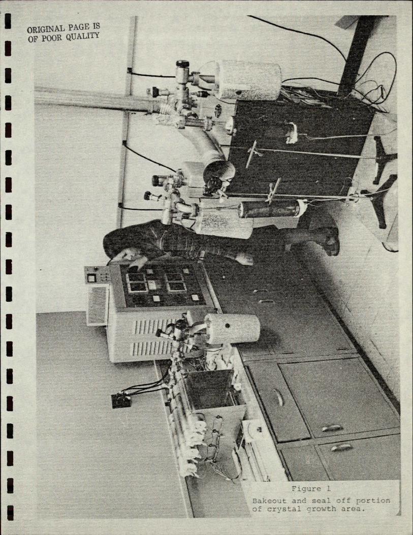
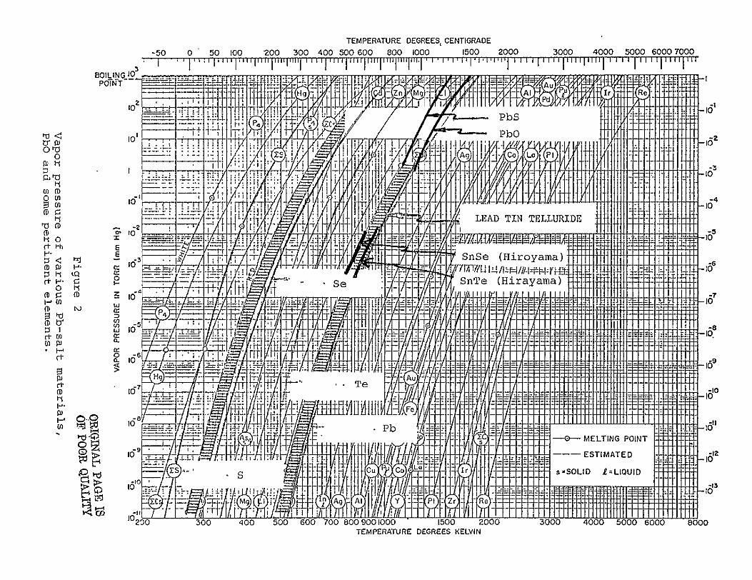
0
o 0
0 0
0 T
0 0o
C C
010
TO To0
TO
0
14shy
0 i
0
000
QR
IINA
PA
GE IS
Figure
OR
5r
23
UL
TVapo
prssur b-slt mterals
ofvarous
PbO
an soeFaien lmns
In the time allocated for this investigation in
the present program only PbSe was sublimed and this was combined
with an ingot of SnSe prepared by usual methods (ingot 1184) The
first attempt at crystal growth using 1184 failed because of
extremely rapid transport to the coolest region of the growth
ampoule with consequent polycrystalline structure A second
run was made at a temperature 150 lower than the usual growth
temperature This resulted in good quality crystals which howshy
ever were n-type (G137) A p-skin was formed with a 400C difshy
fusion and lasers were fabricated from the crystal Laser action
was not observed in any of the devices apparently because of a
deep irregular junction
The main result of this experiment is that the
crystal growth rate was significantly increased by pre-subliming
the PbSe giving strong support to the hypothesis that growth
inhibiting residual gas resides in the growth ingot In order
to utilize sublimed binaries all growth CID and pn-junction
parameters and oven profiles would have to be reestablished
It was estimated that these adjustments would require more time
and costs than were available in the scope of the program Thereshy
fore binary sublimation was not further included as part of the
program although it is being pursued at a lower level by Laser
Analytics
216 Summary of Growth Runs
During this program a total of 18 binary or
ternary source ingots were prepared These ingots were used
either for crystal growth or for conversiondiffusion purposes
A summary of these ingots showing their composition (x-value)
ingot identification number purpose and crystal growth results
(where applicable) is shown in Table 1 Crystals G69 through 100
were grown in order to optimize both furnace growth and CID
parameters as well as to obtain material suitable for a wide
variety of laser frequencies
-7shy
--
--
Table 1
SUMMARY OF Pb xSnxSe INGOTS AND
CRYSTALS PREPARED OR USED DURING THE PROGRAM
Composition Growth (G) (x) Ingot No Or Purpose Growth Results
0042 187
0042 188
0026 189
0 193
0 I103
0031 1108
00125 1109
00321 1121
005 1122
0036 1128
0035 1130
0047 1140
0039 I144
0048 1184
0047 1192
0030 1193
0047 1200
0047 1204
0045 1233
00445 1247
G69
G70
G71
p-source
n-source
G83
G84
p-source
G95
G98
GI00
G106
G109
G137
G138
G1391
G142
G146
G156T
G196
fair
fair
fair
good
poor
good
good
good
good
quaternary
good
fair
fair
fair
good
good
good
This ingot was a quaternary source with composition
Pb0961Sn0039Te0005Se0995 perfectly lattice matched
to PbSe
This ingot was prepared from the binaries using sublimed PbSe
t These crystals were not grown on this program
amp -8-
Following growth the crystals were stored for
further processing Some of this processing involved annealing
of the crystals with other sources in order to achieve either
CID structures or pn-junctions As the growths were carried out
in avariety of furnaces and under slightly different conditions
somewhat different growth results were generally obtained Only
onegrowth resulted in poor unuseable crystals Fair crysshy
tals were generally either smaller than usual or had a number of
visible grain boundaries Good crystals were moderate in size
(at least 3 mm on aside) and exhibited few if any grain bounshy
daries
Crystal G106 was subjected to the CID process
and used in the fabrication of four high performance lasers deshy
scribed in Section 4 Its composition was chosen to provide
lasers at specific wavelengths of interest to NASA
Growths G138 G142 and G146 were intended to
be exact duplicates of G106 to demonstrate reproducibility
While G138 and G142 appeared to reproduce the growth process
adequately G146 grew n-type instead of p-type The reason for
this discrepancy is not known although it is suspected that it
resulted from an unknown donor impurity accidently introduced
during processing
G196 was grown to provide high performance
lasers at NASA specified wavelengths
-9shy
22 Compositional Interdiffusion (CID)
221 Background
The CID method was developed by Laser Analytics
as an alternative relatively simple method of forming heteroshy
structures without the use of liquid-phase-epitaxy (LPE) or
molecular beam epitaxy (MBE) techniques While the latter techshy
niques have shown promise for forming heterostructures in the Pbshy
salts [56] they are considerably more complex to carry out and
the resulting lasers have exhibited severe reliability and lifeshy
time problems [781
The essential idea of the CID method is to anshy
neal a crystal of PblxSnxSe (or other Pb-salt ternary compound)
in the presence of a Pb1ySny Se vapor source where yltx Outshy
diffusion of the more volatile SnSe from the surface then proshy
duces a surface layer deficient in SnSe and thus possessing a
wider bandgap than the bulk The resulting structure is a single
heterobarrier In combination with a pn-junction as illustrated
in Figure 3 this structure then comprises a single-sided
heterojunction The high p-concentration of the bulk region comshy
pared to the much lower n-concentration in the diffused layer
ensures efficient injection into the confinement regions between
the heterobarrier and pn-junction
222 Techniques Employed
The CID procedure is generally carried out with
as-grown crystals of Pb lxSnxSe sealed in pre-cleaned and vacuumshy
baked quartz ampoules with poly-crystalline source ingots of
desired composition The typical processing temperature is 6001C
with heterobarrier depth controlled by annealing time assuming
the depth is proportional-to the square root of annealing time
Cool-down to room temperature is accomplished by rapid airshy
quench
ISORIGNo0L PKGF
OF pOOR QUALITY-10-
REGION 1 REGION 21 REGION 3
N-CID N-BULK I P-BULK
METALILAYER IERMI
CONDUCTION BAND
VALENCE BAND
_I
AT I ON ITENSITY
I
O1G~E~PAGE~I~jTEDI II Y
TER
TRAT ION
Figure 3
xSnxSe CID laser with pn-junction deeper thanteel of Pb
t CID region All x-axes represent distance below surface
oj crystal
Pn-junction diffusion may be performed simulshy
taneously with heterobarrier formation by using a source ingot
of opposite carrier type from the bulk Since the junction
movement proceeds by the rapid interdiffusion process whereas
the composition changes by self-diffusion the junction depth is
expected to be deeper than the heterobarrier as desired
223 Experimental Verification of the CID Process
To verify the occurance the CID effect and obtain
useful design parameters an electron beam microprobe (EBM) analyshy
sis was made of a CID-prepared structure The composition of the
as-giown p-type crystal before CID was Pb0955Sn0045 Se It
was sealed as described above with a source ingot of chalcogenideshy
rich Pb099Sn00 0 1 Se and annealed for six hours at 600C The
crystal has then cleaved and polished on a plane perpendicular
to the surface and microprobed along the polished face from the
surface into the bulk region Results of this EBM analysis are
shown in Figure 4 The existence of the CID effect is clearly
evident in that the composition of the crystal has been changed
to that of the source ingot for a distance extending approximately
5 pm into the bulk The apparent 2 pm width of the transistion
region represents the resolution limit of the microprobe
A diffusion coefficient is easily calculated
from the results of Figure 4 assuming that the diffusion depth
DDwhere t = the diffusion time and D the diffusion coefficient-11 2 The result is D = 12 x 10 cm sec The self-diffusion coeffishy
cient of Pb in Se-saturated PbSe at the same temperature obtained 10- 1cm by radioactive trace techniques was reported to be 16 x
sec [9] The close correspondence-of these results gives excelshy
lent support to the hypothesis that the CID effect results from
the self-diffusion of the metal constituent
-1shy
100
90
PbSe
801 region of SnSe outshydiffusion I
4-
4-I bulk
955 0 4 5 0o
20
SnSe 10
0 2 4 6 8 10 12 14
distance below surface (pm)
Figure 4 Composition vs distance into wafer for a Pb 955Sn 045Se
crystal interdiffused with Pb 0 9 9 9 Sn 0 0 0 1 Se at 6000C for 6
hours
Or P9
It is significant to note that the self-diffusion
coefficient of Pb in Pb-saturated PbSe is more than two ordersshy
of-magnitude less than that in Se-saturated PbSe Thus it is
expected that the heterobarrier depth in n-type material will be
much shallower than p-type
224 Lattice Matching Experiment
One aspect of heterostructure design to be conshy
sidered is the possibility of lattice mismatch between the layers
of different composition This may lead to strains and defects
within the crystal hence to device degradation Figure 5
shows the lattice constant variation for PblxSnxSe with
0 lt x lt 01 [1011] For the example of Figure 4 it may be
seen that the mismatch is less than 01 and even for Ax=0l
is only 016 From experience with III-V compound lasers [12]
mismatches of this magnitude would not be expected to be a problem
but the possibility cannot be overlooked
Attention was given to the potential lattice
mismatch problem in that a perfectly lattice matched structure
was fabricated This structure was achieved by utilizing the
fact that the two ternary systems Pbl xSnxSe and PblxSnxTe are
completely miscible over most of their composition range and
the addition of Te produces a larger lattice constant without
a significant change in bandgap This is illustrated in
Figure 6 which shows the lattice constant vs composition x y
for the quaternary system PblxSnxTelySey [1314] A large
range of perfectly lattice matched structures can be achieved In the work described here a PblxSnxTe ySey composition was
chosen to give emission near 12 pm and be perfectly lattice
matched to PbSe This composition was Pb096Sn0039Te0005Se0995
(as indicated in Table 1) and an ingot of this composition (G109)
was vapor grown The details of this lattice match are shown in
Figure 7 which is a blow-up of the lower right hand corner
of Figure 6 This crystal was interdiffused with PbSe to give
the lattice matched structure Point A represents the composition
-12shy
9 I613 -
1175CMEG
-o EG 810 cm
~E G =525 cm-1
= 612 U
611 0 02 04 06 08 01
x
Figure 5
Lattice constant (300K) of the Pb xSn xSe system for
0 lt x _ lt _ 01 E g values shown are at 12K
CM oO O
65LO If C3 L Pb Te
to0 64 - L
64 z
z Snco 62
0xwX 60
10 8 6 4 2 0
RPb- x SnxTe1y Se y
Figure 6 Lattice constant of the quaternary system PbJxSnxTel1ySey
showing iso-energy gap lines superimposed
6140 0
o IN
0610 0I-0C1
Co
0lt0
z 0 6120 X
_o 6110 Pb I Sn xTea S1yII-- - -
I-I
6100 1
010 005 0
Figure 7
Enlarged PbSe-corner of Figure 6 showing perfect lattice
matching between 12 pm quaternary material and pure PbSe
ORIGINAL PAGishyoF PoOR QUALUX
of ingot G109 while Point B represents the interdiffusediPbSe
region
Crystals of moderate size were grown from G109
Under microscopic examination large numbers of low-angle grain
boundaries were observed on the as-grown surfaces The cleavage
properties of the crystals were extremely poor and devices
fabricated from this did not exhibit laser action In view of
these poor initial results and NASAs expressed interest in obshy
taining high performance devices in a relatively short time
period this approach was not further pursued
23 Pn-Junction Diffusion
Pn-junction formation for this program was based on
control of stoichiometry deviations without the use of foreign
impurities For diffusion into p-type Pb1 -xSnxSe crystals the
vapor source was metal-saturated Pb1 -xSnxSe Movement of the
junction proceeds by interdiffusion which is generally orders
of magnitude faster than the self-diffusion mechanism governing
the CID process This difference in rates between the CID and
3unction diffusion processes makes it possible to control the
heterobarrier and pn-junction depths separately
Junction diffusions were carried out in evacuated
sealed quartz ampoules with the source ingot retained in an
inner quartz container to prevent physical contact with the -crystal Diffusion temperatures were in the range of 400o
600 0C and diffusion times from one to several hours Diffusion
depths were estimated from published values of interdiffusion
coefficients for the same condition [-9] In a number of cases
crystals were deliberately converted to opposite type using the
diffusion process Table 2 summarizes diffusion runs and conshy
versions carried as part of or in connection with this program
-13shy
Table 2 summarizes the diffusion runs and convershy
sions carried out in this program The original crystal growth
numbers are included as are performance characteristics of
lasers fabricated from these runs
OF
-14shy
Table 2
DIFFUSION RUN PARAMETERS
Growth
G No x-Value
95 0050
106 0047
138 0047
139 0030
142 0047
146 0047
156 0045
196 00445
D No
184
201
217
286
259
262
297
258
343
367
295
298
312
334
296
Diffusion
Type
Junction
Junction
Junction
Junction
Junction
Conversion
Junction
Junction
Conversion
Junction
Junction
Conversion
Junction
Junction
Junction
0 T(C) t(hr)
600 1
600 1
600 1
600 1
600 1
550 240
600 1
600 1
550 120
400 1
425 1
600 144
400 1
400 1
400 1
ORIGINAL PAGE IS OF POOR QUALITY
-15shy
30 DEVICE FABRICATION
31 Crystal Processing -
Following crystal growth useable facets were removed
by either slicing or cleaving Slicing was carried out with the
standard Laser Analytics procedure by use of a wire saw using
an abrasive slurry With proper use this method was found to
result in a minimum of crystal damage The cleaving method on
the other hand often leads to the introduction of crystal damage
most noticeable in the visible appearance of slip-lines along
[100] directions This latter method while considerably less
time-consuming than the slicing technique has therefore been
discontinued Wafers were typically sliced to thicknesses of
the order of 1 to 1-12 mm so as to allow enough material to
be subsequently removed to eliminate all saw damage Such saw
damage can propagate at least 1 or 2 orders of magnitude deeper
than the coarseness of the 5 pm grit used for cutting
32 Stripe Formation and Diffusion
After completion of the slicing operation the wafers
were ready for application of the insulator and definition of the
stripe pattern for formation of the stripe geometry junction
regions The general techniques for the formation of the stripes
involve evaporation of the insulator onto the wafer surface
through a metal mask which has a stripe pattern previously deshy
fined The resolution of this technique is more than adequate
to define 50 pm wide stripes (which has been a standard stripe
width at Laser Analytics)
After application of the diffusion mask the samples
were loaded immediately into a diffusion capsule together with
the diffusion source The capsules were evacuated sealed and
placed in the diffusion furnace
-16shy
33 Metallization
After diffusion the wafers were mounted with the
diffused side down and lapped and polished to a final thickness
of approximately 250 tim This procedure involved the use of
several slurry sizes each progressively finer than the preshy
vious one followed by a standard Laser Analytics final etching
The wafers were then loaded into the evaporator and metallized
with Au or CrAu on the p-side and In on the n-side Typical 0
metal thicknesses of 1000-2000A were used Cr was originally
contemplated because of its tendency to adsorb oxygen or oxides
and therefore provide a more tenacious metallurgical bond to the
Pb-salt material -This has in fact been verified and Cr
generally results in contact resistance values as low as those
observed for Au (typically 0005 to 0010 ohms corresponding - 6 2 to an RfA product of 1-2 x 10 ohm cm
A summary of the wafer processing operations carried
out to this point is given in Figure 8 After the final operashy
tion (step 6 in Figure 8) the wafers were cleaved into dice
34 End Face Cleaving
The metallized wafers were then mounted in special
cleaving fixtures and cleaved into individual laser dice A
photograph of the stations designed for wafer cleaving and die
mounting is shown in Figure 9 A schematic illustration of the
appearance of a laser die after this cleaving procedure is
shown in Figure 10 The laser dice were typically 14 mm
thick x 14 mm wide x 12 mm long
-17shy
WIES WCUTI AS-_GROWN FACET APPEARANCE OF WAFER AFTEARSAING OUTWFR GROWTH
P-N JUNCO
3CROSS SECTION OF WAFER SHOWING DIFFUSED REGIONS
5 FOLLOWING METALLIZATION OF THE JUNCTION SIDE
Figure 8
JDIFFUSION MATERIAL
2 APPEARANCE OF WAFER AFTER EVAPORATION OF DIFFUSION MASK MATERIAL
LAPPED SIDE
4 FOLLOWING WAFER LAPPING TO 250 UM THICKNESS
6 FOLLOWING METALLIZATION OF THE BACK SIDE
Summary of the wafer processing operations used in Pb-salt diode laser fabrication
OR1GINA pAGF 1
OF POOR QUALIT
U
I t
I I4 I I I il 1
S
Igt
i
ohmic contact insulator
heterolayer
pn junction substrate ohmic contact
Figure 10
Illustration of appearance of laser die after cleaving prior to package mounting
35 Die Mounting in Packages
The laser dice described in the previous section were
mounted with the striped side down on the copper laser stud
This provided for optimal thermal properties since the heat
generated near the shallow junction region was most readily reshy
moved in this manner The thermal resistance properties of this
configuration on the junction side can be obtained by reference
to Figure 11 The total thermal resistance 0T is given by
0T In + 0S
Where 0In is that due to the In metal contact (whose thickness
L is approximately 25 pm) and S is the spreading resistance into
the OFHC copper stud Assuming the thermal conductivity of indium
at 10K is 3 WcmK[15] and the contact area is 13 x 10- 3cm 2
the thermal resistance 0In = 07 KW The spreading resistance
term GS is given by [16]
0S = 2KM
where K is the thermal conductivity of the OFHC copper which is
approximately 5 WcmK and M is the linear dimension of one side
of the area approximately 14 mm Thus
0 ~ 5KW
The total expected thermal resistance of this configuration is
approximately 6 KW In practice this value has been found to
be of the order of 5-10 KW being influenced by thermal resisshy
tance values associated with the stud-to-package contacts as
well as the fact that actual laser dice are mounted at the edge
of the stud This model has also neglected heat removal from
the back side of the laser die but the calculated value is
nevertheless in general agreement with that observed in most
lasers
-18- ORIGINAL PAGE 18
OF POOR QUALITY
LASER DIE
- PN-JUNCTION
I N CONTACT AREA A
oFL45 13 x 10-3CM
OFHC COPPER STUD
Figure 11
Diagram illustrating thermal resistance calculation for diode lasers
I L2
I
Figure 12
SEM photograph of a typical laser die as mounted in the
the heat sink package The photograph was taken by
the NASA Langley Research Center
Dr John Buckley of
fMag = 45X
uOiGll4 pAGE 18)y p014 QUA
A photograph of a typical laser chip mounted in a
heat sink package is shown in Figure 12 This photograph taken
with an SEM [17] at a magnification of 45X shows the emitting
end of the laser pointing towards the right front The spongy
appearance of the top contact is due to the relatively thick In
plated on this electrode prior to laser assembly The small
overhang of the laser end over the sloped portion of the laser
stud is deliberate so as to prevent the shallow junction region
from being buried in the In plating on the top part of the stud
36 Experimental Package Studies
As a part of the overall objective of improving all
aspects of diode laser performance a preliminary investigation
was made into new methods of making electrical contact to the
laser dice Two new approaches werd considered 1) low temshy
perature soldering and 2) wire bonding
In the first approach lasers mounted in packages by
standard procedures were raised in temperature to slightly above
the melting point of indium (1551C) by placing them in a preshy
heated temperature controlled bath of purified stearic acid
After the melting step the lasers were cleaned in hot trichlorshy
ethylene and subjected to standard cleaving procedures Fiye
different devices were fabricated by the technique In every
case the electrical characteristics remained essentially unshy
changed but laser action was completely quenched It was apshy
parent that this heating process introduced crystalline strains
in the die which quenched laser action While lower temperature
solders are available previous results have indicated that they
either do not have the desirable wetting properties of In or
exist in a two-phase form which segregates in the small quantishy
ties involved in laser fabrication
-19shy
The second approach was a wire-bond technique using
a 0003 diameter gold wire soldered to a shortened top electrode
and pressure-contacted to the laser die It was felt that this
contact would remove the major contact induced strains in the
crystal Pressure was applied with controlled weights on a
piston fixture After several optimization attempts a laser
was successfully fabricated by this technique and delivered to
NASA Langley ResearchCenter (Serial No 6271-3) However the
contact failed during operation and the laser was subsequently
replaced We believe this method has promise but will require
the use of specialized die-bonding equipment and considerable
development time to effect
-20shy
40 LASER EVALUATION
41 Evaluation Methods
411 Dip Stick Testing for Electrical Characterization
The electrical characteristics of the diode lasers
were studied by pltting the I-V curves using a 4-point probe
technique designed to eliminate lead resistance effects The lasers
were mounted in an evacuated dip stick which could be immersed in
a liquid helium reservoir A GeCu infrared detector mounted in
the dipstick made it possible to measure the threshold current
of the laser and obtain an estimate of theoutput power
As an illustration-of the technique a typical
I-V curve of a high performance Pb09555Sn 0445Se CID device is
shown in Figure 3 (This laser was fabricated from crystal G196)
This I-V curve exhibits the slope discontinuity at threshold which
is typical for high performance Pb-salt lasers and indicative of
high internal quantum efficiency [18] The value of the voltage
intercept as shown in Figure 13 is 1045 mV (corresponding to
842 cm- ) in reasonable agreement with the laser threshold freshy-quency of826 cm I observed during subsequent optical testing of
the laser emission More information on the optical charactershy
istics of this device is given in the following section
A photograph of the dipstick test area is shown
in Figure 14 The dipsticks are evacuated after laser mounting
using the cryopumps shown in the figure The test arrangement
is such that 2 lasers can be mounted in each dipstick These
-21shy
__
__________
OF pOOR QUALITYORIG~hIAL PAGE IS
-Fshy
+ _I_ _____ --- -- --- ______ _ _ _ __--
-K - __ -__ __ __ ____-__
- - r I Elctial carceri cs of r----f I F -- ___
- -- -I pa---- -i--- 1K th st aAg t l n ---- =___-_-- - -shy
curv extrapolates ____ _ ono th
t 1 t _ ____
he sjar___
fige ure 13raoats E _ ___ __ __ _c _ -- _ _ x __I
an ____zrEh~zto 104SmV corresponding to _
F- iexpected laser emission of
42 cm nearthreshold -- shy
2D_
________ _________ _- t n~ g t l n o -
t__-- thIta E 1 K _
___ tio urve extapolates ___ 1_v__f 72lfl ___of the - - - - - -=-_
- --- cresodigtoato14m t
II p
IA
I I i I-I
La
e
Tig
ure 14
Laser
Dip
sti k
Testin
g
Area
dipsticks also proved useful for the thermal cycling tests
(described later) since the lasers are located in a vacuum enshy
closure and are therefore protected from moisture condensation
412 Evaluation of Emission Characteristics
The diode lasers fabricated during this program
were studied for a variety of optical performance characteristics
including
Threshold current vs temperature
Output power vs temperature
Spectral distribution vs temperature
Output power vs current
Limited measurements of tuning rate far-field spatial output
distribution and noise were also carried out
4121 Spectral Characteristics
The system used for the majority of
these measurements is diagrammed in Figure 15 The lasers were
mounted in a Laser Analytics Model TCR Stable Temperature Closed
Cycle Refrigerator which allows temperatures to be varied from
10K up to room temperature The collecting element was a corshy
rected fl KRS-5 lens with microadjustment Laser mode charactershy
istics were measured with a 12 meter grating monochromator and
the radiation was detected with a cooled HgCdTe infrared detector
The power output was measured with a 1-cm diameter pyroelectric
detector which could be shifted into the optical path
behind the chopper using a mirror arrangement The power meter
was supplied by the National Bureau of Standards Boulder Colorado
The lasers were powered by a Laser Analytics Model LCM Laser
-22shy
DETECTOR INFRARED LOCK-IN CRYOGENIC BIAS DETECTOR AM
TEMPERATURE X- _ STABILIZER RECORDEI
R LECTOR LENS
POWER CRO METERL RASE A GRATING
COOLE iMONOCHROMATORKRS-5
F1 CHOPPER DRUM LENS
SLASER CONTROL
MODULE
Figure 15
Schematic diagram of equipment used for evaluating optical
characteristics of diode lasers fabricated during the
program
Control Module The output of the system was displayed on both
an oscilloscope and an XY-recorder
As an exaEmple of the spectral measureshy
ments carried out during this program the spectral charactershy
istics observed from laser -7075-12 discussed in the previous section
are shown in Figure 16 The threshold frequency of this laser
-is 826 cm in close agreement with that obtained from the zeroshy
current intercept of the extrapolated value of the linear portion
of the I-V characteristics This laser had a maximum CW output
power of 105 mW per end at 127K At 20K the laser ran single
mode with an output power of 088 mW
4122 Spatial Profile Measurement
An Amperex pyroelectric vidicon was
used for preliminary measurements of the spatial distribution
The vidicon sensitivity is such that when the far field pattern
is spread over 50 of its receiving surface it can sense about
50 i-watts of infrared power The laser utilized for-this preshy
liminary experiment was a Pb0 97Sn0 03Se CID device from Laser
Analytics stock The laser was operated in a square wave mode
to provide the required AC signal Results obtained in this
manner are shown in Figure 17 The photograph of the CRT was
taken as the vidicon was slowly moved across the optical path
This mode of operation enhances the display contrast but care
must be taken to interpret this data Adjacent regions of dark
and bright areas correspond to regions of radiation intensity
the bright areas corresponding to the leading edge of travel (the
heating period) and the dark areas corresponding to the trailing
-23shy
LASER ANALYTICS INC 38 HARTWELL AVE
Grating SU Factor )79o Order2 Teperature Sensor -i3 0 LEXINGTON MASS 02173 I ------- bull
- I I shy=
- - = AIthP A
I --- - Ii - ----shy-
I - - (
T
S-------------
1 TIth~- -- --
---
-
-----------
-----shy
---
T 7
T--IIUthh~shy --plusmn - -
-----= I I -A
--- -shy - --shy
------- -------- T- =1_ i--------------T
S T - - = --- uL -7 lt - -------shy
7 1 - - I
9797- -fj 3 ii 1 I
th QFigure 16 th
Mode structure of laser 7075- - I = [ i ------------
--
C12 at 10K 20OK 40K 60K and 75K All spectra were taken - ---------------shyat 2 amps ------r------------shy
Atlt 4
NOR f 1 M Arl-
or n p
Tu44gt
TAW4
4 isVih
iA
0 All
11 4i
I r5 Iamp
+ 4 Ptnira 1
Wri1 ataat10pW 0 agt9 zcar
M4o
)4t 4
44A~ 17 gt~ 444 4
The small bright spot on the right edge (the cooling period)
half of the photograph was due to an imperfection on the vidicon
surface
An important aspect of this experiment
is that concentricrings due to diffraction effects associated
with the refrigerator window nearly mask the laser beam pattern
This result corroborates earlier measurements made by scanning
detector techniques Similar patterns have been reported for
GaAs lasers beamed through external diffraction structures [191
Circumvention of window effects to achieve a reliable measurement
of the spatial pattern would require the use of wedged windows
with anti-relfection coatings Time and cost restraints prevented
the enactment of these remedies hence these measurements were
not further pursued
42 Electrical and Optical Performance Results of Lasers
Delivered to NASA Langley Research Center
A total of nine lasers were delivered to NASA Langley
Research Center during this program Each of the following sections
contains the following information for each laser delivered
(a) I-V characteristics at lOK and 77K
(b) Emission spectra at various temperatures and at
2 amps
(c) Tables summarizing the variation of threshold
current output power (2A) and output frequency
(2A)
-24shy
421 Laser No 7028-6
(a) Electrical characteristics (Figure 18)
(b) Spectral data (Figure 19)
(c) Table of Ith Pout and frequency vs
temperature (Table 3)
-25shy
___
oRIBINAL PAGE JS OF POOR QUALITY
7028-6Laser No 0 3x = 0
R = 005 ohms
IFshy
_ _ __ =shy_ __-_ _ _
------ shy---- - - _ -
_t- I -I -shy
__ Ft ---= _ iv___ ~~~__ _ - - __
El crcl hrceristics
- r--r77K _---shy__ _
7Z 77K 7
--
LASER ANAL CS INC 38 HARTWELL AVE
Grating__- - Factor 896 Order I Temperature Sensor 2 5 LEXINGTON MASS 02173 I JU- - JL -I----iI- F F -- =
=I -I-J I -- I-- - - F0 shyt III ILL-II I L j hZth~C C shyt__j _Lplusmn_LI iLWJ - ---I
-IJ miP-I =oq-JjI 4-LLt~z-Utb- - --=oWh- -- L i - IH - --L L iD 6 IPJl Ill shy- P 3 r I-0Hq37i~itIflh1S7L1i41
-~Lwvt-iII 1 1]li~tt LF7 gt_- -- shy1 +4=t I_ _iJL I- -- --
I- I I [IFjIE_II da
I--- III - __~j- ltIII-- I LIwI--J--I---- t III L 1 ~ j t
T tI - J- IhI tI t
ltL- - 11 -LHPltE--_____-__1 1IIIIHIHiA9 plusmn_L plusmn1 -LL plusmn1I-Ph -L - - _ - -1 d-
-iI --- - - -L j I-I
i_ _+I_ +__ Iplusmn_IE_ V_ i-p- ___--_j --_ - -T
FMI-ki i I In ----- I_- + -- j- -H5-l- shy ---- ---- = - --iT- I -I J-1+ II ___riIILL
-i---------- II t ItH --- i tth21 -lit r ]j = IT - ---
- _
-II--I- HL
Figure 19 --- ----- -- Spectral output vs 0 ra- I -_shy
temperature for laser 70286ili - - -- c I -T t-l--r-l
I
Table 3
SUMMARY OF OPTICAL DATA FOR LASER 7028-6
2-Amp2-AMpSingleEndedOutputFrequencySingle-EndedLaser Package CW OutputIthTemperature Range (cm
(K) (mA) Power (mW)
867- 952043962010
961- 978035161020
1049l1060026357740
1150-1155007060060
OPIGINAL PAGE 18
OF PO1R QUALITY
422 Laser No 6271-2
(a) Electrical characteristics (Figure 20)
(b) Spectral data (Figure 21)
(c) Table of Ith Pout and frequency vs
temperature (Table 4)
-26shy
ORIGINALPAE1 OpPBOOR QUALMT
~~ aer No- 6271-2
000 5
H ohm
f R 03
R HI
~~~~~~~~~~~~~~~~~~~~~
shy r--n-rr+amp-
laser
+ 4 Eectrcalharateriticsof-shy
6212t10nd7K
2o 4o61
LASER ANALWIS INC 38 HARTWELL AVE
Grating _ p
Factcr Order Temperature Sensor 3 go LEXINGTON MASS 02173
----- - - - -shy
3[t l [ th--- ---
- i---- tW -t---- - - - - t
T+- P i
--
449
Q -T
i P-H -i-H
t - --
H I------I=
T o( S
- -------------
T -1-I ITT---
D4 it
- = --
- -shy-
1- In
IL I-- E-1T--
igure 21 h tth
temperature
P = Spectral output vs for laser op r t n62712
P =
Table 4
SUMMARY OF OPTICAL DATA FOR LASER 6271-2
2-Amp- output2-AmpSigl-Ende Laser Package Single-Ended Frequency Temperature th CW Output -I
(K) (mA) Power (mW) Range (cm
10 400 0132 727-741
20 490 0105 735-746
40 840 0088 776-788
-60 1540 ~002 851-860
65 1900 -001 875-877
O IJ
423 Laser No 7067-5
(a) Electrical characteristics (Figure 22)
(b) Spectral data (Figure 23)
(c) Table of Ith Pout and frequency vs
temperature (Table 5)
-27shy
--
--
ORIGINAL PAGE I8 OF POOR QUALIY
Laser No 7067-5
x = 00445
Sf= 00145 ohms
_QCshy
- _---__I
_ __
Figure 22
Electrical characteritc of laser 6067-5 at 10K-and 77K
Syj Zo6 -o )O
- --- ----- - -
LASER ANA4 CS INC HARTWELLAVEL 38X G
5 7-O Order Temperature Sensor _ L NGTON_MASS 0217 3 Grating Factor
-plusmn = o4 kK - S ATELAEKt~ l it tKqi-- - -
Ii4 i--1 - - - I _ - ------- t ---- - -shy
t h I--I- --- - U----
TflTI I4- I Ishy
-- i 1 - ----- --I-IP A
- -th=th th
IL 2 --- -shyt- HP-----
S_ THI
Ii - I -Ht F L-JL - _ ~ t - --th ---shy
] I -plusmn- Iplusmn i 7J +F- 2 I~~
t- igur 2= - - -Jdc-th -I- --
- HutuiSecrl oeatn -S mj 4l_r____- Hii[-ITi
PFigure 231=~~~~- IAi-tWLplusmn - ~i --- ---- Specal output vs operating LIt LWUlterperature for laser 7067-5 - I-iT jFI + - - tI I - -- 1iI ---- --
I HII I I 111111 I ___ L-------iI 11
Table 5
SUMMARY OF OPTICAL DATA FOR LASER 7067-5
2-Amp2-AmpSingleEndedOutputFrequencySingle-EndedLaser Package CW Output1thTemperature shy
(K) (mA) Power (mW) Range (cm I
841-85305060010
909002190048
1S0910GE op QIJMS1
424 Laser No 7067-7
(a) Electrical characteristics (Figure 24)
(b) Spectral data (Figure 25)
(c) Table of Ith Pout and Frequency
vs Temperature (Table 6)
-28shy
OIGINAL PAGE IS
OF POOR QUALITY
Laser No 7067-7
x = 00445
RF- 0023 ohms
- -
d
nFigure 24
_ Electrical characteristics -- of laser 7067-7 at 10K and
It _ - - - -
[6 20dego
LASER ANAYtCS INC 38 HARTWELL AVE
Grating
F actor 7 Order
-- T =
Temperature Sensor
T
lj
- --
LEXINGTON MASS 02173 I
-
th -L- - --- 2t
]th t[j ~ i- 1 -l--H - - - 4 -
_=-h0 - IV
jiP tti--yiplusmn
4 t
th -shy
t 2 gt7J-- --- -
ll- tt ----shy w t jj i I = = - -I-
~- - - ------ --
th
-
p8V
---
_
-
I~L I I =-
I -m-r-shy-L---HT- I=
- --I i
_1-t4 ij_hlIth -
-z
--shy [7
I
-t
- h
F-
- I1 4
1ttt
SS e ta oup t v-pe a i g i __ --I I -
P7 te pe at r fo_ l s 7067 7T= -H+FI I - I I gt 7 lt 1 II ilL I~~L +-I
71771rI- u _ t
T - shy---
------shy
----shy-- 1
Spectral output vs operating temperature for laser 7067-7 -
- plusmn P1 -
i-i -1----i-----I--- E---shy
Table 6
SUMMARY OF OPTICAL DATA FOR LASER 7067-7
2-Amp 2-Amp Output
Laser Package Single-Ended Frequency Temperature th CW -otput
(K) (mA) Power (mW) Range (cm
10 800 0246 834-860
20 860 0175 846-864
36 1480 002 895
ORIGINAL PAGE I1 OF POOR QUALITY
425 Laser No 7075-12
(a) Electrical characteristics (Figure 26)
(b) Spectral data (Figure 27)
(c) Table of Ith Pout and Frequency vs
Temperature (Table 7)
-29shy
OF pouh R
Laser 7075-12
x 00445
Rf 0025
_I 4
I I
26 Figure
CharacteristicsElectrical of laser 7075-12 at
10K and
77K
02D404QA CteAI
LASER ANAI1t S INC - 38 HARTWELL AVE
LEXINGTON MASS 02173pGrating 4 Factor T7B rder r TemperatureSensor Q3amp0
- -t -- aco - - rd - 2v
T T 7 T
- P
~ itIhI th=lg
1rI 2 - th =th=shy
-t -- -- shy Ltemperature-for p-+-- taserW7075-12
Ill(DT
Spectral output vs operatingr -shytemperature for laser 7075-12 P
Table 7
SUMMARY OF OPTICAL DATA FOR LASER 7075-12
Laser Package Temperature
(K)
10
20
40
60
75
th (mA)
440
480
820
1260
1850
2-AmpSigl-Ende Single-Ended CW output Power (mW)
105
0877
0263
0175
002
2-AmpOutput Frequency
Range (cm
826-829
832
874-884
947-949
1011
ORIGImNAL PAGE IS OF POOR QuALfij
426 Laser No 7109-6
Cal Electrical characteristics (Figure 28)
Cb) Spectral data (Figure 29)
(c) Table of Ith Pout and Frequency vs
Temperature (Table 8)
-30shy
ORIGINAT PAGE IS OF POOR QUJALITY
H-1 Laser 7109-6
i 700445
Hf o02 ohms
v
k
Elecrica
Chractrisics
t
Et
HH
I p
20L
--
D LASER ANAgt25 INC 38 HARTWELL AVE
Grating A Factor4 deg Order Temperature Sensor 3 ( LEXINGTON MASS 02173
T T= S- T =
Ith =QIth = (DmI = I =
6-1
-SP --
-I~II
T T
-T 4-1 1
I - F9
T shy-- IILI ____
- - - - - - - - - s -bull - P- N rtinh I- J ------ t h-shy h -MI I it
=
I Fiur 29SetaOuptV-tprt 4tIl-QwV tepeatr for~ laserI- 7109--- --shyi~ -- -I~~~~~- 3~t sect k
T= I -I- I-- - r -shy -- j-
Table 8
SUMMARY OF OPTICAL DATA FOR LASER 7109-6
2-Amp
Laser Package Temperature
(K)
th (mA)
Sg2-Amp Single-Ended CW Output Power (mW)
output Frequency
-1 Range (cm
10 590 0570 812-864
20 690 0526 852
30 1100 0044 869
32 1900 002 869-890
ORIGINAL PAGE IS OF POOR QUAITY
427 Laser No 7111-3
(a) Electrical characteristics (Figure 30)
(b) Spectral data (Figure 31)
(c) Table of Ith Pout and Frequency vs
Temperature (table 9)
-31shy
Laser No 7111-3
=T-= x = 00445
Rf= 00135 ohms
E e
t
i
a
S
~z
ri
E
H rr
r -
I
-
rr
- I
i
P k
70
ORGIA
01
PAGE
0
is
le
II ORGIA PIG lOOR 1
__
---------
-- --
-LASER ANAUS IN(38 HARTWELL AVE
LEXINGTON MASS 02173 Grating _Factor 8c6 Order Temperature SensorjikZZ 1-1 T = T T
th i- (E
P PO -
- -y i=i=D 1 ith
--- - - - - -IT-
tI-- shy
- -- t--I--------
tt~I -t
-- - - -
th---
-1--~~x -- - -r
v -- i-S pu - t
-+) 1 0r--r-
1-empert fo- l
t 88+8 oo+cflamp__
-N
Table 9
SUMMARY OF OPTICAL DATA FOR LASER 7111-3
2-Amp
Laser Package Temperature(K)
Ith(mA)
2Am Single-EndedCW OutputPower (mW)
Output Frequency-1Range (cm
10 1400 0263 820-831
20 1700 0263 829-838
40 1880 003 888-895
Oolt
428 Laser No 7061-1
(a) Electrical characteristics (Figure 32)
(b) Spectral data (Figure 33)
(c) Table of Ith POut and Frequency vs
Temperature (Table 10)
-32shy
II
ORIGINAL PAGE IS OF POOR QUALITY
_- __=___
xo047 _ _~_________-- -r_~~Rf 0022 ohms -
FEshy
= ~~~~~-- u--- _Lf__f-i_
_
4- L-
IrIshy
~~Figure 32 +kshy
~Electrical characteristics _ __
H of laser -7061-1 at 10K and
- 77K _- _ -shy
-i ----shy I
-- -
-------- -
----- -- - -
i
LASER ANALYTICS 38 HARTWELL AVE
INC
Gtalting (Sp- Factor Order I Temperature Sensor 9ampoR SLWS 20 LEXINGTON MASS 02173
T -L--------
Iiit+L= ---
LL1- -T-0--f - -shyz
Il -----
tt -
-3
H(DAL
- --- hI 1-1 21 i~ --------
IIt
IiK 1 I7-I7 -11 + - [+L3 T I - i
1-i-I--l4 Tth = H 215-i L1I
-Ii----------------P
I L o
T ------ -=--shy
-- - I--------- 0 3
]E -ll -i F- -i--T S e t a ou p t v ng
Itemperature for laser 7061shybull - ---i -- --- -------- _-A4i--------shy7-~~---- 4 --- -----I--
Table 10
SUMMARY OF OPTICAL DATA FOR LASER NO 7061-1
Laser Package Temperature
(K)
10
20
40
60
80
95
th
(mA)
148
158
200
333
680
1520
2-Amp2-AmpSingle-Ended CW Output
Power (mW)
07
07
07
08
06
01
Output Frequency
- IRange (cm 1
770-796
780-800
825-851
894-906
974-1006
1045-1051
429 Laser No 7069-1
(a) Electrical characteristics (Figure 34)
(b) Spectral data (Figure 35)
(c) Table of Ithm Pout and Frequency vs
Temperature (Table 11)
-33shy
_____
----
__
- _I ------
1 _ 7069-r _ Laser
x 0047 1 -- +-shy
f 0027 ohms
t_L___________________-____=Eshy ___
-I -I
_shy- -- H- --~-
7__1_ _ 1L - -- -E
_-_-- ME INshy
_ _
4+- shy_ _- _--
_ - _--
- gt
-- shy 34~~~~Figure
~~Electrical characteristics--i
anoflaser 7069-1 at 10 and-
10
77K
1t0RoeuroT
LASER ANALY ILCS INC 38 HARTWELL AVE
Grating I ) 6f7)Order Teperature Sensor 9 9 LEXINGTON MASS 02173LA-Factor I -- -I -
----- ------ 0 th-n-- yF--- -- - - - - - - --o - - -~ w i-
_th-I = 2t j -v th 3 I= P Ca
iI-I- I - I-------------------]
Th- _z ~I
- -- output iLLL- - - ---peer
VV
----------------------- I ---- 11 x
--shy
0MIshy
th H - - t-ishy
fF- I rplusmn
-11-t -V -I-j -
-----------------
IthH
-1 J-~f T1- Fiur 35 [ 11 ---- Spectral output operatnshy----- vs
-- temperature for laser 7069- --shy
j-4-1- shy
-i
Table i
SUMMARY OF OPTICAL DATA FOR LASER NO 7Q69-
Laser Package
Temperature (K)
10
20
40
60
80
Ith (mA)
122
135
190
332
709
2-AmpSingle-Ended
CW Output Power (mW)
009
009
013
009
-002
2-AmpOutput
-u Range (cm
771-797
782-802
833-849
927-1006
1052-1089
ORIGINAL pAGE IS
OF poop QUALITY
43 Summary and Discussion of Laser Performance Data
Important operating characteristics are summarized in
Table 12 for the lasers whose properties are given in Section 43
above and for two additional devices discussed in the next secshy
tion The following observations are significant
1) Four out of the twelve lasers in Table 12 had CW
operating temperatures above the boiling point of liquid nitrogen
2) Eight out of the twelve- lasers had CW operating
tepperatures in excess of 60K
3) Five of the lasers in Table 12 had CW singleshy
ended power outputs greater than 05 milliwatts
4) Four out of the twelve lasers exibited single mode
CW single-ended power in excess of 05 milliwatts
5) CW operation above liquid nitrogen temperature has
been achieved at wavelengths as long as 1035 pm (the longest
wavelength previously peported for operation of any diode laser
at 77K or above is 96 pm [19] 1
These results represent a substantial improvement in
the state-of-the-art of tunable diode lasers in the 8-15 pm specshy
tral range Previous homojunction lasers -in this range have
generally had maximum operating temperatures below 40K have
never exhibited 77K operation and have consistently produced
maximum CW power outputs of less than 05 milliwatts overall
The CID technology can now be used on a reproducible basis in
both the PbSSe and the PbSnSe systems
The results of the present progtam show that the CID
technology can be used to provide significantly improved pershy
formance on a reproducible basis throughout the 8-15 pm range
-34shy
Table 12
PERFORMANCE CHARACTERISTICS SUMMARY FOR LASERS
PREPARED AND EVALUATED DURING THE PROGRAM
Maximum Maximum CW Single Tuning
Crystal Junction Date Operating Ended Power Range Laser Growth Diffusion Delivered to Temperature Output R -I
x-Value No NASALangley (K) (mW) at T(K) (cmSerial No Run No
6271-2 95 05 184 32377- 65 01 12 726827
6271-3 95 05 184 32377-1-1- 60 01 720-864
726-9666313-3 106 047 201 85 04
1 6315-2 106 047 201 - 85 12 800-1051
7028-6 139 03 258 2277 60 04 13 867-115460 766-1051286 61577 95 08
7061-1 106 047 7067-1 196 0445 296 32377 48 05 13 841-853
7067-7 196 0445 296 32377 36 02 13 834-895
7069-1 138 047 297 61577 80 01 40 742-1089
7075-12 196 0445 296 32377 75 10 13 826r1011
7109-6 196 0445 296 42577 32 06 13 812-883
7111-3 156 045 334 42577 40 03 20 820-895
1 Returned for repair due to single strand lead wire fracture Returned aftertepair
It This laser fabricated in an experimental wire-contact configuration failed at NASALangley
and was returned to LAI
This x-value indicates the material composition Pb1 xSnxSe
Not delivered Used in reliabilitylifetime studies described in Section 45
This is the temperature at which the laser output power decreased to approximately 0009 pW
44 Reliability and Lifetime Studies
A number of failure and degradation mechanisms were
observed and addressed during the course of this program The
following paragraphs discuss these problems and solutions which
have been developed
441 Package Relaxation
During this and other Laser Analytics programs
it was found that a number of lasers exhibited a pronounced inshy
crease in series resistance after a few temperature cyclings beshy
tween room and cryogenic temperatures It was discovered that
the effort resulted from the relaxation of laser package parts
which had been strained at initial assembly This problem was
overcome by straightforward design modifications involving addishy
tion of a second set-screw Figure 36 shows a demonstration of
cycling behavior in which a laser was cycled from 300K to 77K
twenty times-with no change in electrical characteristics
442 Crystal Degradation
The term crystal degradation refers to a failure
mode apparently associated with the laser crystal or its deposited
metal layers rather than the package As an example Laser No
7061-1 was stored at room temperature and shipped more than four
months after initial assembly its electrical characteristics at
the time of shipping were given in Figure 32 Figure 37 shows
the electrical characteristics on the date of assembly for comshy
parison It is apparent that during the four-month storage
period the series resistance increased from 6 milliohms to
22 milliohms and the threshold current from 0110 amps to
-
0455 amps
-36shy
OtIGINAL PAGE IS OF POOR QUALITY
As another example Laser No 6313-3 had a
series resistance of 10 milliohms and threshold current of
082 amps at assembly After three months the series resisshy
tance increased to 61 milliohms but the threshold current deshy
creased to 060 amps This threshold reduction dan be related
to a decrease in a pronounced excess current near zero bias
The excess current is thought to be related to surface effects which become less pronounced with time This laser was subseshy
quently destroyed in an attempt to re-seat it in the package
As a third and extreme example Laser No
6315-2 completely failed within a time of one month
443 Low Temperature Storage and Operation
Three high performance CID devices were stored
in liquid nitrogen for varying periods of time Results are
shown in Table 13 The conclusion can be made that negligible
degradation occurs during cryogenic storage
Qualitative observations at our laboratory and
by a number of purchasers of Laser Analytics lasers leads to
the conclusion that high performancePb-salt-lasers do-not deshy
grade for-indefinitely long periods of operation as long as
they are maintained at cryogenic temperature
444 Discussion
Lifetime and reliability problems have in the
past been confused by a combination of effects occurring simulshy
taneously It now seems clear however that a crystal degrashy
dation problem does exist in Pb-salt heterojunction devices
The effect is much more pronounced in MBE and LPE heterojuncshy
tions but is also significant in CID A report on this subject
-37shy
Table 13
LIFETIME STUDIES OF HIGH PERFORMANCE PblxSnxSe CID LASERS
STORED AT LIQUID NITROGEN TEMPERATURE
Rf (42K)Ith (42K)Storage Time (amps) (milliohms)
Laser at 77K After After Serial No x-Value (Months) Initial Storage Initial Storage Comments
76315-1 0047 3 046 046 80 80
7068-1 0030 3 046 052 90 110 Increased Ith related to increased excess current
7068-2 0030 2 038 036 170 170 Decreased Ith related to decreased excess current
-with recommendation for action has been submitted to NASA by
Laser Analytics [21]
Since the effect is most pronounced with heteroshy
junctions it is likely to be associated with lattice mismatching
Thus one solution may be to further perfect the quaternary
growth procedures discussed previously Alternatively an opshy
timization of the degree of lattice mismatch may be possible
the tradeoff would be the height of the heterobarrier
Finally if a short range solution should not
be feasible a practical fall-back position is to maintain the
lasers at or below liquid nitrogen temperature continually
-39shy
-4-4-4
+ -r r4 t
tli1m fi
V4M
C ti LIM fIN Tl ZfK
-----------
ORIGINAL PAGE IS OF POOR QUALITY -
9 ---0 -- --- 1 - -F- - - -- -shy
-oo - - --- I 1 - - + - _ _- -+ = a--- - -- = - i--t--- -t - k -_ + _
t i - I -
r - t =
1 -
- r--+ - EZ--- r - - ----I - - - --- F h--zshy
Io- shy
r - 7_- 1 at- t -
-- - I t J ti i i [V]
time of fabricat ion
--- - -
--- --
50 CONCLUSIONS AND RECOMMENDATIONS FOR FURTHER WORK
51 Results
The central result of this program is that theCID
Technique has been successfully applied to produce single heteroshy
junction Pb-salt diode lasers with significantly improved pershy
formance Single-modeCW power outputs as high as -05 milliwatts
have been achieved at an operating temperature of 20K and CW
operationabove 77K has been obtained for wavelengths as long
as 1036 pm Ten laserswere delivered to NASA under the conshy
tract of which two operated CW above 77K and seven above 60K
Two additional lasers operating above 77K were fabricated and
used in reliabilitylifetime studies These results represent
a significant advance over earlier homojunction methods which
typically result in maximum attainable single mode CW power
nilliwatts and maximum operating temperaturesmuch less than 01
less than 40K
Contact degradation manifested by increased series reshy
sistance and consequentialperformance degradation was noted
and explored Significant progress was made in definingthe -
effect Astop-gap solution to degradation problemswas found
to be storage at liquid nitrogen temperature
5-2 Recommendations
Continued work with CID structures should include a
systematic study of both pn-junction and heterobarrier diffusion
properties At the present time the carrier confinement width
is only qualitatively known or controllable An improved strucshy
ture with confinement widths of less than 1 pm may result in
very substantial improvements in both output power and operating
temperature In addition to an improved confinement structure
control of junction and barrier depths will allow optimization
of junction depth with regard to thermal properties Pn-junction
-40shy
diffusion depths can be measured by angle-lapping and probing
techniques Heterobarrier depths require an EMB system for efshy
fective measurement
Investigations into reducing the barrier height differshy
entialby using a more closely matched x-value in the CID difshy
fusion source may reduce lattice mismatch problems andimprove
room temperature storage properties Alternatively further
research into quaternary compound formation may result in zero
lattice mismatch
The sublimed binary experiment indicated that crystal
growth procedures are not optimum and that new purification
techniques may result in greatly improved crystal quality
It is strongly recommended that a systematic investishy
gation into reliability and lifetime questions be immediately
instituted and vigorously pursued
Noise properties of diode lasers areimperfectly
characterized and not well understood A systematic investigashy
tion of noise and instabilities in tunable diode lasers would be
of considerable value
Preliminary investigations of liquid phase epitaxy
(LPE) have indicated high performance devices can be obtained
While reliability and yield problems presently dominate this
technology future efforts aimed at obtaining a better undershy
standing of these phenomena are indicated For the long range
double heterostructures are expected to result in devices subshy
stantially better than single heterostructures
The above recommendations are believed to be of parshy
ticular importance as a result of the findings of the present
program Other important areas to pursue include 1) improvement
ORIGJINA pAGFI 1S - 4O QUAUW
of contact metallization procedures 2) new packaging techniques
3) stripe-width optimization 4) development of anti-reflection
coatings and 5) investigation of controlled doping by foreign
impurities
-42shy
60 REFERENCES
1 KJ Linden KW Nill and JF Butler IEEE Journal of
Quantum Electronics August 1977 (to be published)
2 AR Calawa TC Harman M Finn and P Youtz Trans AIME
242 374 (1968)
3 TC Harman and Ivars Melngailis Applied Solid State
Science R Wolfe editor Academic Press New York
(1974)
4 TC Harman and JP McVittie Jour Electronic Materials
3 843 (1974)
5 SH Groves KW Nill and AJ Strauss Appl Phys Lett
25 331 (197-4)
6 JN Walpole AR Calawa TC Harman and SH Groves
Appl Phys Lett 2-8 552 (1976)
7 JN Walpole private communication
8 KW Nill and SH Groves private communication
9 RW Broderson JN Walpole and AR Calawa J Appi
Phys 41 1484 (1970)
10 S Yamamoto Science Reports Tohoku University 40 11 (1956)
11 M Neuberger IV-VI Ternary Semiconducting Compound Data
Tables EPIC-S16 p- 22 March (1976)
12 MH Pilkuhn and H Rupprecht J Appl Phys 38 5 (1967)
-43shy
13 CA Kennedy and KJ Linden J Appl Phys 41 252 (1970)
14 L Laugier J Cadoz M Faure and M Moulin J Crystal
Growth 21 235 (1974)
15 R Radebaugh Rev Sci Instr 48 93 (1977)
16 R Scapple Sol State Tech 74 April (1974)
17 SEM photos were taken by Dr John Buckley of the NASA
Langley Research Center
18 JN Walpole AR Calawa RW Ralston TC Harman and
JP McVittie Appl Phys Lett 23 620 (1973)
19 i Hayashi Appl Phys 5 25 (1974)
20 ED Hinkley RTKu KW Nill and JF Butler Appl
Optics 15 1653 (1976)
21 Laser Analytics -ReportLAI 77-2-9 February 15 1977
-44shy
APPENDIX A
A portion of the results of this program was included in the
following article
Single Heterostructure Lasers of PbS lxSex and Pbl1 x
Sn Se With Wide Tunabilityx
K J Linden K W Nil and J F Butler
Journal of Quantum Electronics (to be published in
August 1977)
720 IEEE JOURNAL OF QUANTUM ELECTRONICS VOL QE-13 NO 8 AUGUST 1977
Single Heterostructure Lasers of PbSl-xSex and Pbl-xSnxSe with Wide Tunability
K J LINDEN MEMBER IEEE K WNILL MEMBER IEEE AND J F BUTLER SENIOR MEMBER IEEE
Abstrcr-Single-heterostrueture diode lasers formed by composi-tional interdiffusion in PbS_xSe and Pb1 xSnxSe and by liquidshyphase-epitaxy (LPE) in Pbl SnSe show performance characteristics _ significantly better than those observed in conventional homostmeture lasers Higher operating temperatures were obtained for all composi-
tions with CW operation above 77 K being achieved for compositions corresponding to wavelengths from 41 to 127 Arm Single-ended CW powers as high as 70 oW corresponding to lext = 44 percent were ob-served in PbSi _Se devices
I INTRODUCTION
T HE TERNARY Pb-salt semiconductors Pb1-CdS PbS-Se- and Pb-xSnSe provide tunable diode lasers0
throughout the infrared region of 3-30 pm These lasers are finding a growing use in spectroscopy-related applications where they provide measurement capability far beyond that of conventional instruments In spectral absorption studies for
example they allow measurements with a resolution better than 10 4 -cm which is many orders of magnitude better than conventional instruments [1] For monitoring air pollutants and other trace gases they offer the prospect of long-path measurements sensitivity in the sub-ppb range and the ability to discriminate between interfering species to a degree com-pletely unattainable by conventional techniques [2] Further
interest has been generated by their use as local oscillators in heterodyne -receivers for infrared astronomy [3] stratospheric ozone monitoring [4] and other uses
Widespread utilization of Pb-salt lasers has in the past been hindered by their very low operating temperatures typically 30 K or less Improvements in fabrication techniques to be de- scribed in this paper substantially increase operating tempera-tures and in particular make operation of these lasers above 77 K a reality for the spectral range from 4 pm to at least 127 pm These higher operating temperatures both extend the temperature tuning range for laser spectrometry applica-tions and greatly simplify the cooling apparatus requirements in fixed-wavelength monitoring instruments The improved performance results from the development of new techniques to form single-heterostructure diode lasers of PbSi-xSeX and Pb -SnSe Most of the results are based on the use of a new technique compositional Interdiffusion (CID) although pre-limmary results for liquid-phase-epitaxy (LPE) heterostructures in lib -SnSe are also reported
Manuscript received March 22 1977 Portions of this work were supshyported by NASA-LangleyResearch Center Hampton VA
The authors ae with Laser Analytics Inc Lexington MA 02173
100
90o PbSe
8o region of SnSe outshydiffuson I
I
b
- Pb955Sn co45u
gt20
o SnSe
2 4 6 8 10 12 14
ditnce below surface (ion)
Fig 1 Compositional interdiffusion (CID) effect as determined by electron-beam meroprobe analysis of PbogssSno04 SSe dafer anshy-nealed with Pbog9SnooiSe source at 600C for 65 hours
II HETEROSTRUCTURE FORMATION BY CID
-CID is a technique that involves the creation of a single hetshyerostructure in any pseudobinary compound in whichthevapor pressures of the binary constituents are different [5] In the case of Pb-salt chalcogenides the vapor pressure of the low band-gap binary constituent is greater than that of the high band-gap binary constituent [6] [7] Thus by annealing a crystal of Pb-xSnSe with x = xi in a closed ampoule toshygether with a source of composition x = x2 such that x gt x 2
the surface composition of the crystal will change to-that of x The depth ofthe composition change is dependent on the time and temperature of the anneal Ajunction may be formed either during the interdiffusion or as a separate operation Typically a CID of 6 hours at 600degC results in a depth of 5 um The junction depth can then be tailored to any desired value by a subsequent diffusion The CID effect has been exshyperimentally verified by electron microprobe analysis as illusshytrated in Fig 1 [8] -
Single heterostructures were formed by CID in p-type crysshytals Stripe geomefiy p-n junctions were subsequently proshyduced by diffusion through a diffusion mask forming 50-prfi wide stripes Control of stoichiometry was used for carriershyconcentration control and p-n junction formation Ohmic conshytacts were made with Au and In on the p- and n-sides respecshytively The laser chips were formed by cleaving along [100]
tEBM analysis was carried out by A J Strauss and MC Finn of the MIT Lincoln Laboratory
Copyrightcopy1977 by The Institute of Electrical and Electronics Engineers Inc Printed in USA Annals No 708QE035
- -
721 LINDEN er at SINGLE HETEROSTRUCTURE LASERS
Fig 2 Pb-salt diode laser package designed to provide heat sinking on
both sides of laser chip
surfaces to final dimensions With typically -400 pmn between2 end-faces The lasers were mounted in packages designedfor efficient heat removal from both sides of the chips A laser mounted in its -package is illustrated in Fig 2 Laser tuning data indicate that thermal resistances -of lasers mounted in these packages is of the order of 1KW at 12 K
III PbS1 -Se DIODE LASERS FORMED BY CID
CID diode lasers have been fabricated from PbS_Se throughout the entire compositional range The as-grown crys-
tals were n-type and were type-converted by a lugh-temperature
anneal in the presence of a Sl-Se-rich source ingot The crystals were then heated m the presence of a Pb-rich diffusion
source to simultaneously produce a CID heterostructure and a p-n junction
Lasers fabricated from these crystals generally exhibited high quantum efficiencies with low threshold currents and low se-ries resistance values The electrical I-V characteristics of a high-performance CID PbSosSeo laser are shown in Fig 3 A pronounced slope discontinuity is exhibited at threshold im-plying high internal quantum efficiency [9] This behavior is observed in all our heterostructure Pb-salt lasers For this laser
the series resistance is less than 5 ma The variation in thresh-old current and emission frequency with temperature of a typ-ical PbSo8Se0 2 CID diode laser is shown in Fig 4 Table I summarizes the operating characteristics of this device and six others fabricated from the same crystal The series resistances
T= 0K
Cl
100 200 300
voltage mv
Fig 3 Electrical characteristics of PbSo8Se02 diode laser at 10 K Deshymm longvice active area is 50 gn wide by 05
of these devices varied from 5 to 15 m 2 and threshold currents from 45 to 130 mA
The maximum operating temperature we have observed for a PbS_Se CID laser operating CW at 2 A is 130 K achieved with PbS0o 3Seo97 This device exhibited a CW single-ended power output of 70 mW corresponding to rfext = 44 percent
IV Pb1 -SnSe DIODE LASERS FABRICATED BY CID
Pb1 _Sox e single-heterostructure CID lasers have Been fabshyricated with x ranging from zero to 021 The latter composishytion is beyond that of the well-known energy-band cross-over [10] Pb1 -SnSe lasers with compositions in this range tune to lower frequencies with increasing temperature
722 IEEE JOURNAL OF QUANTUM ELECTRONICS VOL QE-13 NO 8 AUGUST 1977
2400
PbS 8e2
next 134 2300 2lt2
2200
2100frequec
th - _1 2025
0 10 20 20 40 50 60 70 80 90
temperatue K
Fig 4 Variation of threshold current and output frequency with temshy
perature for PbSosSeo2 laser ORIGINAL PAGE IS OF POOR QUALITY
TABLE I PROPERTIES OF PbSo Seo CID DIODE LASERS
TuningSingle-Ended RangesnextCW Power OutLaser No (milliwatts) () max(K) (cm 1)
1 135 48 90 2060-2460
2 22 08 77 2030-2330
3 31 12 30 2035-2100
4 378 134 89 2035-2365
5 136 50 70 2047-2269
6 55 18 60 2047-2312
7 350 124 89 2040-2385
TABLE II SUMMARY OF ELECTRICAL AND OPTICAl PERFORMANCE
CHARACTERISTICS OBSERVED IN WIDELY TuNABI E
Pb-SnSe CID-LASERS Tuning
exP T
max RangeLaser Rf(O) IthI
) P
3 No (10 Xl (10 L) (W) - I) (I (cn )
0011 7021-10 017 245 3940 29 95 1086-1396
0026 6275-1 006 350 3500 30 98 926-1228
0030 7031-3 005 450 789 06 100 892-1159
0047 6315-1 008 493 1230 13 95 768-1063
0065 - 6294-7 010 220 0660 07 45 590-733
01Os 6135-3 030 575 - 02- 50 420-580shy
7049-6 024 280 04 01 45 428-3310210
Estimated not measured
whereas Pb -SnSe lasers withx Z 015 tune inthe-opposite are in close agreement with the measured threshold frequencies1
of the laser at both temperaturesdirection The as-grown Pb1 xSnrSe crystals are p-type Fabrication Fig 6 shows details of the mode structure for a typical
procedures are qualitatively identical to those for PbS1 _Sex Pb1 _SaxSe CID laser as the temperature is varied The
lasers except for omission of the type-conversion step modes exhibit a well defined longitudinal structure with a spacshy--Some characteristics of high-performance Pb -xSnSe lasers ing of 2 cm 1 at 10K and 207 cm at 60 K corresponding
with a variety of compositions are summarized in Table II As to effective refractive indices of 625 and 603 respectively
is evident from this table lasers with compositional values of At 95 K the threshold current is 14 A and since the laser curshy
x lt 0047 operated at temperatures of up to 100 K The elec- rent is near threshold essentially single-mode operation occurs
trical characteristics of a Pbo9 1Sno0 3Se at both 10 and 77 K Fig 7 shows the variation of total multimde output
are shoWn in Fig 5 Both curves exhibit the characteristic power and frequency with operating temperature for a
slope (dIdV) discontinuity indicative of high internal quan- Pbo 9s3Sno0o41Se laser As the laser temperature is increased
turm efficiency As is typically the case the values of voltage- from 12 to 60 K the output-power increase of 20 percent is
intercept obtained from an ixtrapolation of the straight-line proportional to the 20 percent increase in output frequency quantum efficiency(series resistiuce-limited) portion of the electrical characteristic This is indicative of a nearly constant
723 LINDEN et al SINGLE HETEROSTRUCTURE LASERS
2
10K C 177K
0
0 100 200
voltage (mv)
Fig 5 Electrical I-V characteristics- of Pb0 9Sn0o03 Se laser at 10 and 77 K Extrapolated voltage intercept values correspond closely to the measured threshold frequency values at these temperatures
-fT 10K
-782 all c1
1 920 oaf
1
11067 cm 95
Frequency -
Fig 6 Mode structure of Pboss3Snouo4Se liser at 10 60 and 95 K All spectra were taken at2-A laser current
within this entire operating temperature region The range of laser tunability extends over 300 cm - from 1302 to 937pym with the region from 102 to 937 pm occurring-above liquid nitrogen temperature
V Pb 1 _SnSe LASERS FORMED BY LPE
Thissection presents the first reported results obtained from heterostructure lasers of Pb -SnxSe grown by LPE The epshyitaxial layers ofPbl xSnxSe were depositedon [100]oriented vapor grown Pbo93 4Sno066 Se substrates and stripe-geometry lasers were formed by diffusion masking techniques Perfor-mance characteristics of four lasers with operating temperatures above liquid nitrogen are summarized in Table III Electrical characteristics-of these devices also exhibited slope discontinu-ities indicative of high internal quantum efficiencies A plot of shytotal multimode CW output power per end (at 2-A operating current) together with laser frequency versus T is shown in Fig 8- In this case a 90 percent increase in output power between
2 Details will be described in a subsequent paper
12 and 60 K is observed corresponding to an increase in-exter nal quantum efficiency from 04 percent at 12 K to 06 pershy-cent at 60 K
The laser- shown in Fig 8 has a tuning range of 319 cm- covering the range from 1107 pm at 90 K to 1712 pim at 12 K This laser produces the longest reported diode laser wavelength (127 pm) atliquid nitrogen temperature
VI CONCLUSION
Single-heterostructure diode lasers of PbS _Se and Pb-xSnSe exhibit marked increases in operating temperature over previous homojunction lasers in these materials In par ticular operating temperatures of liquid nitrogen or above have been achieved at wavelengths as long as 127 pm In all wavelength regions large increases in temperature-tuning range result from higher attainable operating temperature
These higher operating temperatures greatly increase the useshyffulness of Pb-salt lasers in high-resolution spectrometry as a reshysult of their corresponding increased tuning range Perhaps of
greater potential significance relatively simple cooling techshy
724 IEEEJOURNAL OF QUANTUM ELECTRONICS VOL QE-13 NO 8 AUGUST 1977
125 - 1100
Power
100 1000
075 9007 vE
050 Frequency 800
o 025 700
0
10 50 100
Temperature (K)
Fig 7 Single-ended output power and frequency as afunction of opershyating temperature for Pbog 53 Sno4-7Se CID diode laser operating at 2 A
TABLE III SUMMARY OF PERFORMANCE CHARACTERISTICS OF PbO931SI10o66Se
STRIPE GEOMETRY LASERS FABRICATED BY LPE - llxiau c~Tunt ng
R almum CW Range)Laser f Output Power (KI (cmNo (ohms) Per End (nw) TMax I
6309-5 0012 053 90 584-903 6309-2 0006 026 80 605-921
6289-5 0003 - 002 85 626-867
6289-6 0070 2G as 623-854
OFJ 6
SI 9005
4s 800
bull a- oo=3-700 t
~frequency 2 - 600
0
10 50 100
temperature K
Fig 8 Single-ended output power and frequency as a function of opershyating temperature for Pbo9 34 Sno0 6 6Se LPE diode laser Laser curshyrent is 2 A
niques available at liquid nitrogen temperatures and above will Infrared heterodyne spectroscopy of astronomical and laborashynow make it practical to consider a variety of advanced tun- tory sources at 85 pm NASA Goddard Space Flight Center
document X0691-74-237 Aug 1974 able diode laser instruments for trace-gas monitoring and other [4] M A Frerking and D JMuehlner Infrared heterodyne specshy
applications troscopy of atmospheric ozone Appl Opt vol 16 pp 526shy528 1977
REFERENCES [S] E D Hinkley R T Ku K W Nilland J F Butler Long-path monitonng Advanced instrumentation with a tunable diode lashy
[1] E D Hinkley K W Nil and F A Blum Infrared spectroscopy serAppl Optvol 15pp 1653-1659 1976 with tunable lasers in Topics in Applied Physics vol 2 H [6] D A Northrup Vaporization in the PbTe-SnTe system J Walther Ed New York NY Springer-Verlag 1976 chapter 2 Electrochem Soc vol 118 pp 1365-1370 1971
[2] ED Hinkley andP L Kelley Detection of air pollutants with (7] C Hirayama Y Ichikawa and A M DeRoo Vapor pressures of tunable diode lasers Science vol 171 p 635 1971 tin selenide and tin telluride JPhys Chem vol 67pp 1039shy
[31 M Mumma T Kostiuk S Cohen D Buhl and P C VonThuna 1042 1963
725 LINDEN et al SINGLE HETEROSTRUCTURE LASERS
[8] K J Linden J F Butlerand K W N11 Single heterostiucture - P McVitte Single heterojunction Pb1 -xSnxTe diode lasers
tunable diode lasers formed by compositional mtexdiffusion in Appl PhysLet vol 23 pp 620-622 1973 IEEE Int Electron Devices Meeting-Tech Dig 1976 pp 132- [10] T C Harnan A R Calawa 1 Melngailis and J 0 Dimmock
135 Temperature and compositional dependence of laser emission in
[9) J N Walpole A R Calawa R W Ralston T C Herman and Pb SnxSeAppL Phys Lett vol 14 pp 333-334 1969
ORIGINAL PAGE IS OF POOR QUALUT
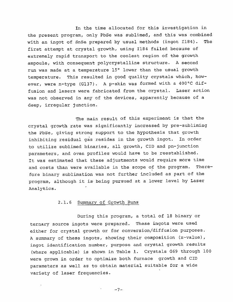

--
--
Table 1
SUMMARY OF Pb xSnxSe INGOTS AND
CRYSTALS PREPARED OR USED DURING THE PROGRAM
Composition Growth (G) (x) Ingot No Or Purpose Growth Results
0042 187
0042 188
0026 189
0 193
0 I103
0031 1108
00125 1109
00321 1121
005 1122
0036 1128
0035 1130
0047 1140
0039 I144
0048 1184
0047 1192
0030 1193
0047 1200
0047 1204
0045 1233
00445 1247
G69
G70
G71
p-source
n-source
G83
G84
p-source
G95
G98
GI00
G106
G109
G137
G138
G1391
G142
G146
G156T
G196
fair
fair
fair
good
poor
good
good
good
good
quaternary
good
fair
fair
fair
good
good
good
This ingot was a quaternary source with composition
Pb0961Sn0039Te0005Se0995 perfectly lattice matched
to PbSe
This ingot was prepared from the binaries using sublimed PbSe
t These crystals were not grown on this program
amp -8-
Following growth the crystals were stored for
further processing Some of this processing involved annealing
of the crystals with other sources in order to achieve either
CID structures or pn-junctions As the growths were carried out
in avariety of furnaces and under slightly different conditions
somewhat different growth results were generally obtained Only
onegrowth resulted in poor unuseable crystals Fair crysshy
tals were generally either smaller than usual or had a number of
visible grain boundaries Good crystals were moderate in size
(at least 3 mm on aside) and exhibited few if any grain bounshy
daries
Crystal G106 was subjected to the CID process
and used in the fabrication of four high performance lasers deshy
scribed in Section 4 Its composition was chosen to provide
lasers at specific wavelengths of interest to NASA
Growths G138 G142 and G146 were intended to
be exact duplicates of G106 to demonstrate reproducibility
While G138 and G142 appeared to reproduce the growth process
adequately G146 grew n-type instead of p-type The reason for
this discrepancy is not known although it is suspected that it
resulted from an unknown donor impurity accidently introduced
during processing
G196 was grown to provide high performance
lasers at NASA specified wavelengths
-9shy
22 Compositional Interdiffusion (CID)
221 Background
The CID method was developed by Laser Analytics
as an alternative relatively simple method of forming heteroshy
structures without the use of liquid-phase-epitaxy (LPE) or
molecular beam epitaxy (MBE) techniques While the latter techshy
niques have shown promise for forming heterostructures in the Pbshy
salts [56] they are considerably more complex to carry out and
the resulting lasers have exhibited severe reliability and lifeshy
time problems [781
The essential idea of the CID method is to anshy
neal a crystal of PblxSnxSe (or other Pb-salt ternary compound)
in the presence of a Pb1ySny Se vapor source where yltx Outshy
diffusion of the more volatile SnSe from the surface then proshy
duces a surface layer deficient in SnSe and thus possessing a
wider bandgap than the bulk The resulting structure is a single
heterobarrier In combination with a pn-junction as illustrated
in Figure 3 this structure then comprises a single-sided
heterojunction The high p-concentration of the bulk region comshy
pared to the much lower n-concentration in the diffused layer
ensures efficient injection into the confinement regions between
the heterobarrier and pn-junction
222 Techniques Employed
The CID procedure is generally carried out with
as-grown crystals of Pb lxSnxSe sealed in pre-cleaned and vacuumshy
baked quartz ampoules with poly-crystalline source ingots of
desired composition The typical processing temperature is 6001C
with heterobarrier depth controlled by annealing time assuming
the depth is proportional-to the square root of annealing time
Cool-down to room temperature is accomplished by rapid airshy
quench
ISORIGNo0L PKGF
OF pOOR QUALITY-10-
REGION 1 REGION 21 REGION 3
N-CID N-BULK I P-BULK
METALILAYER IERMI
CONDUCTION BAND
VALENCE BAND
_I
AT I ON ITENSITY
I
O1G~E~PAGE~I~jTEDI II Y
TER
TRAT ION
Figure 3
xSnxSe CID laser with pn-junction deeper thanteel of Pb
t CID region All x-axes represent distance below surface
oj crystal
Pn-junction diffusion may be performed simulshy
taneously with heterobarrier formation by using a source ingot
of opposite carrier type from the bulk Since the junction
movement proceeds by the rapid interdiffusion process whereas
the composition changes by self-diffusion the junction depth is
expected to be deeper than the heterobarrier as desired
223 Experimental Verification of the CID Process
To verify the occurance the CID effect and obtain
useful design parameters an electron beam microprobe (EBM) analyshy
sis was made of a CID-prepared structure The composition of the
as-giown p-type crystal before CID was Pb0955Sn0045 Se It
was sealed as described above with a source ingot of chalcogenideshy
rich Pb099Sn00 0 1 Se and annealed for six hours at 600C The
crystal has then cleaved and polished on a plane perpendicular
to the surface and microprobed along the polished face from the
surface into the bulk region Results of this EBM analysis are
shown in Figure 4 The existence of the CID effect is clearly
evident in that the composition of the crystal has been changed
to that of the source ingot for a distance extending approximately
5 pm into the bulk The apparent 2 pm width of the transistion
region represents the resolution limit of the microprobe
A diffusion coefficient is easily calculated
from the results of Figure 4 assuming that the diffusion depth
DDwhere t = the diffusion time and D the diffusion coefficient-11 2 The result is D = 12 x 10 cm sec The self-diffusion coeffishy
cient of Pb in Se-saturated PbSe at the same temperature obtained 10- 1cm by radioactive trace techniques was reported to be 16 x
sec [9] The close correspondence-of these results gives excelshy
lent support to the hypothesis that the CID effect results from
the self-diffusion of the metal constituent
-1shy
100
90
PbSe
801 region of SnSe outshydiffusion I
4-
4-I bulk
955 0 4 5 0o
20
SnSe 10
0 2 4 6 8 10 12 14
distance below surface (pm)
Figure 4 Composition vs distance into wafer for a Pb 955Sn 045Se
crystal interdiffused with Pb 0 9 9 9 Sn 0 0 0 1 Se at 6000C for 6
hours
Or P9
It is significant to note that the self-diffusion
coefficient of Pb in Pb-saturated PbSe is more than two ordersshy
of-magnitude less than that in Se-saturated PbSe Thus it is
expected that the heterobarrier depth in n-type material will be
much shallower than p-type
224 Lattice Matching Experiment
One aspect of heterostructure design to be conshy
sidered is the possibility of lattice mismatch between the layers
of different composition This may lead to strains and defects
within the crystal hence to device degradation Figure 5
shows the lattice constant variation for PblxSnxSe with
0 lt x lt 01 [1011] For the example of Figure 4 it may be
seen that the mismatch is less than 01 and even for Ax=0l
is only 016 From experience with III-V compound lasers [12]
mismatches of this magnitude would not be expected to be a problem
but the possibility cannot be overlooked
Attention was given to the potential lattice
mismatch problem in that a perfectly lattice matched structure
was fabricated This structure was achieved by utilizing the
fact that the two ternary systems Pbl xSnxSe and PblxSnxTe are
completely miscible over most of their composition range and
the addition of Te produces a larger lattice constant without
a significant change in bandgap This is illustrated in
Figure 6 which shows the lattice constant vs composition x y
for the quaternary system PblxSnxTelySey [1314] A large
range of perfectly lattice matched structures can be achieved In the work described here a PblxSnxTe ySey composition was
chosen to give emission near 12 pm and be perfectly lattice
matched to PbSe This composition was Pb096Sn0039Te0005Se0995
(as indicated in Table 1) and an ingot of this composition (G109)
was vapor grown The details of this lattice match are shown in
Figure 7 which is a blow-up of the lower right hand corner
of Figure 6 This crystal was interdiffused with PbSe to give
the lattice matched structure Point A represents the composition
-12shy
9 I613 -
1175CMEG
-o EG 810 cm
~E G =525 cm-1
= 612 U
611 0 02 04 06 08 01
x
Figure 5
Lattice constant (300K) of the Pb xSn xSe system for
0 lt x _ lt _ 01 E g values shown are at 12K
CM oO O
65LO If C3 L Pb Te
to0 64 - L
64 z
z Snco 62
0xwX 60
10 8 6 4 2 0
RPb- x SnxTe1y Se y
Figure 6 Lattice constant of the quaternary system PbJxSnxTel1ySey
showing iso-energy gap lines superimposed
6140 0
o IN
0610 0I-0C1
Co
0lt0
z 0 6120 X
_o 6110 Pb I Sn xTea S1yII-- - -
I-I
6100 1
010 005 0
Figure 7
Enlarged PbSe-corner of Figure 6 showing perfect lattice
matching between 12 pm quaternary material and pure PbSe
ORIGINAL PAGishyoF PoOR QUALUX
of ingot G109 while Point B represents the interdiffusediPbSe
region
Crystals of moderate size were grown from G109
Under microscopic examination large numbers of low-angle grain
boundaries were observed on the as-grown surfaces The cleavage
properties of the crystals were extremely poor and devices
fabricated from this did not exhibit laser action In view of
these poor initial results and NASAs expressed interest in obshy
taining high performance devices in a relatively short time
period this approach was not further pursued
23 Pn-Junction Diffusion
Pn-junction formation for this program was based on
control of stoichiometry deviations without the use of foreign
impurities For diffusion into p-type Pb1 -xSnxSe crystals the
vapor source was metal-saturated Pb1 -xSnxSe Movement of the
junction proceeds by interdiffusion which is generally orders
of magnitude faster than the self-diffusion mechanism governing
the CID process This difference in rates between the CID and
3unction diffusion processes makes it possible to control the
heterobarrier and pn-junction depths separately
Junction diffusions were carried out in evacuated
sealed quartz ampoules with the source ingot retained in an
inner quartz container to prevent physical contact with the -crystal Diffusion temperatures were in the range of 400o
600 0C and diffusion times from one to several hours Diffusion
depths were estimated from published values of interdiffusion
coefficients for the same condition [-9] In a number of cases
crystals were deliberately converted to opposite type using the
diffusion process Table 2 summarizes diffusion runs and conshy
versions carried as part of or in connection with this program
-13shy
Table 2 summarizes the diffusion runs and convershy
sions carried out in this program The original crystal growth
numbers are included as are performance characteristics of
lasers fabricated from these runs
OF
-14shy
Table 2
DIFFUSION RUN PARAMETERS
Growth
G No x-Value
95 0050
106 0047
138 0047
139 0030
142 0047
146 0047
156 0045
196 00445
D No
184
201
217
286
259
262
297
258
343
367
295
298
312
334
296
Diffusion
Type
Junction
Junction
Junction
Junction
Junction
Conversion
Junction
Junction
Conversion
Junction
Junction
Conversion
Junction
Junction
Junction
0 T(C) t(hr)
600 1
600 1
600 1
600 1
600 1
550 240
600 1
600 1
550 120
400 1
425 1
600 144
400 1
400 1
400 1
ORIGINAL PAGE IS OF POOR QUALITY
-15shy
30 DEVICE FABRICATION
31 Crystal Processing -
Following crystal growth useable facets were removed
by either slicing or cleaving Slicing was carried out with the
standard Laser Analytics procedure by use of a wire saw using
an abrasive slurry With proper use this method was found to
result in a minimum of crystal damage The cleaving method on
the other hand often leads to the introduction of crystal damage
most noticeable in the visible appearance of slip-lines along
[100] directions This latter method while considerably less
time-consuming than the slicing technique has therefore been
discontinued Wafers were typically sliced to thicknesses of
the order of 1 to 1-12 mm so as to allow enough material to
be subsequently removed to eliminate all saw damage Such saw
damage can propagate at least 1 or 2 orders of magnitude deeper
than the coarseness of the 5 pm grit used for cutting
32 Stripe Formation and Diffusion
After completion of the slicing operation the wafers
were ready for application of the insulator and definition of the
stripe pattern for formation of the stripe geometry junction
regions The general techniques for the formation of the stripes
involve evaporation of the insulator onto the wafer surface
through a metal mask which has a stripe pattern previously deshy
fined The resolution of this technique is more than adequate
to define 50 pm wide stripes (which has been a standard stripe
width at Laser Analytics)
After application of the diffusion mask the samples
were loaded immediately into a diffusion capsule together with
the diffusion source The capsules were evacuated sealed and
placed in the diffusion furnace
-16shy
33 Metallization
After diffusion the wafers were mounted with the
diffused side down and lapped and polished to a final thickness
of approximately 250 tim This procedure involved the use of
several slurry sizes each progressively finer than the preshy
vious one followed by a standard Laser Analytics final etching
The wafers were then loaded into the evaporator and metallized
with Au or CrAu on the p-side and In on the n-side Typical 0
metal thicknesses of 1000-2000A were used Cr was originally
contemplated because of its tendency to adsorb oxygen or oxides
and therefore provide a more tenacious metallurgical bond to the
Pb-salt material -This has in fact been verified and Cr
generally results in contact resistance values as low as those
observed for Au (typically 0005 to 0010 ohms corresponding - 6 2 to an RfA product of 1-2 x 10 ohm cm
A summary of the wafer processing operations carried
out to this point is given in Figure 8 After the final operashy
tion (step 6 in Figure 8) the wafers were cleaved into dice
34 End Face Cleaving
The metallized wafers were then mounted in special
cleaving fixtures and cleaved into individual laser dice A
photograph of the stations designed for wafer cleaving and die
mounting is shown in Figure 9 A schematic illustration of the
appearance of a laser die after this cleaving procedure is
shown in Figure 10 The laser dice were typically 14 mm
thick x 14 mm wide x 12 mm long
-17shy
WIES WCUTI AS-_GROWN FACET APPEARANCE OF WAFER AFTEARSAING OUTWFR GROWTH
P-N JUNCO
3CROSS SECTION OF WAFER SHOWING DIFFUSED REGIONS
5 FOLLOWING METALLIZATION OF THE JUNCTION SIDE
Figure 8
JDIFFUSION MATERIAL
2 APPEARANCE OF WAFER AFTER EVAPORATION OF DIFFUSION MASK MATERIAL
LAPPED SIDE
4 FOLLOWING WAFER LAPPING TO 250 UM THICKNESS
6 FOLLOWING METALLIZATION OF THE BACK SIDE
Summary of the wafer processing operations used in Pb-salt diode laser fabrication
OR1GINA pAGF 1
OF POOR QUALIT
U
I t
I I4 I I I il 1
S
Igt
i
ohmic contact insulator
heterolayer
pn junction substrate ohmic contact
Figure 10
Illustration of appearance of laser die after cleaving prior to package mounting
35 Die Mounting in Packages
The laser dice described in the previous section were
mounted with the striped side down on the copper laser stud
This provided for optimal thermal properties since the heat
generated near the shallow junction region was most readily reshy
moved in this manner The thermal resistance properties of this
configuration on the junction side can be obtained by reference
to Figure 11 The total thermal resistance 0T is given by
0T In + 0S
Where 0In is that due to the In metal contact (whose thickness
L is approximately 25 pm) and S is the spreading resistance into
the OFHC copper stud Assuming the thermal conductivity of indium
at 10K is 3 WcmK[15] and the contact area is 13 x 10- 3cm 2
the thermal resistance 0In = 07 KW The spreading resistance
term GS is given by [16]
0S = 2KM
where K is the thermal conductivity of the OFHC copper which is
approximately 5 WcmK and M is the linear dimension of one side
of the area approximately 14 mm Thus
0 ~ 5KW
The total expected thermal resistance of this configuration is
approximately 6 KW In practice this value has been found to
be of the order of 5-10 KW being influenced by thermal resisshy
tance values associated with the stud-to-package contacts as
well as the fact that actual laser dice are mounted at the edge
of the stud This model has also neglected heat removal from
the back side of the laser die but the calculated value is
nevertheless in general agreement with that observed in most
lasers
-18- ORIGINAL PAGE 18
OF POOR QUALITY
LASER DIE
- PN-JUNCTION
I N CONTACT AREA A
oFL45 13 x 10-3CM
OFHC COPPER STUD
Figure 11
Diagram illustrating thermal resistance calculation for diode lasers
I L2
I
Figure 12
SEM photograph of a typical laser die as mounted in the
the heat sink package The photograph was taken by
the NASA Langley Research Center
Dr John Buckley of
fMag = 45X
uOiGll4 pAGE 18)y p014 QUA
A photograph of a typical laser chip mounted in a
heat sink package is shown in Figure 12 This photograph taken
with an SEM [17] at a magnification of 45X shows the emitting
end of the laser pointing towards the right front The spongy
appearance of the top contact is due to the relatively thick In
plated on this electrode prior to laser assembly The small
overhang of the laser end over the sloped portion of the laser
stud is deliberate so as to prevent the shallow junction region
from being buried in the In plating on the top part of the stud
36 Experimental Package Studies
As a part of the overall objective of improving all
aspects of diode laser performance a preliminary investigation
was made into new methods of making electrical contact to the
laser dice Two new approaches werd considered 1) low temshy
perature soldering and 2) wire bonding
In the first approach lasers mounted in packages by
standard procedures were raised in temperature to slightly above
the melting point of indium (1551C) by placing them in a preshy
heated temperature controlled bath of purified stearic acid
After the melting step the lasers were cleaned in hot trichlorshy
ethylene and subjected to standard cleaving procedures Fiye
different devices were fabricated by the technique In every
case the electrical characteristics remained essentially unshy
changed but laser action was completely quenched It was apshy
parent that this heating process introduced crystalline strains
in the die which quenched laser action While lower temperature
solders are available previous results have indicated that they
either do not have the desirable wetting properties of In or
exist in a two-phase form which segregates in the small quantishy
ties involved in laser fabrication
-19shy
The second approach was a wire-bond technique using
a 0003 diameter gold wire soldered to a shortened top electrode
and pressure-contacted to the laser die It was felt that this
contact would remove the major contact induced strains in the
crystal Pressure was applied with controlled weights on a
piston fixture After several optimization attempts a laser
was successfully fabricated by this technique and delivered to
NASA Langley ResearchCenter (Serial No 6271-3) However the
contact failed during operation and the laser was subsequently
replaced We believe this method has promise but will require
the use of specialized die-bonding equipment and considerable
development time to effect
-20shy
40 LASER EVALUATION
41 Evaluation Methods
411 Dip Stick Testing for Electrical Characterization
The electrical characteristics of the diode lasers
were studied by pltting the I-V curves using a 4-point probe
technique designed to eliminate lead resistance effects The lasers
were mounted in an evacuated dip stick which could be immersed in
a liquid helium reservoir A GeCu infrared detector mounted in
the dipstick made it possible to measure the threshold current
of the laser and obtain an estimate of theoutput power
As an illustration-of the technique a typical
I-V curve of a high performance Pb09555Sn 0445Se CID device is
shown in Figure 3 (This laser was fabricated from crystal G196)
This I-V curve exhibits the slope discontinuity at threshold which
is typical for high performance Pb-salt lasers and indicative of
high internal quantum efficiency [18] The value of the voltage
intercept as shown in Figure 13 is 1045 mV (corresponding to
842 cm- ) in reasonable agreement with the laser threshold freshy-quency of826 cm I observed during subsequent optical testing of
the laser emission More information on the optical charactershy
istics of this device is given in the following section
A photograph of the dipstick test area is shown
in Figure 14 The dipsticks are evacuated after laser mounting
using the cryopumps shown in the figure The test arrangement
is such that 2 lasers can be mounted in each dipstick These
-21shy
__
__________
OF pOOR QUALITYORIG~hIAL PAGE IS
-Fshy
+ _I_ _____ --- -- --- ______ _ _ _ __--
-K - __ -__ __ __ ____-__
- - r I Elctial carceri cs of r----f I F -- ___
- -- -I pa---- -i--- 1K th st aAg t l n ---- =___-_-- - -shy
curv extrapolates ____ _ ono th
t 1 t _ ____
he sjar___
fige ure 13raoats E _ ___ __ __ _c _ -- _ _ x __I
an ____zrEh~zto 104SmV corresponding to _
F- iexpected laser emission of
42 cm nearthreshold -- shy
2D_
________ _________ _- t n~ g t l n o -
t__-- thIta E 1 K _
___ tio urve extapolates ___ 1_v__f 72lfl ___of the - - - - - -=-_
- --- cresodigtoato14m t
II p
IA
I I i I-I
La
e
Tig
ure 14
Laser
Dip
sti k
Testin
g
Area
dipsticks also proved useful for the thermal cycling tests
(described later) since the lasers are located in a vacuum enshy
closure and are therefore protected from moisture condensation
412 Evaluation of Emission Characteristics
The diode lasers fabricated during this program
were studied for a variety of optical performance characteristics
including
Threshold current vs temperature
Output power vs temperature
Spectral distribution vs temperature
Output power vs current
Limited measurements of tuning rate far-field spatial output
distribution and noise were also carried out
4121 Spectral Characteristics
The system used for the majority of
these measurements is diagrammed in Figure 15 The lasers were
mounted in a Laser Analytics Model TCR Stable Temperature Closed
Cycle Refrigerator which allows temperatures to be varied from
10K up to room temperature The collecting element was a corshy
rected fl KRS-5 lens with microadjustment Laser mode charactershy
istics were measured with a 12 meter grating monochromator and
the radiation was detected with a cooled HgCdTe infrared detector
The power output was measured with a 1-cm diameter pyroelectric
detector which could be shifted into the optical path
behind the chopper using a mirror arrangement The power meter
was supplied by the National Bureau of Standards Boulder Colorado
The lasers were powered by a Laser Analytics Model LCM Laser
-22shy
DETECTOR INFRARED LOCK-IN CRYOGENIC BIAS DETECTOR AM
TEMPERATURE X- _ STABILIZER RECORDEI
R LECTOR LENS
POWER CRO METERL RASE A GRATING
COOLE iMONOCHROMATORKRS-5
F1 CHOPPER DRUM LENS
SLASER CONTROL
MODULE
Figure 15
Schematic diagram of equipment used for evaluating optical
characteristics of diode lasers fabricated during the
program
Control Module The output of the system was displayed on both
an oscilloscope and an XY-recorder
As an exaEmple of the spectral measureshy
ments carried out during this program the spectral charactershy
istics observed from laser -7075-12 discussed in the previous section
are shown in Figure 16 The threshold frequency of this laser
-is 826 cm in close agreement with that obtained from the zeroshy
current intercept of the extrapolated value of the linear portion
of the I-V characteristics This laser had a maximum CW output
power of 105 mW per end at 127K At 20K the laser ran single
mode with an output power of 088 mW
4122 Spatial Profile Measurement
An Amperex pyroelectric vidicon was
used for preliminary measurements of the spatial distribution
The vidicon sensitivity is such that when the far field pattern
is spread over 50 of its receiving surface it can sense about
50 i-watts of infrared power The laser utilized for-this preshy
liminary experiment was a Pb0 97Sn0 03Se CID device from Laser
Analytics stock The laser was operated in a square wave mode
to provide the required AC signal Results obtained in this
manner are shown in Figure 17 The photograph of the CRT was
taken as the vidicon was slowly moved across the optical path
This mode of operation enhances the display contrast but care
must be taken to interpret this data Adjacent regions of dark
and bright areas correspond to regions of radiation intensity
the bright areas corresponding to the leading edge of travel (the
heating period) and the dark areas corresponding to the trailing
-23shy
LASER ANALYTICS INC 38 HARTWELL AVE
Grating SU Factor )79o Order2 Teperature Sensor -i3 0 LEXINGTON MASS 02173 I ------- bull
- I I shy=
- - = AIthP A
I --- - Ii - ----shy-
I - - (
T
S-------------
1 TIth~- -- --
---
-
-----------
-----shy
---
T 7
T--IIUthh~shy --plusmn - -
-----= I I -A
--- -shy - --shy
------- -------- T- =1_ i--------------T
S T - - = --- uL -7 lt - -------shy
7 1 - - I
9797- -fj 3 ii 1 I
th QFigure 16 th
Mode structure of laser 7075- - I = [ i ------------
--
C12 at 10K 20OK 40K 60K and 75K All spectra were taken - ---------------shyat 2 amps ------r------------shy
Atlt 4
NOR f 1 M Arl-
or n p
Tu44gt
TAW4
4 isVih
iA
0 All
11 4i
I r5 Iamp
+ 4 Ptnira 1
Wri1 ataat10pW 0 agt9 zcar
M4o
)4t 4
44A~ 17 gt~ 444 4
The small bright spot on the right edge (the cooling period)
half of the photograph was due to an imperfection on the vidicon
surface
An important aspect of this experiment
is that concentricrings due to diffraction effects associated
with the refrigerator window nearly mask the laser beam pattern
This result corroborates earlier measurements made by scanning
detector techniques Similar patterns have been reported for
GaAs lasers beamed through external diffraction structures [191
Circumvention of window effects to achieve a reliable measurement
of the spatial pattern would require the use of wedged windows
with anti-relfection coatings Time and cost restraints prevented
the enactment of these remedies hence these measurements were
not further pursued
42 Electrical and Optical Performance Results of Lasers
Delivered to NASA Langley Research Center
A total of nine lasers were delivered to NASA Langley
Research Center during this program Each of the following sections
contains the following information for each laser delivered
(a) I-V characteristics at lOK and 77K
(b) Emission spectra at various temperatures and at
2 amps
(c) Tables summarizing the variation of threshold
current output power (2A) and output frequency
(2A)
-24shy
421 Laser No 7028-6
(a) Electrical characteristics (Figure 18)
(b) Spectral data (Figure 19)
(c) Table of Ith Pout and frequency vs
temperature (Table 3)
-25shy
___
oRIBINAL PAGE JS OF POOR QUALITY
7028-6Laser No 0 3x = 0
R = 005 ohms
IFshy
_ _ __ =shy_ __-_ _ _
------ shy---- - - _ -
_t- I -I -shy
__ Ft ---= _ iv___ ~~~__ _ - - __
El crcl hrceristics
- r--r77K _---shy__ _
7Z 77K 7
--
LASER ANAL CS INC 38 HARTWELL AVE
Grating__- - Factor 896 Order I Temperature Sensor 2 5 LEXINGTON MASS 02173 I JU- - JL -I----iI- F F -- =
=I -I-J I -- I-- - - F0 shyt III ILL-II I L j hZth~C C shyt__j _Lplusmn_LI iLWJ - ---I
-IJ miP-I =oq-JjI 4-LLt~z-Utb- - --=oWh- -- L i - IH - --L L iD 6 IPJl Ill shy- P 3 r I-0Hq37i~itIflh1S7L1i41
-~Lwvt-iII 1 1]li~tt LF7 gt_- -- shy1 +4=t I_ _iJL I- -- --
I- I I [IFjIE_II da
I--- III - __~j- ltIII-- I LIwI--J--I---- t III L 1 ~ j t
T tI - J- IhI tI t
ltL- - 11 -LHPltE--_____-__1 1IIIIHIHiA9 plusmn_L plusmn1 -LL plusmn1I-Ph -L - - _ - -1 d-
-iI --- - - -L j I-I
i_ _+I_ +__ Iplusmn_IE_ V_ i-p- ___--_j --_ - -T
FMI-ki i I In ----- I_- + -- j- -H5-l- shy ---- ---- = - --iT- I -I J-1+ II ___riIILL
-i---------- II t ItH --- i tth21 -lit r ]j = IT - ---
- _
-II--I- HL
Figure 19 --- ----- -- Spectral output vs 0 ra- I -_shy
temperature for laser 70286ili - - -- c I -T t-l--r-l
I
Table 3
SUMMARY OF OPTICAL DATA FOR LASER 7028-6
2-Amp2-AMpSingleEndedOutputFrequencySingle-EndedLaser Package CW OutputIthTemperature Range (cm
(K) (mA) Power (mW)
867- 952043962010
961- 978035161020
1049l1060026357740
1150-1155007060060
OPIGINAL PAGE 18
OF PO1R QUALITY
422 Laser No 6271-2
(a) Electrical characteristics (Figure 20)
(b) Spectral data (Figure 21)
(c) Table of Ith Pout and frequency vs
temperature (Table 4)
-26shy
ORIGINALPAE1 OpPBOOR QUALMT
~~ aer No- 6271-2
000 5
H ohm
f R 03
R HI
~~~~~~~~~~~~~~~~~~~~~
shy r--n-rr+amp-
laser
+ 4 Eectrcalharateriticsof-shy
6212t10nd7K
2o 4o61
LASER ANALWIS INC 38 HARTWELL AVE
Grating _ p
Factcr Order Temperature Sensor 3 go LEXINGTON MASS 02173
----- - - - -shy
3[t l [ th--- ---
- i---- tW -t---- - - - - t
T+- P i
--
449
Q -T
i P-H -i-H
t - --
H I------I=
T o( S
- -------------
T -1-I ITT---
D4 it
- = --
- -shy-
1- In
IL I-- E-1T--
igure 21 h tth
temperature
P = Spectral output vs for laser op r t n62712
P =
Table 4
SUMMARY OF OPTICAL DATA FOR LASER 6271-2
2-Amp- output2-AmpSigl-Ende Laser Package Single-Ended Frequency Temperature th CW Output -I
(K) (mA) Power (mW) Range (cm
10 400 0132 727-741
20 490 0105 735-746
40 840 0088 776-788
-60 1540 ~002 851-860
65 1900 -001 875-877
O IJ
423 Laser No 7067-5
(a) Electrical characteristics (Figure 22)
(b) Spectral data (Figure 23)
(c) Table of Ith Pout and frequency vs
temperature (Table 5)
-27shy
--
--
ORIGINAL PAGE I8 OF POOR QUALIY
Laser No 7067-5
x = 00445
Sf= 00145 ohms
_QCshy
- _---__I
_ __
Figure 22
Electrical characteritc of laser 6067-5 at 10K-and 77K
Syj Zo6 -o )O
- --- ----- - -
LASER ANA4 CS INC HARTWELLAVEL 38X G
5 7-O Order Temperature Sensor _ L NGTON_MASS 0217 3 Grating Factor
-plusmn = o4 kK - S ATELAEKt~ l it tKqi-- - -
Ii4 i--1 - - - I _ - ------- t ---- - -shy
t h I--I- --- - U----
TflTI I4- I Ishy
-- i 1 - ----- --I-IP A
- -th=th th
IL 2 --- -shyt- HP-----
S_ THI
Ii - I -Ht F L-JL - _ ~ t - --th ---shy
] I -plusmn- Iplusmn i 7J +F- 2 I~~
t- igur 2= - - -Jdc-th -I- --
- HutuiSecrl oeatn -S mj 4l_r____- Hii[-ITi
PFigure 231=~~~~- IAi-tWLplusmn - ~i --- ---- Specal output vs operating LIt LWUlterperature for laser 7067-5 - I-iT jFI + - - tI I - -- 1iI ---- --
I HII I I 111111 I ___ L-------iI 11
Table 5
SUMMARY OF OPTICAL DATA FOR LASER 7067-5
2-Amp2-AmpSingleEndedOutputFrequencySingle-EndedLaser Package CW Output1thTemperature shy
(K) (mA) Power (mW) Range (cm I
841-85305060010
909002190048
1S0910GE op QIJMS1
424 Laser No 7067-7
(a) Electrical characteristics (Figure 24)
(b) Spectral data (Figure 25)
(c) Table of Ith Pout and Frequency
vs Temperature (Table 6)
-28shy
OIGINAL PAGE IS
OF POOR QUALITY
Laser No 7067-7
x = 00445
RF- 0023 ohms
- -
d
nFigure 24
_ Electrical characteristics -- of laser 7067-7 at 10K and
It _ - - - -
[6 20dego
LASER ANAYtCS INC 38 HARTWELL AVE
Grating
F actor 7 Order
-- T =
Temperature Sensor
T
lj
- --
LEXINGTON MASS 02173 I
-
th -L- - --- 2t
]th t[j ~ i- 1 -l--H - - - 4 -
_=-h0 - IV
jiP tti--yiplusmn
4 t
th -shy
t 2 gt7J-- --- -
ll- tt ----shy w t jj i I = = - -I-
~- - - ------ --
th
-
p8V
---
_
-
I~L I I =-
I -m-r-shy-L---HT- I=
- --I i
_1-t4 ij_hlIth -
-z
--shy [7
I
-t
- h
F-
- I1 4
1ttt
SS e ta oup t v-pe a i g i __ --I I -
P7 te pe at r fo_ l s 7067 7T= -H+FI I - I I gt 7 lt 1 II ilL I~~L +-I
71771rI- u _ t
T - shy---
------shy
----shy-- 1
Spectral output vs operating temperature for laser 7067-7 -
- plusmn P1 -
i-i -1----i-----I--- E---shy
Table 6
SUMMARY OF OPTICAL DATA FOR LASER 7067-7
2-Amp 2-Amp Output
Laser Package Single-Ended Frequency Temperature th CW -otput
(K) (mA) Power (mW) Range (cm
10 800 0246 834-860
20 860 0175 846-864
36 1480 002 895
ORIGINAL PAGE I1 OF POOR QUALITY
425 Laser No 7075-12
(a) Electrical characteristics (Figure 26)
(b) Spectral data (Figure 27)
(c) Table of Ith Pout and Frequency vs
Temperature (Table 7)
-29shy
OF pouh R
Laser 7075-12
x 00445
Rf 0025
_I 4
I I
26 Figure
CharacteristicsElectrical of laser 7075-12 at
10K and
77K
02D404QA CteAI
LASER ANAI1t S INC - 38 HARTWELL AVE
LEXINGTON MASS 02173pGrating 4 Factor T7B rder r TemperatureSensor Q3amp0
- -t -- aco - - rd - 2v
T T 7 T
- P
~ itIhI th=lg
1rI 2 - th =th=shy
-t -- -- shy Ltemperature-for p-+-- taserW7075-12
Ill(DT
Spectral output vs operatingr -shytemperature for laser 7075-12 P
Table 7
SUMMARY OF OPTICAL DATA FOR LASER 7075-12
Laser Package Temperature
(K)
10
20
40
60
75
th (mA)
440
480
820
1260
1850
2-AmpSigl-Ende Single-Ended CW output Power (mW)
105
0877
0263
0175
002
2-AmpOutput Frequency
Range (cm
826-829
832
874-884
947-949
1011
ORIGImNAL PAGE IS OF POOR QuALfij
426 Laser No 7109-6
Cal Electrical characteristics (Figure 28)
Cb) Spectral data (Figure 29)
(c) Table of Ith Pout and Frequency vs
Temperature (Table 8)
-30shy
ORIGINAT PAGE IS OF POOR QUJALITY
H-1 Laser 7109-6
i 700445
Hf o02 ohms
v
k
Elecrica
Chractrisics
t
Et
HH
I p
20L
--
D LASER ANAgt25 INC 38 HARTWELL AVE
Grating A Factor4 deg Order Temperature Sensor 3 ( LEXINGTON MASS 02173
T T= S- T =
Ith =QIth = (DmI = I =
6-1
-SP --
-I~II
T T
-T 4-1 1
I - F9
T shy-- IILI ____
- - - - - - - - - s -bull - P- N rtinh I- J ------ t h-shy h -MI I it
=
I Fiur 29SetaOuptV-tprt 4tIl-QwV tepeatr for~ laserI- 7109--- --shyi~ -- -I~~~~~- 3~t sect k
T= I -I- I-- - r -shy -- j-
Table 8
SUMMARY OF OPTICAL DATA FOR LASER 7109-6
2-Amp
Laser Package Temperature
(K)
th (mA)
Sg2-Amp Single-Ended CW Output Power (mW)
output Frequency
-1 Range (cm
10 590 0570 812-864
20 690 0526 852
30 1100 0044 869
32 1900 002 869-890
ORIGINAL PAGE IS OF POOR QUAITY
427 Laser No 7111-3
(a) Electrical characteristics (Figure 30)
(b) Spectral data (Figure 31)
(c) Table of Ith Pout and Frequency vs
Temperature (table 9)
-31shy
Laser No 7111-3
=T-= x = 00445
Rf= 00135 ohms
E e
t
i
a
S
~z
ri
E
H rr
r -
I
-
rr
- I
i
P k
70
ORGIA
01
PAGE
0
is
le
II ORGIA PIG lOOR 1
__
---------
-- --
-LASER ANAUS IN(38 HARTWELL AVE
LEXINGTON MASS 02173 Grating _Factor 8c6 Order Temperature SensorjikZZ 1-1 T = T T
th i- (E
P PO -
- -y i=i=D 1 ith
--- - - - - -IT-
tI-- shy
- -- t--I--------
tt~I -t
-- - - -
th---
-1--~~x -- - -r
v -- i-S pu - t
-+) 1 0r--r-
1-empert fo- l
t 88+8 oo+cflamp__
-N
Table 9
SUMMARY OF OPTICAL DATA FOR LASER 7111-3
2-Amp
Laser Package Temperature(K)
Ith(mA)
2Am Single-EndedCW OutputPower (mW)
Output Frequency-1Range (cm
10 1400 0263 820-831
20 1700 0263 829-838
40 1880 003 888-895
Oolt
428 Laser No 7061-1
(a) Electrical characteristics (Figure 32)
(b) Spectral data (Figure 33)
(c) Table of Ith POut and Frequency vs
Temperature (Table 10)
-32shy
II
ORIGINAL PAGE IS OF POOR QUALITY
_- __=___
xo047 _ _~_________-- -r_~~Rf 0022 ohms -
FEshy
= ~~~~~-- u--- _Lf__f-i_
_
4- L-
IrIshy
~~Figure 32 +kshy
~Electrical characteristics _ __
H of laser -7061-1 at 10K and
- 77K _- _ -shy
-i ----shy I
-- -
-------- -
----- -- - -
i
LASER ANALYTICS 38 HARTWELL AVE
INC
Gtalting (Sp- Factor Order I Temperature Sensor 9ampoR SLWS 20 LEXINGTON MASS 02173
T -L--------
Iiit+L= ---
LL1- -T-0--f - -shyz
Il -----
tt -
-3
H(DAL
- --- hI 1-1 21 i~ --------
IIt
IiK 1 I7-I7 -11 + - [+L3 T I - i
1-i-I--l4 Tth = H 215-i L1I
-Ii----------------P
I L o
T ------ -=--shy
-- - I--------- 0 3
]E -ll -i F- -i--T S e t a ou p t v ng
Itemperature for laser 7061shybull - ---i -- --- -------- _-A4i--------shy7-~~---- 4 --- -----I--
Table 10
SUMMARY OF OPTICAL DATA FOR LASER NO 7061-1
Laser Package Temperature
(K)
10
20
40
60
80
95
th
(mA)
148
158
200
333
680
1520
2-Amp2-AmpSingle-Ended CW Output
Power (mW)
07
07
07
08
06
01
Output Frequency
- IRange (cm 1
770-796
780-800
825-851
894-906
974-1006
1045-1051
429 Laser No 7069-1
(a) Electrical characteristics (Figure 34)
(b) Spectral data (Figure 35)
(c) Table of Ithm Pout and Frequency vs
Temperature (Table 11)
-33shy
_____
----
__
- _I ------
1 _ 7069-r _ Laser
x 0047 1 -- +-shy
f 0027 ohms
t_L___________________-____=Eshy ___
-I -I
_shy- -- H- --~-
7__1_ _ 1L - -- -E
_-_-- ME INshy
_ _
4+- shy_ _- _--
_ - _--
- gt
-- shy 34~~~~Figure
~~Electrical characteristics--i
anoflaser 7069-1 at 10 and-
10
77K
1t0RoeuroT
LASER ANALY ILCS INC 38 HARTWELL AVE
Grating I ) 6f7)Order Teperature Sensor 9 9 LEXINGTON MASS 02173LA-Factor I -- -I -
----- ------ 0 th-n-- yF--- -- - - - - - - --o - - -~ w i-
_th-I = 2t j -v th 3 I= P Ca
iI-I- I - I-------------------]
Th- _z ~I
- -- output iLLL- - - ---peer
VV
----------------------- I ---- 11 x
--shy
0MIshy
th H - - t-ishy
fF- I rplusmn
-11-t -V -I-j -
-----------------
IthH
-1 J-~f T1- Fiur 35 [ 11 ---- Spectral output operatnshy----- vs
-- temperature for laser 7069- --shy
j-4-1- shy
-i
Table i
SUMMARY OF OPTICAL DATA FOR LASER NO 7Q69-
Laser Package
Temperature (K)
10
20
40
60
80
Ith (mA)
122
135
190
332
709
2-AmpSingle-Ended
CW Output Power (mW)
009
009
013
009
-002
2-AmpOutput
-u Range (cm
771-797
782-802
833-849
927-1006
1052-1089
ORIGINAL pAGE IS
OF poop QUALITY
43 Summary and Discussion of Laser Performance Data
Important operating characteristics are summarized in
Table 12 for the lasers whose properties are given in Section 43
above and for two additional devices discussed in the next secshy
tion The following observations are significant
1) Four out of the twelve lasers in Table 12 had CW
operating temperatures above the boiling point of liquid nitrogen
2) Eight out of the twelve- lasers had CW operating
tepperatures in excess of 60K
3) Five of the lasers in Table 12 had CW singleshy
ended power outputs greater than 05 milliwatts
4) Four out of the twelve lasers exibited single mode
CW single-ended power in excess of 05 milliwatts
5) CW operation above liquid nitrogen temperature has
been achieved at wavelengths as long as 1035 pm (the longest
wavelength previously peported for operation of any diode laser
at 77K or above is 96 pm [19] 1
These results represent a substantial improvement in
the state-of-the-art of tunable diode lasers in the 8-15 pm specshy
tral range Previous homojunction lasers -in this range have
generally had maximum operating temperatures below 40K have
never exhibited 77K operation and have consistently produced
maximum CW power outputs of less than 05 milliwatts overall
The CID technology can now be used on a reproducible basis in
both the PbSSe and the PbSnSe systems
The results of the present progtam show that the CID
technology can be used to provide significantly improved pershy
formance on a reproducible basis throughout the 8-15 pm range
-34shy
Table 12
PERFORMANCE CHARACTERISTICS SUMMARY FOR LASERS
PREPARED AND EVALUATED DURING THE PROGRAM
Maximum Maximum CW Single Tuning
Crystal Junction Date Operating Ended Power Range Laser Growth Diffusion Delivered to Temperature Output R -I
x-Value No NASALangley (K) (mW) at T(K) (cmSerial No Run No
6271-2 95 05 184 32377- 65 01 12 726827
6271-3 95 05 184 32377-1-1- 60 01 720-864
726-9666313-3 106 047 201 85 04
1 6315-2 106 047 201 - 85 12 800-1051
7028-6 139 03 258 2277 60 04 13 867-115460 766-1051286 61577 95 08
7061-1 106 047 7067-1 196 0445 296 32377 48 05 13 841-853
7067-7 196 0445 296 32377 36 02 13 834-895
7069-1 138 047 297 61577 80 01 40 742-1089
7075-12 196 0445 296 32377 75 10 13 826r1011
7109-6 196 0445 296 42577 32 06 13 812-883
7111-3 156 045 334 42577 40 03 20 820-895
1 Returned for repair due to single strand lead wire fracture Returned aftertepair
It This laser fabricated in an experimental wire-contact configuration failed at NASALangley
and was returned to LAI
This x-value indicates the material composition Pb1 xSnxSe
Not delivered Used in reliabilitylifetime studies described in Section 45
This is the temperature at which the laser output power decreased to approximately 0009 pW
44 Reliability and Lifetime Studies
A number of failure and degradation mechanisms were
observed and addressed during the course of this program The
following paragraphs discuss these problems and solutions which
have been developed
441 Package Relaxation
During this and other Laser Analytics programs
it was found that a number of lasers exhibited a pronounced inshy
crease in series resistance after a few temperature cyclings beshy
tween room and cryogenic temperatures It was discovered that
the effort resulted from the relaxation of laser package parts
which had been strained at initial assembly This problem was
overcome by straightforward design modifications involving addishy
tion of a second set-screw Figure 36 shows a demonstration of
cycling behavior in which a laser was cycled from 300K to 77K
twenty times-with no change in electrical characteristics
442 Crystal Degradation
The term crystal degradation refers to a failure
mode apparently associated with the laser crystal or its deposited
metal layers rather than the package As an example Laser No
7061-1 was stored at room temperature and shipped more than four
months after initial assembly its electrical characteristics at
the time of shipping were given in Figure 32 Figure 37 shows
the electrical characteristics on the date of assembly for comshy
parison It is apparent that during the four-month storage
period the series resistance increased from 6 milliohms to
22 milliohms and the threshold current from 0110 amps to
-
0455 amps
-36shy
OtIGINAL PAGE IS OF POOR QUALITY
As another example Laser No 6313-3 had a
series resistance of 10 milliohms and threshold current of
082 amps at assembly After three months the series resisshy
tance increased to 61 milliohms but the threshold current deshy
creased to 060 amps This threshold reduction dan be related
to a decrease in a pronounced excess current near zero bias
The excess current is thought to be related to surface effects which become less pronounced with time This laser was subseshy
quently destroyed in an attempt to re-seat it in the package
As a third and extreme example Laser No
6315-2 completely failed within a time of one month
443 Low Temperature Storage and Operation
Three high performance CID devices were stored
in liquid nitrogen for varying periods of time Results are
shown in Table 13 The conclusion can be made that negligible
degradation occurs during cryogenic storage
Qualitative observations at our laboratory and
by a number of purchasers of Laser Analytics lasers leads to
the conclusion that high performancePb-salt-lasers do-not deshy
grade for-indefinitely long periods of operation as long as
they are maintained at cryogenic temperature
444 Discussion
Lifetime and reliability problems have in the
past been confused by a combination of effects occurring simulshy
taneously It now seems clear however that a crystal degrashy
dation problem does exist in Pb-salt heterojunction devices
The effect is much more pronounced in MBE and LPE heterojuncshy
tions but is also significant in CID A report on this subject
-37shy
Table 13
LIFETIME STUDIES OF HIGH PERFORMANCE PblxSnxSe CID LASERS
STORED AT LIQUID NITROGEN TEMPERATURE
Rf (42K)Ith (42K)Storage Time (amps) (milliohms)
Laser at 77K After After Serial No x-Value (Months) Initial Storage Initial Storage Comments
76315-1 0047 3 046 046 80 80
7068-1 0030 3 046 052 90 110 Increased Ith related to increased excess current
7068-2 0030 2 038 036 170 170 Decreased Ith related to decreased excess current
-with recommendation for action has been submitted to NASA by
Laser Analytics [21]
Since the effect is most pronounced with heteroshy
junctions it is likely to be associated with lattice mismatching
Thus one solution may be to further perfect the quaternary
growth procedures discussed previously Alternatively an opshy
timization of the degree of lattice mismatch may be possible
the tradeoff would be the height of the heterobarrier
Finally if a short range solution should not
be feasible a practical fall-back position is to maintain the
lasers at or below liquid nitrogen temperature continually
-39shy
-4-4-4
+ -r r4 t
tli1m fi
V4M
C ti LIM fIN Tl ZfK
-----------
ORIGINAL PAGE IS OF POOR QUALITY -
9 ---0 -- --- 1 - -F- - - -- -shy
-oo - - --- I 1 - - + - _ _- -+ = a--- - -- = - i--t--- -t - k -_ + _
t i - I -
r - t =
1 -
- r--+ - EZ--- r - - ----I - - - --- F h--zshy
Io- shy
r - 7_- 1 at- t -
-- - I t J ti i i [V]
time of fabricat ion
--- - -
--- --
50 CONCLUSIONS AND RECOMMENDATIONS FOR FURTHER WORK
51 Results
The central result of this program is that theCID
Technique has been successfully applied to produce single heteroshy
junction Pb-salt diode lasers with significantly improved pershy
formance Single-modeCW power outputs as high as -05 milliwatts
have been achieved at an operating temperature of 20K and CW
operationabove 77K has been obtained for wavelengths as long
as 1036 pm Ten laserswere delivered to NASA under the conshy
tract of which two operated CW above 77K and seven above 60K
Two additional lasers operating above 77K were fabricated and
used in reliabilitylifetime studies These results represent
a significant advance over earlier homojunction methods which
typically result in maximum attainable single mode CW power
nilliwatts and maximum operating temperaturesmuch less than 01
less than 40K
Contact degradation manifested by increased series reshy
sistance and consequentialperformance degradation was noted
and explored Significant progress was made in definingthe -
effect Astop-gap solution to degradation problemswas found
to be storage at liquid nitrogen temperature
5-2 Recommendations
Continued work with CID structures should include a
systematic study of both pn-junction and heterobarrier diffusion
properties At the present time the carrier confinement width
is only qualitatively known or controllable An improved strucshy
ture with confinement widths of less than 1 pm may result in
very substantial improvements in both output power and operating
temperature In addition to an improved confinement structure
control of junction and barrier depths will allow optimization
of junction depth with regard to thermal properties Pn-junction
-40shy
diffusion depths can be measured by angle-lapping and probing
techniques Heterobarrier depths require an EMB system for efshy
fective measurement
Investigations into reducing the barrier height differshy
entialby using a more closely matched x-value in the CID difshy
fusion source may reduce lattice mismatch problems andimprove
room temperature storage properties Alternatively further
research into quaternary compound formation may result in zero
lattice mismatch
The sublimed binary experiment indicated that crystal
growth procedures are not optimum and that new purification
techniques may result in greatly improved crystal quality
It is strongly recommended that a systematic investishy
gation into reliability and lifetime questions be immediately
instituted and vigorously pursued
Noise properties of diode lasers areimperfectly
characterized and not well understood A systematic investigashy
tion of noise and instabilities in tunable diode lasers would be
of considerable value
Preliminary investigations of liquid phase epitaxy
(LPE) have indicated high performance devices can be obtained
While reliability and yield problems presently dominate this
technology future efforts aimed at obtaining a better undershy
standing of these phenomena are indicated For the long range
double heterostructures are expected to result in devices subshy
stantially better than single heterostructures
The above recommendations are believed to be of parshy
ticular importance as a result of the findings of the present
program Other important areas to pursue include 1) improvement
ORIGJINA pAGFI 1S - 4O QUAUW
of contact metallization procedures 2) new packaging techniques
3) stripe-width optimization 4) development of anti-reflection
coatings and 5) investigation of controlled doping by foreign
impurities
-42shy
60 REFERENCES
1 KJ Linden KW Nill and JF Butler IEEE Journal of
Quantum Electronics August 1977 (to be published)
2 AR Calawa TC Harman M Finn and P Youtz Trans AIME
242 374 (1968)
3 TC Harman and Ivars Melngailis Applied Solid State
Science R Wolfe editor Academic Press New York
(1974)
4 TC Harman and JP McVittie Jour Electronic Materials
3 843 (1974)
5 SH Groves KW Nill and AJ Strauss Appl Phys Lett
25 331 (197-4)
6 JN Walpole AR Calawa TC Harman and SH Groves
Appl Phys Lett 2-8 552 (1976)
7 JN Walpole private communication
8 KW Nill and SH Groves private communication
9 RW Broderson JN Walpole and AR Calawa J Appi
Phys 41 1484 (1970)
10 S Yamamoto Science Reports Tohoku University 40 11 (1956)
11 M Neuberger IV-VI Ternary Semiconducting Compound Data
Tables EPIC-S16 p- 22 March (1976)
12 MH Pilkuhn and H Rupprecht J Appl Phys 38 5 (1967)
-43shy
13 CA Kennedy and KJ Linden J Appl Phys 41 252 (1970)
14 L Laugier J Cadoz M Faure and M Moulin J Crystal
Growth 21 235 (1974)
15 R Radebaugh Rev Sci Instr 48 93 (1977)
16 R Scapple Sol State Tech 74 April (1974)
17 SEM photos were taken by Dr John Buckley of the NASA
Langley Research Center
18 JN Walpole AR Calawa RW Ralston TC Harman and
JP McVittie Appl Phys Lett 23 620 (1973)
19 i Hayashi Appl Phys 5 25 (1974)
20 ED Hinkley RTKu KW Nill and JF Butler Appl
Optics 15 1653 (1976)
21 Laser Analytics -ReportLAI 77-2-9 February 15 1977
-44shy
APPENDIX A
A portion of the results of this program was included in the
following article
Single Heterostructure Lasers of PbS lxSex and Pbl1 x
Sn Se With Wide Tunabilityx
K J Linden K W Nil and J F Butler
Journal of Quantum Electronics (to be published in
August 1977)
720 IEEE JOURNAL OF QUANTUM ELECTRONICS VOL QE-13 NO 8 AUGUST 1977
Single Heterostructure Lasers of PbSl-xSex and Pbl-xSnxSe with Wide Tunability
K J LINDEN MEMBER IEEE K WNILL MEMBER IEEE AND J F BUTLER SENIOR MEMBER IEEE
Abstrcr-Single-heterostrueture diode lasers formed by composi-tional interdiffusion in PbS_xSe and Pb1 xSnxSe and by liquidshyphase-epitaxy (LPE) in Pbl SnSe show performance characteristics _ significantly better than those observed in conventional homostmeture lasers Higher operating temperatures were obtained for all composi-
tions with CW operation above 77 K being achieved for compositions corresponding to wavelengths from 41 to 127 Arm Single-ended CW powers as high as 70 oW corresponding to lext = 44 percent were ob-served in PbSi _Se devices
I INTRODUCTION
T HE TERNARY Pb-salt semiconductors Pb1-CdS PbS-Se- and Pb-xSnSe provide tunable diode lasers0
throughout the infrared region of 3-30 pm These lasers are finding a growing use in spectroscopy-related applications where they provide measurement capability far beyond that of conventional instruments In spectral absorption studies for
example they allow measurements with a resolution better than 10 4 -cm which is many orders of magnitude better than conventional instruments [1] For monitoring air pollutants and other trace gases they offer the prospect of long-path measurements sensitivity in the sub-ppb range and the ability to discriminate between interfering species to a degree com-pletely unattainable by conventional techniques [2] Further
interest has been generated by their use as local oscillators in heterodyne -receivers for infrared astronomy [3] stratospheric ozone monitoring [4] and other uses
Widespread utilization of Pb-salt lasers has in the past been hindered by their very low operating temperatures typically 30 K or less Improvements in fabrication techniques to be de- scribed in this paper substantially increase operating tempera-tures and in particular make operation of these lasers above 77 K a reality for the spectral range from 4 pm to at least 127 pm These higher operating temperatures both extend the temperature tuning range for laser spectrometry applica-tions and greatly simplify the cooling apparatus requirements in fixed-wavelength monitoring instruments The improved performance results from the development of new techniques to form single-heterostructure diode lasers of PbSi-xSeX and Pb -SnSe Most of the results are based on the use of a new technique compositional Interdiffusion (CID) although pre-limmary results for liquid-phase-epitaxy (LPE) heterostructures in lib -SnSe are also reported
Manuscript received March 22 1977 Portions of this work were supshyported by NASA-LangleyResearch Center Hampton VA
The authors ae with Laser Analytics Inc Lexington MA 02173
100
90o PbSe
8o region of SnSe outshydiffuson I
I
b
- Pb955Sn co45u
gt20
o SnSe
2 4 6 8 10 12 14
ditnce below surface (ion)
Fig 1 Compositional interdiffusion (CID) effect as determined by electron-beam meroprobe analysis of PbogssSno04 SSe dafer anshy-nealed with Pbog9SnooiSe source at 600C for 65 hours
II HETEROSTRUCTURE FORMATION BY CID
-CID is a technique that involves the creation of a single hetshyerostructure in any pseudobinary compound in whichthevapor pressures of the binary constituents are different [5] In the case of Pb-salt chalcogenides the vapor pressure of the low band-gap binary constituent is greater than that of the high band-gap binary constituent [6] [7] Thus by annealing a crystal of Pb-xSnSe with x = xi in a closed ampoule toshygether with a source of composition x = x2 such that x gt x 2
the surface composition of the crystal will change to-that of x The depth ofthe composition change is dependent on the time and temperature of the anneal Ajunction may be formed either during the interdiffusion or as a separate operation Typically a CID of 6 hours at 600degC results in a depth of 5 um The junction depth can then be tailored to any desired value by a subsequent diffusion The CID effect has been exshyperimentally verified by electron microprobe analysis as illusshytrated in Fig 1 [8] -
Single heterostructures were formed by CID in p-type crysshytals Stripe geomefiy p-n junctions were subsequently proshyduced by diffusion through a diffusion mask forming 50-prfi wide stripes Control of stoichiometry was used for carriershyconcentration control and p-n junction formation Ohmic conshytacts were made with Au and In on the p- and n-sides respecshytively The laser chips were formed by cleaving along [100]
tEBM analysis was carried out by A J Strauss and MC Finn of the MIT Lincoln Laboratory
Copyrightcopy1977 by The Institute of Electrical and Electronics Engineers Inc Printed in USA Annals No 708QE035
- -
721 LINDEN er at SINGLE HETEROSTRUCTURE LASERS
Fig 2 Pb-salt diode laser package designed to provide heat sinking on
both sides of laser chip
surfaces to final dimensions With typically -400 pmn between2 end-faces The lasers were mounted in packages designedfor efficient heat removal from both sides of the chips A laser mounted in its -package is illustrated in Fig 2 Laser tuning data indicate that thermal resistances -of lasers mounted in these packages is of the order of 1KW at 12 K
III PbS1 -Se DIODE LASERS FORMED BY CID
CID diode lasers have been fabricated from PbS_Se throughout the entire compositional range The as-grown crys-
tals were n-type and were type-converted by a lugh-temperature
anneal in the presence of a Sl-Se-rich source ingot The crystals were then heated m the presence of a Pb-rich diffusion
source to simultaneously produce a CID heterostructure and a p-n junction
Lasers fabricated from these crystals generally exhibited high quantum efficiencies with low threshold currents and low se-ries resistance values The electrical I-V characteristics of a high-performance CID PbSosSeo laser are shown in Fig 3 A pronounced slope discontinuity is exhibited at threshold im-plying high internal quantum efficiency [9] This behavior is observed in all our heterostructure Pb-salt lasers For this laser
the series resistance is less than 5 ma The variation in thresh-old current and emission frequency with temperature of a typ-ical PbSo8Se0 2 CID diode laser is shown in Fig 4 Table I summarizes the operating characteristics of this device and six others fabricated from the same crystal The series resistances
T= 0K
Cl
100 200 300
voltage mv
Fig 3 Electrical characteristics of PbSo8Se02 diode laser at 10 K Deshymm longvice active area is 50 gn wide by 05
of these devices varied from 5 to 15 m 2 and threshold currents from 45 to 130 mA
The maximum operating temperature we have observed for a PbS_Se CID laser operating CW at 2 A is 130 K achieved with PbS0o 3Seo97 This device exhibited a CW single-ended power output of 70 mW corresponding to rfext = 44 percent
IV Pb1 -SnSe DIODE LASERS FABRICATED BY CID
Pb1 _Sox e single-heterostructure CID lasers have Been fabshyricated with x ranging from zero to 021 The latter composishytion is beyond that of the well-known energy-band cross-over [10] Pb1 -SnSe lasers with compositions in this range tune to lower frequencies with increasing temperature
722 IEEE JOURNAL OF QUANTUM ELECTRONICS VOL QE-13 NO 8 AUGUST 1977
2400
PbS 8e2
next 134 2300 2lt2
2200
2100frequec
th - _1 2025
0 10 20 20 40 50 60 70 80 90
temperatue K
Fig 4 Variation of threshold current and output frequency with temshy
perature for PbSosSeo2 laser ORIGINAL PAGE IS OF POOR QUALITY
TABLE I PROPERTIES OF PbSo Seo CID DIODE LASERS
TuningSingle-Ended RangesnextCW Power OutLaser No (milliwatts) () max(K) (cm 1)
1 135 48 90 2060-2460
2 22 08 77 2030-2330
3 31 12 30 2035-2100
4 378 134 89 2035-2365
5 136 50 70 2047-2269
6 55 18 60 2047-2312
7 350 124 89 2040-2385
TABLE II SUMMARY OF ELECTRICAL AND OPTICAl PERFORMANCE
CHARACTERISTICS OBSERVED IN WIDELY TuNABI E
Pb-SnSe CID-LASERS Tuning
exP T
max RangeLaser Rf(O) IthI
) P
3 No (10 Xl (10 L) (W) - I) (I (cn )
0011 7021-10 017 245 3940 29 95 1086-1396
0026 6275-1 006 350 3500 30 98 926-1228
0030 7031-3 005 450 789 06 100 892-1159
0047 6315-1 008 493 1230 13 95 768-1063
0065 - 6294-7 010 220 0660 07 45 590-733
01Os 6135-3 030 575 - 02- 50 420-580shy
7049-6 024 280 04 01 45 428-3310210
Estimated not measured
whereas Pb -SnSe lasers withx Z 015 tune inthe-opposite are in close agreement with the measured threshold frequencies1
of the laser at both temperaturesdirection The as-grown Pb1 xSnrSe crystals are p-type Fabrication Fig 6 shows details of the mode structure for a typical
procedures are qualitatively identical to those for PbS1 _Sex Pb1 _SaxSe CID laser as the temperature is varied The
lasers except for omission of the type-conversion step modes exhibit a well defined longitudinal structure with a spacshy--Some characteristics of high-performance Pb -xSnSe lasers ing of 2 cm 1 at 10K and 207 cm at 60 K corresponding
with a variety of compositions are summarized in Table II As to effective refractive indices of 625 and 603 respectively
is evident from this table lasers with compositional values of At 95 K the threshold current is 14 A and since the laser curshy
x lt 0047 operated at temperatures of up to 100 K The elec- rent is near threshold essentially single-mode operation occurs
trical characteristics of a Pbo9 1Sno0 3Se at both 10 and 77 K Fig 7 shows the variation of total multimde output
are shoWn in Fig 5 Both curves exhibit the characteristic power and frequency with operating temperature for a
slope (dIdV) discontinuity indicative of high internal quan- Pbo 9s3Sno0o41Se laser As the laser temperature is increased
turm efficiency As is typically the case the values of voltage- from 12 to 60 K the output-power increase of 20 percent is
intercept obtained from an ixtrapolation of the straight-line proportional to the 20 percent increase in output frequency quantum efficiency(series resistiuce-limited) portion of the electrical characteristic This is indicative of a nearly constant
723 LINDEN et al SINGLE HETEROSTRUCTURE LASERS
2
10K C 177K
0
0 100 200
voltage (mv)
Fig 5 Electrical I-V characteristics- of Pb0 9Sn0o03 Se laser at 10 and 77 K Extrapolated voltage intercept values correspond closely to the measured threshold frequency values at these temperatures
-fT 10K
-782 all c1
1 920 oaf
1
11067 cm 95
Frequency -
Fig 6 Mode structure of Pboss3Snouo4Se liser at 10 60 and 95 K All spectra were taken at2-A laser current
within this entire operating temperature region The range of laser tunability extends over 300 cm - from 1302 to 937pym with the region from 102 to 937 pm occurring-above liquid nitrogen temperature
V Pb 1 _SnSe LASERS FORMED BY LPE
Thissection presents the first reported results obtained from heterostructure lasers of Pb -SnxSe grown by LPE The epshyitaxial layers ofPbl xSnxSe were depositedon [100]oriented vapor grown Pbo93 4Sno066 Se substrates and stripe-geometry lasers were formed by diffusion masking techniques Perfor-mance characteristics of four lasers with operating temperatures above liquid nitrogen are summarized in Table III Electrical characteristics-of these devices also exhibited slope discontinu-ities indicative of high internal quantum efficiencies A plot of shytotal multimode CW output power per end (at 2-A operating current) together with laser frequency versus T is shown in Fig 8- In this case a 90 percent increase in output power between
2 Details will be described in a subsequent paper
12 and 60 K is observed corresponding to an increase in-exter nal quantum efficiency from 04 percent at 12 K to 06 pershy-cent at 60 K
The laser- shown in Fig 8 has a tuning range of 319 cm- covering the range from 1107 pm at 90 K to 1712 pim at 12 K This laser produces the longest reported diode laser wavelength (127 pm) atliquid nitrogen temperature
VI CONCLUSION
Single-heterostructure diode lasers of PbS _Se and Pb-xSnSe exhibit marked increases in operating temperature over previous homojunction lasers in these materials In par ticular operating temperatures of liquid nitrogen or above have been achieved at wavelengths as long as 127 pm In all wavelength regions large increases in temperature-tuning range result from higher attainable operating temperature
These higher operating temperatures greatly increase the useshyffulness of Pb-salt lasers in high-resolution spectrometry as a reshysult of their corresponding increased tuning range Perhaps of
greater potential significance relatively simple cooling techshy
724 IEEEJOURNAL OF QUANTUM ELECTRONICS VOL QE-13 NO 8 AUGUST 1977
125 - 1100
Power
100 1000
075 9007 vE
050 Frequency 800
o 025 700
0
10 50 100
Temperature (K)
Fig 7 Single-ended output power and frequency as afunction of opershyating temperature for Pbog 53 Sno4-7Se CID diode laser operating at 2 A
TABLE III SUMMARY OF PERFORMANCE CHARACTERISTICS OF PbO931SI10o66Se
STRIPE GEOMETRY LASERS FABRICATED BY LPE - llxiau c~Tunt ng
R almum CW Range)Laser f Output Power (KI (cmNo (ohms) Per End (nw) TMax I
6309-5 0012 053 90 584-903 6309-2 0006 026 80 605-921
6289-5 0003 - 002 85 626-867
6289-6 0070 2G as 623-854
OFJ 6
SI 9005
4s 800
bull a- oo=3-700 t
~frequency 2 - 600
0
10 50 100
temperature K
Fig 8 Single-ended output power and frequency as a function of opershyating temperature for Pbo9 34 Sno0 6 6Se LPE diode laser Laser curshyrent is 2 A
niques available at liquid nitrogen temperatures and above will Infrared heterodyne spectroscopy of astronomical and laborashynow make it practical to consider a variety of advanced tun- tory sources at 85 pm NASA Goddard Space Flight Center
document X0691-74-237 Aug 1974 able diode laser instruments for trace-gas monitoring and other [4] M A Frerking and D JMuehlner Infrared heterodyne specshy
applications troscopy of atmospheric ozone Appl Opt vol 16 pp 526shy528 1977
REFERENCES [S] E D Hinkley R T Ku K W Nilland J F Butler Long-path monitonng Advanced instrumentation with a tunable diode lashy
[1] E D Hinkley K W Nil and F A Blum Infrared spectroscopy serAppl Optvol 15pp 1653-1659 1976 with tunable lasers in Topics in Applied Physics vol 2 H [6] D A Northrup Vaporization in the PbTe-SnTe system J Walther Ed New York NY Springer-Verlag 1976 chapter 2 Electrochem Soc vol 118 pp 1365-1370 1971
[2] ED Hinkley andP L Kelley Detection of air pollutants with (7] C Hirayama Y Ichikawa and A M DeRoo Vapor pressures of tunable diode lasers Science vol 171 p 635 1971 tin selenide and tin telluride JPhys Chem vol 67pp 1039shy
[31 M Mumma T Kostiuk S Cohen D Buhl and P C VonThuna 1042 1963
725 LINDEN et al SINGLE HETEROSTRUCTURE LASERS
[8] K J Linden J F Butlerand K W N11 Single heterostiucture - P McVitte Single heterojunction Pb1 -xSnxTe diode lasers
tunable diode lasers formed by compositional mtexdiffusion in Appl PhysLet vol 23 pp 620-622 1973 IEEE Int Electron Devices Meeting-Tech Dig 1976 pp 132- [10] T C Harnan A R Calawa 1 Melngailis and J 0 Dimmock
135 Temperature and compositional dependence of laser emission in
[9) J N Walpole A R Calawa R W Ralston T C Herman and Pb SnxSeAppL Phys Lett vol 14 pp 333-334 1969
ORIGINAL PAGE IS OF POOR QUALUT
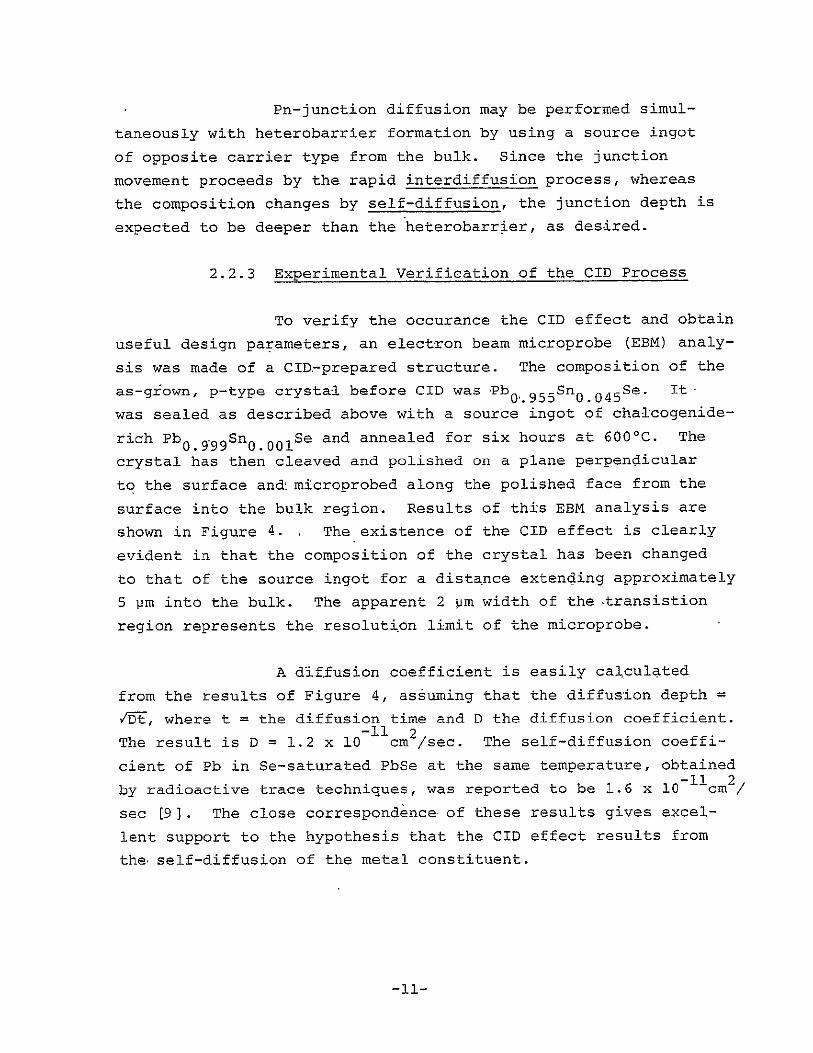

100
90
PbSe
801 region of SnSe outshydiffusion I
4-
4-I bulk
955 0 4 5 0o
20
SnSe 10
0 2 4 6 8 10 12 14
distance below surface (pm)
Figure 4 Composition vs distance into wafer for a Pb 955Sn 045Se
crystal interdiffused with Pb 0 9 9 9 Sn 0 0 0 1 Se at 6000C for 6
hours
Or P9
It is significant to note that the self-diffusion
coefficient of Pb in Pb-saturated PbSe is more than two ordersshy
of-magnitude less than that in Se-saturated PbSe Thus it is
expected that the heterobarrier depth in n-type material will be
much shallower than p-type
224 Lattice Matching Experiment
One aspect of heterostructure design to be conshy
sidered is the possibility of lattice mismatch between the layers
of different composition This may lead to strains and defects
within the crystal hence to device degradation Figure 5
shows the lattice constant variation for PblxSnxSe with
0 lt x lt 01 [1011] For the example of Figure 4 it may be
seen that the mismatch is less than 01 and even for Ax=0l
is only 016 From experience with III-V compound lasers [12]
mismatches of this magnitude would not be expected to be a problem
but the possibility cannot be overlooked
Attention was given to the potential lattice
mismatch problem in that a perfectly lattice matched structure
was fabricated This structure was achieved by utilizing the
fact that the two ternary systems Pbl xSnxSe and PblxSnxTe are
completely miscible over most of their composition range and
the addition of Te produces a larger lattice constant without
a significant change in bandgap This is illustrated in
Figure 6 which shows the lattice constant vs composition x y
for the quaternary system PblxSnxTelySey [1314] A large
range of perfectly lattice matched structures can be achieved In the work described here a PblxSnxTe ySey composition was
chosen to give emission near 12 pm and be perfectly lattice
matched to PbSe This composition was Pb096Sn0039Te0005Se0995
(as indicated in Table 1) and an ingot of this composition (G109)
was vapor grown The details of this lattice match are shown in
Figure 7 which is a blow-up of the lower right hand corner
of Figure 6 This crystal was interdiffused with PbSe to give
the lattice matched structure Point A represents the composition
-12shy
9 I613 -
1175CMEG
-o EG 810 cm
~E G =525 cm-1
= 612 U
611 0 02 04 06 08 01
x
Figure 5
Lattice constant (300K) of the Pb xSn xSe system for
0 lt x _ lt _ 01 E g values shown are at 12K
CM oO O
65LO If C3 L Pb Te
to0 64 - L
64 z
z Snco 62
0xwX 60
10 8 6 4 2 0
RPb- x SnxTe1y Se y
Figure 6 Lattice constant of the quaternary system PbJxSnxTel1ySey
showing iso-energy gap lines superimposed
6140 0
o IN
0610 0I-0C1
Co
0lt0
z 0 6120 X
_o 6110 Pb I Sn xTea S1yII-- - -
I-I
6100 1
010 005 0
Figure 7
Enlarged PbSe-corner of Figure 6 showing perfect lattice
matching between 12 pm quaternary material and pure PbSe
ORIGINAL PAGishyoF PoOR QUALUX
of ingot G109 while Point B represents the interdiffusediPbSe
region
Crystals of moderate size were grown from G109
Under microscopic examination large numbers of low-angle grain
boundaries were observed on the as-grown surfaces The cleavage
properties of the crystals were extremely poor and devices
fabricated from this did not exhibit laser action In view of
these poor initial results and NASAs expressed interest in obshy
taining high performance devices in a relatively short time
period this approach was not further pursued
23 Pn-Junction Diffusion
Pn-junction formation for this program was based on
control of stoichiometry deviations without the use of foreign
impurities For diffusion into p-type Pb1 -xSnxSe crystals the
vapor source was metal-saturated Pb1 -xSnxSe Movement of the
junction proceeds by interdiffusion which is generally orders
of magnitude faster than the self-diffusion mechanism governing
the CID process This difference in rates between the CID and
3unction diffusion processes makes it possible to control the
heterobarrier and pn-junction depths separately
Junction diffusions were carried out in evacuated
sealed quartz ampoules with the source ingot retained in an
inner quartz container to prevent physical contact with the -crystal Diffusion temperatures were in the range of 400o
600 0C and diffusion times from one to several hours Diffusion
depths were estimated from published values of interdiffusion
coefficients for the same condition [-9] In a number of cases
crystals were deliberately converted to opposite type using the
diffusion process Table 2 summarizes diffusion runs and conshy
versions carried as part of or in connection with this program
-13shy
Table 2 summarizes the diffusion runs and convershy
sions carried out in this program The original crystal growth
numbers are included as are performance characteristics of
lasers fabricated from these runs
OF
-14shy
Table 2
DIFFUSION RUN PARAMETERS
Growth
G No x-Value
95 0050
106 0047
138 0047
139 0030
142 0047
146 0047
156 0045
196 00445
D No
184
201
217
286
259
262
297
258
343
367
295
298
312
334
296
Diffusion
Type
Junction
Junction
Junction
Junction
Junction
Conversion
Junction
Junction
Conversion
Junction
Junction
Conversion
Junction
Junction
Junction
0 T(C) t(hr)
600 1
600 1
600 1
600 1
600 1
550 240
600 1
600 1
550 120
400 1
425 1
600 144
400 1
400 1
400 1
ORIGINAL PAGE IS OF POOR QUALITY
-15shy
30 DEVICE FABRICATION
31 Crystal Processing -
Following crystal growth useable facets were removed
by either slicing or cleaving Slicing was carried out with the
standard Laser Analytics procedure by use of a wire saw using
an abrasive slurry With proper use this method was found to
result in a minimum of crystal damage The cleaving method on
the other hand often leads to the introduction of crystal damage
most noticeable in the visible appearance of slip-lines along
[100] directions This latter method while considerably less
time-consuming than the slicing technique has therefore been
discontinued Wafers were typically sliced to thicknesses of
the order of 1 to 1-12 mm so as to allow enough material to
be subsequently removed to eliminate all saw damage Such saw
damage can propagate at least 1 or 2 orders of magnitude deeper
than the coarseness of the 5 pm grit used for cutting
32 Stripe Formation and Diffusion
After completion of the slicing operation the wafers
were ready for application of the insulator and definition of the
stripe pattern for formation of the stripe geometry junction
regions The general techniques for the formation of the stripes
involve evaporation of the insulator onto the wafer surface
through a metal mask which has a stripe pattern previously deshy
fined The resolution of this technique is more than adequate
to define 50 pm wide stripes (which has been a standard stripe
width at Laser Analytics)
After application of the diffusion mask the samples
were loaded immediately into a diffusion capsule together with
the diffusion source The capsules were evacuated sealed and
placed in the diffusion furnace
-16shy
33 Metallization
After diffusion the wafers were mounted with the
diffused side down and lapped and polished to a final thickness
of approximately 250 tim This procedure involved the use of
several slurry sizes each progressively finer than the preshy
vious one followed by a standard Laser Analytics final etching
The wafers were then loaded into the evaporator and metallized
with Au or CrAu on the p-side and In on the n-side Typical 0
metal thicknesses of 1000-2000A were used Cr was originally
contemplated because of its tendency to adsorb oxygen or oxides
and therefore provide a more tenacious metallurgical bond to the
Pb-salt material -This has in fact been verified and Cr
generally results in contact resistance values as low as those
observed for Au (typically 0005 to 0010 ohms corresponding - 6 2 to an RfA product of 1-2 x 10 ohm cm
A summary of the wafer processing operations carried
out to this point is given in Figure 8 After the final operashy
tion (step 6 in Figure 8) the wafers were cleaved into dice
34 End Face Cleaving
The metallized wafers were then mounted in special
cleaving fixtures and cleaved into individual laser dice A
photograph of the stations designed for wafer cleaving and die
mounting is shown in Figure 9 A schematic illustration of the
appearance of a laser die after this cleaving procedure is
shown in Figure 10 The laser dice were typically 14 mm
thick x 14 mm wide x 12 mm long
-17shy
WIES WCUTI AS-_GROWN FACET APPEARANCE OF WAFER AFTEARSAING OUTWFR GROWTH
P-N JUNCO
3CROSS SECTION OF WAFER SHOWING DIFFUSED REGIONS
5 FOLLOWING METALLIZATION OF THE JUNCTION SIDE
Figure 8
JDIFFUSION MATERIAL
2 APPEARANCE OF WAFER AFTER EVAPORATION OF DIFFUSION MASK MATERIAL
LAPPED SIDE
4 FOLLOWING WAFER LAPPING TO 250 UM THICKNESS
6 FOLLOWING METALLIZATION OF THE BACK SIDE
Summary of the wafer processing operations used in Pb-salt diode laser fabrication
OR1GINA pAGF 1
OF POOR QUALIT
U
I t
I I4 I I I il 1
S
Igt
i
ohmic contact insulator
heterolayer
pn junction substrate ohmic contact
Figure 10
Illustration of appearance of laser die after cleaving prior to package mounting
35 Die Mounting in Packages
The laser dice described in the previous section were
mounted with the striped side down on the copper laser stud
This provided for optimal thermal properties since the heat
generated near the shallow junction region was most readily reshy
moved in this manner The thermal resistance properties of this
configuration on the junction side can be obtained by reference
to Figure 11 The total thermal resistance 0T is given by
0T In + 0S
Where 0In is that due to the In metal contact (whose thickness
L is approximately 25 pm) and S is the spreading resistance into
the OFHC copper stud Assuming the thermal conductivity of indium
at 10K is 3 WcmK[15] and the contact area is 13 x 10- 3cm 2
the thermal resistance 0In = 07 KW The spreading resistance
term GS is given by [16]
0S = 2KM
where K is the thermal conductivity of the OFHC copper which is
approximately 5 WcmK and M is the linear dimension of one side
of the area approximately 14 mm Thus
0 ~ 5KW
The total expected thermal resistance of this configuration is
approximately 6 KW In practice this value has been found to
be of the order of 5-10 KW being influenced by thermal resisshy
tance values associated with the stud-to-package contacts as
well as the fact that actual laser dice are mounted at the edge
of the stud This model has also neglected heat removal from
the back side of the laser die but the calculated value is
nevertheless in general agreement with that observed in most
lasers
-18- ORIGINAL PAGE 18
OF POOR QUALITY
LASER DIE
- PN-JUNCTION
I N CONTACT AREA A
oFL45 13 x 10-3CM
OFHC COPPER STUD
Figure 11
Diagram illustrating thermal resistance calculation for diode lasers
I L2
I
Figure 12
SEM photograph of a typical laser die as mounted in the
the heat sink package The photograph was taken by
the NASA Langley Research Center
Dr John Buckley of
fMag = 45X
uOiGll4 pAGE 18)y p014 QUA
A photograph of a typical laser chip mounted in a
heat sink package is shown in Figure 12 This photograph taken
with an SEM [17] at a magnification of 45X shows the emitting
end of the laser pointing towards the right front The spongy
appearance of the top contact is due to the relatively thick In
plated on this electrode prior to laser assembly The small
overhang of the laser end over the sloped portion of the laser
stud is deliberate so as to prevent the shallow junction region
from being buried in the In plating on the top part of the stud
36 Experimental Package Studies
As a part of the overall objective of improving all
aspects of diode laser performance a preliminary investigation
was made into new methods of making electrical contact to the
laser dice Two new approaches werd considered 1) low temshy
perature soldering and 2) wire bonding
In the first approach lasers mounted in packages by
standard procedures were raised in temperature to slightly above
the melting point of indium (1551C) by placing them in a preshy
heated temperature controlled bath of purified stearic acid
After the melting step the lasers were cleaned in hot trichlorshy
ethylene and subjected to standard cleaving procedures Fiye
different devices were fabricated by the technique In every
case the electrical characteristics remained essentially unshy
changed but laser action was completely quenched It was apshy
parent that this heating process introduced crystalline strains
in the die which quenched laser action While lower temperature
solders are available previous results have indicated that they
either do not have the desirable wetting properties of In or
exist in a two-phase form which segregates in the small quantishy
ties involved in laser fabrication
-19shy
The second approach was a wire-bond technique using
a 0003 diameter gold wire soldered to a shortened top electrode
and pressure-contacted to the laser die It was felt that this
contact would remove the major contact induced strains in the
crystal Pressure was applied with controlled weights on a
piston fixture After several optimization attempts a laser
was successfully fabricated by this technique and delivered to
NASA Langley ResearchCenter (Serial No 6271-3) However the
contact failed during operation and the laser was subsequently
replaced We believe this method has promise but will require
the use of specialized die-bonding equipment and considerable
development time to effect
-20shy
40 LASER EVALUATION
41 Evaluation Methods
411 Dip Stick Testing for Electrical Characterization
The electrical characteristics of the diode lasers
were studied by pltting the I-V curves using a 4-point probe
technique designed to eliminate lead resistance effects The lasers
were mounted in an evacuated dip stick which could be immersed in
a liquid helium reservoir A GeCu infrared detector mounted in
the dipstick made it possible to measure the threshold current
of the laser and obtain an estimate of theoutput power
As an illustration-of the technique a typical
I-V curve of a high performance Pb09555Sn 0445Se CID device is
shown in Figure 3 (This laser was fabricated from crystal G196)
This I-V curve exhibits the slope discontinuity at threshold which
is typical for high performance Pb-salt lasers and indicative of
high internal quantum efficiency [18] The value of the voltage
intercept as shown in Figure 13 is 1045 mV (corresponding to
842 cm- ) in reasonable agreement with the laser threshold freshy-quency of826 cm I observed during subsequent optical testing of
the laser emission More information on the optical charactershy
istics of this device is given in the following section
A photograph of the dipstick test area is shown
in Figure 14 The dipsticks are evacuated after laser mounting
using the cryopumps shown in the figure The test arrangement
is such that 2 lasers can be mounted in each dipstick These
-21shy
__
__________
OF pOOR QUALITYORIG~hIAL PAGE IS
-Fshy
+ _I_ _____ --- -- --- ______ _ _ _ __--
-K - __ -__ __ __ ____-__
- - r I Elctial carceri cs of r----f I F -- ___
- -- -I pa---- -i--- 1K th st aAg t l n ---- =___-_-- - -shy
curv extrapolates ____ _ ono th
t 1 t _ ____
he sjar___
fige ure 13raoats E _ ___ __ __ _c _ -- _ _ x __I
an ____zrEh~zto 104SmV corresponding to _
F- iexpected laser emission of
42 cm nearthreshold -- shy
2D_
________ _________ _- t n~ g t l n o -
t__-- thIta E 1 K _
___ tio urve extapolates ___ 1_v__f 72lfl ___of the - - - - - -=-_
- --- cresodigtoato14m t
II p
IA
I I i I-I
La
e
Tig
ure 14
Laser
Dip
sti k
Testin
g
Area
dipsticks also proved useful for the thermal cycling tests
(described later) since the lasers are located in a vacuum enshy
closure and are therefore protected from moisture condensation
412 Evaluation of Emission Characteristics
The diode lasers fabricated during this program
were studied for a variety of optical performance characteristics
including
Threshold current vs temperature
Output power vs temperature
Spectral distribution vs temperature
Output power vs current
Limited measurements of tuning rate far-field spatial output
distribution and noise were also carried out
4121 Spectral Characteristics
The system used for the majority of
these measurements is diagrammed in Figure 15 The lasers were
mounted in a Laser Analytics Model TCR Stable Temperature Closed
Cycle Refrigerator which allows temperatures to be varied from
10K up to room temperature The collecting element was a corshy
rected fl KRS-5 lens with microadjustment Laser mode charactershy
istics were measured with a 12 meter grating monochromator and
the radiation was detected with a cooled HgCdTe infrared detector
The power output was measured with a 1-cm diameter pyroelectric
detector which could be shifted into the optical path
behind the chopper using a mirror arrangement The power meter
was supplied by the National Bureau of Standards Boulder Colorado
The lasers were powered by a Laser Analytics Model LCM Laser
-22shy
DETECTOR INFRARED LOCK-IN CRYOGENIC BIAS DETECTOR AM
TEMPERATURE X- _ STABILIZER RECORDEI
R LECTOR LENS
POWER CRO METERL RASE A GRATING
COOLE iMONOCHROMATORKRS-5
F1 CHOPPER DRUM LENS
SLASER CONTROL
MODULE
Figure 15
Schematic diagram of equipment used for evaluating optical
characteristics of diode lasers fabricated during the
program
Control Module The output of the system was displayed on both
an oscilloscope and an XY-recorder
As an exaEmple of the spectral measureshy
ments carried out during this program the spectral charactershy
istics observed from laser -7075-12 discussed in the previous section
are shown in Figure 16 The threshold frequency of this laser
-is 826 cm in close agreement with that obtained from the zeroshy
current intercept of the extrapolated value of the linear portion
of the I-V characteristics This laser had a maximum CW output
power of 105 mW per end at 127K At 20K the laser ran single
mode with an output power of 088 mW
4122 Spatial Profile Measurement
An Amperex pyroelectric vidicon was
used for preliminary measurements of the spatial distribution
The vidicon sensitivity is such that when the far field pattern
is spread over 50 of its receiving surface it can sense about
50 i-watts of infrared power The laser utilized for-this preshy
liminary experiment was a Pb0 97Sn0 03Se CID device from Laser
Analytics stock The laser was operated in a square wave mode
to provide the required AC signal Results obtained in this
manner are shown in Figure 17 The photograph of the CRT was
taken as the vidicon was slowly moved across the optical path
This mode of operation enhances the display contrast but care
must be taken to interpret this data Adjacent regions of dark
and bright areas correspond to regions of radiation intensity
the bright areas corresponding to the leading edge of travel (the
heating period) and the dark areas corresponding to the trailing
-23shy
LASER ANALYTICS INC 38 HARTWELL AVE
Grating SU Factor )79o Order2 Teperature Sensor -i3 0 LEXINGTON MASS 02173 I ------- bull
- I I shy=
- - = AIthP A
I --- - Ii - ----shy-
I - - (
T
S-------------
1 TIth~- -- --
---
-
-----------
-----shy
---
T 7
T--IIUthh~shy --plusmn - -
-----= I I -A
--- -shy - --shy
------- -------- T- =1_ i--------------T
S T - - = --- uL -7 lt - -------shy
7 1 - - I
9797- -fj 3 ii 1 I
th QFigure 16 th
Mode structure of laser 7075- - I = [ i ------------
--
C12 at 10K 20OK 40K 60K and 75K All spectra were taken - ---------------shyat 2 amps ------r------------shy
Atlt 4
NOR f 1 M Arl-
or n p
Tu44gt
TAW4
4 isVih
iA
0 All
11 4i
I r5 Iamp
+ 4 Ptnira 1
Wri1 ataat10pW 0 agt9 zcar
M4o
)4t 4
44A~ 17 gt~ 444 4
The small bright spot on the right edge (the cooling period)
half of the photograph was due to an imperfection on the vidicon
surface
An important aspect of this experiment
is that concentricrings due to diffraction effects associated
with the refrigerator window nearly mask the laser beam pattern
This result corroborates earlier measurements made by scanning
detector techniques Similar patterns have been reported for
GaAs lasers beamed through external diffraction structures [191
Circumvention of window effects to achieve a reliable measurement
of the spatial pattern would require the use of wedged windows
with anti-relfection coatings Time and cost restraints prevented
the enactment of these remedies hence these measurements were
not further pursued
42 Electrical and Optical Performance Results of Lasers
Delivered to NASA Langley Research Center
A total of nine lasers were delivered to NASA Langley
Research Center during this program Each of the following sections
contains the following information for each laser delivered
(a) I-V characteristics at lOK and 77K
(b) Emission spectra at various temperatures and at
2 amps
(c) Tables summarizing the variation of threshold
current output power (2A) and output frequency
(2A)
-24shy
421 Laser No 7028-6
(a) Electrical characteristics (Figure 18)
(b) Spectral data (Figure 19)
(c) Table of Ith Pout and frequency vs
temperature (Table 3)
-25shy
___
oRIBINAL PAGE JS OF POOR QUALITY
7028-6Laser No 0 3x = 0
R = 005 ohms
IFshy
_ _ __ =shy_ __-_ _ _
------ shy---- - - _ -
_t- I -I -shy
__ Ft ---= _ iv___ ~~~__ _ - - __
El crcl hrceristics
- r--r77K _---shy__ _
7Z 77K 7
--
LASER ANAL CS INC 38 HARTWELL AVE
Grating__- - Factor 896 Order I Temperature Sensor 2 5 LEXINGTON MASS 02173 I JU- - JL -I----iI- F F -- =
=I -I-J I -- I-- - - F0 shyt III ILL-II I L j hZth~C C shyt__j _Lplusmn_LI iLWJ - ---I
-IJ miP-I =oq-JjI 4-LLt~z-Utb- - --=oWh- -- L i - IH - --L L iD 6 IPJl Ill shy- P 3 r I-0Hq37i~itIflh1S7L1i41
-~Lwvt-iII 1 1]li~tt LF7 gt_- -- shy1 +4=t I_ _iJL I- -- --
I- I I [IFjIE_II da
I--- III - __~j- ltIII-- I LIwI--J--I---- t III L 1 ~ j t
T tI - J- IhI tI t
ltL- - 11 -LHPltE--_____-__1 1IIIIHIHiA9 plusmn_L plusmn1 -LL plusmn1I-Ph -L - - _ - -1 d-
-iI --- - - -L j I-I
i_ _+I_ +__ Iplusmn_IE_ V_ i-p- ___--_j --_ - -T
FMI-ki i I In ----- I_- + -- j- -H5-l- shy ---- ---- = - --iT- I -I J-1+ II ___riIILL
-i---------- II t ItH --- i tth21 -lit r ]j = IT - ---
- _
-II--I- HL
Figure 19 --- ----- -- Spectral output vs 0 ra- I -_shy
temperature for laser 70286ili - - -- c I -T t-l--r-l
I
Table 3
SUMMARY OF OPTICAL DATA FOR LASER 7028-6
2-Amp2-AMpSingleEndedOutputFrequencySingle-EndedLaser Package CW OutputIthTemperature Range (cm
(K) (mA) Power (mW)
867- 952043962010
961- 978035161020
1049l1060026357740
1150-1155007060060
OPIGINAL PAGE 18
OF PO1R QUALITY
422 Laser No 6271-2
(a) Electrical characteristics (Figure 20)
(b) Spectral data (Figure 21)
(c) Table of Ith Pout and frequency vs
temperature (Table 4)
-26shy
ORIGINALPAE1 OpPBOOR QUALMT
~~ aer No- 6271-2
000 5
H ohm
f R 03
R HI
~~~~~~~~~~~~~~~~~~~~~
shy r--n-rr+amp-
laser
+ 4 Eectrcalharateriticsof-shy
6212t10nd7K
2o 4o61
LASER ANALWIS INC 38 HARTWELL AVE
Grating _ p
Factcr Order Temperature Sensor 3 go LEXINGTON MASS 02173
----- - - - -shy
3[t l [ th--- ---
- i---- tW -t---- - - - - t
T+- P i
--
449
Q -T
i P-H -i-H
t - --
H I------I=
T o( S
- -------------
T -1-I ITT---
D4 it
- = --
- -shy-
1- In
IL I-- E-1T--
igure 21 h tth
temperature
P = Spectral output vs for laser op r t n62712
P =
Table 4
SUMMARY OF OPTICAL DATA FOR LASER 6271-2
2-Amp- output2-AmpSigl-Ende Laser Package Single-Ended Frequency Temperature th CW Output -I
(K) (mA) Power (mW) Range (cm
10 400 0132 727-741
20 490 0105 735-746
40 840 0088 776-788
-60 1540 ~002 851-860
65 1900 -001 875-877
O IJ
423 Laser No 7067-5
(a) Electrical characteristics (Figure 22)
(b) Spectral data (Figure 23)
(c) Table of Ith Pout and frequency vs
temperature (Table 5)
-27shy
--
--
ORIGINAL PAGE I8 OF POOR QUALIY
Laser No 7067-5
x = 00445
Sf= 00145 ohms
_QCshy
- _---__I
_ __
Figure 22
Electrical characteritc of laser 6067-5 at 10K-and 77K
Syj Zo6 -o )O
- --- ----- - -
LASER ANA4 CS INC HARTWELLAVEL 38X G
5 7-O Order Temperature Sensor _ L NGTON_MASS 0217 3 Grating Factor
-plusmn = o4 kK - S ATELAEKt~ l it tKqi-- - -
Ii4 i--1 - - - I _ - ------- t ---- - -shy
t h I--I- --- - U----
TflTI I4- I Ishy
-- i 1 - ----- --I-IP A
- -th=th th
IL 2 --- -shyt- HP-----
S_ THI
Ii - I -Ht F L-JL - _ ~ t - --th ---shy
] I -plusmn- Iplusmn i 7J +F- 2 I~~
t- igur 2= - - -Jdc-th -I- --
- HutuiSecrl oeatn -S mj 4l_r____- Hii[-ITi
PFigure 231=~~~~- IAi-tWLplusmn - ~i --- ---- Specal output vs operating LIt LWUlterperature for laser 7067-5 - I-iT jFI + - - tI I - -- 1iI ---- --
I HII I I 111111 I ___ L-------iI 11
Table 5
SUMMARY OF OPTICAL DATA FOR LASER 7067-5
2-Amp2-AmpSingleEndedOutputFrequencySingle-EndedLaser Package CW Output1thTemperature shy
(K) (mA) Power (mW) Range (cm I
841-85305060010
909002190048
1S0910GE op QIJMS1
424 Laser No 7067-7
(a) Electrical characteristics (Figure 24)
(b) Spectral data (Figure 25)
(c) Table of Ith Pout and Frequency
vs Temperature (Table 6)
-28shy
OIGINAL PAGE IS
OF POOR QUALITY
Laser No 7067-7
x = 00445
RF- 0023 ohms
- -
d
nFigure 24
_ Electrical characteristics -- of laser 7067-7 at 10K and
It _ - - - -
[6 20dego
LASER ANAYtCS INC 38 HARTWELL AVE
Grating
F actor 7 Order
-- T =
Temperature Sensor
T
lj
- --
LEXINGTON MASS 02173 I
-
th -L- - --- 2t
]th t[j ~ i- 1 -l--H - - - 4 -
_=-h0 - IV
jiP tti--yiplusmn
4 t
th -shy
t 2 gt7J-- --- -
ll- tt ----shy w t jj i I = = - -I-
~- - - ------ --
th
-
p8V
---
_
-
I~L I I =-
I -m-r-shy-L---HT- I=
- --I i
_1-t4 ij_hlIth -
-z
--shy [7
I
-t
- h
F-
- I1 4
1ttt
SS e ta oup t v-pe a i g i __ --I I -
P7 te pe at r fo_ l s 7067 7T= -H+FI I - I I gt 7 lt 1 II ilL I~~L +-I
71771rI- u _ t
T - shy---
------shy
----shy-- 1
Spectral output vs operating temperature for laser 7067-7 -
- plusmn P1 -
i-i -1----i-----I--- E---shy
Table 6
SUMMARY OF OPTICAL DATA FOR LASER 7067-7
2-Amp 2-Amp Output
Laser Package Single-Ended Frequency Temperature th CW -otput
(K) (mA) Power (mW) Range (cm
10 800 0246 834-860
20 860 0175 846-864
36 1480 002 895
ORIGINAL PAGE I1 OF POOR QUALITY
425 Laser No 7075-12
(a) Electrical characteristics (Figure 26)
(b) Spectral data (Figure 27)
(c) Table of Ith Pout and Frequency vs
Temperature (Table 7)
-29shy
OF pouh R
Laser 7075-12
x 00445
Rf 0025
_I 4
I I
26 Figure
CharacteristicsElectrical of laser 7075-12 at
10K and
77K
02D404QA CteAI
LASER ANAI1t S INC - 38 HARTWELL AVE
LEXINGTON MASS 02173pGrating 4 Factor T7B rder r TemperatureSensor Q3amp0
- -t -- aco - - rd - 2v
T T 7 T
- P
~ itIhI th=lg
1rI 2 - th =th=shy
-t -- -- shy Ltemperature-for p-+-- taserW7075-12
Ill(DT
Spectral output vs operatingr -shytemperature for laser 7075-12 P
Table 7
SUMMARY OF OPTICAL DATA FOR LASER 7075-12
Laser Package Temperature
(K)
10
20
40
60
75
th (mA)
440
480
820
1260
1850
2-AmpSigl-Ende Single-Ended CW output Power (mW)
105
0877
0263
0175
002
2-AmpOutput Frequency
Range (cm
826-829
832
874-884
947-949
1011
ORIGImNAL PAGE IS OF POOR QuALfij
426 Laser No 7109-6
Cal Electrical characteristics (Figure 28)
Cb) Spectral data (Figure 29)
(c) Table of Ith Pout and Frequency vs
Temperature (Table 8)
-30shy
ORIGINAT PAGE IS OF POOR QUJALITY
H-1 Laser 7109-6
i 700445
Hf o02 ohms
v
k
Elecrica
Chractrisics
t
Et
HH
I p
20L
--
D LASER ANAgt25 INC 38 HARTWELL AVE
Grating A Factor4 deg Order Temperature Sensor 3 ( LEXINGTON MASS 02173
T T= S- T =
Ith =QIth = (DmI = I =
6-1
-SP --
-I~II
T T
-T 4-1 1
I - F9
T shy-- IILI ____
- - - - - - - - - s -bull - P- N rtinh I- J ------ t h-shy h -MI I it
=
I Fiur 29SetaOuptV-tprt 4tIl-QwV tepeatr for~ laserI- 7109--- --shyi~ -- -I~~~~~- 3~t sect k
T= I -I- I-- - r -shy -- j-
Table 8
SUMMARY OF OPTICAL DATA FOR LASER 7109-6
2-Amp
Laser Package Temperature
(K)
th (mA)
Sg2-Amp Single-Ended CW Output Power (mW)
output Frequency
-1 Range (cm
10 590 0570 812-864
20 690 0526 852
30 1100 0044 869
32 1900 002 869-890
ORIGINAL PAGE IS OF POOR QUAITY
427 Laser No 7111-3
(a) Electrical characteristics (Figure 30)
(b) Spectral data (Figure 31)
(c) Table of Ith Pout and Frequency vs
Temperature (table 9)
-31shy
Laser No 7111-3
=T-= x = 00445
Rf= 00135 ohms
E e
t
i
a
S
~z
ri
E
H rr
r -
I
-
rr
- I
i
P k
70
ORGIA
01
PAGE
0
is
le
II ORGIA PIG lOOR 1
__
---------
-- --
-LASER ANAUS IN(38 HARTWELL AVE
LEXINGTON MASS 02173 Grating _Factor 8c6 Order Temperature SensorjikZZ 1-1 T = T T
th i- (E
P PO -
- -y i=i=D 1 ith
--- - - - - -IT-
tI-- shy
- -- t--I--------
tt~I -t
-- - - -
th---
-1--~~x -- - -r
v -- i-S pu - t
-+) 1 0r--r-
1-empert fo- l
t 88+8 oo+cflamp__
-N
Table 9
SUMMARY OF OPTICAL DATA FOR LASER 7111-3
2-Amp
Laser Package Temperature(K)
Ith(mA)
2Am Single-EndedCW OutputPower (mW)
Output Frequency-1Range (cm
10 1400 0263 820-831
20 1700 0263 829-838
40 1880 003 888-895
Oolt
428 Laser No 7061-1
(a) Electrical characteristics (Figure 32)
(b) Spectral data (Figure 33)
(c) Table of Ith POut and Frequency vs
Temperature (Table 10)
-32shy
II
ORIGINAL PAGE IS OF POOR QUALITY
_- __=___
xo047 _ _~_________-- -r_~~Rf 0022 ohms -
FEshy
= ~~~~~-- u--- _Lf__f-i_
_
4- L-
IrIshy
~~Figure 32 +kshy
~Electrical characteristics _ __
H of laser -7061-1 at 10K and
- 77K _- _ -shy
-i ----shy I
-- -
-------- -
----- -- - -
i
LASER ANALYTICS 38 HARTWELL AVE
INC
Gtalting (Sp- Factor Order I Temperature Sensor 9ampoR SLWS 20 LEXINGTON MASS 02173
T -L--------
Iiit+L= ---
LL1- -T-0--f - -shyz
Il -----
tt -
-3
H(DAL
- --- hI 1-1 21 i~ --------
IIt
IiK 1 I7-I7 -11 + - [+L3 T I - i
1-i-I--l4 Tth = H 215-i L1I
-Ii----------------P
I L o
T ------ -=--shy
-- - I--------- 0 3
]E -ll -i F- -i--T S e t a ou p t v ng
Itemperature for laser 7061shybull - ---i -- --- -------- _-A4i--------shy7-~~---- 4 --- -----I--
Table 10
SUMMARY OF OPTICAL DATA FOR LASER NO 7061-1
Laser Package Temperature
(K)
10
20
40
60
80
95
th
(mA)
148
158
200
333
680
1520
2-Amp2-AmpSingle-Ended CW Output
Power (mW)
07
07
07
08
06
01
Output Frequency
- IRange (cm 1
770-796
780-800
825-851
894-906
974-1006
1045-1051
429 Laser No 7069-1
(a) Electrical characteristics (Figure 34)
(b) Spectral data (Figure 35)
(c) Table of Ithm Pout and Frequency vs
Temperature (Table 11)
-33shy
_____
----
__
- _I ------
1 _ 7069-r _ Laser
x 0047 1 -- +-shy
f 0027 ohms
t_L___________________-____=Eshy ___
-I -I
_shy- -- H- --~-
7__1_ _ 1L - -- -E
_-_-- ME INshy
_ _
4+- shy_ _- _--
_ - _--
- gt
-- shy 34~~~~Figure
~~Electrical characteristics--i
anoflaser 7069-1 at 10 and-
10
77K
1t0RoeuroT
LASER ANALY ILCS INC 38 HARTWELL AVE
Grating I ) 6f7)Order Teperature Sensor 9 9 LEXINGTON MASS 02173LA-Factor I -- -I -
----- ------ 0 th-n-- yF--- -- - - - - - - --o - - -~ w i-
_th-I = 2t j -v th 3 I= P Ca
iI-I- I - I-------------------]
Th- _z ~I
- -- output iLLL- - - ---peer
VV
----------------------- I ---- 11 x
--shy
0MIshy
th H - - t-ishy
fF- I rplusmn
-11-t -V -I-j -
-----------------
IthH
-1 J-~f T1- Fiur 35 [ 11 ---- Spectral output operatnshy----- vs
-- temperature for laser 7069- --shy
j-4-1- shy
-i
Table i
SUMMARY OF OPTICAL DATA FOR LASER NO 7Q69-
Laser Package
Temperature (K)
10
20
40
60
80
Ith (mA)
122
135
190
332
709
2-AmpSingle-Ended
CW Output Power (mW)
009
009
013
009
-002
2-AmpOutput
-u Range (cm
771-797
782-802
833-849
927-1006
1052-1089
ORIGINAL pAGE IS
OF poop QUALITY
43 Summary and Discussion of Laser Performance Data
Important operating characteristics are summarized in
Table 12 for the lasers whose properties are given in Section 43
above and for two additional devices discussed in the next secshy
tion The following observations are significant
1) Four out of the twelve lasers in Table 12 had CW
operating temperatures above the boiling point of liquid nitrogen
2) Eight out of the twelve- lasers had CW operating
tepperatures in excess of 60K
3) Five of the lasers in Table 12 had CW singleshy
ended power outputs greater than 05 milliwatts
4) Four out of the twelve lasers exibited single mode
CW single-ended power in excess of 05 milliwatts
5) CW operation above liquid nitrogen temperature has
been achieved at wavelengths as long as 1035 pm (the longest
wavelength previously peported for operation of any diode laser
at 77K or above is 96 pm [19] 1
These results represent a substantial improvement in
the state-of-the-art of tunable diode lasers in the 8-15 pm specshy
tral range Previous homojunction lasers -in this range have
generally had maximum operating temperatures below 40K have
never exhibited 77K operation and have consistently produced
maximum CW power outputs of less than 05 milliwatts overall
The CID technology can now be used on a reproducible basis in
both the PbSSe and the PbSnSe systems
The results of the present progtam show that the CID
technology can be used to provide significantly improved pershy
formance on a reproducible basis throughout the 8-15 pm range
-34shy
Table 12
PERFORMANCE CHARACTERISTICS SUMMARY FOR LASERS
PREPARED AND EVALUATED DURING THE PROGRAM
Maximum Maximum CW Single Tuning
Crystal Junction Date Operating Ended Power Range Laser Growth Diffusion Delivered to Temperature Output R -I
x-Value No NASALangley (K) (mW) at T(K) (cmSerial No Run No
6271-2 95 05 184 32377- 65 01 12 726827
6271-3 95 05 184 32377-1-1- 60 01 720-864
726-9666313-3 106 047 201 85 04
1 6315-2 106 047 201 - 85 12 800-1051
7028-6 139 03 258 2277 60 04 13 867-115460 766-1051286 61577 95 08
7061-1 106 047 7067-1 196 0445 296 32377 48 05 13 841-853
7067-7 196 0445 296 32377 36 02 13 834-895
7069-1 138 047 297 61577 80 01 40 742-1089
7075-12 196 0445 296 32377 75 10 13 826r1011
7109-6 196 0445 296 42577 32 06 13 812-883
7111-3 156 045 334 42577 40 03 20 820-895
1 Returned for repair due to single strand lead wire fracture Returned aftertepair
It This laser fabricated in an experimental wire-contact configuration failed at NASALangley
and was returned to LAI
This x-value indicates the material composition Pb1 xSnxSe
Not delivered Used in reliabilitylifetime studies described in Section 45
This is the temperature at which the laser output power decreased to approximately 0009 pW
44 Reliability and Lifetime Studies
A number of failure and degradation mechanisms were
observed and addressed during the course of this program The
following paragraphs discuss these problems and solutions which
have been developed
441 Package Relaxation
During this and other Laser Analytics programs
it was found that a number of lasers exhibited a pronounced inshy
crease in series resistance after a few temperature cyclings beshy
tween room and cryogenic temperatures It was discovered that
the effort resulted from the relaxation of laser package parts
which had been strained at initial assembly This problem was
overcome by straightforward design modifications involving addishy
tion of a second set-screw Figure 36 shows a demonstration of
cycling behavior in which a laser was cycled from 300K to 77K
twenty times-with no change in electrical characteristics
442 Crystal Degradation
The term crystal degradation refers to a failure
mode apparently associated with the laser crystal or its deposited
metal layers rather than the package As an example Laser No
7061-1 was stored at room temperature and shipped more than four
months after initial assembly its electrical characteristics at
the time of shipping were given in Figure 32 Figure 37 shows
the electrical characteristics on the date of assembly for comshy
parison It is apparent that during the four-month storage
period the series resistance increased from 6 milliohms to
22 milliohms and the threshold current from 0110 amps to
-
0455 amps
-36shy
OtIGINAL PAGE IS OF POOR QUALITY
As another example Laser No 6313-3 had a
series resistance of 10 milliohms and threshold current of
082 amps at assembly After three months the series resisshy
tance increased to 61 milliohms but the threshold current deshy
creased to 060 amps This threshold reduction dan be related
to a decrease in a pronounced excess current near zero bias
The excess current is thought to be related to surface effects which become less pronounced with time This laser was subseshy
quently destroyed in an attempt to re-seat it in the package
As a third and extreme example Laser No
6315-2 completely failed within a time of one month
443 Low Temperature Storage and Operation
Three high performance CID devices were stored
in liquid nitrogen for varying periods of time Results are
shown in Table 13 The conclusion can be made that negligible
degradation occurs during cryogenic storage
Qualitative observations at our laboratory and
by a number of purchasers of Laser Analytics lasers leads to
the conclusion that high performancePb-salt-lasers do-not deshy
grade for-indefinitely long periods of operation as long as
they are maintained at cryogenic temperature
444 Discussion
Lifetime and reliability problems have in the
past been confused by a combination of effects occurring simulshy
taneously It now seems clear however that a crystal degrashy
dation problem does exist in Pb-salt heterojunction devices
The effect is much more pronounced in MBE and LPE heterojuncshy
tions but is also significant in CID A report on this subject
-37shy
Table 13
LIFETIME STUDIES OF HIGH PERFORMANCE PblxSnxSe CID LASERS
STORED AT LIQUID NITROGEN TEMPERATURE
Rf (42K)Ith (42K)Storage Time (amps) (milliohms)
Laser at 77K After After Serial No x-Value (Months) Initial Storage Initial Storage Comments
76315-1 0047 3 046 046 80 80
7068-1 0030 3 046 052 90 110 Increased Ith related to increased excess current
7068-2 0030 2 038 036 170 170 Decreased Ith related to decreased excess current
-with recommendation for action has been submitted to NASA by
Laser Analytics [21]
Since the effect is most pronounced with heteroshy
junctions it is likely to be associated with lattice mismatching
Thus one solution may be to further perfect the quaternary
growth procedures discussed previously Alternatively an opshy
timization of the degree of lattice mismatch may be possible
the tradeoff would be the height of the heterobarrier
Finally if a short range solution should not
be feasible a practical fall-back position is to maintain the
lasers at or below liquid nitrogen temperature continually
-39shy
-4-4-4
+ -r r4 t
tli1m fi
V4M
C ti LIM fIN Tl ZfK
-----------
ORIGINAL PAGE IS OF POOR QUALITY -
9 ---0 -- --- 1 - -F- - - -- -shy
-oo - - --- I 1 - - + - _ _- -+ = a--- - -- = - i--t--- -t - k -_ + _
t i - I -
r - t =
1 -
- r--+ - EZ--- r - - ----I - - - --- F h--zshy
Io- shy
r - 7_- 1 at- t -
-- - I t J ti i i [V]
time of fabricat ion
--- - -
--- --
50 CONCLUSIONS AND RECOMMENDATIONS FOR FURTHER WORK
51 Results
The central result of this program is that theCID
Technique has been successfully applied to produce single heteroshy
junction Pb-salt diode lasers with significantly improved pershy
formance Single-modeCW power outputs as high as -05 milliwatts
have been achieved at an operating temperature of 20K and CW
operationabove 77K has been obtained for wavelengths as long
as 1036 pm Ten laserswere delivered to NASA under the conshy
tract of which two operated CW above 77K and seven above 60K
Two additional lasers operating above 77K were fabricated and
used in reliabilitylifetime studies These results represent
a significant advance over earlier homojunction methods which
typically result in maximum attainable single mode CW power
nilliwatts and maximum operating temperaturesmuch less than 01
less than 40K
Contact degradation manifested by increased series reshy
sistance and consequentialperformance degradation was noted
and explored Significant progress was made in definingthe -
effect Astop-gap solution to degradation problemswas found
to be storage at liquid nitrogen temperature
5-2 Recommendations
Continued work with CID structures should include a
systematic study of both pn-junction and heterobarrier diffusion
properties At the present time the carrier confinement width
is only qualitatively known or controllable An improved strucshy
ture with confinement widths of less than 1 pm may result in
very substantial improvements in both output power and operating
temperature In addition to an improved confinement structure
control of junction and barrier depths will allow optimization
of junction depth with regard to thermal properties Pn-junction
-40shy
diffusion depths can be measured by angle-lapping and probing
techniques Heterobarrier depths require an EMB system for efshy
fective measurement
Investigations into reducing the barrier height differshy
entialby using a more closely matched x-value in the CID difshy
fusion source may reduce lattice mismatch problems andimprove
room temperature storage properties Alternatively further
research into quaternary compound formation may result in zero
lattice mismatch
The sublimed binary experiment indicated that crystal
growth procedures are not optimum and that new purification
techniques may result in greatly improved crystal quality
It is strongly recommended that a systematic investishy
gation into reliability and lifetime questions be immediately
instituted and vigorously pursued
Noise properties of diode lasers areimperfectly
characterized and not well understood A systematic investigashy
tion of noise and instabilities in tunable diode lasers would be
of considerable value
Preliminary investigations of liquid phase epitaxy
(LPE) have indicated high performance devices can be obtained
While reliability and yield problems presently dominate this
technology future efforts aimed at obtaining a better undershy
standing of these phenomena are indicated For the long range
double heterostructures are expected to result in devices subshy
stantially better than single heterostructures
The above recommendations are believed to be of parshy
ticular importance as a result of the findings of the present
program Other important areas to pursue include 1) improvement
ORIGJINA pAGFI 1S - 4O QUAUW
of contact metallization procedures 2) new packaging techniques
3) stripe-width optimization 4) development of anti-reflection
coatings and 5) investigation of controlled doping by foreign
impurities
-42shy
60 REFERENCES
1 KJ Linden KW Nill and JF Butler IEEE Journal of
Quantum Electronics August 1977 (to be published)
2 AR Calawa TC Harman M Finn and P Youtz Trans AIME
242 374 (1968)
3 TC Harman and Ivars Melngailis Applied Solid State
Science R Wolfe editor Academic Press New York
(1974)
4 TC Harman and JP McVittie Jour Electronic Materials
3 843 (1974)
5 SH Groves KW Nill and AJ Strauss Appl Phys Lett
25 331 (197-4)
6 JN Walpole AR Calawa TC Harman and SH Groves
Appl Phys Lett 2-8 552 (1976)
7 JN Walpole private communication
8 KW Nill and SH Groves private communication
9 RW Broderson JN Walpole and AR Calawa J Appi
Phys 41 1484 (1970)
10 S Yamamoto Science Reports Tohoku University 40 11 (1956)
11 M Neuberger IV-VI Ternary Semiconducting Compound Data
Tables EPIC-S16 p- 22 March (1976)
12 MH Pilkuhn and H Rupprecht J Appl Phys 38 5 (1967)
-43shy
13 CA Kennedy and KJ Linden J Appl Phys 41 252 (1970)
14 L Laugier J Cadoz M Faure and M Moulin J Crystal
Growth 21 235 (1974)
15 R Radebaugh Rev Sci Instr 48 93 (1977)
16 R Scapple Sol State Tech 74 April (1974)
17 SEM photos were taken by Dr John Buckley of the NASA
Langley Research Center
18 JN Walpole AR Calawa RW Ralston TC Harman and
JP McVittie Appl Phys Lett 23 620 (1973)
19 i Hayashi Appl Phys 5 25 (1974)
20 ED Hinkley RTKu KW Nill and JF Butler Appl
Optics 15 1653 (1976)
21 Laser Analytics -ReportLAI 77-2-9 February 15 1977
-44shy
APPENDIX A
A portion of the results of this program was included in the
following article
Single Heterostructure Lasers of PbS lxSex and Pbl1 x
Sn Se With Wide Tunabilityx
K J Linden K W Nil and J F Butler
Journal of Quantum Electronics (to be published in
August 1977)
720 IEEE JOURNAL OF QUANTUM ELECTRONICS VOL QE-13 NO 8 AUGUST 1977
Single Heterostructure Lasers of PbSl-xSex and Pbl-xSnxSe with Wide Tunability
K J LINDEN MEMBER IEEE K WNILL MEMBER IEEE AND J F BUTLER SENIOR MEMBER IEEE
Abstrcr-Single-heterostrueture diode lasers formed by composi-tional interdiffusion in PbS_xSe and Pb1 xSnxSe and by liquidshyphase-epitaxy (LPE) in Pbl SnSe show performance characteristics _ significantly better than those observed in conventional homostmeture lasers Higher operating temperatures were obtained for all composi-
tions with CW operation above 77 K being achieved for compositions corresponding to wavelengths from 41 to 127 Arm Single-ended CW powers as high as 70 oW corresponding to lext = 44 percent were ob-served in PbSi _Se devices
I INTRODUCTION
T HE TERNARY Pb-salt semiconductors Pb1-CdS PbS-Se- and Pb-xSnSe provide tunable diode lasers0
throughout the infrared region of 3-30 pm These lasers are finding a growing use in spectroscopy-related applications where they provide measurement capability far beyond that of conventional instruments In spectral absorption studies for
example they allow measurements with a resolution better than 10 4 -cm which is many orders of magnitude better than conventional instruments [1] For monitoring air pollutants and other trace gases they offer the prospect of long-path measurements sensitivity in the sub-ppb range and the ability to discriminate between interfering species to a degree com-pletely unattainable by conventional techniques [2] Further
interest has been generated by their use as local oscillators in heterodyne -receivers for infrared astronomy [3] stratospheric ozone monitoring [4] and other uses
Widespread utilization of Pb-salt lasers has in the past been hindered by their very low operating temperatures typically 30 K or less Improvements in fabrication techniques to be de- scribed in this paper substantially increase operating tempera-tures and in particular make operation of these lasers above 77 K a reality for the spectral range from 4 pm to at least 127 pm These higher operating temperatures both extend the temperature tuning range for laser spectrometry applica-tions and greatly simplify the cooling apparatus requirements in fixed-wavelength monitoring instruments The improved performance results from the development of new techniques to form single-heterostructure diode lasers of PbSi-xSeX and Pb -SnSe Most of the results are based on the use of a new technique compositional Interdiffusion (CID) although pre-limmary results for liquid-phase-epitaxy (LPE) heterostructures in lib -SnSe are also reported
Manuscript received March 22 1977 Portions of this work were supshyported by NASA-LangleyResearch Center Hampton VA
The authors ae with Laser Analytics Inc Lexington MA 02173
100
90o PbSe
8o region of SnSe outshydiffuson I
I
b
- Pb955Sn co45u
gt20
o SnSe
2 4 6 8 10 12 14
ditnce below surface (ion)
Fig 1 Compositional interdiffusion (CID) effect as determined by electron-beam meroprobe analysis of PbogssSno04 SSe dafer anshy-nealed with Pbog9SnooiSe source at 600C for 65 hours
II HETEROSTRUCTURE FORMATION BY CID
-CID is a technique that involves the creation of a single hetshyerostructure in any pseudobinary compound in whichthevapor pressures of the binary constituents are different [5] In the case of Pb-salt chalcogenides the vapor pressure of the low band-gap binary constituent is greater than that of the high band-gap binary constituent [6] [7] Thus by annealing a crystal of Pb-xSnSe with x = xi in a closed ampoule toshygether with a source of composition x = x2 such that x gt x 2
the surface composition of the crystal will change to-that of x The depth ofthe composition change is dependent on the time and temperature of the anneal Ajunction may be formed either during the interdiffusion or as a separate operation Typically a CID of 6 hours at 600degC results in a depth of 5 um The junction depth can then be tailored to any desired value by a subsequent diffusion The CID effect has been exshyperimentally verified by electron microprobe analysis as illusshytrated in Fig 1 [8] -
Single heterostructures were formed by CID in p-type crysshytals Stripe geomefiy p-n junctions were subsequently proshyduced by diffusion through a diffusion mask forming 50-prfi wide stripes Control of stoichiometry was used for carriershyconcentration control and p-n junction formation Ohmic conshytacts were made with Au and In on the p- and n-sides respecshytively The laser chips were formed by cleaving along [100]
tEBM analysis was carried out by A J Strauss and MC Finn of the MIT Lincoln Laboratory
Copyrightcopy1977 by The Institute of Electrical and Electronics Engineers Inc Printed in USA Annals No 708QE035
- -
721 LINDEN er at SINGLE HETEROSTRUCTURE LASERS
Fig 2 Pb-salt diode laser package designed to provide heat sinking on
both sides of laser chip
surfaces to final dimensions With typically -400 pmn between2 end-faces The lasers were mounted in packages designedfor efficient heat removal from both sides of the chips A laser mounted in its -package is illustrated in Fig 2 Laser tuning data indicate that thermal resistances -of lasers mounted in these packages is of the order of 1KW at 12 K
III PbS1 -Se DIODE LASERS FORMED BY CID
CID diode lasers have been fabricated from PbS_Se throughout the entire compositional range The as-grown crys-
tals were n-type and were type-converted by a lugh-temperature
anneal in the presence of a Sl-Se-rich source ingot The crystals were then heated m the presence of a Pb-rich diffusion
source to simultaneously produce a CID heterostructure and a p-n junction
Lasers fabricated from these crystals generally exhibited high quantum efficiencies with low threshold currents and low se-ries resistance values The electrical I-V characteristics of a high-performance CID PbSosSeo laser are shown in Fig 3 A pronounced slope discontinuity is exhibited at threshold im-plying high internal quantum efficiency [9] This behavior is observed in all our heterostructure Pb-salt lasers For this laser
the series resistance is less than 5 ma The variation in thresh-old current and emission frequency with temperature of a typ-ical PbSo8Se0 2 CID diode laser is shown in Fig 4 Table I summarizes the operating characteristics of this device and six others fabricated from the same crystal The series resistances
T= 0K
Cl
100 200 300
voltage mv
Fig 3 Electrical characteristics of PbSo8Se02 diode laser at 10 K Deshymm longvice active area is 50 gn wide by 05
of these devices varied from 5 to 15 m 2 and threshold currents from 45 to 130 mA
The maximum operating temperature we have observed for a PbS_Se CID laser operating CW at 2 A is 130 K achieved with PbS0o 3Seo97 This device exhibited a CW single-ended power output of 70 mW corresponding to rfext = 44 percent
IV Pb1 -SnSe DIODE LASERS FABRICATED BY CID
Pb1 _Sox e single-heterostructure CID lasers have Been fabshyricated with x ranging from zero to 021 The latter composishytion is beyond that of the well-known energy-band cross-over [10] Pb1 -SnSe lasers with compositions in this range tune to lower frequencies with increasing temperature
722 IEEE JOURNAL OF QUANTUM ELECTRONICS VOL QE-13 NO 8 AUGUST 1977
2400
PbS 8e2
next 134 2300 2lt2
2200
2100frequec
th - _1 2025
0 10 20 20 40 50 60 70 80 90
temperatue K
Fig 4 Variation of threshold current and output frequency with temshy
perature for PbSosSeo2 laser ORIGINAL PAGE IS OF POOR QUALITY
TABLE I PROPERTIES OF PbSo Seo CID DIODE LASERS
TuningSingle-Ended RangesnextCW Power OutLaser No (milliwatts) () max(K) (cm 1)
1 135 48 90 2060-2460
2 22 08 77 2030-2330
3 31 12 30 2035-2100
4 378 134 89 2035-2365
5 136 50 70 2047-2269
6 55 18 60 2047-2312
7 350 124 89 2040-2385
TABLE II SUMMARY OF ELECTRICAL AND OPTICAl PERFORMANCE
CHARACTERISTICS OBSERVED IN WIDELY TuNABI E
Pb-SnSe CID-LASERS Tuning
exP T
max RangeLaser Rf(O) IthI
) P
3 No (10 Xl (10 L) (W) - I) (I (cn )
0011 7021-10 017 245 3940 29 95 1086-1396
0026 6275-1 006 350 3500 30 98 926-1228
0030 7031-3 005 450 789 06 100 892-1159
0047 6315-1 008 493 1230 13 95 768-1063
0065 - 6294-7 010 220 0660 07 45 590-733
01Os 6135-3 030 575 - 02- 50 420-580shy
7049-6 024 280 04 01 45 428-3310210
Estimated not measured
whereas Pb -SnSe lasers withx Z 015 tune inthe-opposite are in close agreement with the measured threshold frequencies1
of the laser at both temperaturesdirection The as-grown Pb1 xSnrSe crystals are p-type Fabrication Fig 6 shows details of the mode structure for a typical
procedures are qualitatively identical to those for PbS1 _Sex Pb1 _SaxSe CID laser as the temperature is varied The
lasers except for omission of the type-conversion step modes exhibit a well defined longitudinal structure with a spacshy--Some characteristics of high-performance Pb -xSnSe lasers ing of 2 cm 1 at 10K and 207 cm at 60 K corresponding
with a variety of compositions are summarized in Table II As to effective refractive indices of 625 and 603 respectively
is evident from this table lasers with compositional values of At 95 K the threshold current is 14 A and since the laser curshy
x lt 0047 operated at temperatures of up to 100 K The elec- rent is near threshold essentially single-mode operation occurs
trical characteristics of a Pbo9 1Sno0 3Se at both 10 and 77 K Fig 7 shows the variation of total multimde output
are shoWn in Fig 5 Both curves exhibit the characteristic power and frequency with operating temperature for a
slope (dIdV) discontinuity indicative of high internal quan- Pbo 9s3Sno0o41Se laser As the laser temperature is increased
turm efficiency As is typically the case the values of voltage- from 12 to 60 K the output-power increase of 20 percent is
intercept obtained from an ixtrapolation of the straight-line proportional to the 20 percent increase in output frequency quantum efficiency(series resistiuce-limited) portion of the electrical characteristic This is indicative of a nearly constant
723 LINDEN et al SINGLE HETEROSTRUCTURE LASERS
2
10K C 177K
0
0 100 200
voltage (mv)
Fig 5 Electrical I-V characteristics- of Pb0 9Sn0o03 Se laser at 10 and 77 K Extrapolated voltage intercept values correspond closely to the measured threshold frequency values at these temperatures
-fT 10K
-782 all c1
1 920 oaf
1
11067 cm 95
Frequency -
Fig 6 Mode structure of Pboss3Snouo4Se liser at 10 60 and 95 K All spectra were taken at2-A laser current
within this entire operating temperature region The range of laser tunability extends over 300 cm - from 1302 to 937pym with the region from 102 to 937 pm occurring-above liquid nitrogen temperature
V Pb 1 _SnSe LASERS FORMED BY LPE
Thissection presents the first reported results obtained from heterostructure lasers of Pb -SnxSe grown by LPE The epshyitaxial layers ofPbl xSnxSe were depositedon [100]oriented vapor grown Pbo93 4Sno066 Se substrates and stripe-geometry lasers were formed by diffusion masking techniques Perfor-mance characteristics of four lasers with operating temperatures above liquid nitrogen are summarized in Table III Electrical characteristics-of these devices also exhibited slope discontinu-ities indicative of high internal quantum efficiencies A plot of shytotal multimode CW output power per end (at 2-A operating current) together with laser frequency versus T is shown in Fig 8- In this case a 90 percent increase in output power between
2 Details will be described in a subsequent paper
12 and 60 K is observed corresponding to an increase in-exter nal quantum efficiency from 04 percent at 12 K to 06 pershy-cent at 60 K
The laser- shown in Fig 8 has a tuning range of 319 cm- covering the range from 1107 pm at 90 K to 1712 pim at 12 K This laser produces the longest reported diode laser wavelength (127 pm) atliquid nitrogen temperature
VI CONCLUSION
Single-heterostructure diode lasers of PbS _Se and Pb-xSnSe exhibit marked increases in operating temperature over previous homojunction lasers in these materials In par ticular operating temperatures of liquid nitrogen or above have been achieved at wavelengths as long as 127 pm In all wavelength regions large increases in temperature-tuning range result from higher attainable operating temperature
These higher operating temperatures greatly increase the useshyffulness of Pb-salt lasers in high-resolution spectrometry as a reshysult of their corresponding increased tuning range Perhaps of
greater potential significance relatively simple cooling techshy
724 IEEEJOURNAL OF QUANTUM ELECTRONICS VOL QE-13 NO 8 AUGUST 1977
125 - 1100
Power
100 1000
075 9007 vE
050 Frequency 800
o 025 700
0
10 50 100
Temperature (K)
Fig 7 Single-ended output power and frequency as afunction of opershyating temperature for Pbog 53 Sno4-7Se CID diode laser operating at 2 A
TABLE III SUMMARY OF PERFORMANCE CHARACTERISTICS OF PbO931SI10o66Se
STRIPE GEOMETRY LASERS FABRICATED BY LPE - llxiau c~Tunt ng
R almum CW Range)Laser f Output Power (KI (cmNo (ohms) Per End (nw) TMax I
6309-5 0012 053 90 584-903 6309-2 0006 026 80 605-921
6289-5 0003 - 002 85 626-867
6289-6 0070 2G as 623-854
OFJ 6
SI 9005
4s 800
bull a- oo=3-700 t
~frequency 2 - 600
0
10 50 100
temperature K
Fig 8 Single-ended output power and frequency as a function of opershyating temperature for Pbo9 34 Sno0 6 6Se LPE diode laser Laser curshyrent is 2 A
niques available at liquid nitrogen temperatures and above will Infrared heterodyne spectroscopy of astronomical and laborashynow make it practical to consider a variety of advanced tun- tory sources at 85 pm NASA Goddard Space Flight Center
document X0691-74-237 Aug 1974 able diode laser instruments for trace-gas monitoring and other [4] M A Frerking and D JMuehlner Infrared heterodyne specshy
applications troscopy of atmospheric ozone Appl Opt vol 16 pp 526shy528 1977
REFERENCES [S] E D Hinkley R T Ku K W Nilland J F Butler Long-path monitonng Advanced instrumentation with a tunable diode lashy
[1] E D Hinkley K W Nil and F A Blum Infrared spectroscopy serAppl Optvol 15pp 1653-1659 1976 with tunable lasers in Topics in Applied Physics vol 2 H [6] D A Northrup Vaporization in the PbTe-SnTe system J Walther Ed New York NY Springer-Verlag 1976 chapter 2 Electrochem Soc vol 118 pp 1365-1370 1971
[2] ED Hinkley andP L Kelley Detection of air pollutants with (7] C Hirayama Y Ichikawa and A M DeRoo Vapor pressures of tunable diode lasers Science vol 171 p 635 1971 tin selenide and tin telluride JPhys Chem vol 67pp 1039shy
[31 M Mumma T Kostiuk S Cohen D Buhl and P C VonThuna 1042 1963
725 LINDEN et al SINGLE HETEROSTRUCTURE LASERS
[8] K J Linden J F Butlerand K W N11 Single heterostiucture - P McVitte Single heterojunction Pb1 -xSnxTe diode lasers
tunable diode lasers formed by compositional mtexdiffusion in Appl PhysLet vol 23 pp 620-622 1973 IEEE Int Electron Devices Meeting-Tech Dig 1976 pp 132- [10] T C Harnan A R Calawa 1 Melngailis and J 0 Dimmock
135 Temperature and compositional dependence of laser emission in
[9) J N Walpole A R Calawa R W Ralston T C Herman and Pb SnxSeAppL Phys Lett vol 14 pp 333-334 1969
ORIGINAL PAGE IS OF POOR QUALUT
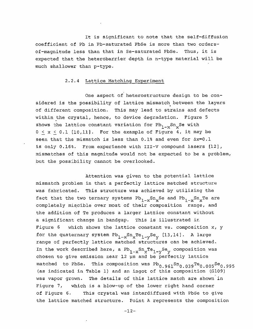
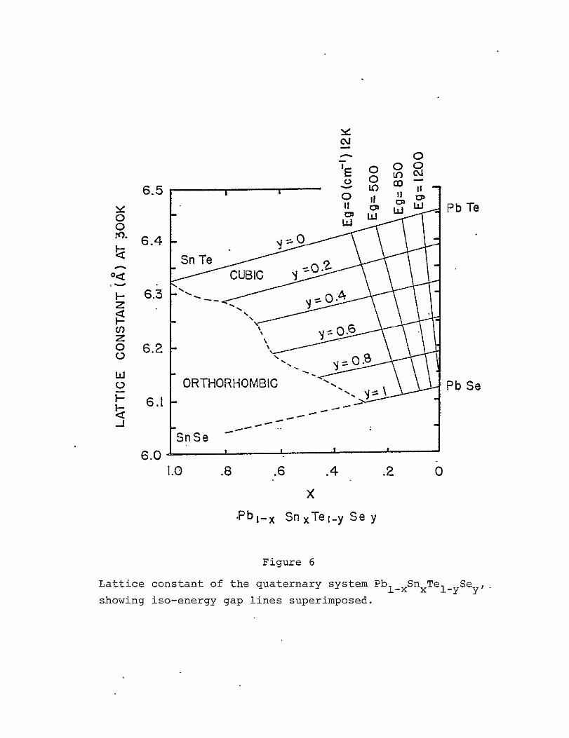
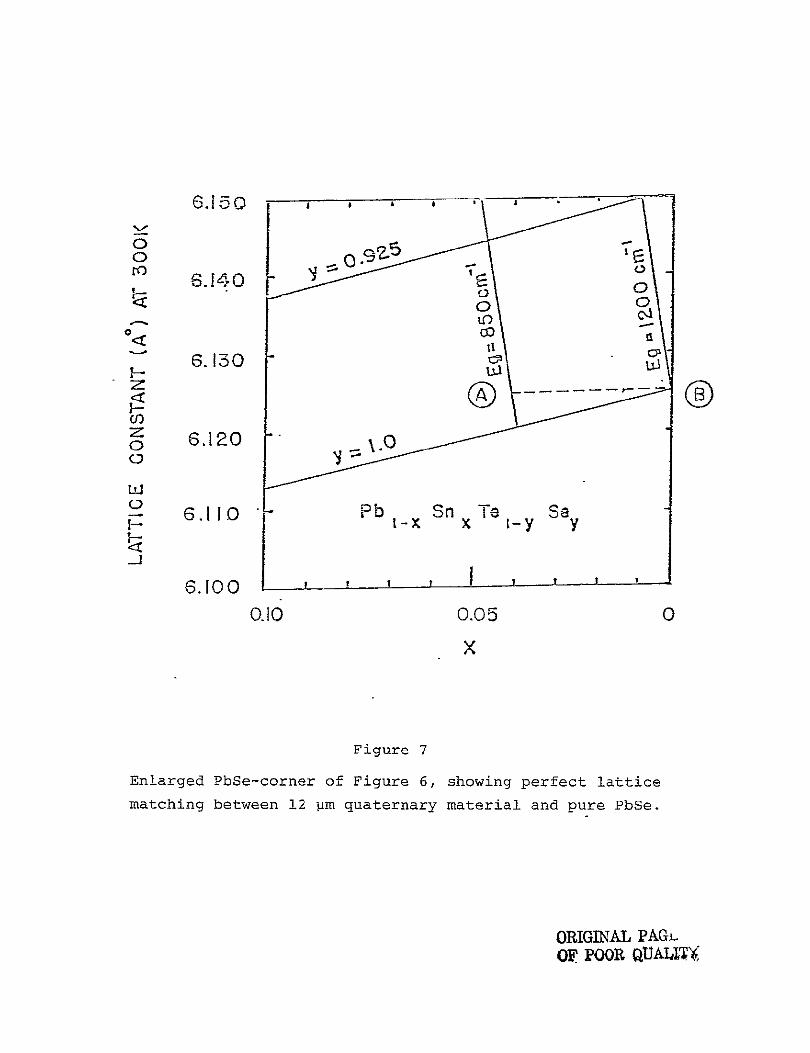