laser+photonics made in germany, austria & switzerland
TRANSCRIPT
�������� � ��������
74 Laser direct structuringCost-efficient 3D interconnect devices via LDS
28 Guide star lasers20 W tuned and stable at sodium’s D2 line
4 High-end photographic lenses The mastery of photographic optics
4 28 42 74
M A D E I N G E R M A N Y + A U S T R I A + S W I T Z E R L A N D
42 Ultra-sensitive CMOS sensorsPushing the low signal envelope of image detection
LA
SER
+PH
OTO
NIC
S 2
011
2011
01_Titel_LPX2011 15.12.2010 19:03 Uhr Seite 1
High-brightness laser diodes
While the achievable absolute peak out-puts previously characterized the re-quirements for a high-power laser diode,the usable optical power (the achievableintensity) is of prime interest today. Anew generation of laser diodes allowsfive to ten times higher intensities.
32
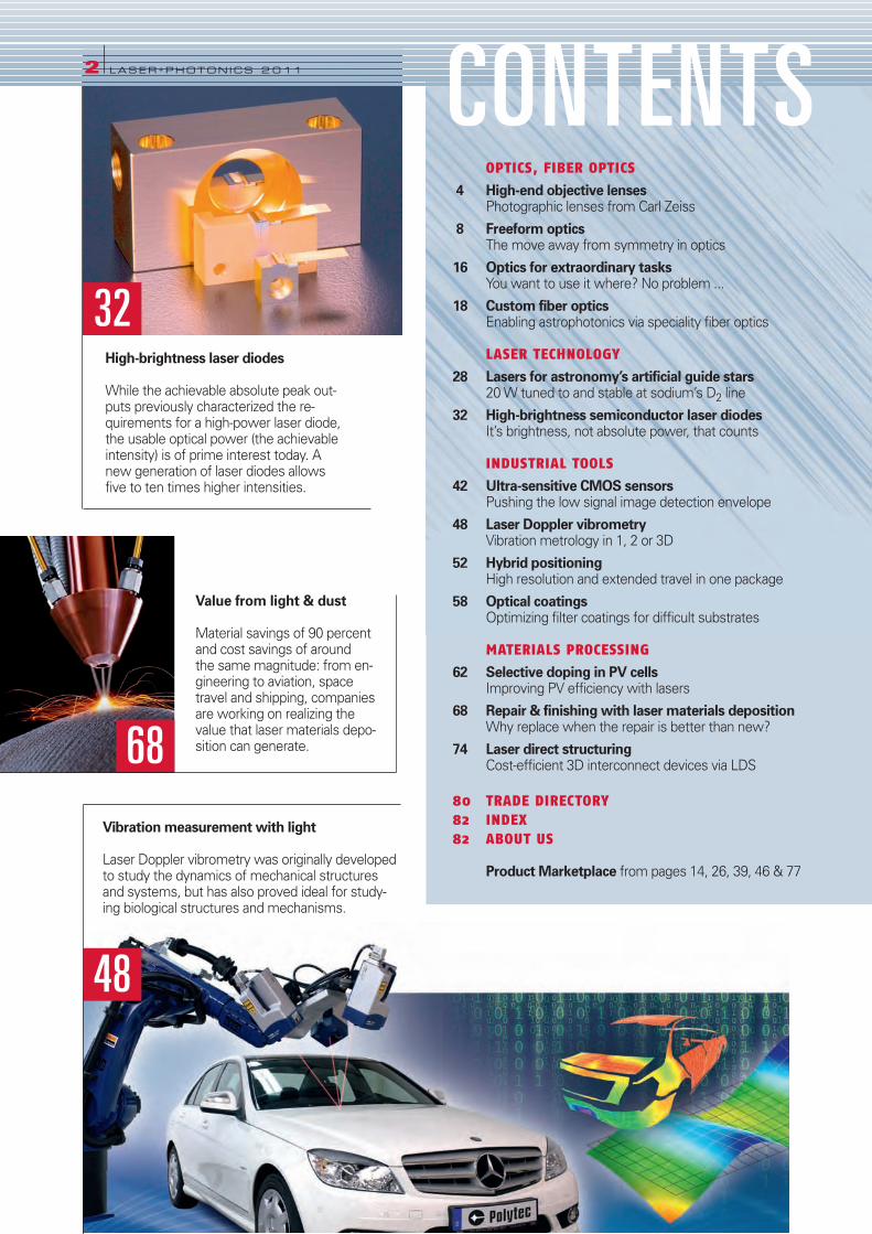
2 l LASER+PHOTONICS 2 0 11 CONTENTSOPTICS, FIBER OPTICS
4 High-end objective lenses Photographic lenses from Carl Zeiss
8 Freeform optics The move away from symmetry in optics
16 Optics for extraordinary tasks You want to use it where? No problem ...
18 Custom fiber optics Enabling astrophotonics via speciality fiber optics
LASER TECHNOLOGY
28 Lasers for astronomy’s artificial guide stars 20 W tuned to and stable at sodium’s D2 line
32 High-brightness semiconductor laser diodes It’s brightness, not absolute power, that counts
INDUSTRIAL TOOLS
42 Ultra-sensitive CMOS sensors Pushing the low signal image detection envelope
48 Laser Doppler vibrometry Vibration metrology in 1, 2 or 3D
52 Hybrid positioning High resolution and extended travel in one package
58 Optical coatings Optimizing filter coatings for difficult substrates
MATERIALS PROCESSING
62 Selective doping in PV cells Improving PV efficiency with lasers
68 Repair & finishing with laser materials deposition Why replace when the repair is better than new?
74 Laser direct structuring Cost-efficient 3D interconnect devices via LDS
80 TRADE DIRECTORY82 INDEX82 ABOUT US
Product Marketplace from pages 14, 26, 39, 46 & 77
Value from light & dust
Material savings of 90 percentand cost savings of around the same magnitude: from en-gineering to aviation, spacetravel and shipping, companiesare working on realizing thevalue that laser materials depo-sition can generate. 68
48
Vibration measurement with light
Laser Doppler vibrometry was originally developedto study the dynamics of mechanical structuresand systems, but has also proved ideal for study-ing biological structures and mechanisms.

EDITORIAL l LASER+PHOTONICS 2011 l3
Peripheralvision
Dr. Gregory Flinn, [email protected]
2010 comes to an end amid enthusiastic market reports out of more orless every corner of the photonics industry. Certainly for most sectors,the volume of orders and the expected turnover for 2010 are approach-ing or are even forecast to exceed previous record levels. Although wecan expect some degree of normalization, the vital signs are still good. As usual, in this issue of Laser+Photonics: Made in Germany, Austria &Switzerland, you will find a selection of the best 2010 Laser+Photonikarticles – but in English. Supplementary to these, and for the very firsttime, there are some brand new contributions. All contributions origi-nate from companies and institutions based within the German-speak-ing regions Europe. The raison d’être of the magazine is to provide thoseoutside with a glimpse of the industry within. The themes represented here – optics development, laser technology,imaging technology, optical metrology and materials processing – cor-respond to the (admittedly, not only German-speaking) European pho-tonics industries’ major strengths. Missing from the list is perhaps onlyLED/OLED technology. Excluding perhaps materials processing and laser technology, Europedoes not necessarily dominate the entirety of any one of these indus-try sectors. The bulk of industrial optics are manufactured elsewhere,for example, as are industrial LEDs, but Europe does lie well up amongstthe leaders in terms of innovation. But is it necessary to command thefull width and breadth of a sector, from development through to manu-facture and onto integration and application, so that funding and pursuitof that sector still makes sense? What are, for example, the financialrepercussions for Europe in letting industrial component manufacturein any one sector drift away to foreign shores? To know this, one needs to understand the impact of photonics as akey enabler in greater industry. That is, what is the financial leverageexerted by photonics in the peripheral industries, industries wherephotonics makes a key contribution in manufacture and/or in the finalproduct. A new European Commission study, undertaken in 2010, hasattempted to shed some (initial) light on the significances here withinthe European context, with the results due for publication in 2011.
LASER SENSORSHIGH END
optoNCDT 2300Maximum Precisionwith 50kHz measuring rate
§ Measuring ranges from 2mm to 100mm
§ Adjustable measuring rate up to 50kHz
§ A-RTSC(Advanced-Real-Time-Surface-Compensation)For high stability and accuracy
§ Interface Ethernet / EtherCat
§ Compact, with integrated controller
MICRO-EPSILON94496 Ortenburg / GermanyTel. +49 85 42/[email protected]
www.micro-epsilon.com
NE W

JÜRGEN FAHLBUSCH
NORBERT D IETE
Astandard objective lens quickly exhibits its limits when
used beyond its design intention, which is why Carl
Zeiss provides tailored solutions for the types of
application that call for a specialized design. One prominent
example of a customized solution was the modification of a
Biogon 5.6/60 mm objective lens for Hasselblad (Figure 1).
This lens was included on the Apollo Moon mission in 1969
– the photographs taken included the world famous picture
of the very first footprint in the Sea of Tranquility.
The objective first had to be made suitable for use in the ex-
treme conditions in space and on the Moon. For example, the
optical design and the materials chosen needed to be adapted
for use in a vacuum as well as be tolerant of the extreme
temperature fluctuations. In addition, modifications were made
to the objective so that photographs could still be taken even
while handling the camera with space suit gloves.
Even the first aerial photographs of the large scale destruction
of New Orleans caused by Hurricane Katrina in 2005, which
moved people across the world so deeply, were also taken with
objectives especially developed by Carl Zeiss for this type of
application.
4 l LASER+PHOTONICS 2 0 11 lOPTICS
The right objective lens for every application CARL ZEISS DEVELOPS SPECIALIZED OPTICS even for the most de-
manding of technical applications. Carl Zeiss objective lenses are one of the most impor-
tant tools used by photographers and film makers and, additionally, play a crucial role
in many technical applications – from industry and production to measurement and
observation through to space travel. The breadth of applications for photographic objec-
tives is matched only by the differing requirements in terms of materials and function.
1 During the moon landing in 1969, the modifiedhigh-performance Biogon 5.6/60 mm objective lens from Carl Zeiss was used to takesome momentous photographs
04-07_LPX110065_LPX11 15.12.2010 17:26 Uhr Seite 4

Designed to do the job at hand
Admittedly, specialist optics cannot cover all applications, but
each and every objective is made to perform exceptionally well
in its intended application. Together with their customers, the
expert teams in Oberkochen and Jena develop highly special-
ized solutions for use in harsh production environments, for ex-
ample, with exposure to dust and under extreme temperature
conditions. »The first step is to produce a feasibility study for
the customer and a framework for the likely cost,« explains
Jürgen Fahlbusch, Product Manager for Industrial Lenses at
Carl Zeiss. Cost is a very important factor when considering
specialist objectives, as it can often increase almost exponen-
tially depending on the actual challenge presented to develop-
er and materials. »Some types of optical glass are more ex-
pensive than gold,« Fahlbusch continues, »so it is essential to
analyze exactly what the objective will be used for and to
determine the requisite properties needed by the glass.« De-
veloping a highly specialized objective lens for technical appli-
cations can sometimes take several years and often involves
close collaboration with the customer throughout.
Eagle-eyed
Customized lens solutions from Carl Zeiss are particularly in
demand in photogrammetry. »This is a very complex but ex-
tremely relevant area,« says Norbert Diete, Product Manager
for the corresponding aerial photography lenses at Carl Zeiss.
»We increasingly encounter aerial photographs in our daily lives
– a great example is Google Earth – but many people do not
realize how difficult it is to take these types of photographs.«
With photogrammetric measurement methods, aerial photo-
graphy (Figure 2) provides organizations with important infor-
mation on the earth’s surface, for example on its composition.
Areas of forestry land that are damaged and the effects of a
recent hurricane are just two examples. In addition, the exact
routing for roads and sewers can be determined to within a few
centimeters, and the photographs also provide assistance in
the planning of industrial and residential areas.
Measurements are carried out using contiguous and overlap-
ping pictures. By capturing the earth’s surface from different
perspectives, software can be used to calculate a three-
dimensional model. In the past, aerial photographs were taken
in 23x23 cm2 negative format, requiring correspondingly bulky
camera equipment. Nowadays, photogrammetry is digital. The
resolution of the objective lenses must be precisely matched
to the pixel size of the CCD sensors in order to prevent an
›aliasing effect‹ in the image data.
One of the leading suppliers of aerial cameras is Intergraph Z/I,
based in Aalen, Germany. Intergraph’s ›DMC‹ (Figure 3), ›RMK-
D‹ and ›DMC II‹ digital camera systems enable three-dimen-
sional data to be captured with optimum geometric and radio-
metric precision. This type of data is important for urban and
landscape planning, for remote observation of agriculture and
forestry, and also forms the basis for data included in geo-
information systems.
Carl Zeiss has developed various different objective lenses for
Intergraph, all designed to handle the specific requirements
associated with operation in aircraft at altitudes of anywhere
between several hundred and several thousand meters. Issues
include the extreme temperature fluctuations – even when it
is warm and summery on the surface of the earth, tempera-
tures at altitude can be as low as -40°C. The objective, which
was sitting on the runway in the aircraft just a few minutes
earlier, is relatively quickly subject to an ambient temperature
difference of 50°C or more, and this for several hours.
Conventional photographic objectives would exhibit a sig-
nificant loss of performance, but for the calibrated and metric
Carl Zeiss aerial photography objectives, these temperature
OPTICS l LASER+PHOTONICS 2011 l5
2 Picture taken with a digital aerial camera (type RMK-D, altitude approximately 1000 m), and enlarged detail of a house
3 Digital camera system (DMC II) from Intergraph with optics from Carl Zeiss V
04-07_LPX110065_LPX11 16.12.2010 18:23 Uhr Seite 5
fluctuations are the norm. They can also withstand severe
pressure fluctuations and huge mechanical loads due to vibra-
tions or turbulence. In order to minimize these issues, the
experts at Carl Zeiss simulate in advance how the materials
will behave at different temperatures and vibrations and adapt
the optical design and the construction accordingly.
Besides the highly qualified and experienced development
team, Carl Zeiss is also equipped with the proper measurement
capability necessary for developing and manufacturing exactly
this type of sophisticated optical system. Each objective lens
is especially developed and is in many cases unique and un-
surpassed in terms of accuracy and performance.
Minimally but decidedly different
Next to the large-scale images taken to measure the earth's
surface, the detail examined in some production processes is
minute in comparison. For example, the complexity of form
presented by modern aluminum profiles quickly illustrates the
limits of the human eye. At the same time, the allowable
tolerance in production is very small – just a fraction of a milli-
meter can mean that a profile must be rejected, as a window
frame thus produced would not hermetically seal. Production
of such profiles is complex and susceptible to errors. A mini-
mal drop in temperature, a slight increase in pressure or a tool
that is just a little too worn can all result in profile dimensions
that fall outside the allowable tolerance. This makes reliable
quality assurance absolutely essential for manufacturing.
In the past, manufacturers had to send a sample section of the
profile to the lab at the end of a production run. If a fault was
identified, the entire batch had to be reprocessed. The com-
pany Ascona from Meckenbeuren, Germany, a leading manu-
facturer of solutions for optical profile measurement, has
developed an imaging system that enables quality control to be
carried out during production
itself. The secret lies in the
innovative construction of the
device. The profile section is
positioned horizontally and,
rather than being profiled
mechanically, it is photo-
graphed from the front. This
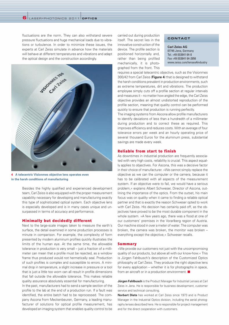
requires a special telecentric objective, such as the Visionmes
300/42 from Carl Zeiss (Figure 4) that is designed to withstand
the harsh conditions prevalent in production environments, such
as extreme temperatures, dirt and vibrations. The production
employee simply cuts off a profile section at regular intervals
and measures it – no matter how angled the edge, the Carl Zeiss
objective provides an almost undistorted reproduction of the
profile section, meaning that quality control can be performed
quickly to ensure that production is running perfectly.
The imaging systems from Ascona allow profile manufacturers
to identify deviations of less than a hundredth of a millimeter
during production and to correct these as required. This
improves efficiency and reduces costs. With an average of four
tolerance errors per week and an hourly operating price of
several thousand Euros for the aluminum press, substantial
savings are made every week.
Reliable from start to finish
As downtimes in industrial production are frequently associa-
ted with very high costs, reliability is crucial. This aspect equal-
ly applies to objectives. For Ascona, this was a decisive factor
in their choice of manufacturer. »We cannot simply replace the
objective as we can the computer or the camera, because it
has to be calibrated with all aspects of the measurement
system. If an objective were to fail, we would have a serious
problem,« explains Albert Schweser, Director of Ascona, out-
lining the importance of the optics. From the outset, his main
focus was on quality when it came to finding a reliable optical
partner and that is exactly the reason Schweser opted to work
with Carl Zeiss. His decision has certainly paid off, as the ob-
jectives have proved to be the most durable component in the
whole system. »A few years ago, there was a flood at one of
our customers’ premises in the Vorarlberg region of Austria.
Our machine stood in over a meter of water. The computer was
broken, the camera was broken, the monitor was broken –
everything except the objective,« Schweser recalls.
Summary
»We provide our customers not just with the uncompromising
quality of our products, but above all with our know-how.« This
is Jürgen Fahlbusch’s description of the Customized Optics
philosophy at Carl Zeiss. They produce the right objective lens
for every application – whether it is for photographs in space,
from an aircraft or in a production environment. ■
Jürgen Fahlbusch is the Product Manager for Industrial Lenses at Carl
Zeiss in Jena. He is responsible for business development, customer
service and technical consulting.
Norbert Diete has worked at Carl Zeiss since 1973 and is Product
Manager in the Industrial Optics division, including the aerial photog-
raphy lenses described here. He is responsible for project management
and for the direct cooperation with customers.
6 l LASER+PHOTONICS 2 0 11 lOPTICS
4 A telecentric Visionmes objective lens operates even in the harsh conditions of manufacturing
Carl Zeiss AG 07745 Jena, Germany
Tel. +49 (0)3641 64-0
Fax +49 (0)3641 64-2856
www.zeiss.com/lenses4industry
CONTACT
04-07_LPX110065_LPX11 15.12.2010 17:26 Uhr Seite 6

Reach new heights … Discover the !
Qioptiq offers the most comprehensive set of technologies for almost any photonic applicationComponents, modules and systems with superior specifi cations:
Optimum optical resolution
Highest transmission
Superior beam quality
Decades of interdisciplinary experience in many markets enable us
to provide a portfolio of design, technologies and manufacturing capabilities
suitable for your specifi c application.
Discover the full photonic excellence of Qioptiq!
US/Can: 800-429-0257
Eur: +49 551 69 35-0
Asia: +65 64 99 77 66
www.qioptiq.com
IndustrialManufacturing
Defense &Aerospace
Research &Development
Medical &Life Sciences
04-07_LPX110065_LPX11 15.12.2010 17:26 Uhr Seite 7

RAMONA EBERHARDT
In the future, the development of new optical imaging and
lighting systems will require that all degrees of freedom
be used in system design to develop competitive lens
equipment. Indeed, the number of patent applications relating
to the use of freeform surfaces of enhanced quality (<10 µm)
has sharply increased in recent years due to the versatility of
these lenses.
One constraint imposed on their design by manufacturing tech-
nology relates to the feasibility of given surface geometries.
The state-of-the-art involves the use of optical components on
which the optically active surfaces exhibit aspherical deviation
of one degree of freedom; these are known as aspherical
optical elements. It should however be kept in mind that as-
pherical lenses still possess rotational symmetry.
Away from symmetry
Modern system design is a precursor to the utilization of all
degrees of freedom for the surfaces of lenses or mirrors, such
that there no longer be
any restrictions on the
optically refractive or re-
flective active surface.
By eliminating the re-
quirement of symmetry
in system design, inno-
vative lens designs will
be possible in the future
– designs that have until now been regarded as unrealistic.
Unique optical imaging features, such as the correction of
aberrations and compact beam guidance of laser beam sources
(Figure 1), will be possible. In many cases, the use of innova-
tive freeform optical components should enable the develop-
ment of completely new features for a given optical system.
First specific applications
Freeform optics offer the system designer many possibilities,
such as the reduction of the number of optical components in
a system through the high degree of freedom, thus resulting
in an extremely lightweight design. In addition, and for the first
time, it is now possible to adapt them to applications involving
asymmetric beam guidance, as indicated above.
Initial design concepts derive from glasses delivering virtual
or augmented reality data, generally termed head-mounted de-
vices (HMDs), where beam guidance resulting from the geom-
etry of the head is directed in-line with the latter using freeform
optical elements.
The automotive industry represents another market. Important
traffic, speed and routing information, as well as warning
8 l LASER+PHOTONICS 2 0 11 lOPTICS
Freeform optics THE CHALLENGE FOR FUTUREOPTICAL SYSTEMS. In ophthalmology, technologies for
manufacturing freeform surfaces with sur-
face tolerances < 20 µm are already in use
in serial production. From requiring two
sets of eyeglasses for correcting near and
far sightedness, eyeglass ophthalmics is
now at the point where it can deliver pro-
gressive varifocal lenses custom-designed
to the needs of the wearer.
Fraunhofer Institute for AppliedOptics & Precision Engineering (IOF)07745 Jena, Germany
Tel. +49 (0)3641 807-0
www.iof.fraunhofer.de
CONTACT
1 Freeform surface for beam formation of a laser source,illustrated with the tool cutting path
© LASER+PHOTONICS
Freeform geometry and tool path
08-09_LPX110066_LPX11 15.12.2010 17:29 Uhr Seite 8
messages, can now be projected onto the windscreen, within
the visual field of the driver. These so-called head-up displays
(HUDs) are based on large-surface freeform mirrors that are
manufactured to exacting standards of geometric precision and
surface finish in a replication process suitable for mass pro-
duction.
Manufacturing processes
The degree of accuracy, materials, the quantity required and
the associated costs all determine which of several processes
can be used to manufacture freeform components. At the
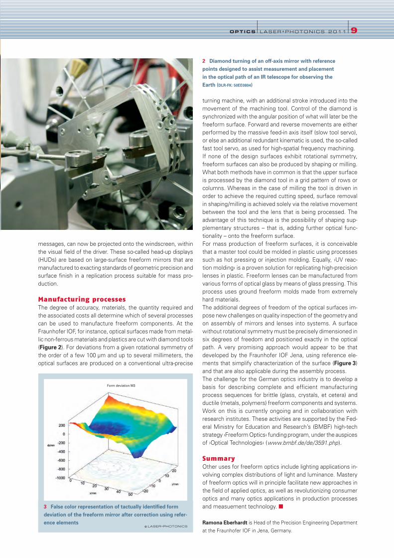
Fraunhofer IOF, for instance, optical surfaces made from metal-
lic non-ferrous materials and plastics are cut with diamond tools
(Figure 2). For deviations from a given rotational symmetry of
the order of a few 100 µm and up to several millimeters, the
optical surfaces are produced on a conventional ultra-precise
turning machine, with an additional stroke introduced into the
movement of the machining tool. Control of the diamond is
synchronized with the angular position of what will later be the
freeform surface. Forward and reverse movements are either
performed by the massive feed-in axis itself (slow tool servo),
or else an additional redundant kinematic is used, the so-called
fast tool servo, as used for high-spatial frequency machining.
If none of the design surfaces exhibit rotational symmetry,
freeform surfaces can also be produced by shaping or milling.
What both methods have in common is that the upper surface
is processed by the diamond tool in a grid pattern of rows or
columns. Whereas in the case of milling the tool is driven in
order to achieve the required cutting speed, surface removal
in shaping/milling is achieved solely via the relative movement
between the tool and the lens that is being processed. The
advantage of this technique is the possibility of shaping sup-
plementary structures – that is, adding further optical func-
tionality – onto the freeform surface.
For mass production of freeform surfaces, it is conceivable
that a master tool could be molded in plastic using processes
such as hot pressing or injection molding. Equally, ›UV reac-
tion molding‹ is a proven solution for replicating high-precision
lenses in plastic. Freeform lenses can be manufactured from
various forms of optical glass by means of glass pressing. This
process uses ground freeform molds made from extremely
hard materials.
The additional degrees of freedom of the optical surfaces im-
pose new challenges on quality inspection of the geometry and
on assembly of mirrors and lenses into systems. A surface
without rotational symmetry must be precisely dimensioned in
six degrees of freedom and positioned exactly in the optical
path. A very promising approach would appear to be that
developed by the Fraunhofer IOF Jena, using reference ele-
ments that simplify characterization of the surface (Figure 3)
and that are also applicable during the assembly process.
The challenge for the German optics industry is to develop a
basis for describing complete and efficient manufacturing
process sequences for brittle (glass, crystals, et cetera) and
ductile (metals, polymers) freeform components and systems.
Work on this is currently ongoing and in collaboration with
research institutes. These activities are supported by the Fed-
eral Ministry for Education and Research’s (BMBF) high-tech
strategy ›Freeform Optics‹ funding program, under the auspices
of ›Optical Technologies‹ (www.bmbf.de/de/3591.php).
Summary
Other uses for freeform optics include lighting applications in-
volving complex distributions of light and luminance. Mastery
of freeform optics will in principle facilitate new approaches in
the field of applied optics, as well as revolutionizing consumer
optics and many optics applications in production processes
and measuement technology. ■
Ramona Eberhardt is Head of the Precision Engineering Department
at the Fraunhofer IOF in Jena, Germany.
OPTICS l LASER+PHOTONICS 2011 l9
3 False color representation of tactually identified formdeviation of the freeform mirror after correction using refer-ence elements
© LASER+PHOTONICS
2 Diamond turning of an off-axis mirror with referencepoints designed to assist measurement and placementin the optical path of an IR telescope for observing theEarth (DLR-FK: 50EE0804)
Form deviation M3
08-09_LPX110066_LPX11 15.12.2010 17:30 Uhr Seite 9

FISBA OPTIK AGOptical Solutions
Rorschacherstrasse 268
9016 St. Gallen
Switzerland
Phone: 0041 (0)71 282 31 31
Fax: 0041 (0)71 282 31 30
www.fisba.com
FISBA OPTIK AGFISBA OPTIK is a world leader in optical sys-
tems, instruments and components. At FISBA
we develop and produce high-grade solutions
in the field of micro- and macro-optics. From
simple lenses to complex optical components
and systems, the optical solutions created by
FISBA are perfectly tailored to the specific cus-
tomer needs.
All aspects of optical expertise underone roof
FISBA unites all required disciplines and expert
knowledge under one roof. Lens designers and
engineers, backed by specialists in physics and
coating technology, develop, analyze and opti-
mize optical systems and components for the
entire spec¬tral range from UV to NIR — in-
tegrated and sustainable.
New technologies for affordableglass optics
FISBA employs and develops leading tech-
nologies to provide outstanding results for
every production stage, from prototypes to-
complex optics in large-scale production. Un-
compromising quality control vouches for flaw-
less products that render incoming goods in-
spection superfluous, saving valuable time and
in¬creasing process stability.
Newest technologies are implemented not on-
ly to offer customers the best optic solutions
for their application but at a reasonable price
as well. FISBA employs precision glass mold-
ing for the production of glass optics with ar-
bitrary forms in larger lots at a fair price, open-
ing up totally new possibilities in the cus-
tomer’s system development and assembly
optimization.
Product Portfolio
Advanced Optical Components
• Precision molded lenses
• Fast axis collimation lenses (FACs)
• FISBA Beam Twister™
• Aspheres
Optical Systems
• Lens systems
• Objectives
• Laser Modules
• Laser Optics
• Collimators
• Illumination
Optical Microsystems
Application Fields
• Biophotonics
• Bildverarbeitung und Sensorik
• Industrielle Fertigung
• Sicherheit und Verteidigung
• Weltraum und Astonomie
10 lCOMPANY PROF ILE
FirmenPortr_LPex2011 16.12.2010 18:25 Uhr Seite 10
COMPANY PROF ILE l11
COMPANY PROF ILE
LAYERTEC, established in 1990 as a spin off
from the Friedrich-Schiller-Universität Jena,
produces high quality optical components for
laser applications in the wavelength range from
the VUV (157nm) to the NIR (~4µm).
The company combines a precision optics
facility and a variety of coating techniques
(magnetron sputtering, thermal and e-beam
evaporation).
The precision optics facility of LAYERTEC
produces plane and spherically curved mirror
substrates, lenses and prisms of fused silica,
optical glasses like BK7 and some crystalline
materials, e. g. calcium fluoride. Fused silica
and calcium fluoride can be offered with rms-
roughnesses as low as 0.15nm.
Components for the UV are coated by evapo-
ration techniques. Coatings for the VIS and NIR
are mostly produced by magnetron sputtering.
This special coating process yields amorphous
layers with a very high packing density result-
ing in lowest straylight losses and a high ther-
mal and climatical stability of the optical pa-
rameters. Furthermore, the coatings are opti-
mized for high laser damage thresholds.
LAYERTEC has developed magnetron sput-
tering for optical coatings from a laboratory
technique to a very efficient industrial process.
The main products of LAYERTEC are· High – power - coatings for the NIR (e.g. for
Nd:YAG-, Ho:YAG- and Er:YAG-lasers)
· Femtosecond laser mirrors with exactly
determined phase properties (low GDD or
negative GDD and R>99.9%)
· Steep edge filters, e.g. HR 1030nm >99.9%
+ R(980nm)<1% with high laser damage
thresholds
· Low loss laser mirrors (R>99.99 in the VIS
and NIR)
· Coatings on laser- and nonlinear optical crys-
tals
· Metallic mirrors and coatings (Au, Ag, Al, Cr)
· Coatings for all excimer laser wavelengths
including 157nm
Besides the development of efficient coating
plants LAYERTEC has preserved its capabili-
ties for flexible production and the develop-
ment of prototypes and OEM components.
LAYERTEC – optische Beschichtungen GmbH
Ernst-Abbe-Weg 1
99441 Mellingen
Germany
Phone +49 (0)36453 744-0
Fax +49 (0)36453 744-40
www.layertec.de
Polytec GmbHPolytec-Platz 1–7
76337 Waldbronn
Germany
Phone +49 (0)7243 604-0
Fax +49 (0)7243 69944
www.polytec.com
Polytec GmbH For over 40 years Polytec develops and man-
ufactures high-quality measurement systems
for the analysis of vibration, length, speed and
surface topography. The applications range
from microsystem technology to large scale
mechanical engineering for the automotive
sector and aerospace industry, medical tech-
nology,biomedical sciences, etc. These Poly-
tec products are well known around the world
as the gold standard in non-contact, laser-
based measurement of vibration,speed and
length. Advanced product development re-
mains a core strategic activity at Polytec with
new electro-optical systems designed for an-
alytical process measurement, NVH analysis
and factory automation.
Besides laser technology, Polytec manufac-
tures optical spectrometer systems and com-
ponents for various applications in process an-
alytics covering the whole range from OEM
products to turn key solutions.
The third focus of the Polytec business is the
distribution and service for opto-electronic
components and modules as well as complete
measurement systems for various applica-
tions. Polytec focuses on machine vision,
lasers and laser systems, fiber optic sensing,
optical telecommunication, optical radiation
measurement, spectroscopy, semiconductor
and photovoltaics, metrology as well as on
electro-optical test systems.
Polytec has staffed offices throughout Europe,
North America and Asia to provide customers
with the best local sales, service and support
in the industry.
FirmenPortr_LPex2011 15.12.2010 12:21 Uhr Seite 11

NanoFocus AGLindnerstr. 98
46149 Oberhausen
Phone +49 (0) 208-62000-0
Fax +49 (0) 208-62000-89
www.nanofocus.de
Fast and precise 3D Surface
Metrology Solutions for
Laboratory and Production
NanoFocus develops, manufactures and dis-
tributes high-resolution optical 3D metrology
systems and corresponding software solutions
for laboratory and production environments.
The flexible systems permit fast, simple, and
non-contact measurements of 3D topography
with resolution in the nanometer range. These
reliable instruments are designed for surface
roughness analysis according to DIN EN ISO,
structure- or micro- geometry, as well as layer
thickness measurements of technical sur-
faces.
The components used for the NanoFocus
metrology systems go through strict selection
and validation processes to guarantee highest
quality standards, stability and low-mainte-
nance. The product range comprises 3 differ-
ent lines: the µsurf confocal microscopes, the
µscan laser profilometers, and the µsprint
high-speed inline metrology systems. The
powerful µsoft software tools provide a vari-
ety of analysis options as well as automated
measurement and evaluation processes.
Analysis can be performed using the ISO
4287/4288 traditional 2D parameters as well
as new 3D parameters, in accordance with
ISO 25178. The combination of robust hard-
ware and versatile software provide users with
a universal tool to reliably quantify engineered
surfaces. With the automation software,
measurements can be processed at a high
throughput rate with highest efficiency and
without user influence.
The NanoFocus technologies offer various ad-
vantages for the characterization of technical
surfaces in the micro and nanometer ranges,
Contrary to a SEM (x,y) for example, NanoFo-
cus´ confocal technology offers the data in true
3-dimensional coordinates (x,y,z). Only with
this quantitative data an exact analysis of 3D
surface parameters can be performed, deliv-
ering a larger range of information about the
surface texture. Additionally, this technology
does not require preparation of the measure-
ment sample. Already
after a few seconds,
meaningful data is pro-
vided for further ana-
lysis.
More than 700 Nano-
Focus metrology sys-
tems are in operation
worldwide. NanoFo-
cus customers include
well-known compa-
nies from all major in-
dustries, such as auto-
motive, photovoltaic
and electronics indus-
tries, the medical sec-
tor, forensics and me-
chanical engineering,
as well as renowned
universities and re-
search institutes.
12 lCOMPANY PROF ILE
FirmenPortr_LPex2011 15.12.2010 12:21 Uhr Seite 12

COMPANY PROF ILE l13
BERLINER GLAS GROUP - Your Partner forOptical SolutionsAs one of the leading European OEM suppli-
ers of optical components and systems,
BERLINER GLAS GROUP offers technically ad-
vanced optical solutions supporting manufac-
turers of devices that utilize the broad spec-
trum of light. Our focus markets are space,
geosystems, metrology, laser, medical, de-
fense and semiconductor technologies. With
a high flexibility in regards to these technolo-
gies, our solutions are always developed in
close cooperation with our customers and re-
sult in serial production using leading edge ma-
terial and manufacturing technology.
The BERLINER GLAS GROUP consists of com-
panies which have been developing and pro-
ducing optical solutions for over 100 years. With
around 950 employees, we provide tailor-made,
market driven solutions of the highest quality.
Engineering
• System engineering • Optical and mechani-
cal design • Coating design • Customer-spe-
cific metrology
Key-Components
• Spherical lenses • Aspherical lenses • Cylin-
drical lenses • Plano optics • Prism systems
• Microstructuring • Coatings • coating design
• Filter • Mirror • Beam splitter/combiner • ITO
coating • Holographic gratings
Assemblies Systems
• Optical, optomechanical and electro optical
systems • Lens systems • Objectives, zoom
systems • Measuring systems • Cameras •
Laser systems • Light sources • Lighting sys-
tems
Berliner Glas KGaAHerbert Kubatz GmbH & Co.Waldkraiburger Str. 5
12347 Berlin, Germany
Phone +49 (0)30 60905-0
SwissOptic AGHeinrich-Wild-Strasse
9435 Heerbrugg, Switzerland
Phone: +41 (0)71 727-3074
www.berlinerglasgroup.com
COMPANY PROF ILE
SIOS Meßtechnik GmbHAm Vogelherd 46
D-98693 Ilmenau/Germany
Phone 03677-64470
Fax 03677-64478
Email: [email protected]
www.sios.deUSA Piezosystem Jena Inc., Mr Litynski
www.piezojena.com
P. R. of ChinaTianjin MicroNano Manufacturing Tech Co.,
Ltd.; Dr. Chen, www.mn-mt.com
UK Armstrong Optical Ltd., Mr Routledge
www.armstrongoptical.co.uk
France Trioptics France, Mr Lioutier
www.trioptics.fr
Miniature plane-mirrordifferential interferometer
The SP-DIS series miniature
plane-mirror differential inter-
ferometers are high-precision
length measurement instru-
ments. They are especially
suitable for the measurement
and calibration of mirror sur-
faces, for parallelism meas-
urements and for measure-
ments against a fixed refer-
ence.
The interferometers are easily adapted to suit
a wide variety of experimental setups and
tasks. The miniaturized sensor head allows for
their use as permanently mounted measure-
ment systems.
Planar mirrors or other optical-quality reflective
surfaces may be employed as reflectors. The
measuring arms are insensitive to misalign-
ment by as much as several minutes of arc
with respect to the laser beam without ad-
versely affecting the operation of the interfer-
ometer making it easy to set up and use. The
beam from the laser light source is transmit-
ted to the sensor head by a fiberoptic cable.
The miniature interferometer converts dis-
tance changes of the parallel mirrors along the
beam axis into optical interference signals that
are transmitted to an optoelectronic signal pro-
cessing/power supply unit for processing and
output.
Instrument operation and display of measure-
ment results are controlled either through a
separate keypad/display unit or an USB con-
nected PC running optional software.
FirmenPortr_LPex2011 17.12.2010 10:09 Uhr Seite 13
Reduces light scatterBlack chromium coating. Optics Balz-
ers has made use of the black chromium
properties, to date applied predominant-
ly in solar collectors and sunglasses, to
develop a coating for use in medical
devices and other applications. The ›Cr-
Black‹ black chromium coating is an opti-
cally black coating distinguished by its
high absorption capacity and its mini-
mized reflection in the VIS range. Its color
hue can be tailored to customers’ specific
requirements, for example to produce a
black chromium part with a blue compo-
nent. The coating’s high environmental
stability and durability, high adhesion on
glass and metal in conjunction with its
high application temperature of up to
250°C make it suitable for a wide variety
of uses. Thanks to the high reduction of
scattered light and its ROHS-conformity,
the CrBlack coating is ideally suited for
applications in lens systems of medical
devices. The ›CoatingPlus‹ capabilities of
Optics Balzers also enable CrBlack to be
patterned for demanding applications.
The whole-surface or patterned coating
can be easily cleaned following addition-
al process steps.
www.opticsbalzers.com
Precision molded Optics. Docter Optics has recently in-
troduced an industrially precision mold-
ed asphere with contour tolerances al-
lowing applications in imaging systems
and which, says the manufacturer, have
already proven themselves in practice.
Optical components produced in the
conventional way (ground and polished),
can therefore be replaced with precision
molded components in certain applica-
tions, considerably reducing the OEM
cost of medium class optics and high
volume products. Using the precision-
fast-molding process, Docter Optics
produces freeform lenses, light pipes, as-
pheres and arrays with a precision down
to 3 µm PV, contingent on geometry. De-
pending on the field of application, such
pressed optical components enable more
compact optical systems. In addition, this
technology allows the bearing surface or
alignment marks to be pressed in, as a
single component. In its Optical Systems
business section, Docter Optics also de-
velops and manufactures complete opti-
cal and optomechanical assemblies for
OEMs, thereby offering the full range of
services in the value-added chain.
www.docteroptics.com
Autoclave tolerantZoom lenses. Berliner Glas Medical
Applications is presenting individually
customized, developed and manufac-
tured zoom objectives for high resolution,
autoclave-tolerant endoscope cameras.
The zoom lenses generally comprise two
or three simple lenses, one of which can
be moved axially to change the focal
length, thereby magnifying the objects in
the field of vision. The zoom lenses are
characterized by a high resolution, impact-
resistance, low weight, compactness and
autoclave tolerance. They are designed
for at least 500 autoclaving cycles. Sys-
tems with full HD (1080x1920 pixels) can
be provided. Stepped or continuous shift-
ing between the desired focal lengths
may be either manually or motorized. The
dimensions of the zoom lens may be de-
signed either for applications ›in-the-tip‹
or for conventional zoom lenses at the
proximal end of the endoscope.
www.berlinerglas.de
14 l LASER+PHOTONICS 2 0 11 lPRODUCT MARKETPLACE
Patterned and pre-cut CrBlack coating
14-15_LPX_Produkte_LPX11 15.12.2010 17:32 Uhr Seite 14

For RGB/LED light mixing Optics. B&M Optik now offers glass
optics that promise excellent efficiency
and dynamic light color changes, allow-
ing the homogeneous mixing of large-
area RGB configurations, just as with
standard 4-chip LEDs. The dimensions of
the optics are determined by the size of
the LED radiating surface. Depending on
the choice of optics and additional fo-
cusing, it is possible to adjust the angle
of radiation as required and achieve
angles of up to 15°.
www.bm-optik.de
Especially suited for photovoltaics Lens systems. Sill Optics provides full
quartz lenses and telescopes with low-
absorption, high performance coatings
especially for use in laser systems for the
solar cell industry. They include the f-
theta lenses with a focal length of
330 mm and that are available in versions
for 355, 532 and 1064 nm. Sill supplies
appropriate telescopes for laser beam
diameter adjustment. Various expansion
factors of 1.0 to 20x are available for 355,
532 and 1064 nm. Any standard laser can
be adapted to the f-theta optics used.
www.silloptics.de
PRODUCT MARKETPLACE l LASER+PHOTONICS 2011 l15
45°
Application examples:Fiber collimator 60FC-Q-...Adjustment of integrated
QUARTER WAVE PLATE
Schäfter + Kirchhoff HamburgIntensity ProfileLaser Beam Analysis:
Ref.: SK970703 Intensities100.0%
90.0%80.0%70.0%60.0%50.0%40.0%30.0%20.0%10.0%
Object:
Fiber CollimatorCollimating Lens M12Beam Diameter (1/e2) 2.18 mmWavelength 635 nmLasersource Singlemode FiberMode Field Diameter 4 .5 μ mNumerical Aperture 0.11
Gaussian Fit
[email protected] www.SuKHamburg.de
Laser Beam Coupler for Singlemodefiber
inclined fiber coupling axis
Made i
n Germ
any
B
Made i
n Germ
any
A
Multiline
Laser Source
Components and Toolsfor Physics and (future)
Nobel Laureates
Postcard sized replace-ment for 1 m2 sized breadboard setup.
Laser Line-, Micro Focus- and Laser Pattern Generators
BeamProfile
Machine Vision Components
Components and Toolsfor Physics and (future)
Nobel Laureates
Made i
n Germ
any
bad
goodRetro Reflector
1
2
3
1. Power monitoring2. Beam combiner3. Retro reflector4. Tilt adjustment
color monochrome1.0
0.0400 600 800 1000
Spectralrange
Spectralrange
512 to 12000 pixels, monochrome and color
CCD Line Scan CamerasSK 9170: Gray Scale Line Signal – 0
SK 9170: Gray Scale Line Signal – 1
255
255
00
00
ZOOM
ZOOM
MicrosoftWindows xpProfessional
®
®
Made i
n Germ
any
with polarization-main-taining fiber optics
Laser Sources
MOT
agneto
ptical
raps
Special Fiber Collimators for Quantum Optics and for MOT
4 Tilt adjustment
BeamCombiner
Power monitoring
Fiber Port Clusters for
A Laser Beam Coupler60SMS-1-4-…
Polarization Analyzer Series SK010PA-...
Multiple Wavelength Ranges 350 – 1600nm
Analog: RS422
Digital: LVDSCameraLinkUSB 2.0
TM
B Fiber cable PMC-... C Fiber collimator 60FC-...D Micro focus optic 5M-...
Fiber optics polarization maintaining, for laser beam sources 350-1700nm
RGBV
Apochromatic correctedfiber optics 400 - 660 nm
405 460 532 660
NewProducts
C
D
PM fiber cables:Measurement of PER(Polarization extinctionratio) and polarization axis
AustriaFranceItalyChina
Republic of Korea
GermanyU.K.USAIndia
In global use:
All in one Characterization of assembled optics. Trioptics presents their new ›OptiCen-
tric 3D‹ as a solution for the complete
optomechanical characterization of as-
sembled optical systems, measuring
lens centering, air spacing, and center
thickness inside of assembled optical
systems with a single instrument. This
new approach integrates different lens
analysis technologies, combining the
›OptiCentric‹ centering error measure-
ment technology with a low coherence
interferometer called ›OptiSurf‹, which
measures the air gaps between lens
surfaces and the center thickness of
lenses within the optical system. The
cross-interaction of both measurement
systems enables a fast alignment of the
lens system, thus increasing overall
measurement accuracy. It provides de-
tailed manufacturing quality information,
being able to measure centering errors
of less than 0.1 µm as well as air spac-
ing and center thicknesses of less than 1 µm. The software has a two-level user
interface for complex analysis routines in the R&D phase and an intuitive and
user-friendly display for operators at the production site. www.trioptics.com
14-15_LPX_Produkte_LPX11 15.12.2010 17:32 Uhr Seite 15

GEORG ZE ITLHACK
THOMAS SCHÄFFLER
Ahistory of the Earth’s climate is stored in the ice of
the polar glaciers. Gases and aerosols trapped over
several hundred thousand years can be evaluated in
ice cores drilled from polar glaciers. The deepest ice core
drilling made to date in the Antarctic descends 3260 meters
and spans a period of more than
700000 years. These ice cores yield
detailed data about the environmen-
tal and climatic conditions that then
prevailed. The information gained is
of particular importance in the current
climate-related debates, and helps cli-
mate behavior to be inferred regard-
ing the role that modern industrial
society plays in global warming.
Tracing ice formation
The formation of ice on a glacier’s sur-
face is a complex process, influenced
by such factors as quantity of precipita-
tion, temperature, wind force and the
presence of trace elements. Glacial
snow is compacted by subsequent
layers of fresh snow on the glacial
surface into an air-permeable firn, and
with time this firn is gradually trans-
formed into layers of ice lying ever fur-
ther below the surface. As the upper
layers of the glacier are air permeable,
a temporal discrepancy can occur be-
tween the bubbles of trapped gases and
trapped aerosols that can extend any-
where from 100 to 10000 years.
Glaciologists of the Alfred Wegener
Institute analyze the microstructure of the ice cores to trace
the process of ice formation and glean information concerning
the development of the gas-containing air bubbles. The objec-
tive is to model these processes and reconstruct the past.
Fast image acquisition from ice samples
Samples of a manageable size are taken from the valuable ice
cores for image acquisition. The samples must be scanned as
quickly as possible otherwise subli-
mation changes the porous ice sur-
face, which in turn leads to distortion
of the information gained from the
images. To enable this rapid image
acquisition, Schäfter+Kirchhoff have
developed a scan macroscope that can
scan a large surface with high resolu-
tion. Figure 1 shows the macroscope
in use.
Schäfter+Kirchhoff specializes in de-
veloping image acquisition systems for
challenging applications, and often
implement line scan cameras they
develop themselves for this purpose.
Line scan cameras are most often
employed when the surface to be
analyzed is large and yet the smallest
details are essential. To obtain a two-
dimensional image, the object under
study is guided past the camera at a
16 l LASER+PHOTONICS 2 0 11 lOPTICS
Large area scanmacroscope
LOOKING BACK AT THE HISTORYOF THE EARTH’S CLIMATE. A large area
scan macroscope developed by Schäfter+Kirchhoff
enables scientists at the Alfred Wegener Institute for Polar
and Marine Research in Bremerhaven to analyze ice cores
rapidly and in great detail. This application stands out from conven-
tional inspection tasks, in particular because of the current relevance of global warming
issues. This innovative development uses Linos inspec.x L series lenses from Qioptiq.
Qioptiq Photonics GmbH & Co. KG 85622 Feldkirchen/Munich, Germany
Tel. +49 (0)89 255458-0
www.qioptiq.com
CONTACT
1 The scan macroscope system fromSchäfter+Kirchhoff in action
16-17_LPX110086_LPX11 15.12.2010 17:34 Uhr Seite 16
precisely defined speed and the image is assembled line by line.
The sensor in the Schäfter+Kirchhoff scan macroscope has
8192 pixels and achieves a resolution of 5 µm over a measuring
field width of 41 mm. Thanks to the high line rate of the sensor,
it takes just 2.8 seconds to measure a 41x100 mm2 area.
Stringent requirements for the optics
The need for such high resolution places enormous demands
on the optics. A feature size of 5 µm corresponds to a resolu-
tion of 100 lp/mm. With the required magnification of 1.4, this
is very close to the theoretical diffraction limit. Moreover, the
image data must fill out a sensor that is 57 mm long – compare
that to the image diagonal of a standard 35 mm camera, which
is just 43.3 mm. The lenses in the ›Linos inspec.x L‹ series from
Qioptiq were developed for just this type of application: ex-
tremely high resolution with long line sensors. In the scan
macroscope, the ›inspec.x L 5.6/105 0.76 x‹ is mounted back-
wards to give the required magnification of 1.4. Figure 2 shows
the results of scanning ice cores from various depths.
Extreme conditions
Not only the optical imaging quality, but the resilience of the
entire setup is also important for this application. After all, the
scanning of ice cores has to be carried out at a frosty 30°C
below freezing (Figure 3) in order to avoid changes that might
occur to the sample before and during image acquisition. At
Qioptiq, climate testing of lenses at temperatures down to
-25°C is standard procedure. That is why Qioptiq technicians
were confident that the lens would stand up well in the Antarc-
tic climate. Additional climate tests down to -40°C, as well as
simulations to evaluate the lens’s reaction to changes in tem-
perature, showed that the lens can withstand these extreme
conditions while maintaining its optical performance.
Summary
With the information gained regarding previous climate fluc-
tuations as well as improved knowledge of the relationships
between the principal indicators, scientists can better estimate
the likely behavior of the climate now subject to the pressures
of modern industrial society. As is so often the case, this type
of unique application requires equally performant components
in order to be able to realize the full potential – even in this
special case, standard Qioptiq optics components were able to
deliver the performance necessary. ■
Georg Zeitlhack is Vision Technology Sales Manager, and ThomasSchäffler is Head of the Vision Technology Market Segment at
Qioptiq Photonics, based in Feldkirchen, near Munich, Germany.
OPTICS l LASER+PHOTONICS 2011 l17
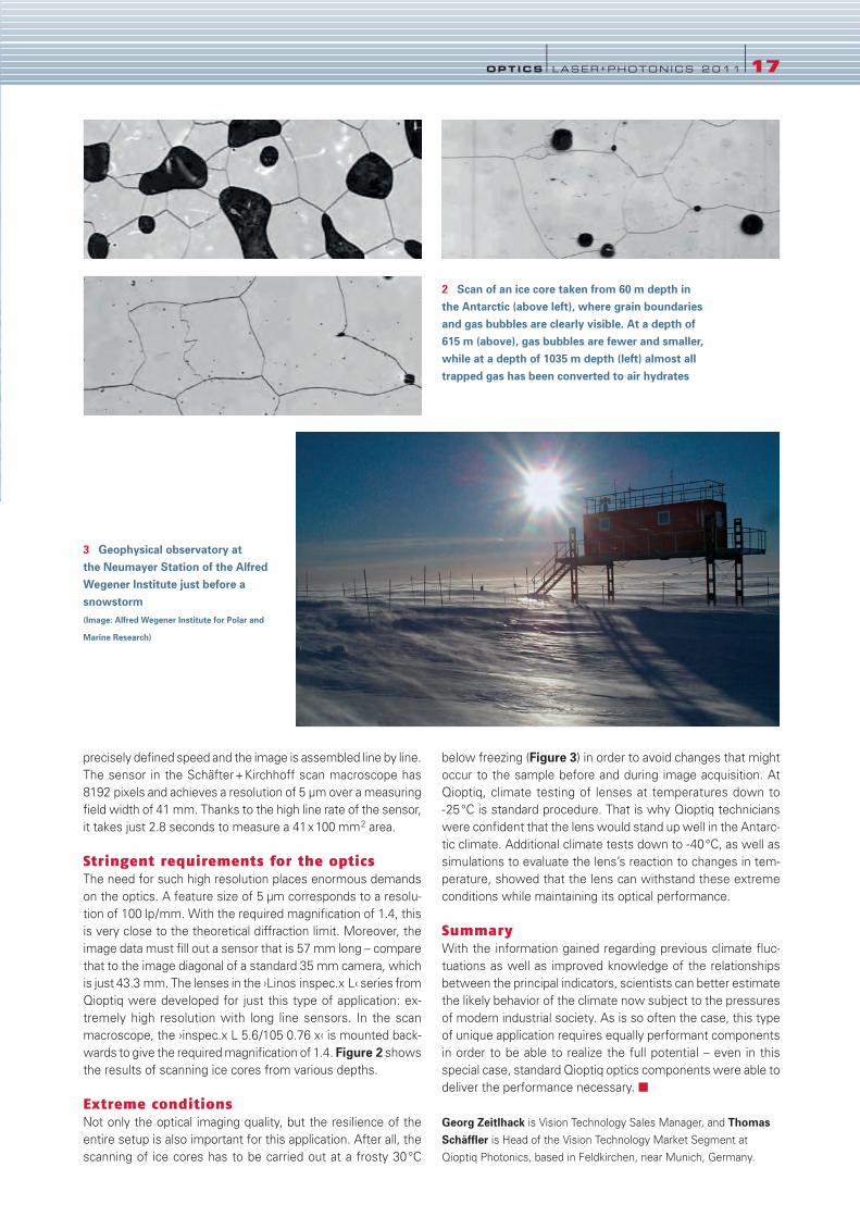
2 Scan of an ice core taken from 60 m depth inthe Antarctic (above left), where grain boundariesand gas bubbles are clearly visible. At a depth of615 m (above), gas bubbles are fewer and smaller,while at a depth of 1035 m depth (left) almost alltrapped gas has been converted to air hydrates
3 Geophysical observatory at the Neumayer Station of the AlfredWegener Institute just before asnowstorm (Image: Alfred Wegener Institute for Polar and
Marine Research)
16-17_LPX110086_LPX11 15.12.2010 17:34 Uhr Seite 17
MART IN M. ROTH
ANDREAS KELZ
LUZ MARINA CA IRÓS BARRETO
Appropriately for the International Year of Astronomy,
the 2009 Nobel Prize for Physics was awarded for
the development of optical glass fibers (Charles Kao)
and the CCD detector (Willard Boyle and George Smith), two
key technologies from the area of photonics that have been
used to make the most important discoveries in modern
observational astrophysics in the optical spectral range.
CCD imaging
The development of the CCD detector for scientific imaging on
satellite missions back in the 1980’s marked a genuine revolu-
tion in image sensors – and ultimately sounded the death knell
for celluloid.
The deepest view that mankind has ever had into the universe
is thanks to a total exposure of more than 100 hours with the
ACS camera on the Hubble Space Telescope (Figure 1). The
›Hubble Ultra Deep Field‹ (HUDF) shows more than 10000
galaxies, including the remotest objects that emitted their light
when the universe was just 10 percent of its current age since
the Big Bang – an image of incalculable value for cosmology
and extra-galactic astrophysics.
Scientists from all over the world can compare the brightness,
morphology, color and spatial distribution of galaxies with sim-
ulations on supercomputers, in order to understand the large
scale structure of matter in the universe and the evolution of
galaxies up to their current appearance. For example, in the
early stages of the universe, that is, among the weakest and
most distant objects, there is an above average abundance of
irregular dwarf galaxies – an indication that seems to confirm
18 l LASER+PHOTONICS 2 0 11 lF IBER OPTICS
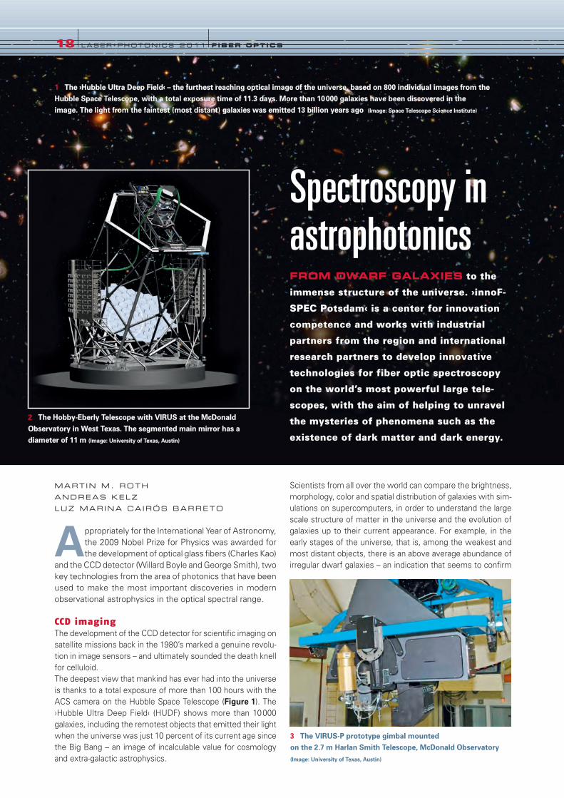
1 The ›Hubble Ultra Deep Field‹ – the furthest reaching optical image of the universe, based on 800 individual images from theHubble Space Telescope, with a total exposure time of 11.3 days. More than 10000 galaxies have been discovered in theimage. The light from the faintest (most distant) galaxies was emitted 13 billion years ago (Image: Space Telescope Science Institute)
Spectroscopy inastrophotonics FROM DWARF GALAXIES to the
immense structure of the universe. ›innoF-
SPEC Potsdam‹ is a center for innovation
competence and works with industrial
partners from the region and international
research partners to develop innovative
technologies for fiber optic spectroscopy
on the world’s most powerful large tele-
scopes, with the aim of helping to unravel
the mysteries of phenomena such as the
existence of dark matter and dark energy.
2 The Hobby-Eberly Telescope with VIRUS at the McDonaldObservatory in West Texas. The segmented main mirror has adiameter of 11 m (Image: University of Texas, Austin)
3 The VIRUS-P prototype gimbal mounted on the 2.7 m Harlan Smith Telescope, McDonald Observatory(Image: University of Texas, Austin)
18-21_LPX110056_LPX11 15.12.2010 17:37 Uhr Seite 18
the theory of a hierarchical scenario for the formation of
galaxies, which manifests itself as a continuous merging
process from dwarf galaxies to constantly growing spiral or
elliptical galaxies.
Fiber optic multi-channel spectroscopy
Alongside direct imaging, spectroscopy is the most important
technology for observational astronomy in the optical spectral
range. Astrophysicists can compare spectra with theoretical
model calculations to identify physical state variables such as
gravity and temperature in stellar atmospheres, electron
density and temperature in ionized gas nebulae (›H II‹ regions,
planetary nebulae, supernova remnants), or the abundance of
chemical elements and the age of stars. By utilizing the Doppler
effect, the radial velocity of stars, gas nebulae and galaxies, as
well as the rotation speed and mass of galaxies can be meas-
ured. In addition, one can obtain proof of supermassive black
holes at the center of galaxies, the existence and mass of
extra-solar planets, and many other important astrophysical
variables.
Compared to direct imaging, spectroscopy is definitively more
informative, but is also much more costly. Depending on the
spectral resolution, objects with a continuous spectral energy
distribution typically require exposure times 100 to 10000 times
longer than for a broad band image to obtain the same signal
to noise ratio. In view of the exposure times of many hours per
object, which are indispensable on a modern 8m-class tele-
scope for galaxies with high redshift, the limits of feasibility are
quickly reached when we consider the sample sizes required
to test cosmological theories. As the operating costs alone for
a large telescope are approximately 50000 Euro per night of
observation, spectroscopy on all 10000 galaxies in the HUDF
would be inaffordable.
A solution to this dilemma has been found with the develop-
ment of multiplex systems, in which the spectra of multiple
individual objects within the telescope’s field of view can be
recorded simultaneously with just a single exposure (multi-
channel spectroscopy). With
multiplex factors in the
range of 300 to 5000, fiber
optical multi-channel spec-
trographs in astrophysics are
by far the most powerful
systems in the world.
When it comes to these in-
struments, we differentiate
between two basic sampling methods: multi-object spectro-
graphs, which use a positioning robot to move fiber probes to
any number of objects distributed across the field of view (one
fiber per object), or integral field spectrographs, which use a
fiber bundle to sample a contiguous two-dimensional field of
view (imaging spectroscopy).
The HETDEX project and the
VIRUS instrument in Texas
The Multichannel Spectroscopy Group based at the Astro-
physics Institute Potsdam (AIP) and belonging to the innoF-
SPEC Potsdam Center for Innovation Competence (supported
by the BMBF – German Ministry of Education and Research),
is focused on researching new technologies for these two
F IBER OPTICS l LASER+PHOTONICS 2011 l19
P I E Z O N A N O P O S I T I O N I N G
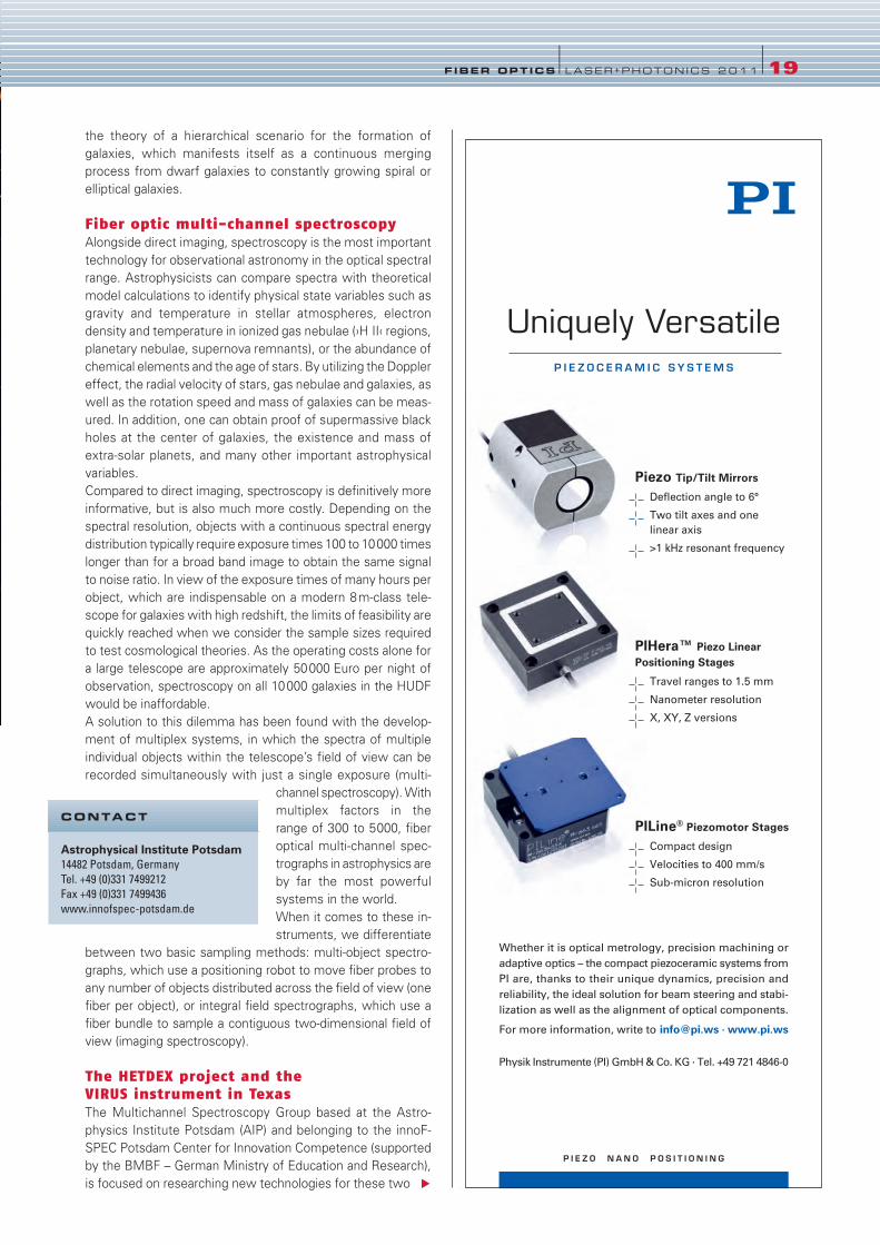
Piezo Tip/Tilt Mirrors
Deflection angle to 6°
Two tilt axes and one
linear axis
>1 kHz resonant frequency
Whether it is optical metrology, precision machining or
adaptive optics – the compact piezoceramic systems from
PI are, thanks to their unique dynamics, precision and
reliability, the ideal solution for beam steering and stabi-
lization as well as the alignment of optical components.
For more information, write to [email protected] · www.pi.ws
Physik Instrumente (PI) GmbH & Co. KG · Tel. +49 721 4846-0
Uniquely VersatileP I E Z O C E R A M I C S Y S T E M S
PIHera™ Piezo Linear Positioning Stages
Travel ranges to 1.5 mm
Nanometer resolution
X, XY, Z versions
PILine® Piezomotor Stages
Compact design
Velocities to 400 mm/s
Sub-micron resolution
pi_101111_kombi6_85x250_en.indd 1 01.12.10 15:28
Astrophysical Institute Potsdam14482 Potsdam, Germany
Tel. +49 (0)331 7499212
Fax +49 (0)331 7499436
www.innofspec-potsdam.de
CONTACT
V
18-21_LPX110056_LPX11 15.12.2010 17:37 Uhr Seite 19

key applications in astrophysics – preferentially those consid-
ered to additionally have significant potential for technology
transfer, in particular into medical technology, food sciences
and pharmaceuticals.
The most interesting current projects include the development
of the VIRUS (Visual Integral-field Replicable-Unit Spectrograph)
instrument (Figure 2), which, as part of the ›Hobby-Eberly Tele-
scope Dark Energy Experiment‹ at the University of Texas
(Austin, TX, USA), is designed to
spectroscopically study a sample
of 1 million galaxies that lie with-
in the red shift range z =1.8 to 3.8.
The aim is to deal with the com-
plexity of the project with a con-
sistent, modular structure made
up of replicable – that is, eco-
nomically produced – subsys-
tems. Upon completion, VIRUS
will contain no less than 150 spec-
trographs, fed by 75 fiber bundles
and made up of a total of around
34000 optical fibers (correspon-
ding to an overall fiber length of
750 km).
In conjunction with industrial
partners from the Berlin-Brandenburg region, the AIP is respon-
sible for the design, manufacture and acceptance of the fiber
optical subsystems. Following an exhaustive selection process,
Leoni Fiber Tech in Berlin was identified as the ideal supplier of
the fiber-optic systems.
›First Light‹ with VIRUS-P
Just like the launch of a ship in a maritime context, ›first light‹
is a significant milestone in the development of an astronomi-
cal observation instrument. As proof of concept, construction
of the ›VIRUS-P‹ prototype demonstrated the feasibility of a small
series of the fully equipped VIRUS instrument and tested the
capabilities of the central assembly on the telescope (Figure 3).
VIRUS-P is equipped with an imaging fiber bundle (integral field
unit, IFU) (Figure 4). After passing the initial technical evalua-
tion, the instrument is now being used for scientific work.
In the only BCD (blue compact dwarf) galaxy survey of its kind
worldwide, and under the leadership of Dr. Cairós Barreto, the
AIP is currently carrying out a spectroscopic analysis of the
exact class of objects that appear to be the weakest and most
distant galaxies in the HUDF and which are thought to be the
building blocks of the galaxies that exist today, such as the Milky
Way. Figure 5 shows an image of the roughly 70 million light
year distant galaxy ›IIIZw102‹, named after its discoverer Franz
Zwicky, depicted with an overlay of the fiber bundle grid (top)
and also shown with a color-coded velocity field for the stellar
components as reconstructed from the Doppler shifts of the
individual spectra (bottom).
Summary
Thanks to the use of key technologies from the fields of optics,
mechanics, electronics, computers, and communication, as-
trophysics is currently experiencing a golden age, with revolu-
tionary findings about the structure and development of the
universe as well as unsolved problems in particle physics.
Innovative fiber optics play a vital role, for example for the
efficient use of high-resolution echelle and multi-channel spec-
trographs. Throughout the world, researchers in the relatively
new field of ›astrophotonics‹ are working alongside industrial
partners on new concepts for light guiding structures and
photonic technologies for the next generation of instruments
with applications in astronomy and other disciplines. ■
Dr. Martin M. Roth gained his doctorate at the LMU Munich and has
been responsible for instrument development at the AIP since 1994.
In 2010, he was appointed to the new position of Professor of
Astrophotonics by the University of Potsdam.
Dr. Andreas Kelz has worked as a scientist at AIP for 10 years on the
development of fiber optics for 3D spectroscopy. He graduated from
the TU Darmstadt in Physics and gained his doctorate at the Univer-
sity of Sydney.
Dr. Luz Marina Cairós Barreto is a specialist in the study of dwarf
galaxies. She gained her doctorate at the IAC (Tenerife) and, after hold-
ing research positions in Chile and Göttingen, came to Potsdam on a
Humboldt scholarship in 2006.
20 l LASER+PHOTONICS 2 0 11 lF IBER OPTICS
5 The blue compact dwarf galaxy ›IIIZw102‹, captured withthe fiber bundle from VIRUS-P. Top: Overlay of the fiberbundle on an image. Bottom: Velocity field reconstructedfrom the Doppler shifts observed in the individual spectra.The rotation of the galaxy can clearly be identified abovethe red shift of the system (~1600 km/s) (Image: Astrophysics Institute Potsdam) © LASER+PHOTONICS
4 An integral field unit fiberbundle for VIRUS (Image: Astrophysical Institute Potsdam)
18-21_LPX110056_LPX11 15.12.2010 17:37 Uhr Seite 20
F IBER OPTICS l LASER+PHOTONICS 2011 l21
Leoni Fiber Optics, part of the Leoni
Group, is a developer and supplier of high
quality fibers and customized fiber optic
solutions. Laser+Photonics talked to
Andreas Weinert, Vice President of
Fiber Optics at the Leoni Group.
Laser+Photonics: Leoni Fiber Optics is
a leading manufacturer of highly special-
ized fiber optic solutions. Which markets
do you operate in?
Andreas Weinert: We operate in the
industrial, scientific, and life sciences mar-
kets, with products for the transport of
light as an energy carrier and as a carrier
of analog or digital information. This en-
ables the entire range of applications to be
addressed, in laser beam guidance, spec-
trometry, image transmission and data
communication. Our product range for
these applications includes single- and
multi-mode fibers, POF and PCF cables,
fiber optic cables, bundles and probes, as
well as special fiber optic components,
such as arrays, splitters and switches.
Laser+Photonics: Where are the most
important markets for Leoni?
Weinert: To be honest, they are world-
wide. We look at the entire market and
draw conclusions based on this. We have
an excellent overview of the market sit-
uation, the competition and the current
state of technology – this is the only way
we can operate as a customer-oriented
supplier of fiber optic technology.
We are strong in Europe, but thanks to
focused measures we are closing in on
our goal of generating increased growth
in Asia and in North America. A key mile-
stone was publishing our 320-page prod-
uct catalog in English for the first time,
which met with great response from
customers.
Laser+Photonics: In setting yourselves
such demanding targets, you need to be
suitably (and vertically) well prepared.
Weinert: Because of the acquisition
policy adopted by the Leoni Group in re-
cent years, Leoni Fiber Optics is now one
of only a dozen companies worldwide
that has an expansive command of the
fiber optics sector. More specifically, this
means that we have development and
production expertise in the areas of pre-
form production, fiber drawing, fiber bun-
dle production, cable manufacture, com-
ponent assembly, planar waveguides,
connector design, optical switches and
arrays. These basic technologies are split
among our seven locations throughout
Germany and networking our specialists
enables us to supply our markets with
genuinely new solutions. Our broad
experience means that we can offer
potential customers complete systems.
In other words, we design specific fibers
for the customer, produce their specific
fiber optic cables with their specific com-
ponents, overall a product that system-
atically solves the relevant problem.
Laser+Photonics: Where you do look for
potential customers specifically?
Weinert: As well as our presence at
leading international trade fairs and an
equally strong presence at industry fairs,
our websites are a key medium for us. As
I mentioned already, our printed catalog,
detailing more than ten thousand product
solutions, is also a key element. The
introduction of the four product brands –
FiberConnect, FiberTech, FiberSplit and
FiberSwitch – has made our marketing
more structured and makes it easier for
us to approach potential customers.
To get closer to our customers, we are
consistently moving towards regional
markets, working closely with our sub-
sidiary in North America and our region-
al Leoni offices, for example those in
Scandinavia, France and China.
Laser+Photonics: How do you stay at
the cutting edge of technology? Do you
take part in international projects?
Weinert: We are involved in some proj-
ects, both internationally and as part of
national projects within Germany. In
particular, we are currently involved in
developing new multi-channel switches
for networks and in improving fiber prop-
erties for use with high power lasers.
Laser+Photonics: Which technologies
has Leoni Fiber Optics been working on
in the recent past?
Weinert: As an example, we have been
working on new fiber bundles for spatially
resolved spectroscopy in astrophotonics
[see main article – Editor]. We have de-
veloped pitch converters based on planar
waveguide technology. For example, this
technology enables the minimum core-
to-core distance in single-mode fibers to
be reduced to 40 µm. In fiber technolo-
gy, we have developed fibers that are
significantly less sensitive to bending. I
should also mention the development of
our new solarization resistant fibers.
Laser+Photonics: One keeps hearing
about the advance of FTTH.
Weinert: Japan, South Korea and the
Scandinavian countries are pioneers in
this technology. So far, only relatively
small projects have been set-up here in
Germany. We have a presence in this
market with the Leoni Telecommunica-
tion Networks division. We already
supply all of the required components,
from cables to sleeves, connectors,
branching points and the like, and we are
convinced that this market segment will
become more important in the future.
www.leoni-fiber-optics.com
Interview
18-21_LPX110056_LPX11 15.12.2010 17:37 Uhr Seite 21

TRIOPTICS GmbHHafenstraße 35-39
22880 Wedel
Phone +49 4103 18006 -0
Fax +49 4103 18006 -20
www.trioptics.com
TRIOPTICSThe Whole Spectrum of Optical Metrology…Since 1992 TRIOPTICS GmbH has been a lead-
ing manufacturer of optical test equipment for
industrial and scientific use.
ProductsImageMaster® is the most comprehensive line
of MTF-equipment for complete characteri-
zation of lenses and optical systems in any
spectral range UV, VIS and IR. The OptiCen-
tric® family comprises tools for the precise
and fully automatic alignment, cementing,bonding and assembly of lenses and opti-cal systems. It includes the measurement of
the individual centering errors of aspherical
lenses and multi-lens objectives in mounted
conditions. The WaveSensor® and WaveMas-
ter® Instruments provide wavefront analysis of
spherical and aspherical lenses. They work
with highest accuracy and dynamic range
using Shack-Hartmann Sensors. µPhase®
Twyman Green Interferometers determine
the lens shape of spherical, aspherical and flat
optics. TriAngle®, the electronic autocolli-mator series provides angle measurement
with excellent accu-
racy and high speed.
NEW: TriAngle® Ul-
traSpec featuring
0.005 arcsec resolu-
tion and 0.05 arcsec
absolute accuracy.
PrismMaster® is the
most accurate auto-
matic goniometer featuring ultra-accurate an-
gle measurements of prisms, polygons and
other plano optics with accuracies better than
0.2 arcsec.
OptiSpheric® provides fast and reliable test
results of almost all relevant optical parame-
ters, i.e. EFL, MTF, BFL, radius of curvature,FFL. OptiSpheric® IOL measures the dioptricpower of intraocular lenses in air and insitu
in compliance with ISO 11979.
The SpectroMaster® offers high accuracy
measurement of the refractive index of
prisms in all spectral ranges UV, VIS and IR.
Furthermore, TRIOPTICS supplies standard
optical test tools like spherometers, visual
autocollimators, collimators, telescopes, diop-
termeters, alignment telescopes etc.
22 lCOMPANY PROF ILE
COMPANY PROF ILE
Laser 2000 GmbH
Argelsrieder Feld 14
D-82234 Wessling / Munich
Tel: +49-8153-405-0
Fax: +49-8153-405-33
www.laser2000.de
Since 25 years Laser 2000 is concentratingon the core product areas of Photonicsmarket. Our experts and experienced ac-count managers ensure the best possibleattention to your requirements today forthe solutions of tomorrow.
We serve the following markets:
• Industry and Research
• Optical Communication
• Biotechnology and Life science
• Automotive industry
• Aerospace and Defence
As a specialist supplier to the photonics mar-
ket, Laser 2000 is committed to excellence in
the quality of service and products that we pro-
vide to customers throughout Europe.
We are the largest European source of pho-
tonic products for industry and research:
• Lasersources
• Marking and Engraving Systems for
Ophthalmic
• Laser Protection
• Optics & Optomechanics
• Optical Instrumentation
• Image Processing
• Optical Transmission Systems
• Digital Testing
• Leasing and Demo service
• Workshop and Seminar
FirmenPortr_LPex2011 15.12.2010 12:22 Uhr Seite 22
LASER COMPONENTS GmbHWerner-von-Siemens-Str. 15
82140 Olching
Germany
Phone +49 8142 2864-0
Fax +49 8142 2864-11
www.lasercomponents.com
LASER COMPONENTS IG, Inc.9 River Road
Hudson, NH 03051
USA
Phone +1 603 821 7040
Fax +1 603 821 7041
www.laser-components.com
LASER COMPONENTS UK, Ltd.Goldlay House 114 Parkway
Chelmsford Essex CM2 7PR
United Kingdom
Phone +44 1245 491 499
Fax +44 1245 491 801
www.lasercomponents.co.uk
LASER COMPONENTS S.A.S.45 Bis Route des Gardes
92190 Meudon
France
Phone +33 1 39 59 52 25
Fax +33 1 39 59 53 50
www.lasercomponents.fr
Manufacturer - Distributor - Partner
LASER COMPONENTS specializes in the de-
velopment, production and sales of compo-
nents and services for laser technology and op-
toelectronics and offers one of the largest prod-
uct portfolios worldwide. The focus of the
company is clearly the manufacture of cus-
tomer-specific products. More than 120 em-
ployees worldwide produce and distribute
components.
Our in-house manufacturing capabilities play
an important role in our product portfolio which
comprises avalanche photodiodes and pulsed
laser diodes for rangefinding, laser diode mod-
ules and optical measurement technology, and
the assembly of fibers for e.g. medical appli-
cations.
One of the most important product lines at
LASER COMPONENTS is our optical coatings.
High damage thresholds and short delivery
times as well as the ability to customize are
the traits of our optics. Our high quality stan-
dard, our flexibility, and our fast response time
have made LASER COMPONENTS a trusted
name among coating manufacturers.
Expanding this reputation, we added manu-
facturing capabilities for optical substrates in
2008. Our customers can now enjoy the ben-
efits of prototypes being delivered within a very
short time.
Since 2010 we also manufacture photon count-
ing modules with the lowest dark count rate
and highest quantum efficiency available on
the market.
Fields of activity• Laser optics
• Fiber optics
• Laser diodes
• Detectors (UV-IR)
• Measurement technology
• Laser accessories
Range of services• Development, production, and distribution
of optical and optoelectronic components
• Calibration center for laser power meters
• Application laboratory for laser spectros-
copy
Research & development activities• Thin layers
• Spectroscopic diode lasers
• Pulsed laser diodes and Si and InGaAs ava-
lanche photodiodes for rangefinding appli-
cations
• Photon counting
COMPANY PROF ILE l23
COUNT on us!
Single Photon
Counting Modules
from LASER COMPONENTS
New Product LineSingle Photon Counting Modules
Unrivaled quantum effi ciency Measurements from 400 - 1000 nm Lowest noise APD inside 10 to 250 counts Plug & play compatible
FirmenPortr_LPex2011 15.12.2010 12:22 Uhr Seite 23

24 lCOMPANY PROF ILE
COMPANY PROF ILE
The CompanyLeistungselektronik JENA GmbH (LEJ) was
formed in 1991 as a spin-off of the research
center of Carl Zeiss Jena GmbH. More than 25
years of continuous research and product
development in the field of ballasts for gas dis-
charge lamps and complete light sources are
the basis of LEJ as a technology company.
LEJ supplies a wide range of standard pro-
ducts, plus custom modifications for sophisti-
cated industrial application and use in research
and development.
The products– High-stability ballasts, lamp housings, igni-
tion modules and compact light sources,
glass fiber link, if needed, based on mercu-
ry, xenon and mixed gas lamps in the output
range of 50 W to 2000 W.
– Electronic ballasts and luminaires for high-
power light sources using metal halide, sodi-
um vapor or other comparable of 150 W to
2500 W output.
– Xenon flashers for industrial use in different
versions, coupling in optical fibers, flash
energy and frequency adjustable, up to 10
Ws or 100 Hz.
– Lighting modules based on high-power LEDs
in different configurations
– Electronic ballasts, processor-controlled,
programmable, for UV high power radiation
sources for DC or AC, output range from 500
W to 2000 W
– Custom modifications of all standard pro-
ducts, tungsten halogen and deuterium lamp
supplies
ApplicationsThe products find application in:
precision mechanical/optical industries, indus-
trial image processing, analytical products, pro-
jection, environmental simulation/solar simu-
lation, UV disinfection
Leistungselektronik JENA GmbHMORE THAN LIGHT
Leistungselektronik JENA GmbH
Stockholmer Str. 5
07747 Jena
Germany
Phone +49 (0)3641 35300
Fax +49 (0)3641 3530-70
www.lej.de
Instrument Systems GmbH Neumarkter Str. 83
81673 Munich
Germany
Phone +49 (0)89 454943-0
Fax +49 (0)89 454943-11
www.instrumentsystems.com
Solutions for light measurement Instrument Systems, founded in 1986, is a
leading manufacturer for light measurement
solutions. The portfolio includes array and scan-
ning spectroradiometers, and imaging
photometers and colorimeters. Headquarters
are located in Munich and the global customer
base is supported by a worldwide network of
representatives.
Core competenciesLED measurement Instrument Systems continues to set the
benchmark in LED metrology. Whether test-
ing single LEDs (standard or high-power), LED
modules, or OLEDs - the company engineers
turnkey solutions ranging from high-speed pro-
duction testing to high-
performance spectro-
radiometers (e.g. CAS
140 CT series) for R&D
and QC. The instru-
ments provide accu-
rate and reliable re-
sults as per CIE rec-
ommendations for all relevant parameters like
luminous intensity, luminous flux, chromatici-
ty coordinates and color rendering index.
Display measurement Instrument Systems offers a wide range of re-
fined and proven systems for testing displays.
The LumiCam 1300 and LumiCam 4000 im-
aging photometers and colorimeters with GigE
interface determine luminance, chromaticity,
color temperature and dominant wavelength
in a fast and accurate way. The high-resolution
LumiCam 4000 captures and evaluates around
11 million pixels simultaneously in a single
measurement.
Spectroradiometry and photometry Scanning spectrometers based on single or
double monochromators are used for precise
determination of radiant pow-
er, radiant intensity and irradi-
ance. The SPECTRO 320 series
covers a spectral range from
190 to 5000 nm and meets the
highest requirements for wave-
length accuracy, signal dynam-
ic range and low stray light.
FirmenPortr_LPex2011 15.12.2010 12:22 Uhr Seite 24

Optics Balzers AGNeugrüt 35
9496 Balzers
Liechtenstein
Phone +423 388 9200
Fax +423 388 9390
www.opticsbalzers.com
Solutions from OpticsBalzersOptics Balzers is the leading European com-
petence center for optical coatings and com-
ponents, and worldwide the preferred and in-
dependent partner for the photonics industry.
The company possesses a broad and in-depth
know-how in optical thin-film coating process-
es, complemented by sophisticated pattern-
ing, glass bonding and sealing, and further pro-
cessing capabilities necessary for producing
optical thin-film coated components up to op-
tical subassemblies. Highly experienced and
skilled development and engineering teams
closely collaborate with customers to develop
innovative solutions meeting their specific and
unique requirements and design robust
processes to manufacture the customer spe-
cific components. The combination of these
capabilities and skills places Optics Balzers at
the forefront of markets in the photonics in-
dustry such as Sensors & Imaging, Biopho-
tonics, Space & Defence, Lighting & Projec-
tion and Industrial Applications.
With over 60 years of experience in optical
coating technology, Optics Balzers possesses
profound knowledge in optical component
manufacturing. Customers benefit from state-
of-the-art vacuum-deposition technologies, var-
ious adapted patterning, bonding and glass pro-
cessing technologies operated in modern fa-
cilities with clean room environments.
With its acquisition of mso jena Mikroschich-
toptik GmbH in Jena, Germany, Optics Balzers
is expanding its competencies and manufac-
turing technologies into a unique portfolio, gen-
erating added value for customers.
Optics Balzers’ continuous innovation, quality
improvements, additions of expertise and pro-
duction sites in Liechtenstein and the EU, will
continue to support customers’ novel product
development efforts with Optics Balzers as a
trusted, reliable, and innovative partner.
Examples of Optical Coatings & Components· Anti-reflection coatings
· Matched ITO coatings
· Opaque chrome coatings
· Bandpass filters
· NIR filters
· Notch filters
· UV filters
· Filter Arrays
· Filter-on-chip
Sealing Technologies· Gelot™ solderable coatings
· B-stage Epoxy
Patterning· Photolithography
· Laser Ablation
· Masked coatings
COMPANY PROF ILE l25
Sensors & Imaging
Glass
Gelot™
Solder
Ceramic
Glass
B-StageEpoxy
Ceramic
FirmenPortr_LPex2011 15.12.2010 12:22 Uhr Seite 25
Homogeneous linesLaser line modules. IMM Photonics
offers laser diode modules that project
high-quality homogeneous lines. Special
line generators facilitate a consistent
homogeneous intensity distribution along
the line – without any interference from
›intensity holes‹. The extremely straight
run of the lines makes these laser line
modules an excellent tool for premium
measuring systems. The following aper-
ture angles (full angles) are feasible: 10,
30, 45, 60, 90, or 96°. Typical wave
lengths are in the range of 635 to 850 nm.
The optical output power can be cus-
tomized and may be up to 200 mW de-
pending on the wavelength.
www.imm-photonics.de
Pulse energies up to 1 joule ps-laser. The ›picoRegen High-Energy‹ is
based on High Q Laser’s ›picoRegen
Science‹, a regenerative amplifier provid-
ing a maximum pulse energy of 3 mJ and
a pulse duration of 12 ps. The laser can
be operated in single-pulse mode as well
as with a repetition rate of up to 1 kHz.
The pulse energy of the laser system can
be further increased with an additional
post-amplification module. Two options
are feasable: a lamp-pumped post-ampli-
fication module enabling a maximum
pulse energy of 1 joule at a repetition rate
of up to 10 Hz, or a diode-pumped set-up
increasing the energy to 200 mJ at a
maximum repetition rate of up to 200 Hz.
The maximum pulse energy available
varies with pulse duration and has to be
customized to individual needs. The de-
sign of the picoRegen Science is based
on a ›modules-in-the-box‹ set-up in which
the seed laser and the regenerative
amplifier are assembled as self-contained
modules onto a common, thermally sta-
bilized base platform. This offers a high
spatial and temporal stability at low main-
tenance cost. Additional optional modules
such as pulse picker or frequency con-
verter are integrated in the same way. To
minimize system complexity, the Pockels
cell and end-mirror are integrated in the
amplifier module. The seed laser as well
as the amplifier is pumped by user-re-
placeable fiber-coupled diode modules
(URDM) that can be easily replaced in the
field. These specifications along with the
compact design make the picoRegen
High-Energy an ideal tool for scientific
applications in the field of high-energy
physics or nonlinear optics.
www.highqlaser.at
26 l LASER+PHOTONICS 2 0 11 lPRODUCT MARKETPLACE
Aspherical, spherical, acylindrical,
cylindrical, torical optical components –
prism elements, arrays, segmented
lenses; size/diameter range: 0.8 to 30 mm;
Hardcoatings: as required
In house optical design molddesign
moldfabrication, low mold costs compared
to plastic
Customized solutions andstock itemsApplications: Telecommunication systems,
Optical length and angle measurement,
Optical sensors, Laserdiode collimators,
Laser distance measurement, Barcode
scanners, Medical technology, Optical data
storage, Illuminating systems, Power laser
systems, FAC lenses for power diode lasers
GD Optical Competence GmbHHerborner Strasse 7i35764 Sinn (Germany)Phone: +49 (0) 27 72 / 57 44-0Fax: +49 (0) 27 72 / 57 44-165E-Mail: [email protected]
Internet: www.gdoptics.de
High precision molded lenses and optical components in glass
, ,
Small footprintDiode laser. Lumics presents the
›LuOcean‹, a diode laser for solid-state
and fiber laser pumping (Tm, Er, Nd and
Yb). It emits either cw or up to 300 W
pulsed power out of a 300 or 600 µm
fiber, with a wavelength tolerance of
±3 nm. A collimated free space beam
is also available. The key feature of this
laser is the small footprint and a weight
of only about 400 g (15 oz), enabling a
slim design of fiber laser systems. A
water-cooled base plate and optional
Peltier elements (TEC) for stabilization
and fine-tuning of the output power
and wavelength can be provided. For
prototype development, a complete
turn-key solution including TEC-control
can be offered.
www.lumics.com
26-27_LPX_Produkte_LPX11 15.12.2010 17:39 Uhr Seite 26
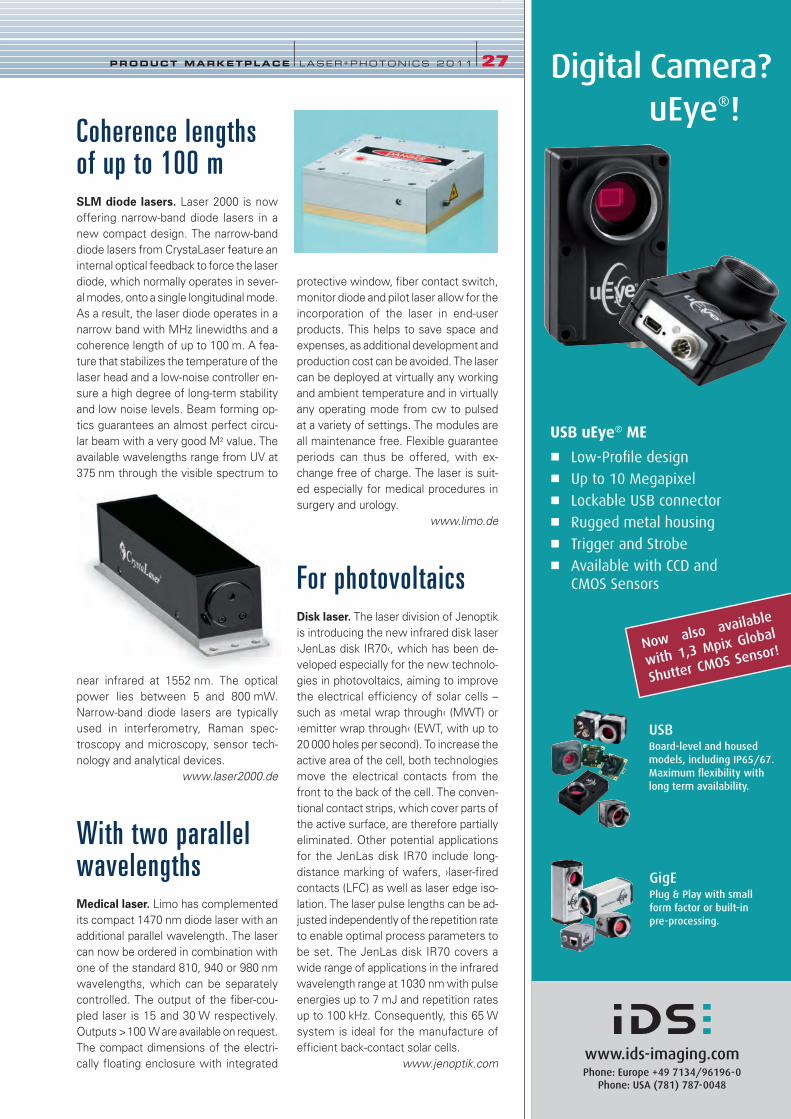
Coherence lengthsof up to 100 m SLM diode lasers. Laser 2000 is now
offering narrow-band diode lasers in a
new compact design. The narrow-band
diode lasers from CrystaLaser feature an
internal optical feedback to force the laser
diode, which normally operates in sever-
al modes, onto a single longitudinal mode.
As a result, the laser diode operates in a
narrow band with MHz linewidths and a
coherence length of up to 100 m. A fea-
ture that stabilizes the temperature of the
laser head and a low-noise controller en-
sure a high degree of long-term stability
and low noise levels. Beam forming op-
tics guarantees an almost perfect circu-
lar beam with a very good M2 value. The
available wavelengths range from UV at
375 nm through the visible spectrum to
near infrared at 1552 nm. The optical
power lies between 5 and 800 mW.
Narrow-band diode lasers are typically
used in interferometry, Raman spec-
troscopy and microscopy, sensor tech-
nology and analytical devices.
www.laser2000.de
With two parallelwavelengths Medical laser. Limo has complemented
its compact 1470 nm diode laser with an
additional parallel wavelength. The laser
can now be ordered in combination with
one of the standard 810, 940 or 980 nm
wavelengths, which can be separately
controlled. The output of the fiber-cou-
pled laser is 15 and 30 W respectively.
Outputs >100 W are available on request.
The compact dimensions of the electri-
cally floating enclosure with integrated
protective window, fiber contact switch,
monitor diode and pilot laser allow for the
incorporation of the laser in end-user
products. This helps to save space and
expenses, as additional development and
production cost can be avoided. The laser
can be deployed at virtually any working
and ambient temperature and in virtually
any operating mode from cw to pulsed
at a variety of settings. The modules are
all maintenance free. Flexible guarantee
periods can thus be offered, with ex-
change free of charge. The laser is suit-
ed especially for medical procedures in
surgery and urology.
www.limo.de
For photovoltaicsDisk laser. The laser division of Jenoptik
is introducing the new infrared disk laser
›JenLas disk IR70‹, which has been de-
veloped especially for the new technolo-
gies in photovoltaics, aiming to improve
the electrical efficiency of solar cells –
such as ›metal wrap through‹ (MWT) or
›emitter wrap through‹ (EWT, with up to
20 000 holes per second). To increase the
active area of the cell, both technologies
move the electrical contacts from the
front to the back of the cell. The conven-
tional contact strips, which cover parts of
the active surface, are therefore partially
eliminated. Other potential applications
for the JenLas disk IR70 include long-
distance marking of wafers, ›laser-fired
contacts (LFC) as well as laser edge iso-
lation. The laser pulse lengths can be ad-
justed independently of the repetition rate
to enable optimal process parameters to
be set. The JenLas disk IR70 covers a
wide range of applications in the infrared
wavelength range at 1030 nm with pulse
energies up to 7 mJ and repetition rates
up to 100 kHz. Consequently, this 65 W
system is ideal for the manufacture of
efficient back-contact solar cells.
www.jenoptik.com
PRODUCT MARKETPLACE l LASER+PHOTONICS 2011 l27
26-27_LPX_Produkte_LPX11 15.12.2010 17:39 Uhr Seite 27

MARION LANG
WILHELM KAENDERS
Increasing performance requirements in astronomy have
led to the development of telescopes or multi-telescope
systems with ever larger primary mirrors (diameters of
up to 30 m). Known as ›Extremely Large Telescopes‹ (ELTs),
they are capable of resolving ever finer details of the night
sky. However, the actual resolution achieved by earth-bound
telescopes is well below the theoretical resolution of a few
tens of milli-arcseconds. The reason for this is the dynam-
ics of the earth’s atmosphere – turbulences between layers
with different temperatures lead to a continual and dynam-
ic distortion of the wavefronts arriving from the objects being
observed.
To circumvent these atmospheric issues, space telescopes
such as the Hubble telescope were developed. However, not
only are these systems extremely expensive, the mirror
diameter that can be implemented is limited by the maximum
payload that modern rockets can transport into earth orbit.
Adaptive optics
For several years, a technique called adaptive optics has been
employed in earth-bound telescopes in order to increase their
resolution. The technique makes use of a deformable mirror in
the telescope’s beam path to introduce an additional and
dynamic wavefront change designed to complement (negate)
the fluctuating wavefront deformation introduced by the
atmosphere. With actuators on the rear of the mirror making
adjustments at up to 1000 times per second, the result is a
significant increase in the spatial resolution of the telescope.
Appropriate reference objects for adaptive optics are ›natural
guide stars‹, or, as these are only available to a limited extent,
so-called ›laser guide stars‹ (LGSs). These are artificially gen-
erated ›stars‹ that act as a point-like light source in the earth’s
outer atmosphere. The light emitted by a LGS is subjected to
the same deformation as that originating from astronomical
objects. Adaptive optics reproduces the image of the guide star
as a point object on the detector, and in doing so simultane-
ously corrects the wavefront distortion for light emanating from
astronomical objects on the same line of observation.
28 l LASER+PHOTONICS 2 0 11 l LASER TECHNOLOGY
Reaching for the stars NARROW-BAND TUNABLE and highly amplified diode lasers for next-
generation large telescopes. For controlling adaptive optics in large telescopes,
so-called ›laser guide stars‹ will be used. Combining a wavelength-stabilized diode
laser with a Raman fiber amplifier and efficient frequency doubling yields tunable,
narrow-band, diffraction-limited continuous wave laser light, with an output
power of more than 20 W. This ›guide star‹ laser enables ground-based astronomical
observations with ten times higher resolution than with the Hubble telescope.
1 Future applicationof the SodiumStar:The narrow-bandtunable diode laserexcites sodium atomsin the mesosphere.The resulting point-like beam spot acts asa reference for theadaptive optics of thetelescope (Image: G. Hüdepohl/ESO)
28-31_LPX110079_LPX11 15.12.2010 17:44 Uhr Seite 28

Generating artificial stars
Sodium atoms are present in the mesosphere, roughly 90 to
110 km above the earth’s surface. These atoms can be reso-
nantly excited by use of a suitable laser, and it is the resulting
fluorescence signal that is used by the adaptive optics system
(Figure 1). In the past, the sodium wavelength has been
generated using dye lasers or sum frequency mixing of solid
state lasers. However, these lasers are either somewhat
cumbersome to operate, or require continuous and intensive
maintenance, respectively. By contrast, a compact, robust
system has now been developed – termed ›SodiumStar‹ – that
generates the required output at the resonant wavelength of
the sodium D2
line, all with higher efficiency, less complexity
and at lower cost (Figure 2).
The operational requirements for guide star lasers are very high.
In order to achieve a sufficiently strong fluorescence signal,
they must provide very high power levels at the sodium wave-
length of 589 nm. Their linewidth may not exceed 5 MHz and,
because of the hyperfine structure of sodium, it must be pos-
sible to fine-tune their frequency. Besides the high requirements
in terms of optical beam quality (TEM00
), the optomechanics of
the laser must also be able to cope with extreme demands.
Reliability under adverse conditions
As a consequence of light pollution, large telescopes are
usually installed in very remote locations and at high altitude.
2 Development of the 20 W laser with TEM00 at 589 nm and alinewidth of less than 5 MHz
3 New flexure design for the ›pro‹ technology
V
LASER TECHNOLOGY l LASER+PHOTONICS 2011 l29
28-31_LPX110079_LPX11 15.12.2010 17:44 Uhr Seite 29

For example, the ›Very Large Telescope‹ belonging to the
European Southern Observatory (ESO) is located on Cerro
Paranal (Chile) at 2600 m above sea level, while the telescopes
on Mauna Kea in Hawaii are located at 4000 m. Cerro Paranal
is also located in an area at risk to earthquakes. This brings
additional requirements in terms of stability and safety, as the
system must be able to remain functional while withstanding
earthquakes up to magnitude 8 on the Richter scale.
The temperature range in which the laser is operated ranges
from -8 to +20°C. The temperature of the outer skin of the laser
may only differ from the ambient temperature by a maximum
of 1.5°C. This places major demands on the laser cooling
system, in particular as fans may not be used for cooling and
convective cooling at high altitude is very inefficient.
The laser head is installed adjacent to the primary mirror of the
telescope. Because obser-
vation time is very expen-
sive, the laser must be
ready for use at all times. In
order to correct misalign-
ment over long time scales,
remote-controlled industri-
al servo motors have been
incorporated into the sys-
tem. And, if the laser
should fail, a modular design enables straightforward
replacement of individual components.
During operation the laser head swivels and rotates along with
the telescope. Thus, considerable attention needs to be paid
to proper function and beam steering for a variable gravitation-
al vector. While short overall beam paths reduce sensitivity to
vibrations and temperature changes, milling the entire laser
head from a single block helps enhance overall mechanical
stability.
20 W power output at 589 nm
thanks to ›pro‹
Toptica’s SodiumStar uses established ›pro‹ technology to meet
these demanding stability requirements. Originally conceived
for scientific laser applications, the pro design was developed
to achieve maximum stability against vibrations, acoustic noise
and temperature changes, at the same time guaranteeing
reliable and optimized hands-off operation. It features a revised
optomechanical concept, making use of innovative flexures and
a monolithic design (Figure 3), and has already been success-
fully implemented in many widely-used laser systems (for
example, in ›DL pro‹ and ›DL SHG pro‹). Another innovation is
the use of special mirror holders with a totally new opto-
mechanical concept. These patent-pending mirror holders were
designed using finite element methods (FEM) and are based
on non-creep flexures with pretensioned springs.
A grating-stabilized diode laser at a wavelength of 1178 nm
serves as master oscillator in the SodiumStar. Both ›distributed
feedback‹ (DFB) laser diodes as well as conventional external
cavity diode lasers (ECDLs) can be used. Revised opto-
mechanics for ECDLs help these systems achieve improved
mode-hop free frequency tuning with maximum stability. For
example, pretensioned flexures give the resonator much greater
rigidity and thus increase the acoustic resonance frequency of
the system to over 3.5 kHz. Coarse and fine-tuning of the wave-
length have been decoupled, hence it is now possible to tune
the wavelength over a greater range without the need for
readjustment. A virtual pivot point for the grating outside of the
mechanics allows mode-hop free fine tuning of the frequency
over a range of more than 50 GHz.
The narrow band seed laser is amplified to more than 35 W
(Figure 4) by a special Raman fiber amplifier (RFA). Via the
process of stimulated Raman scattering an RFA generates a
high power signal out of the low power seed signal. However,
in the past this process was associated with an increase in
linewidth. Recently, the ESO laser group achieved a major break-
through, having developed a method that allows narrow band
Raman amplification. This Raman fiber amplification technique
has been licensed by Toptica and was further developed for use
in the SodiumStar in cooperation with the Canadian company
MPB Communications.
Following the amplifier, the laser light has to be frequency
doubled to reach the sodium resonance wavelength at 589 nm.
For the design of the SHG resonator (Figure 5), Toptica’s pro
30 l LASER+PHOTONICS 2 0 11 l LASER TECHNOLOGY
5 The SHG unit ofthe SodiumStar hasa monolithic design,making it extremelyresistant to vibra-tions. The novel mir-ror holders arebased on preten-sioned flexures
TOPTICA Photonics AG 82166 Gräfelfing/Munich,
Germany
Tel. +49 (0)89 85837-0
Fax +49 (0)89 85837-200
www.toptica.com
CONTACT
4 Schematic of the SodiumStar
28-31_LPX110079_LPX11 15.12.2010 17:45 Uhr Seite 30

philosophy has again been consequently applied. The novel
monolithic resonator is actively stabilized with respect to
temperature and length. Furthermore, it is dust proof, as any
contamination inside the resonator would cause catastrophic
damage to the optics at the laser intensities present inside the
resonator.
Applications beyond the stars
The developments resulting from this project will also benefit
other products. For example, the ›DL RFA SHG pro‹ has been
developed based on the narrow-band RFAs (Figure 6). With a
linewidth of <1 MHz at an output power of 2 W, the system
can be used for spectroscopy and cooling of sodium atoms.
The oscillator of this system is a ›DL100/pro design‹ laser.
Beyond that, RFAs enable the realization of high-power con-
tinuous wave lasers in a very compact format, at any wave-
length between 515 and 620 nm and with tens of watts output
power. These are set to be realized in the coming years in con-
junction with leading customers.
Summary
The SodiumStar is a system that meets all the ESO require-
ments for a guide star laser. The combination of grating-stabi-
lized diode lasers with an RFA and subsequent frequency
doubling results in a narrow-band tunable diffraction-limited
laser with an output power of more than 20 W at 589 nm. A
revised optomechanical design, short free-beam path lengths
and a compact monolithic design benefit aspects such as beam
stability and resistance to external mechanical influences and
temperature changes, as well as safeguarding system per-
formance under harsh conditions. ■
Dr. Wilhelm Kaenders is co-founder and director of Toptica Photonics.
In particular, he is responsible for developing new areas of business for
the company. Dr. Marion Lang is a physicist and works as technical
marketing manager at Toptica. She is responsible for the content and
technical aspects of the company's publications.
LASER TECHNOLOGY l LASER+PHOTONICS 2011 l31
6 The innovative RFA technology is also implemented in theDL RFA SHG pro. The system has an output power of more than 2 W and a linewidth of <1 MHz and is ideally suited forspectroscopy or laser cooling of sodium atoms
Landstrasse 16 I Postfach I FL-9496 BalzersTelefon +423/ 388 11 50-53 I Fax +423/ 388 11 55E-Mail [email protected] I www.filtrop.com
FILTROP AG –Development, manufacturing and supply of :
� OpticsOptical F i l ters I Optical Coatings I OpticalComponents I Optical Raw Materials
� Wet-chemical CoatingsSol-Gel-Nanocomposite Coatings I FluorpolymerCoatings I Decorative Coatings
� Small Tubes and CapillariesFor use in Autosampling, Automatic Dispensing,In-Vitro Measurements, Cl inical Chemistry,Chromatography, Dental Industry, Human Medecine Gr
afik
SiR
up
FILTROP AG –Your Supply-Chain!
28-31_LPX110079_LPX11 15.12.2010 17:45 Uhr Seite 31
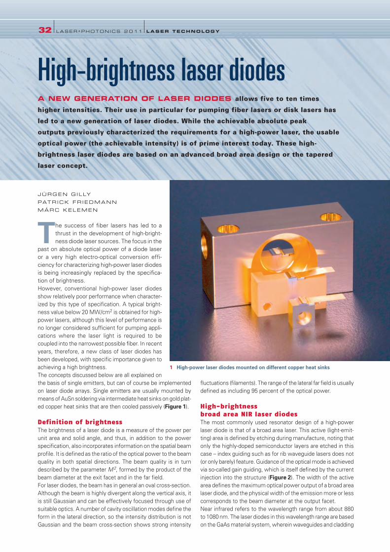
JÜRGEN G ILLY
PATR ICK FR IEDMANN
MÁRC KELEMEN
The success of fiber lasers has led to a
thrust in the development of high-bright-
ness diode laser sources. The focus in the
past on absolute optical power of a diode laser
or a very high electro-optical conversion effi-
ciency for characterizing high-power laser diodes
is being increasingly replaced by the specifica-
tion of brightness.
However, conventional high-power laser diodes
show relatively poor performance when character-
ized by this type of specification. A typical bright-
ness value below 20 MW/cm2 is obtained for high-
power lasers, although this level of performance is
no longer considered sufficient for pumping appli-
cations where the laser light is required to be
coupled into the narrowest possible fiber. In recent
years, therefore, a new class of laser diodes has
been developed, with specific importance given to
achieving a high brightness.
The concepts discussed below are all explained on
the basis of single emitters, but can of course be implemented
on laser diode arrays. Single emitters are usually mounted by
means of AuSn soldering via intermediate heat sinks on gold plat-
ed copper heat sinks that are then cooled passively (Figure 1).
Definition of brightness
The brightness of a laser diode is a measure of the power per
unit area and solid angle, and thus, in addition to the power
specification, also incorporates information on the spatial beam
profile. It is defined as the ratio of the optical power to the beam
quality in both spatial directions. The beam quality is in turn
described by the parameter M2, formed by the product of the
beam diameter at the exit facet and in the far field.
For laser diodes, the beam has in general an oval cross-section.
Although the beam is highly divergent along the vertical axis, it
is still Gaussian and can be effectively focused through use of
suitable optics. A number of cavity oscillation modes define the
form in the lateral direction, so the intensity distribution is not
Gaussian and the beam cross-section shows strong intensity
fluctuations (filaments). The range of the lateral far field is usually
defined as including 95 percent of the optical power.
High-brightness
broad area NIR laser diodes
The most commonly used resonator design of a high-power
laser diode is that of a broad area laser. This active (light-emit-
ting) area is defined by etching during manufacture, noting that
only the highly-doped semiconductor layers are etched in this
case – index guiding such as for rib waveguide lasers does not
(or only barely) feature. Guidance of the optical mode is achieved
via so-called gain guiding, which is itself defined by the current
injection into the structure (Figure 2). The width of the active
area defines the maximum optical power output of a broad area
laser diode, and the physical width of the emission more or less
corresponds to the beam diameter at the output facet.
Near infrared refers to the wavelength range from about 880
to 1080 nm. The laser diodes in this wavelength range are based
on the GaAs material system, wherein waveguides and cladding
32 l LASER+PHOTONICS 2 0 11 l LASER TECHNOLOGY
High-brightness laser diodes A NEW GENERATION OF LASER DIODES allows five to ten times
higher intensities. Their use in particular for pumping fiber lasers or disk lasers has
led to a new generation of laser diodes. While the achievable absolute peak
outputs previously characterized the requirements for a high-power laser, the usable
optical power (the achievable intensity) is of prime interest today. These high-
brightness laser diodes are based on an advanced broad area design or the tapered
laser concept.
1 High-power laser diodes mounted on different copper heat sinks
32-35_LPX110085_LPX11 15.12.2010 17:48 Uhr Seite 32

layers are composed of AlGaAs and
the active (light-emitting) layer
consists of InGaAs. The specific
emission wavelength can be set by
adjusting the indium content in the
InGaAs semiconductor layer.
The brightness is determined as indi-
cated above by the inverse product of
emission area width and far-field di-
vergence. To cater to the need for
high-brightness devices, the emission
width of broad area laser diodes has
thus been consequently reduced in
recent years from 200 to 150, and
down to the 100 µm prevalent today.
However, a major disadvantage of the
broad area design is that a reduction
of the emission width (while keeping
other resonator dimensions constant)
is always accompanied by an expan-
sion of the lateral far field divergence
with increasing operating current. The
main cause of this issue is the reduced ability to dissipate the
heat generated by losses within the cavity.
Thus, in order to satisfactorily increase the brightness of broad
area laser diodes, then, in addition to reducing the emission area
width, it is also necessary to prevent a rapid thermally-induced
growth of the lateral far field beam profile. This requirement
can be met by utilizing the longest possible resonators, which
allow for better heat dissipation over a larger area when com-
pared to shorter resonator lengths. At the same time, the total
electro-optical efficiency must remain at a high level so as to
minimize power loss and thus the amount of heat produced.
Long resonator designs in combination with the highest pos-
sible electro-optical efficiency can only be realized by vertical
laser designs with very low internal losses. Internal losses refer
LASER TECHNOLOGY l LASER+PHOTONICS 2011 l33
2 Schematic diagram of a diode laser with a broad area laser geometry
© LASER+PHOTONICS
Tel. +41 (0)31 712 01 01 (Region Bern)[email protected]
laser-electronics customised solutions
LaserDiodeDrivers
ronics d solutions
www.meerstetter.chLasers made in Europe –For worldwide photonics applications
LASOS Lasertechnik GmbHCarl-Zeiss-Promenade 10, 07745 Jena, [email protected] · www.lasos.com
Our Standard for your OEM-ApplicationDiode-pumped solid state lasersLasNova 50 and 60 series
• Up to 100 mW at 532 nm
• Up to 75 mW at 561 nm
• Single frequency operation
• Designed for long life, low noise and high stability
• Most qualified for fluorescence imaging applications and biophotonics instrumentation
25. – 27. January 2011
The Moscone Center, Booth 1331
San Francisco, California, USA
V
32-35_LPX110085_LPX11 15.12.2010 17:48 Uhr Seite 33

to the loss of charge carriers in the semiconductor layers that
are then no longer available for light output. Specific doping
strategies are also requisite and, similarly, an appropriate choice
for the semiconductor layers can help optimize the heat dissi-
pation within the diode laser. All of these requirements place
very high demands on the capabilities of the (molecular beam)
epitaxy system used, and it is for this reason that the types of
semiconductor laser structure available today are very much
dictated by the type of epitaxy system used for their manu-
facture.
Finally, and supplementary to optimizing the heat dissipation by
extending the resonator length, growth of the lateral far field
profile with increasing operating current can also be reduced
by adopting appropriate process steps during manufacture.
Another major hurdle for increasing brightness results from the
limited power density offered by the currently available facet
coatings. For a desired optical power output (for example, 10 W),
the emission area width is a result of the compromise between
the requirement for high brightness and the need to achieve
sufficiently long component lifetime by avoiding excessive
optical power density through the facet coating.
The overall result is that laser diodes with resonator lengths
between 3 and 5 mm and efficiencies of 55 to 65 percent allow
a sufficiently high brightness to be achieved for most fiber laser
pump applications. A brightness of about 100 MW/cm2 is ob-
tained, for instance, in a broad area laser with an emission area
width of 100 µm and a resonator length of 5 mm, delivering a
lateral far field divergence of less than 8° at an optical power
of 10 W (Figure 3). This represents a five-fold increase in bright-
ness compared to conventional broad area laser diodes.
Tapered laser diodes
To summarize the above case for broad area laser diodes, their
brightness is limited principally by the facet technology and the
emission area width, the thermally-induced expansion of the
lateral far field and the capabilities of the epitaxy system.
Many of these limitations can be circumvented with the concept
of the tapered laser diode, a structure that consists of two
components that have been monolithically integrated as a
MOPA structure onto a single chip. The so-called ridge section
is formed by a single-mode laser diode that serves as the
oscillator (seed laser). Moving away from the seed laser (with
a typical width of 3 µm), the following tapered structure opens
out (as a consequence of the taper angle over the length of the
gain channel) to a width of several hundred micrometers at its
output facet. The input power of sev-
eral tens of mW can thus be boost-
ed to optical powers of several watts
(Figure 4). Through suitable choice
of the design and an appropriate epi-
taxy system, then, currently avail-
able tapered laser diodes exhibit the
same degree of homogeneity in
their electro-optical and spatial beam
characteristics as the aforemen-
tioned high-brightness broad area
lasers, with these characteristics
remaining constant right across a full
production wafer.
Contrary to a broad area laser, the
minimum beam width is not deter-
mined by the width of the (tapered
section’s) output facet, but by the
width of the ridge section – the re-
sult is a beam width 25 times less
than comparable broad area lasers
of same optical power. Additionally,
the lateral far field is determined by the angle of the tapered
section, so that, for example, an angle of 4° results in a far field
divergence of 12°.
Because of the angle of the tapered section, an increase in
power output can be easily realized by simply extending the
length of the tapered section and thus widening the output
facet. The minimum beam width remains constant, so too the
lateral far field and thus also the beam quality. In this instance,
the facet coating no longer plays a limiting role as for broad
area laser diodes.
However, one disadvantage of this concept lies with the astig-
matism that is introduced, an aspect that must be taken into
34 l LASER+PHOTONICS 2 0 11 l LASER TECHNOLOGY
4 Schematic diagram of a diode laser with a tapered laser geometry
© LASER+PHOTONICS
3 Optical power and lateral far field divergence for a high-brightness broad area laser
© LASER+PHOTONICS
32-35_LPX110085_LPX11 15.12.2010 17:48 Uhr Seite 34

account in the design of the optics to be used. Astigmatism
refers to the difference between the position of minimum
beam width along the lateral and vertical beam directions. In
a broad area laser, both minimum beam widths lie on the emis-
sion facet – a result of the symmetrical geometry – and the
astigmatism is correspondingly zero. However, for a tapered
laser, the minimum beam width in the lateral beam direction
lies within the structure. The exact position and thus the degree
of astigmatism is determined by the length of the tapered
section and the corresponding refractive index of the semi-
conductor layers used. As the effective refractive index also
depends on the temperature and the operating current, astig-
matism changes upon modifi-
cation of the parameters.
Depending on the tapered
laser design, optical output
powers from 5 to 10 W with
nearly diffraction-limited beam
quality have already been
demonstrated in practice. A
brightnesses of 200 MW/cm2
is more or less standard, while record values of over
600 MW/cm2 are possible (Figure 5).
Summary
A new generation of high-power laser diodes provides five to
ten times higher optical power densities than conventional
laser diodes and are thus particularly well suited for pumping
applications. These laser diodes are based either on an ad-
vanced broad area design or a tapered laser concept. While
the broad area design is increasingly limited in its brightness
by the requirements on semiconductor technology and facet
coating, tapered laser designs facilitate much higher bright-
ness but also place higher demands on the subsequent opti-
cal design needed for collimation. ■
Dr. Marc Kelemen is partner and Managing Director, while JürgenGilly and Patrick Friedman are responsible for the development work
in the field of high-brightness laser sources at m2k-laser.
LASER TECHNOLOGY l LASER+PHOTONICS 2011 l35
5 Optical power and beam quality of a tapered laser
© LASER+PHOTONICS
m2k-laser GmbH 79108 Freiburg, Germany
Tel. +49 (0)761-5158-7370
Fax +49 (0)761-5158-7376
www.m2k-laser.de
CONTACT
Small Size. Sweet Deal!
www.baslerweb.com/ace
Ground-breaking price starting at 299 Euro Gigabit Ethernet interface with PoE VGA to fi ve megapixels Selected high-quality CCD sensors and CMOS sensors
Strawberry Peppermint Power over Ethernet
299,-
click. see. smile!
32-35_LPX110085_LPX11 15.12.2010 17:48 Uhr Seite 35
Fresnel Optics GmbHFlurstedter Marktweg 13
99510 Apolda
Germany
Phone +49 (0)3644 5011-0
Fax +49 (0)3644 5011-50
www.fresnel-optics.de
Fresnel Optics GmbH – Our expertise foryour successFresnel Optics GmbH, part of Reflexite Ener-
gy Solutions, is a market leader in the design
and fabrication of plastic micro- and nanos-
tructured optical components for the lighting,
solar power, instrumentation and display in-
dustries. Our customized and standard com-
ponents include optics and lenses that en-
hance architectural lighting, solar concentrator
lenses and lens arrays, optical light enhancing
films and a variety of custom designed com-
ponents that improve the performance and ef-
ficiency of of your optical system.
Our Capabilities– Profound experience in optical and me-
chanical design
– Precision mastering (diamond turning, fly-
cutting, linear ruling, laser writing)
– State-of-the-art tool replication (electro-
forming and plating)
– Precision polymer replication (compression
molding, embossing, injection molding,
polymer-on-glass processing)
– Custom finishing (trimming, printing)
– Product enhancement processes (AR-struc-
tures/coatings, aluminum and hard coating,
interference layer)
– Subassembly processes
– Final inspection (standard metrology, cus-
tomized measuring systems)
Our Products– Fresnel lenses
– Fresnel cylinder lenses
– Fresnel prisms and beam splitters
– Micro-lens arrays
– Hybrid optics such as Silicone-on-Glass
(SOG) lens parquets for CPV applica-
tions
36 lCOMPANY PROF ILE
COMPANY PROF ILE
miCos – step in to the futureFounded in 1990 miCos GmbH is now devel-
oping, manufacturing and selling state-of-the-
art systems in the range of micropositioning.
Since 6 years miCos started to develop multi-
axes systems like a hexapod. These devices
have the great advantage that the turning
(Pivot) point can be varied by software. Stacked
axes are on the contrary fixed in the turning
point and have the specific problem that yaw
and pitch errors are dominating the accuracy
of the adjustment. The new designed Space-
fab generation can be more compact and en-
ables to adjust 3 rotations with 10° and 3 trans-
lations with 25 mm. The high dynamic move-
ment is resulting in short processing times.
The repeatability is 1 µm and resolution is less
than 50 nm. The modular design with standard
axes gives the chance to create new space-
fabs for specific applications with different
travels also in other pressure and tem-
perature ranges, f.e. 77K or UHV.
miCos is developing linear and ro-
tary stages with travel ranges
from 2 mm to 1 meter and reso-
lutions down to
2 nm with design
and quality of highest
performance. The new MAC|PhotonX
product line contents educational laser kits and
the optical benches MOSKITO and Albatros.
In telecommunication, semiconductor indus-
try, lasertechnology , biotechnology& health
care, sensors and Space industry multiple
customers profite of the high competence of
miCos.
miCos provides comprehensive customer sup-
port, systems integration and after-sales serv-
ice and is ready to support you in future tech-
nologies in the nanoworld.
miCos GmbHFreiburger Str. 30
79427 Eschbach
Germany
Phone +49 (0)7634 5057-230
Fax +49 (0)7634 5057-393
www.micos.ws
FirmenPortr_LPex2011 15.12.2010 12:24 Uhr Seite 36

COMPANY PROF ILE l37
Docter Optics GmbHMittelweg 29
07806 Neustadt an der Orla
Germany
Phone +49(0)36481 27-0
Fax +49(0)36481 27-270
www.docteroptics.com
Establishments:Docter OpticsExpress Glass Services
Docter Optics GmbH
Str. der Deutschen Einheit 6
07819 Triptis
Germany
Phone +49(0)36481 27-350
Fax +49(0)36481 27-369
Docter OpticsNorth America
Docter Optics, Inc.
1425 West Elliot Road
Suite A-105
Gilbert, AZ 85233
USA
Phone +1 480 844-7585
Fax +1 480 844-7826
Docter OpticsJapan
General Bldg., 2F
No. 25-20,
Sakashita 1-Chome
Itabashi-ku, Tokyo 174-0043
Japan
Phone +81(0)3 3969 3731
Fax +81(0)3 3969 3732
DOCTER OPTICS – Turning Ideas IntoComponents
Docter Optics is an internationally recognized
OEM partner of the optical industry and the
world’s leading supplier of advanced projection
lenses in headlights for automotive applica-
tions. The company’s spectrum of services ex-
tends along the entire value chain: The 420 em-
ployees of the four Docter Optics competence
centers – Precision Glass Components, Opti-
cal Systems, Express Glass Services and Au-
tomotive Solutions – have the experience and
expertise required to take an initial idea to pro-
duction-ready design and deliver customer-
driven solutions.
The company is headquartered in Neustadt an
der Orla, which is located in the heart of Ger-
many’s “Optical Valley.” Docter Optics is also
present worldwide with branch locations and
representative offices in the USA and Japan as
well as a production facility in the Czech Re-
public. First-class references in the areas of
biometrics, machine vision, illumination, solar
energy, printing technology and automotive
applications testify to our customer- and mar-
ket-driven experience and expertise. Docter
Optics also benefits from close cooperation
with partners in research and industry as well
as from active participation in leading technol-
ogy networks for optical professionals. (The
European Community, the Federal Republic of
Germany and the Free State of Thuringia rank
among the sponsors of Docter Optics devel-
opment projects.)
Quality plus efficiency: Precision GlassComponents
Proprietary Docter Optics precision-molding
technology permits exceptionally economical
production of optical components – including
everything from aspheres, arrays and free-form
lenses to light pipes, – for a wide range of ap-
plications even in very large quantities. Cus-
tomers benefit from the services of highly qual-
ified optical designers and process engineers
with the experience and expertise it takes to
design and produce customer-specific optical
components to meet virtually any require-
ments. Customers can order components rang-
ing in size from 5 to 165 mm in diameter. In ad-
dition, Docter Optics has advanced coating fa-
cilities that make it possible to coat all optical
components to customer specifications.
A single-source supplier: Optical Systems
Docter Optics has been involved in the devel-
opment and production of lenses for over 20
years. During that time, the bundled resources
of four business units have made it possible to
achieve unique synergistic effects that have
made Docter Optics a recognized specialist in
the development and production of optical sys-
tems (lenses). A further core competence lies
in the development and production of customer-
specific optomechanical and optoelectronic sub-
assemblies.
In addition, the Docter Optics Optical Systems
competence center supplies industry with its
well-known lenses, including the Tevidon® spe-
cial-purpose CCD and CMOS lenses, the Au-
to-Tessar® reflection-free miniature HDR lens-
es and the Stilar® 2.8/8 super-wide-angle lens
for 1.2” sensor chips.
State-of-the-art: Automotive solutionsfrom Docter Optics
Projection lenses of optical glass for automo-
tive headlights make Docter Optics the in-
dustry leader in this area. Automated produc-
tion technology and the DOC3D® process for
double-sided precision-molded projection
lenses have given Docter Optics a competi-
tive edge that permits short lead times and
precise compliance with customer quality
specifications.
Top-tier services – Express Glass Services
The Docter Optics Express Glass Services
business unit produces semi-finished and fin-
ished products of optical glass, prototypes,
samples and one-of-a-kind components as well
as pre-production or limited series for cus-
tomers worldwide. This business unit also
maintains a large inventory of special optical
glasses of all types.
FirmenPortr_LPex2011 15.12.2010 12:24 Uhr Seite 37

38 lCOMPANY PROF ILE
Visit us at the:
Photonics West 201125 – 27 January 2011
Booth #2210
San Francisco, USA
LASER World of PHOTONICS 201123 – 26 May 2011
Munich, Germany
Contact Information:
ARGES GmbHWerk 4
92442 Wackersdorf
GERMANY
Phone +49 (0)9431 7984-0
Fax +49 (0)9431 7984-300
www.arges.de
ARGES develops and manufactures innovative
laser scanning systems for the deflection and
positioning of laser beams in 1D to 4D appli-
cations in the laser components market. Be-
sides producing a versatile range of standard
scan heads, the portfolio of ARGES is com-
pleted by the development of tailored cus-
tomer- and application-specific solutions, and
the implementation of complete laser sub-
systems for the integration into laser pro-
cessing facilities. With the in-house developed
“InScript©”-Software, and the universal de-
sign of the ARGES System Controller (ASC),
ARGES provides highly integrated scanning
solutions. The ASC is the central device in a
scanning system and combines control and
synchronization of lasers and beam delivery
systems in real-time. The InScript©-Software
allows interactive configuration and remote
monitoring via a network connection. Device
drivers integrate the operation with the exe-
cution of user defined jobs.
ARGES stands for customer-focused technol-
ogy solutions. Thanks to our extensive multi-
industry laser know-how, close collaborations
with all global laser manufacturers and our
overview of the interrelationships within the
laser industry, we are able to serve as a reli-
able and innovative partner to our customers
and assist them in the development of laser-
based processes and machines. Customers
predominately include manufacturers of all-in-
one plant solutions for the semiconductor, elec-
tronic, automotive and photovoltaic industries
as well as the medical technology and the re-
search and development sector. We are in-
volved both in micro and macro laser pro-
cessing.
Technology advice, laser applica-tions and process development
Definite answers to your ideasThe services offered in the develop-
ment and optimization of laser
processes range from individualized
technology advice, pilot studies and
application tests, precision mechani-
cal design, hardware development
(electronic and optical design) and
software and machine control cus-
tomizations right through to prototype
and series production. Our applicationlaboratories which are equipped with a wide
range of laser beam sources and beam
deflection systems as well as a wide variety
of mechanical handling systems provide the
ideal environment for the development of
new technologies. Our in-house MaterialsSciences Laboratory supports the process
development department and, as an impor-
tant element in our trial-accompanying quali-
ty assurance process, acts as a test and qual-
ification center for reliable laser material pro-
cessing solutions.
Technologies that will put you in the leadOur aim is to respond flexibly to a wide variety
of requirements, implement complex tasks in
a timely manner, reduce innovation timeframes
for our customers, and put them in a leading
position through innovative and revolutionary
technologies.
FirmenPortr_LPex2011 15.12.2010 12:24 Uhr Seite 38

High resolution IR camera. VDS Vosskühler has expand-
ed its infrared camera portfolio with the
›IRC-640GE‹, a high-resolution camera
with 640x480 pixels. The camera is
based on a microbolometer sensor sen-
sitive in the range of 8 to14 µm and is able
to resolve differences in temperature of
less than 80 mK. The necessary image
preprocessing is effected within the
camera. The corrected data are output via
a Gigabit Ethernet interface.
www.vdsvossk.de
Versatile sensor Code reader. The ›FA 46‹ code reader
from SensoPart Industriesensorik com-
bines code reading and object recogni-
tion in a single unit. It reads both 1D bar-
codes and 2D data matrix codes com-
plying with the ECC 200 standard and can
analyze up to five data matrix and/or bar
codes in a search zone, while allowing
any number of search zones to be de-
fined. In the same reading process, it is
also able to identify other object features
such as date imprints or stamps. To do
this, it has three additional detectors for
object detection (pattern recognition,
gray scale and contrast). Thanks to the
integrated position tracking option, codes
and object characteristics can be reliably
detected even if they deviate from the
taught position. According to SensoPart,
the FA 46 is capable of handling complex
automation tasks that previously called
for a clasical image processing system
or the use of several sensors, such as
applications in which several codes have
to be read. The FA 46 consists of a com-
pact camera (45x45x64 mm3) with a dig-
ital signal processor, integrated infrared,
red and white light LEDs, Ethernet and
serial RS 422 interface along with digital
I/O. Besides versions with integrated 6
or 12 mm lenses, a C-Mount version is
also available. The sensor is supplied
complete with the required configuration
and monitoring software.
www.sensopart.de
Halcon 10 Machine vision software. The new
›Halcon 10‹ machine vision software from
MVTec Software has expanded its 3D
vision features. It includes, for example,
a new surface-based 3D matching capa-
bility optimized to identify arbitrarily
shaped 3D objects in long-range images,
and that is suppposed to be particularly
adept at recognizing rounded and edge-
less objects. The new multi-view stereo
capability allows the use of any number
of cameras for detailed 3D reconstruc-
tions. It compensates for occlusions and
facilitates robust robotics applications.
Halcon’s calibration capabilities have been
improved and expanded: a new multi-
view 3D calibration function supports an
unlimited number of cameras. Halcon 10
is now capable of finding 3D primitives in
the image by analyzing 21/2D point plots.
A smart text finder supports segmen-
tation in OCR applications and barcode
reading. The integrated development en-
vironment (IDE) and documentation have
also been improved. www.mvtec.com
PRODUCT MARKETPLACE l LASER+PHOTONICS 2011 l39
Laser based systems and components for research and industry• Lasers & Lightsources• Optics & Components• Test & Measurement
www.laser2000.de
Munich, May 23-26 2011, Hall B1
• Science & Research• Biotechnology• Photovoltaics• Image Processing• Network Technology• Security & Defence
Visit us in 2010:
39-41_LPX_Produkte_LPX11 15.12.2010 17:53 Uhr Seite 39

For extendedrecording times Video system. Mikrotron has launched
a complete high-speed video system for
extended recording times. The ›Motion-
Blitz LTR1‹ (long time recording) comes
as a ready-to-use, complete system in-
cluding a 19-inch rack PC, a compact
1.3 megapixel high-speed CMOS digital
camera from the EoSens-series, Camera
Link frame grabber, Camera Link cable,
and control software. It can produce video
recordings at 506 fps for up to 165 min
at full 1280x1024 pixel resolution.
Recordings can also be made at rates of
up to 30 000 fps with the integrated ROI
function, which allows the stepless ad-
justment of the image area's position,
resolution and recording speed.
The high photosensitivity of 2500 ASA
for monochrome imaging and 2000 ASA
for RGB imaging means the camera can
handle complex requirements while also
minimizing lighting expenses. The
switchable non-linear dynamic range
adjustment delivers dynamics of up to
90 dB and ensures extremely detailed
images even with large contrasts be-
tween dark and light. The integrated
Camera Link interface with a data trans-
fer rate of up to 680 MB/s) enables
images from the camera to be saved on
a PC's hard drive in real-time using a ring
buffer.
www.miktrotron.de
High speed live images Microscope cameras. The Digital Imag-
ing business unit of the Jenoptik Optical
Systems Division has added two new
USB camera types to its ›ProgRes‹ CCD
microscope camera range: the ›ProgRes
SpeedXTcore 3‹ and the ›ProgRes
SpeedXTcore 5‹. These cameras feature a
high live image speed of 17 and 13 fps
(respectively) at the corresponding max-
imum possible resolutions of 2080x1542
and 2580x1944 pixels (also respective-
ly). When maximum resolution is not
requried, even higher frame rates of 30
respective 45 fps are possible. Thanks
to the 2 to 3-fold enhancement of the live
image speed in combination with the high
resolution, specimens can be focused
and positioned more easily and quickly –
a clear advantage in the analysis of
moving objects and routine work in lab-
oratories. Exposure times up to 180 s
ensure optimum captured images, even
under low-light conditions. The maximum
possible color depth is 36 bit. In combi-
nation with a C-Mount connection, the
cameras can be easily connected to any
microscope, computer or notebook via
the USB 2.0 interface.
www.jenoptik.com/os
A powerful package GigE Vision cameras. Kappa presents its
extended GigE Vision camera series
›Zelos‹ as a powerful package with SDK,
easy control software and real-time
recording. All Zelos models are based on
a modular high-performance platform
with 14-bit digitization. The series prom-
ises rugged quality, durability and out-
standing color processing. The camera
models with HDTV, 5 megapixel, WVGA
and VGA offer a variety of features such
as PoE, protection class IP 54 and up to
200 fps. Easy to integrate, the cameras
are suited for a wide range of applications.
Due to their clear signal quality, proper
characterization and precise synchroniza-
tion, the Zelos cameras are also ideal for
3D applications. All Zelos cameras are
offered as a package with the control
software ›KCC Zelos‹ and an SDK. With
the new optional real-time recording, live
sequences (also in high-definition) can be
compressed in real-time at full resolution
and full frame rate and then saved as
high-quality video files.
www.kappa.de
40 l LASER+PHOTONICS 2 0 11 lPRODUCT MARKETPLACE
39-41_LPX_Produkte_LPX11 15.12.2010 17:54 Uhr Seite 40
Full performancewith 240 MB/s Dual GigE Interface. With the new ›Dual
GigE‹ interface, Baumer offers a GigE net-
work solution for the implementation of
cameras with fast sensors and high frame
rates. The new interface doubles the
standard bandwidth to 240 MB/s, sup-
porting the full potential of the Kodak
Quad Tap sensors, which provide excel-
lent image quality and high frame rates
simultaneously. With a transfer distance
of 100 m, the Dual GigE interface offers
all the advantages of the standard GigE
interface. However, the redundant con-
cept of the Dual GigE system provides
better transfer security, ensuring data
transfer and reliable camera operation
even if one of the two Ethernet cables is
disconnected. The industrial ›SXG‹ cam-
eras are the first series Baumer is equip-
ping with the new technologgy. These
offer excellent images with resolutions
from 1 to 8 megapixels and simultaneous
frame rates up to 120 fps. All cameras are
supplied with ›power over the Ethernet‹
(POE) for easy integration.
www.baumer.com/cameras
For quick inspectionIndustrial camera. SVS-Vistek recom-
mends its new ›SVCam EV‹ series for fast
and accurate inspection tasks – available
with DualGigE-Vision or CameraLink out-
put. The dual Ethernet output enables the
1 MP model to speed up to 150 images/s,
for instance. The SVCam-EVO series is
enclosed in a compact housing measur-
ing 50x50x48 mm3 and is offered in 1.2
and 4 MP versions, planned for produc-
tion in the 1st quarter of 2011.
www.svs-vistek.de
PRODUCT MARKETPLACE l LASER+PHOTONICS 2011 l41
Faster cameras Camera driver. IDS presents an updated driver version that expands the range
of functions offered by its new cameras with global shutter CMOS sensors from
e2v. This new 1.3 megapixel global shutter sensor offers excellent light sensitiv-
ity and color fidelity combined with a high frame rate. A fast line mode will thus
be available for the USB
and GigE models UI-1240
and UI-5240, enabling
the sensor to record
image lines at a rate of
12000 per second. The
driver update will also
provide an additional
readout mode that al-
lows up to four regions of
interest (ROIs) to be de-
fined per frame and
transmitted simultane-
ously. The cameras with
e2v sensors are further-
more enhanced by digital scaling, creating reduced images with almost no steps
whilst maintaining the full field of view and enabling a frame rate of 100 fps.
Thanks to the overlap trigger mode, the same frame rates are achieved for
externally triggered images as in live mode. Available in monochrome and color,
the sensor’s global shutter renders these CMOS cameras ideal also for inspec-
tion tasks at high cycling rates and fast-moving objects, for example in bottling,
printing or manufacturing of yardware. www.ids-imaging.de
39-41_LPX_Produkte_LPX11 15.12.2010 17:54 Uhr Seite 41
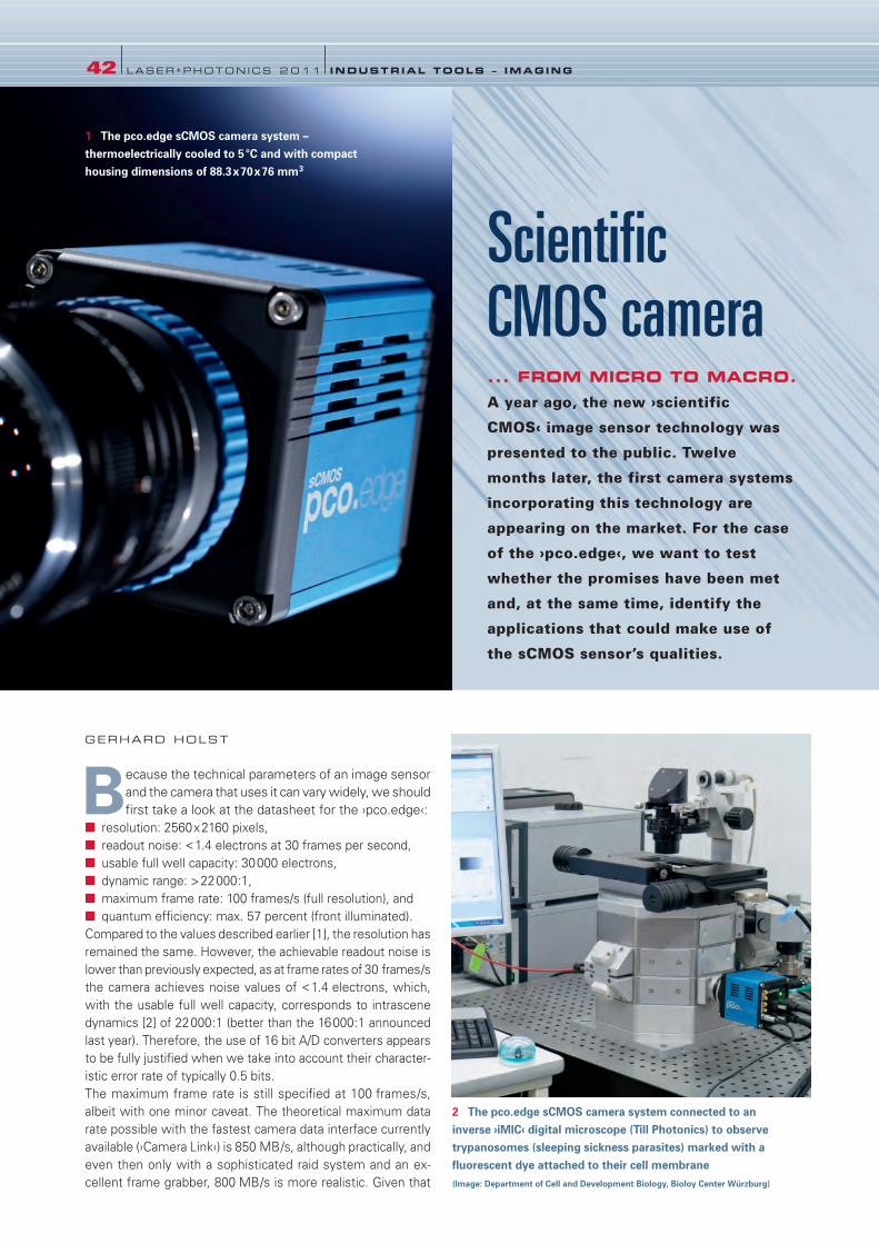
GERHARD HOLST
Because the technical parameters of an image sensor
and the camera that uses it can vary widely, we should
first take a look at the datasheet for the ›pco.edge‹:
■ resolution: 2560x2160 pixels,
■ readout noise: <1.4 electrons at 30 frames per second,
■ usable full well capacity: 30000 electrons,
■ dynamic range: >22000:1,
■ maximum frame rate: 100 frames/s (full resolution), and
■ quantum efficiency: max. 57 percent (front illuminated).
Compared to the values described earlier [1], the resolution has
remained the same. However, the achievable readout noise is
lower than previously expected, as at frame rates of 30 frames/s
the camera achieves noise values of <1.4 electrons, which,
with the usable full well capacity, corresponds to intrascene
dynamics [2] of 22000:1 (better than the 16000:1 announced
last year). Therefore, the use of 16 bit A/D converters appears
to be fully justified when we take into account their character-
istic error rate of typically 0.5 bits.
The maximum frame rate is still specified at 100 frames/s,
albeit with one minor caveat. The theoretical maximum data
rate possible with the fastest camera data interface currently
available (›Camera Link‹) is 850 MB/s, although practically, and
even then only with a sophisticated raid system and an ex-
cellent frame grabber, 800 MB/s is more realistic. Given that
42 l LASER+PHOTONICS 2 0 11 l INDUSTRIAL TOOLS – IMAGING
Scientific CMOS camera ... FROM MICRO TO MACRO. A year ago, the new ›scientific
CMOS‹ image sensor technology was
presented to the public. Twelve
months later, the first camera systems
incorporating this technology are
appearing on the market. For the case
of the ›pco.edge‹, we want to test
whether the promises have been met
and, at the same time, identify the
applications that could make use of
the sCMOS sensor’s qualities.
2 The pco.edge sCMOS camera system connected to aninverse ›iMIC‹ digital microscope (Till Photonics) to observetrypanosomes (sleeping sickness parasites) marked with afluorescent dye attached to their cell membrane (Image: Department of Cell and Development Biology, Bioloy Center Würzburg)
1 The pco.edge sCMOS camera system – thermoelectrically cooled to 5°C and with compacthousing dimensions of 88.3x70x76 mm3
42-45_LPX110073_LPX11 15.12.2010 17:56 Uhr Seite 42

the sCMOS camera can deliver 1.14 GB/s, the actual data trans-
fer rate is ultimately limited by the currently available interface
standards. The net result is that the full frame rate can only be
utilized together with data compression or a reduced dynamic
range. The second limitation, at least compared to the infor-
mation made available last year, lies in the slightly reduced quan-
tum efficiency. The actual specification includes losses from
cover glasses and the slightly lower values attained for the
series production sensors, although the minor drop from 60 to
57 percent is very likely tolerable for most applications. In spite
of this, the sensitivity in the NIR is still significantly higher than
conventional CCD or CMOS image sensors.
On the whole, the pco.edge camera (Figure 1) not only deliv-
ers the promised sCMOS specifications, in some instances the
final performance is actually better. What we now need to
explore is the applications that require all of or a significant
subset of these specifications when addressing their specific
objectives.
Micro – frame rate, noise and sensitivity
According to Prof. M. Engstler, the trypanosome parasites that
cause sleeping sickness are ›ravenous swimmers‹ [3]. In the
blood of the host, these 20 µm long parasites use a character-
istic motion to generate a hydrodynamic flow on their cell
surface that effectively renders the defense mechanisms of
the host useless. This hydrodynamic flow drives the host’s
antibodies back along the parasite membrane and on to the rear
end of the parasite cell. Here the antibodies are passed into the
mouth of the cell, where they are devoured and finally con-
sumed.
Transmitted by the tsetse fly, a huge number of people in Africa
still die of sleeping sickness (30000 new cases per year [Source:
Wikipedia]). Unfortunately, the treatment methods are outdat-
ed and place a significant additional strain on the patient, so
research into more effective and patient-friendly treatment
methods is an important field. These parasites also destroy
entire herds of buffalo and cattle, which, in the corresponding
INDUSTRIAL TOOLS – IMAGING l LASER+PHOTONICS 2011 l43
3 Image details(550x350 pixels) from asequence of imagesshowing the movementof trypanosomes, cap-tured with the pco.edgesCMOS camera systemat a resolution of1120x502 pixels and aframe rate of400 frames/s. The rapidmovement of thetrypanosomes is easilyinterpreted from theintervals between theindividual images
www.leoni-fi ber-optics.com
:
V
42-45_LPX110073_LPX11 15.12.2010 17:56 Uhr Seite 43

tropical lands of Africa, is a cause of significant economic hard-
ship. One potential new method of therapy could be to influ-
ence the motion of the trypanosomes, but this needs to be
studied in greater detail first.
In order to influence the flagellates as little as possible, appro-
priate tagging proteins were used to mark the cell membrane
with a fluorescent dye, and the trypanosomes were then ob-
served in a liquid environment on the slide of an inverse digital
›iMIC‹ microscope (Figure 2) coupled to a sCMOS camera. For
the very first time, image sequences of the characteristic
movement of the fluorescent trypanosomes were captured with
sufficient time resolution. Sequences with 1120x1080 pixels
were captured at 200 frames/s and with 1120x502 pixels at
400 frames/s. A sequence of four (cropped) images can be seen
in Figure 3.
Given the short time intervals between
images, the significant changes in pos-
ture of the two trypanosomes are in-
dicative of how quickly these flagellates
move. The light signals comprise around
100 photons at the brightest locations,
which is of course a very weak signal.
These sequences of images are currently
being studied and processed, particular-
ly in terms of the three-dimensional
characteristics of the movement, and
further investigations will follow.
Macro – NIR sensitivity,
resolution and noise
For several years now, the electro-
luminescence (EL) of solar cells has
been used as a significant parameter in
research and quality assurance. Scien-
tific studies have shown that the areas
of solar cells that do not exhibit EL also
do not make a contribution to the gen-
erated photoelectric current. Solar cell
research is currently engaged in partic-
ular on the proper interpretation and
significance of EL measurements. To produce the EL, a
safe nominal current is applied in flow direction that
mimics the expected photovoltaic current through indi-
vidual solar cells or entire modules. Light with an in-
tensity maximum around 1150 nm in the near infrared
is generated in the cells – nominally outside the sensi-
tivity range of the camera sensor. Nevertheless, the
component of the EL intensity with a wavelength be-
low roughly 1050 nm is sufficient to generate a usable
signal. Until recently, specially optimized CCD cameras
have been used for this task, but they either needed to
utilize pixel binning to produce a sufficiently visible image
or required longer exposure times in the range of 30 to
60 seconds or more.
In addition to the high resolution, the sCMOS image
sensor also has a better quantum efficiency than front-
illuminated CCDs. And unlike the ›deep depletion‹ CCDs,
all of which are illuminated from the rear through the
substrate, there is also no etaloning. Figure 4 shows
the EL for a solar cell module, captured using a special
IR objective from Carl Zeiss. The exposure time was 700 ms,
meaning that the type of EL image capture needed for quality
assurance can be taken easily during manufacture. In Figure 4,
a defect is marked with an arrow. Current research still needs
to provide answers to improve understanding and identify the
significance of the other darker areas.
Aero – frame rate,
dynamic range and resolution
The DLR Institute for Robotics and Mechatronics in Berlin has
been developing aerial reconnaissance systems for some time.
Through the utilization of additional sensors, the absolute
position of the aircraft is very accurately known and it becomes
possible to ensure that adjacent images of a target area always
have at least 90 percent overlap. Sophisticated algorithms can
44 l LASER+PHOTONICS 2 0 11 l INDUSTRIAL TOOLS – IMAGING
4 Electroluminescence image of a solar cell module taken with a pco.edgesCMOS camera system with a 50 mm NIR lens from Carl Zeiss and using anexposure time of 700 ms. The black speck (marked) shows a defective area ofthe solar cell that makes no contribution to the photovoltaic current
5 An aerial photo taken with a pco.4000 CCD (11 megapixels) from an altitude ofapproximately 150 m. One pixel corresponds to a ground resolution of 2 cm, thus the100x100 pixel detail corresponds to an area of 2x2 m2 on the ground. This camera is tobe replaced by two sCMOS cameras, which are more compact and will be able to cap-ture images with improved dynamic range
42-45_LPX110073_LPX11 15.12.2010 17:56 Uhr Seite 44

then be applied to these images to obtain a height profile of the
target area.
At present, high-resolution CCD cameras such as the ›pco.4000‹
(4008x2672 pixels with color sensor) are being used, and that
capture images with sufficient speed (3 frames/s). With this
camera a single pixel corresponds to 2 cm on the ground (Fig-ure 5), achieved at an altitude of around 150 m, and the reso-
lution for the calculated height profile is around 3 cm. The
disadvantages of the pco.4000 include its size and, above all,
the tendency to ›smear‹
images (the stripe-like
artifacts left behind in the
images due to very bright
spots of light in the imaged
scene).
sCMOS cameras with a
color sensor are now to be
integrated into these aerial
photographic systems. Although they only have half the reso-
lution, they produce no smear effects and also have a consid-
erably higher frame rate. In addition they benefit from a better
dynamic range, a more compact format (Figure 1) and they
weigh less. The aim is to improve the resolution of the height
profiles from 3 to 1 cm for this research work. By flying over a
road construction site before, during and after construction, this
kind of system could then be used to determine exactly how
much excavation was actually carried out. Other applications
include creating height models of major population centers, so
that detailed emergency response plans can be formulated, or
determining the exact size and extent of cities in countries
where building activity has not been continuously recorded.
Summary
The original announcement of the sCMOS camera systems
and the significant interest in the performance specifications
prompted a deluge of potential applications in fields ranging
from micro to macro. From microscopy through to aerial photo-
graphy, there is certainly no lack of interest in the capabilities
of the sCMOS image sensor technology. Potential applications
can easily be envisaged that range from super-resolution
microscopy, over DNA analysis and even on to 3D film capture
and 2D stereo image acquisition. The term »scientific CMOS«
also appears to have drawn so much attention that it is
increasingly being used even for lesser performant CMOS image
sensors in order to emphasize their qualities. ■
Literature 1 Laser+Photonics 5 (2009), p.18.
2 The intrascene dynamic range is defined as the ratio of the maxi-
mum fill level to the smallest distinguishable signal level (comparable
to the noise). This dynamic is the customary dynamic range generally
specified for digital camera systems.
3 Department of Zoology I (Cell and Development Biology) at the
Biological Center of the University of Würzburg, in his article in Labor
& More 3 (2010).
Gerhard Holst studied information technology at the RWTH Aachen.
After seven years in the microsensor research group at the MPI for
Marine Microbiology in Bremen, he moved to PCO, where he is now
Head of the science and research department.
INDUSTRIAL TOOLS – IMAGING l LASER+PHOTONICS 2011 l45
Prismastrasse 5CH-9444 DiepoldsauSwitzerlandTel. +41 71 737 74 00Fax +41 71 737 74 10www.zuendoptics.com
Microprisms up
to 0.2 mm in all
desired divergences.
Beam-splitting
cubes from 1 mm.
Graduated filter.
zünd precision optics
Perfection in detailfibre opticsEquipped for the future
PCO AG93309 Kelheim, Germany
Tel. +49 (0)9441 2005-0
Fax +49 (0)9441 2005-20
www.pco.de
CONTACT
42-45_LPX110073_LPX11 15.12.2010 17:56 Uhr Seite 45

For rapid scanning 3D sensors. With its ›CX Compact‹ sen-
sors, Automation Technology is launch-
ing a new generation of detector heads
for high-speed 3D scanning. The high res-
olution sensors are available with a reso-
lution of 2352x1728 pixels and a maxi-
mum profile frequency of 23.5 kHz or
with 1280x1024 pixels and up to
71.5 kHz. These, along with the complete
laser electronics, are built into a compact
and durable anodized aluminum housing
(IP 64/67) that can be adapted to cus-
tomer-specific demands. Both Camera-
Link and the GigE Vision standard
interfaces are available. The CX sensors
support the GenICam protocol, making
them easy to integrate. The Gigabit
Ethernet version is also available as a
smart camera with a 1 GB image memo-
ry. According to the manufacturer, the
sensors provide outstanding depth of
field and image intensity and are able to
scan even materials and surfaces with
non-homogeneous reflectivity properties.
The sensors can be combined with a
wide range of commercially available
image processing tools.
www.automationtechnology.de
Compact and fast CMOS cameras. The new, small, fast
and high resolution ›ace‹ cameras from
Basler use the new CMOS sensors from
Cmosis. They have resolutions of 2 and
4 megapixels and achieve up to 340 and
180 fps, respectively. With a global shut-
ter and Camera Link interface, these
cameras are suited for a wide range of
applications – especially high-throughput
applications. Features such as trigger or
flash support via separate I/O ports and
optional ›Power over Camera Link‹
(PoCL) functionality facilitate hardware
installation. Thanks to GenICam support,
all camera properties can be flexibly
adapted via software commands. Ac-
cording to Basler, these highly compact
cameras – with a footprint of 29x29 mm2
– also boast an impressive price-
performance ratio. In late 2011, Basler
will also offer the ace Cmosis cameras
with a GigE interface.
www.baslerweb.com
46 l LASER+PHOTONICS 2 0 11 lPRODUCT MARKETPLACE
Your Partner in Lighting Technology
SphereOptics GmbHBergstr. 36 · D-88690 Uhldingen-Mühlhofen
Phone +49 7756 929 96 66 · [email protected]
Zenith Diffuse Refl ectance Materials
Sphere-based Light Measurement Technology
Near-fi eld/Far-fi eld Goniophotometers & CCD-based Light Measurement Technology
Remote Sensing & Hyperspectral Imaging
With 8192 pixels Color line scan camera.Vistas is extending its
›CLISBee-S‹ CMOS range
of line scan cameras to
include a color version, the
›XCM2740MLC‹, with
serial RGB pattern in
which the line length of
8192 pixels at 7x7 µm2
provides a color resolution
of 2730 x RGB pattern.
The pixel frequency is
120 MHz at a scanning
rate of 14 kHz and 24 bit
RGB resolution. Data is transmitted via a CameraLink inter-
face. Integrated correction functions are used for pixel
correction, FPN and PRNU minimization and to correct for
non-uniform illumination and lens vignetting. Thanks to an
adjustable characteristic curve, it has a specified dynamic
range of 106 dB. The offset and gain are individually pro-
grammable for each RGB color channel. Gain is precisely
adjustable in 0.0039 dB increments. The camera, in a com-
pact metal housing measuring 80x120x65 mm3, is supplied
with the standard ›M72x075‹ lens connection. A version
with a Nikon F–Mount adapter is also available but its reso-
lution is limited to 4096 pixels or 1365 x RGB patterns.
www.vistas-gmbh.de
46-47_LPX_Produkte_LPX11 15.12.2010 17:57 Uhr Seite 46

Pre-calibrated 3D Area Sensor. VRmagic presents a 3D
area sensor based on digital stripe light
projection that supplies pre-calculated 3D
data records for industrial image pro-
cessing. The ›AreaScan3D‹ sensor out-
puts the recorded 3D data directly as a
point cloud or a grayscale-coded range
map to the evaluation computer via the
industrial Ethernet interface. The 3D sen-
sor is addressed via a GenICam transport
layer (GenTL), making it compatible with
all image processing libraries and pack-
ages that communicate with a GenTL,
such as Common Vision Blox or Halcon.
The sensor is encased in a robust metal
housing with IP 65 protection, screw-
type standard industrial connectors, a
24 V connection, an Ethernet interface as
well as hardware and software triggers.
It is available with measuring fields rang-
ing from a few millimeters up to a square
meter. It offers a guaranteed accuracy in
the submicrometer to millimeter range,
depending on the measuring field size.
Stripe projection, image recording and
generation of the point cloud are per-
formed in an integrated manner based
on an intelligent camera from VRmagic.
The DLP pico projector from Texas In-
struments and the camera are synchro-
nized with a frequency of 60 Hz. Output
of a complete 3D data record is current-
ly possible with approximately 360 000
individual points per scan.
www.vrmagic-imaging.com
ARM’d with intelligence Intelligent camera. Matrix Vision's new
intelligent camera series ›mvBlueLynx-X‹
uses Texas Instruments’ ›OMAP 3‹
processors with an ›ARM-Cortex-A8‹
core and offer an efficient performance
up to 1 GHz with an additional, separate
DSP. When designing this series for au-
tomation, Matrix Vision deliberately
chose ARM processors as these require
less power and are smaller in size. As a
result, mvBlueLynx-X is able to operate
with 5 W under a full load and is com-
pact in size, measuring 85x55x35 mm3
without lens. The cameras feature a wide
range of interfaces: 100 Mbit LAN, two
USB 2.0 interfaces, RS-232, digital inputs
and outputs, display output as well as
MicroSD card interfaces. A wide range
of global shutter CMOS sensors from
WVGA to SXGA are also available. For the
lens holder, a S-mount is standard, but
C- and CS-mounts are available as an
option. Models with integrated illumina-
tion improve the handling and garantee
image quality. Models with IP 65 protec-
tion are available as well. A ›.NET‹ com-
pliant ›Mono‹ interface allows the devel-
opment and implementation of .NET
based cross platform applications with-
out further compiling.
www.matrix-vision.de
Customizable Telecentric lenses. With its ›TZ Coax‹
series, IB/E provides telecentric meas-
urement lenses for the most demanding
requirements. With reflected light, they
are particularly suitable for inspection of
tiny surface defects such as scratches,
grooves, burrs and dents. On request, the
lenses can also be equipped with variable
aperture, polarizing filter and retarder
plates. IB/E Optics can provide
›OptiBench‹ as a protocol for precise
distortion, MTF and telecentric data. The
TZ Coax series covers scales from 0.5 to
3.00. LED and fiber inputs for coaxial
illumination are available as accessories.
www.ibe-optics.com
PRODUCT MARKETPLACE l LASER+PHOTONICS 2011 l47
46-47_LPX_Produkte_LPX11 15.12.2010 17:57 Uhr Seite 47

48 l LASER+PHOTONICS 2 0 11 l INDUSTRIAL TOOLS – LASER V IBROMETRY
Laser Doppler vibrometry VIBRATION MEASUREMENT WITH LIGHT – simple and versatile. Laser
Doppler vibrometry was originally developed to study the dynamics of mechanical
structures and systems, but has also proved ideal for studying biological structures
and mechanisms.
JÖRG SAUER
HE INR ICH STEGER
ARNO MAURER
Non-contact laser vibrometers are firmly established as
an indispensable method for studying the structural
dynamics of physical and biological systems and for
optimizing the response of mechanical products with respect
to vibration and noise. A laser vibrometer is built around an
interferometer where a laser beam (usually HeNe at 633 nm,
P <1 mW) is divided into a measurement and a reference
beam by a beam splitter. The measurement beam strikes a
point on the vibrating surface, which then scatters light back
to the vibrometer with a shift in frequency and phase due to
the Doppler effect. The returning light is captured by the
vibrometer optics and spatially overlapped with the reference
beam, giving rise to a time-varying interference.
The frequency shift in the measurement beam caused by the
movement of the structure being tested results in a modula-
tion in time of the combined beams’ light intensity. Each time
the measurement point on the vibrating surface moves by a
half wavelength, the intensity of the superposed light com-
pletes a full light /dark cycle. The intensity fluctuation is con-
verted into a corresponding electrical signal by a photodetec-
tor. The frequency fD of these light /dark cycles is proportional
to the speed v of the measured point according to:
fD = 2v/l
Laser vibrometry has almost limitless application possibilities
and is already used in a broad range of fields. It has several
important advantages including efficient and practical meas-
urement setups, extremely accurate vibration measurement,
zero mass loading and suitability to applications where con-
ventional sensors cannot be used.
1 The basic optical principleof a laser vibrometer
48-51_LPX110059_LPX11 15.12.2010 18:01 Uhr Seite 48
Vibrometer types
The fundamental principle of non-contact, non-impinging (or
zero mass loading) and high-resolution optical vibrometry (as
illustrated in Figure 1) is the basis for most standard vibro-
meters as well as for a series of more versatile and special-
ized instruments (Figure 2). For example, the second inter-
ferometer beam, which normally plays the role of the refer-
ence beam, can also be used as a measurement beam. This
enables differential optical measurements that can, for exam-
ple, eliminate ambient vibrations from the measurement data
by overlaying the actual object vibration with the measurement
point data.
Another two-beam concept forms the basis for the in-plane
vibrometer. For an object located within the volume outlined
by two overlapping light beams, vibrations perpendicular to the
principal optical axis can be measured. And then for three over-
lapping beams, as is the case for a 3D vibrometer, the entire
three-dimensional vibration vector can be conveniently evalu-
ated. Finally, the double interferometer detector head of the
rotational laser vibrometer can be used to record the dynamics
of rotating systems, such as on the drive train of a vehicle
during ramp-up tests.
In addition to single-point vibrometry systems (those used to
observe a single point on a vibrating structure), there are more
powerful vibrometer systems, known as scanning vibrometers,
that measure over an en-
tire surface. A scanning
vibrometer is typically a
high-performance all-in-
one combination of inter-
ferometer, precision scan-
ner optics, an integrated
video camera and a pow-
erful data acquisition sys-
tem. Such systems enable vibrometry measurements to be
carried out on vibrating surfaces and structures by automati-
cally scanning the entire surface of the measurement object
with an interactive and flexible user-defined array of meas-
urement spots. The ultimate extension of this approach is the
three synchronously controlled scanning vibrometer detector
heads of a 3D scanning vibrometer, capable of recording 3D
vibration data for complex structures.
Vibration diagnostics
on wind power plants
Wind power turbines must satisfy stringent design require-
ments for the mechanical properties of the components. In
operation, the effect of the wind can induce vibrations that on
larger turbines can lead to dynamic deflections of the tower and
of the rotor blades of up to 1m, at frequencies of several Hz.
The motivation for characterizing the wind power turbines is to
compare, contrast and optimize the simulation models used in
the design and to ensure that the mechanical operation remains
fault-free by promptly identifying the critical material loads and
the corresponding fatigue data. This kind of preventive mainte-
nance or condition monitoring is often carried out using contact
sensors positioned at assorted points throughout the power
train. For example, appropriately placed sensors can provide in-
formation about bearing wear and tear induced by power trans-
mission. For the rotor blades, particularly during operation, a non-
contact optical measurement method is obviously preferable for
practical reasons. Laser vibrometry is non-contact and has the
additional advantage that measurements can be carried out at
a safe working distance and, in ideal situations, without prior
preparation of the measurement points (Figure 3).
Ultrahigh-frequency measurements
on microsystems
Microsystems with ultrahigh-frequency mechanical movements
are often characterized by sub-picometer (pm) displacements
INDUSTRIAL TOOLS – LASER V IBROMETRY l LASER+PHOTONICS 2011 l49
2 Overview of differentvibrometer types. This col-lection of powerful opticalvibration measurementsystems provides userswith an optimum solutionfor almost any measure-ment task
3 Vibration measurement on wind power turbines
Polytec GmbH 76337 Waldbronn, Germany
Tel. +49 (0)7243 604-0
Fax +49 (0)7243 699-44
www.polytec.de
CONTACT
V
48-51_LPX110059_LPX11 15.12.2010 18:02 Uhr Seite 49

in the GHz range. To measure these movements directly and
without contact presents a major challenge for the measure-
ment technology.
A new ultrahigh-frequency vibrometer can now be used to
measure these movements directly at frequencies of up to
1.2 GHz and with amplitudes in the sub-pm range. The meas-
urement is straightforward and non-contact. The software even
allows the vibration to be visualized in slow-motion. Because
of the large frequency bandwidth, this vibrometer is an ideal
tool for studying high-frequency RF-MEMS, while its high
lateral resolution makes the system perfect for studying and
dynamically characterizing devices with short acoustic wave-
lengths, such as surface acoustic wave (SAW) devices or bulk
acoustic wave (BAW) devices. Because of the large speed
measurement range of up to 120 m/s, it is also ideal for preci-
sion characterization of high-performance ultrasonic transduc-
ers (Figure 4).
Product development
in the automotive sector
Optimizing acoustic and vibrational behavior is an important
objective in product development, in particular in the automo-
tive industry, as the dynamic and acoustic properties are key
quality aspects for a vehicle’s ›look and feel‹. In recent years,
non-contact optical measurement technology featuring laser
Doppler vibrometers has become the established tool for ex-
perimental vibration analysis in many applications. The reasons
for this rapid acceptance include its high throughput and accu-
racy, its suitability for even the most difficult, complex or
microscopic measurement tasks, and its ease of use.
In the development of a new motor vehicle, the use of numerical
calculations to predict the vibrational behavior of components,
of assemblies and of the vehicle as a whole has become a stan-
dard procedure and makes a major contribution to optimizing
operational safety and long-term performance. Confidence in
the numerical simulations comes from the comparison of the
predicted model’s response with data obtained experimental-
ly (modal test) on a real component.
Here too, laser vibrometers have become the preferred instru-
ment for capturing experimental data. In particular, laser vibro-
meters exhibit some crucial advantages over mechanical
accelerometers that are mounted to the structures (see below).
3D scanning vibrometers have additional advantages such as
measuring vibrational components along all three axes at each
defined measurement point covering the test object – even
over the entire area of a full vehicle in just a few hours when
combined with an industrial robot.
In experimental modal analysis, a specific broadband force is
transmitted into the structure. To input this tailored force, one
or more electrodynamic vibration generators, known as ›shak-
ers‹, are used. During data acquisition, the vibrometer system
calculates the frequency response function (FRF) between the
force and the vibrometer signal (speed) in a specified frequen-
cy range for each measurement point, which is then saved for
further signal analysis. The operational deflection shapes are
formed from piecing together the individual measurement
points and tying them together temporally and spatially to form
an animation of a geometric model, against frequency or time,
and superimposed over the video image of
the measured object. Standard interfaces are
then used to provide the FRFs for post-
processing using modal analysis software.
When performing modal tests of this nature,
scanning 3D vibrometry provides some key
advantages:
■ quick and easy measurements, even with
a very high density of measurement points,
■ mass loading from an attached sensor,
■ considerably shorter setup time compared
to the time-consuming instrumentation of
the measurement object with accelerom-
eters,
50 l LASER+PHOTONICS 2 0 11 l INDUSTRIAL TOOLS – LASER V IBROMETRY
5 Test setup for determining the modal properties of a 20 m solar sail for NASA
4 Full area measurements on an ultrasound transducer at approximately 105 MHz, measured with a PolytecUHF-120 ultrahigh-frequency vibrometer
48-51_LPX110059_LPX11 15.12.2010 18:02 Uhr Seite 50

■ comprehensive frequency response functions (FRFs) with
high spatial resolution, ideal for correlation with FE models
(›model updating‹, even at high frequencies),
■ full automation of the measurement, including robot support
for large structures, and
■ simultaneous actuation of up to four vibration generators al-
lowing MIMO modal tests.
The user benefits from the extremely high density of meas-
urement points, far superior to that captured by conventional
contact measurement technology, and a reduction in total test
time from weeks down to a few hours.
This innovative dynamic testing methodology with laser vibro-
meters helps understand and optimize the acoustic signature
of disk brake systems. Under certain operating conditions, the
complex dynamics between the brake caliper, pads and disk
can cause intolerable brake squealing, perceived by vehicle
users as an indication of inferior quality. By measuring the
operational vibrational forms with a
3D scanning vibrometer on the brake
test bench, the 3D dynamics can be
properly characterized and under-
stood. These measurements reveal
the interactions between the primary
vibration modes in the plane of the
disk and the secondary modes vi-
brating out of the plane of the disk.
With this information, one can de-
termine which modes are responsi-
ble for the acoustic issues. These
types of measurements can be per-
formed on all substructures of the
braking system, both at rest and in
operation on the test bench.
Aerospace
In the aerospace industry, vibrations are almost always un-
desirable and must be detected quickly and then eliminated. It
is important to catch these vibrations in the design and test
phase and during the manufacturing process as part of quality
control. Typical applications for laser vibrometry include data for
design reviews, characterization of components as part of pro-
duction monitoring and investigation of material fatigue. Meas-
urements on wings, turbine blades and satellites provide data
for modal analyses and finite element validations. Vibrometers
are ideal for measurements on large objects that are difficult to
access with contact methods. As a special example, in Figure 5a test setup for determining the modal properties of a 20 m
solar sail for NASA is shown, along with the measured results
obtained. In order to perform measurements in a realistic
operating environment for the solar sail, the investigations were
carried out in an immense vacuum chamber.
Applications in production monitoring
In industrial production, non-contact optical sensors offer a
range of advantages – extremely precise measurement values,
flexible integration and reliable, low maintenance operation.
They make an important contribution to optimizing processes
and thus to overall profitability.
Structural properties and faults manifest themselves directly in
the dynamic properties of structures and products. Standard
components and assemblies can be characterized in terms of
Eigen frequencies, damping and mode shapes. Appropriate
measurements allow for evaluation and classification of these
properties, enabling a rapid and automized pass/fail selection
of components. For many applications subject to final produc-
tion inspection, laser vibrometers have considerable advantages
over conventional structure-borne sensor technology, such as
mechanical accelerometers. As well as the high-dynamic range
and the large bandwidth of the vibrometers, the non-contact
and therefore massless measurement technology also plays a
critical role.
The production inspection for nebulizer membranes at Pari, one
of the leading manufacturers of aerosol generation systems in
Germany, is a good example. Here, a compact laser vibrometer
is used to perform 100 percent testing of the quality of the
systems during production. Measuring the vibrational behavior
at the aerosol producing membrane – the core of the nebuliz-
er system – goes a long way towards ensuring the final quali-
ty of the aerosol generator as a whole (Figure 6).
Metrology and calibration
As a calibration standard reference, laser vibrometry has the
unique advantage that the measured quantities used to
calibrate vibration sensors can be traced back directly to the
wavelength of the laser light used. And, for the first time,
velocity measurements using laser vibrometers enable the
study of the dynamic behavior of force transducers under
known impact loading.
Summary
Laser vibrometers are an indispensable and reliable tool for
optical vibration measurements in countless applications. The
range of use covers everything from characterization of
microstructures to high-performance, fully automated meas-
urement of entire motor vehicles. Because the method is
non-contact and massless, vibrometry is often the only solu-
tion for very demanding measurement tasks and, in terms of
simplicity and efficiency, is significantly superior to mechanical
measurement technology in many applications. ■
Dr. Arno Maurer is the head of Polytec’s Operative Marketing
department, Jörg Sauer is Polytec’s Product Manager for Laser
Vibrometry and Dr. Heinrich Steger is the head of Polytec’s Strategic
Product Marketing in the Optical Measurement Systems division.
INDUSTRIAL TOOLS – LASER V IBROMETRY l LASER+PHOTONICS 2011 l51
6 Medication nebulizer and the compact laser vibrometer used for testing
48-51_LPX110059_LPX11 15.12.2010 18:02 Uhr Seite 51

MARKET ING OWIS
Resolution and repeatability play an increasingly im-
portant role in positioning tasks in fields such as
microscopy, nanotechnology, semiconductor tech-
nology, quality assurance, photonics and surface process-
ing. Specifically regarding these two key properties, the
performance of the positioning technology utilized is often
subject to very high demands.
To meet these growing demands, positioning stages with dif-
ferent drive technologies are continually being developed and
optimized. Direct drives with linear motors (those without a
spindle) have established themselves in industrial ›pick-&-place‹
applications, for example. Similarly, the
development of nanometer-precision
positioning systems has also moved
forward considerably, enabling small loads
to be accurately positioned within a few
millimeters of overall travel range.
However, specific applications in many
fields of industry and research, such as in
measurement technology, laser technology and the life
sciences, often require high-precision systems capable of
transporting higher loads over longer travel ranges. In order to
meet these new market demands, Owis has specially designed
and developed a new positioning drive with hybrid technology.
Classical positioning precision engineering
Current standard linear positioning technology uses a high-
quality pre-loaded ball-screw spindle – driven by servo-controlled
motors or stepper motors – as the principal transmitting ele-
ment. In systems equipped with servomotors, the position is
tracked in most cases indirectly via an incremental encoder
mounted on the motor, the information thus provided forming
the basis for accurate control of position
and speed. Fine positioning in this instance
is usually accomplished via the well-known
digital PID control algorithms.
Stepper motor drives are widely used in
micropositioning technology due to their
considerable advantages, as they enable
an open loop – that is, a conventional con-
52 l LASER+PHOTONICS 2 0 11 lT ITLE STORY – HYBRID POSIT IONING
Twice as good HYBRID TECHNOLOGY for high-precision positioning tasks. Nanotechnology is
predicted to be a key enabler of future products and technologies. For precision engi-
neering, this is just one of many factors that drive the continual improvement of current
products as well as the development of new products and processes – and that enable
an increasingly interdisciplinary approach to problem solving.
OWIS GmbH 79219 Staufen, Germany
Tel.: +49 (0)7633 9504-0
www.owis.eu
CONTACT
52-54_LPX110087_LPX11 15.12.2010 18:05 Uhr Seite 52
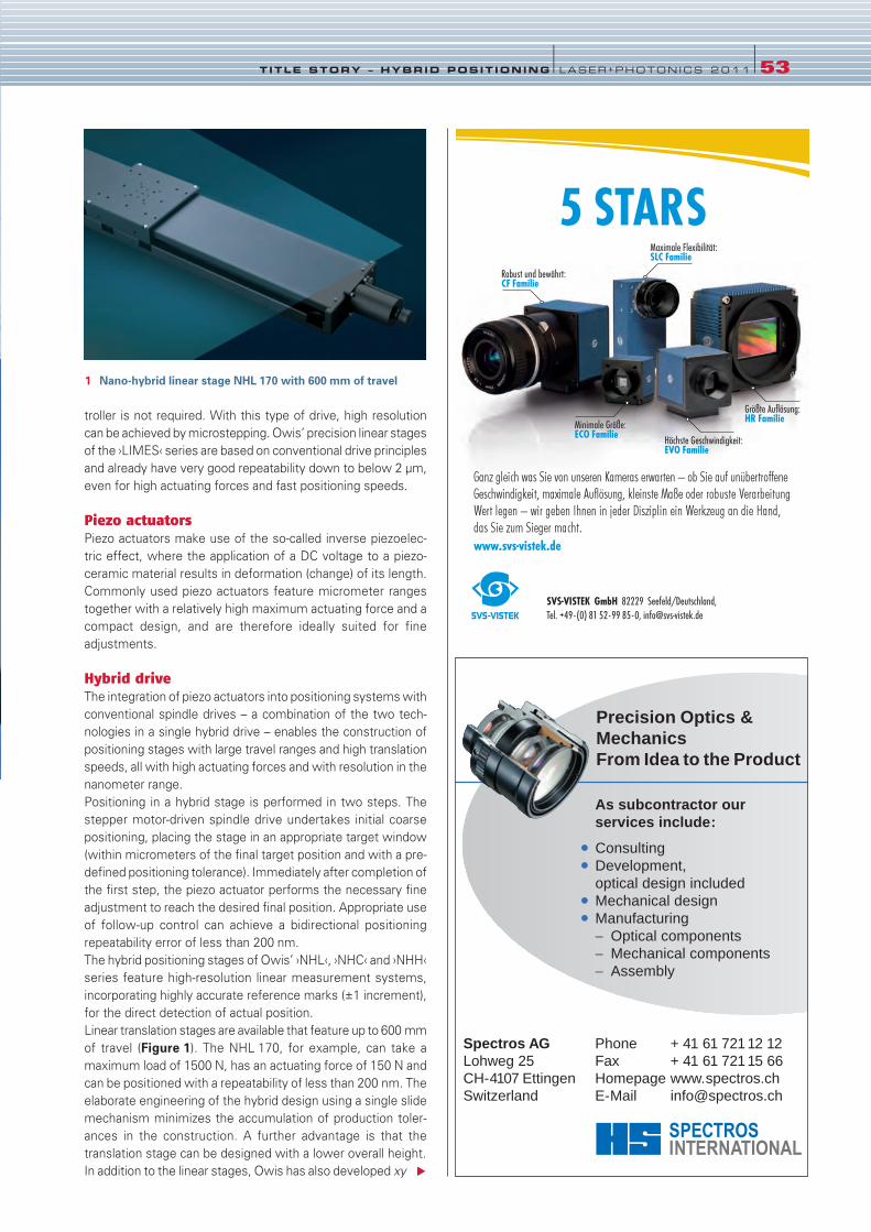
troller is not required. With this type of drive, high resolution
can be achieved by microstepping. Owis’ precision linear stages
of the ›LIMES‹ series are based on conventional drive principles
and already have very good repeatability down to below 2 µm,
even for high actuating forces and fast positioning speeds.
Piezo actuators
Piezo actuators make use of the so-called inverse piezoelec-
tric effect, where the application of a DC voltage to a piezo-
ceramic material results in deformation (change) of its length.
Commonly used piezo actuators feature micrometer ranges
together with a relatively high maximum actuating force and a
compact design, and are therefore ideally suited for fine
adjustments.
Hybrid drive
The integration of piezo actuators into positioning systems with
conventional spindle drives – a combination of the two tech-
nologies in a single hybrid drive – enables the construction of
positioning stages with large travel ranges and high translation
speeds, all with high actuating forces and with resolution in the
nanometer range.
Positioning in a hybrid stage is performed in two steps. The
stepper motor-driven spindle drive undertakes initial coarse
positioning, placing the stage in an appropriate target window
(within micrometers of the final target position and with a pre-
defined positioning tolerance). Immediately after completion of
the first step, the piezo actuator performs the necessary fine
adjustment to reach the desired final position. Appropriate use
of follow-up control can achieve a bidirectional positioning
repeatability error of less than 200 nm.
The hybrid positioning stages of Owis’ ›NHL‹, ›NHC‹ and ›NHH‹
series feature high-resolution linear measurement systems,
incorporating highly accurate reference marks (±1 increment),
for the direct detection of actual position.
Linear translation stages are available that feature up to 600 mm
of travel (Figure 1). The NHL 170, for example, can take a
maximum load of 1500 N, has an actuating force of 150 N and
can be positioned with a repeatability of less than 200 nm. The
elaborate engineering of the hybrid design using a single slide
mechanism minimizes the accumulation of production toler-
ances in the construction. A further advantage is that the
translation stage can be designed with a lower overall height.
In addition to the linear stages, Owis has also developed xy
T ITLE STORY – HYBRID POSIT IONING l LASER+PHOTONICS 2011 l53
1 Nano-hybrid linear stage NHL 170 with 600 mm of travel
Spectros AG Phone + 41 61 72112 12Lohweg 25 Fax + 41 61 72115 66CH-4107 Ettingen Homepage www.spectros.chSwitzerland E-Mail [email protected]
Precision Optics & MechanicsFrom Idea to the Product
As subcontractor our services include:
ConsultingDevelopment, optical design includedMechanical designManufacturing
Optical componentsMechanical componentsAssembly
Größte Auflösung: HR Familie
Robust und bewährt:CF Familie
Minimale Größe: ECO Familie
Maximale Flexibilität: SLC Familie
Höchste Geschwindigkeit:EVO Familie
SVS-VISTEK GmbH 82229 Seefeld/Deutschland, Tel. +49 - (0) 81 52 - 99 85 - 0, [email protected]
5 STARS
Ganz gleich was Sie von unseren Kameras erwarten – ob Sie auf unübertroffene Geschwindigkeit, maximale Auflösung, kleinste Maße oder robuste Verarbeitung Wert legen – wir geben Ihnen in jeder Disziplin ein Werkzeug an die Hand, das Sie zum Sieger macht.www.svs-vistek.de
V
52-54_LPX110087_LPX11 16.12.2010 18:29 Uhr Seite 53

and elevator stages as nano-hybrid versions. As with their
classical counterparts, the nano-hybrid NHC xy stages also
feature an aperture that remains largely free across the entire
travel range (Figure 2). Microscope positioning applications
requiring light transmission – and even involving loads of up to
15 kg – can now be realized with nanometer precision. For ap-
plications in which no aperture is required, this can be closed
with an appropriate insert.
Z-axis translation is provided by the NHH series elevator stages.
Versatile mounting options enable their flexible use – even
upside down. One example of this series is the NHH 200
(Figure 3) with its large actuating force of 200 N. This type of
stage is especially useful whenever free space is required above
the level of the mounting surface.
The physical dimensions of all of the newly developed hybrid
linear, xy and elevator stages are all identical to their conven-
tionally driven counterparts. Conventional stages can thus be
conveniently swapped out for high-resolution hybrid stages if
more precise positioning is required. Despite all the advantages,
Owis’ hybrid positioning technology is available at a very
attractive price/performance ratio.
Positioning control
All nano-hybrid positioners can be moved and controlled with
the ›PS 90‹ positioning control unit. The PS 90 allows standard
control modules for conventional stepper or DC servomotors
to be used in parallel with those for the new hybrid positioning
stages. For example, structures incorporating three translation
axes, whereby only one or two axes need to be positioned with
high precision, can be managed with just a single controller and
the appropriate software. For customers who already own a
PS 90, they can have this modified by Owis for use with the
new nano-hybrid modules.
The PS 90 also provides different operating modes for posi-
tioning with hybrid drives. The user can select, for example,
whether the control process is terminated automatically after
reaching the target position, or maintained actively in order to
compensate for drift in position caused, for example, by tem-
perature fluctuations.
The PS 90 even automatically identifies which of the two in-
terconnected positioning loops needs to be activated, that is,
which motor needs to be addressed. No additional switching
or use of two different types of equipment is required here,
thus making operation easier for the user.
Summary
With the 600 mm of travel provided by the NHL 170, Owis
offers the longest travel range for any nano-hybrid linear
positioning stage available on the market. Furthermore, com-
pact stages for applications in all three dimensions are feasible
via the nano-hybrid xy stages of the NHC series and the
nano-hybrid NHH 200 elevator stage. Even when all stages are
capable of carrying heavy loads and feature large travel ranges,
bidirectional repeatability is still always less than 200 nm. ■
54 l LASER+PHOTONICS 2 0 11 lT ITLE STORY – HYBRID POSIT IONING
3 Compact z-adjustment with the NHH 200 elevator stage2 Nano-hybrid xy stage NHC 50 with 50x50 mm2 aperture
OpTaliX Optical Design - Thin Films - IlluminationComprehensive Software for Optical Engineering
Optenso, Optical Engineering SoftwareKugelstr. 205, CH-9435 Heerbruggwww.optenso.com, [email protected]
Advanced optimization algorithms
Sequential and non-sequential surfaces Beam propagation and fiber couplingPolarization raytraceUser-defined surfaces and gradientsZoom and multiconfigurationEnvironmental analysisMacro language500+ examples, 8000+ catalogue lenses
Comprehensive Thin-Film PackageIllumination with real sources
52-54_LPX110087_LPX11 15.12.2010 18:05 Uhr Seite 54
Swiss, but at home all over the world.At WZW we have been producing high-end op-
tics and precision optical components for cus-
tomers all over the world for more than 40
years. Based in Balgach, Switzerland, our in-
novative company is a market leader in the en-
gineering and manufacture of high-end optics
and opto-mechanical assemblies. Our aim is to
strengthen our position even further, so it is vi-
tal that we act as a full-service provider to our
customers. We place the most rigorous de-
mands on our employees in everyway, from
product design, product development, quality
assurance procedures to prototyping and se-
ries production. This ensures first-rate prod-
ucts, and to help us sustain this level of quali-
ty we draw on our highly qualified staff and cut-
ting-edge technology. In 2009 WZWOPTICAG
invested in wafer dicing technology to dice
prism bars. This has created many opportuni-
ties within the medical industry, where the re-
quirement is for very small prisms with sharp
edges and no edge chips. The Tilting Spindle
capability is designed to provide both perpen-
dicular cuts and 8° angular cuts needed to sup-
press back-reflection in optic components.
Capabilities for High – End OpticsTECHNOLOGY• MRF – Magnetorheological Finishing
Flatness Lambda 60Angle correction < 0.1” arc sec
• Wafer dicing with tilting spindle capability
• Sub Angstrom Polishing < 1 Angström• Linked QS – system (ISO 9001:2008) since
1998
• 150m2 optical and opto-mechanical assem-
bly clean rooms
CAPABILITIES• Surface roughness < 1 Angström• Sizes of substrates 0.3–450 mm• Angle tolerances ± 0.4” arc seconds• Thickness Tolerance ± 0.0002mm
METROLOGYZygo New View 6300 (Å)
• Chapman MP2000 Plus Non-Contact Sur-
face Profiling System
• Autocollimator (resolution ± 1”)
• Interferometer ( Zygo, Fisba, Kugler)
PRODUCTS• Complexed cemented sub assemblies
• Development of OEM opto-mechanical and
electronic assemblies
• UV optics
• In and ex cavity optics
• Laser crystals
• Plano Optics
• Collimation systems
• Optical windows
• Free form in house production
Blanks within 48 hours
1mm 150mm (larger sizes on request)
Holes > 0.18mm
SERVICES• R&D Services
• Optical design (Oslo, Zemax)
• Mechanical design (3D CAD- solid edge)
• Spectrometry MTF measurement equip-
ment
• Environmental testing in house (–40º up to
180º)
Our diversity and unity brings creativity to our
relationships within our company, and to our
customers. We are also fortunate to be based
in one of the most beautiful regions, the Rhine
Valley in Switzerland. Our new Balgach facili-
ty covers 3,000 square meters and offers ex-
cellent working conditions including a clean
room environment and the latest technical
equipment, we even have enough space for
an in-house kindergarten.
WZWOPTICAGWegenstr. 18
9436 Balgach
Switzerland
Phone +41 (0)71 722-1214
Fax +41 (0)71 722-1240
www.wzw.ch
COMPANY PROF ILE l55
FirmenPortr_LPex2011 16.12.2010 18:30 Uhr Seite 55
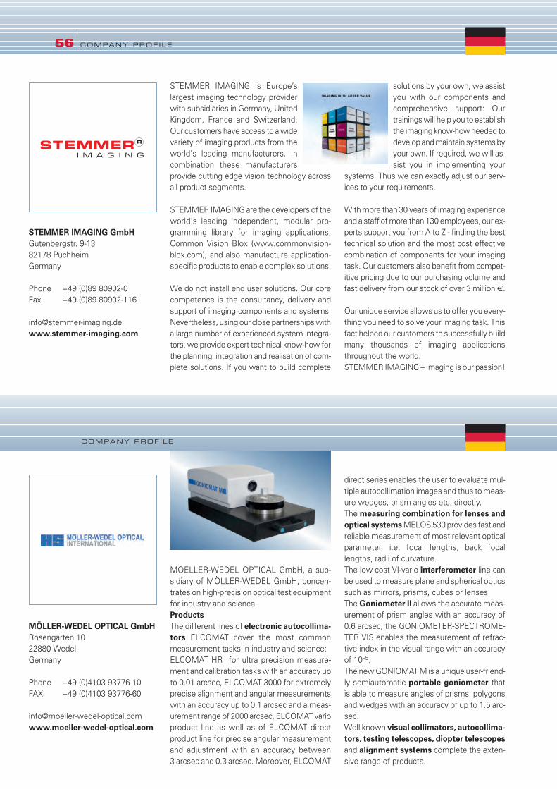
56 lCOMPANY PROF ILE
COMPANY PROF ILE
STEMMER IMAGING GmbHGutenbergstr. 9-13
82178 Puchheim
Germany
Phone +49 (0)89 80902-0
Fax +49 (0)89 80902-116
www.stemmer-imaging.com
STEMMER IMAGING is Europe’s
largest imaging technology provider
with subsidiaries in Germany, United
Kingdom, France and Switzerland.
Our customers have access to a wide
variety of imaging products from the
world's leading manufacturers. In
combination these manufacturers
provide cutting edge vision technology across
all product segments.
STEMMER IMAGING are the developers of the
world's leading independent, modular pro-
gramming library for imaging applications,
Common Vision Blox (www.commonvision-
blox.com), and also manufacture application-
specific products to enable complex solutions.
We do not install end user solutions. Our core
competence is the consultancy, delivery and
support of imaging components and systems.
Nevertheless, using our close partnerships with
a large number of experienced system integra-
tors, we provide expert technical know-how for
the planning, integration and realisation of com-
plete solutions. If you want to build complete
solutions by your own, we assist
you with our components and
comprehensive support: Our
trainings will help you to establish
the imaging know-how needed to
develop and maintain systems by
your own. If required, we will as-
sist you in implementing your
systems. Thus we can exactly adjust our serv-
ices to your requirements.
With more than 30 years of imaging experience
and a staff of more than 130 employees, our ex-
perts support you from A to Z - finding the best
technical solution and the most cost effective
combination of components for your imaging
task. Our customers also benefit from compet-
itive pricing due to our purchasing volume and
fast delivery from our stock of over 3 million €.
Our unique service allows us to offer you every-
thing you need to solve your imaging task. This
fact helped our customers to successfully build
many thousands of imaging applications
throughout the world.
STEMMER IMAGING – Imaging is our passion!
MÖLLER-WEDEL OPTICAL GmbHRosengarten 10
22880 Wedel
Germany
Phone +49 (0)4103 93776-10
FAX +49 (0)4103 93776-60
www.moeller-wedel-optical.com
MOELLER-WEDEL OPTICAL GmbH, a sub-
sidiary of MÖLLER-WEDEL GmbH, concen-
trates on high-precision optical test equipment
for industry and science.
ProductsThe different lines of electronic autocollima-tors ELCOMAT cover the most common
measurement tasks in industry and science:
ELCOMAT HR for ultra precision measure-
ment and calibration tasks with an accuracy up
to 0.01 arcsec, ELCOMAT 3000 for extremely
precise alignment and angular measurements
with an accuracy up to 0.1 arcsec and a meas-
urement range of 2000 arcsec, ELCOMAT vario
product line as well as of ELCOMAT direct
product line for precise angular measurement
and adjustment with an accuracy between
3 arcsec and 0.3 arcsec. Moreover, ELCOMAT
direct series enables the user to evaluate mul-
tiple autocollimation images and thus to meas-
ure wedges, prism angles etc. directly.
The measuring combination for lenses andoptical systems MELOS 530 provides fast and
reliable measurement of most relevant optical
parameter, i.e. focal lengths, back focal
lengths, radii of curvature.
The low cost VI-vario interferometer line can
be used to measure plane and spherical optics
such as mirrors, prisms, cubes or lenses.
The Goniometer II allows the accurate meas-
urement of prism angles with an accuracy of
0.6 arcsec, the GONIOMETER-SPECTROME-
TER VIS enables the measurement of refrac-
tive index in the visual range with an accuracy
of 10–5.
The new GONIOMAT M is a unique user-friend-
ly semiautomatic portable goniometer that
is able to measure angles of prisms, polygons
and wedges with an accuracy of up to 1.5 arc-
sec.
Well known visual collimators, autocollima-tors, testing telescopes, diopter telescopesand alignment systems complete the exten-
sive range of products.
FirmenPortr_LPex2011 15.12.2010 12:28 Uhr Seite 56
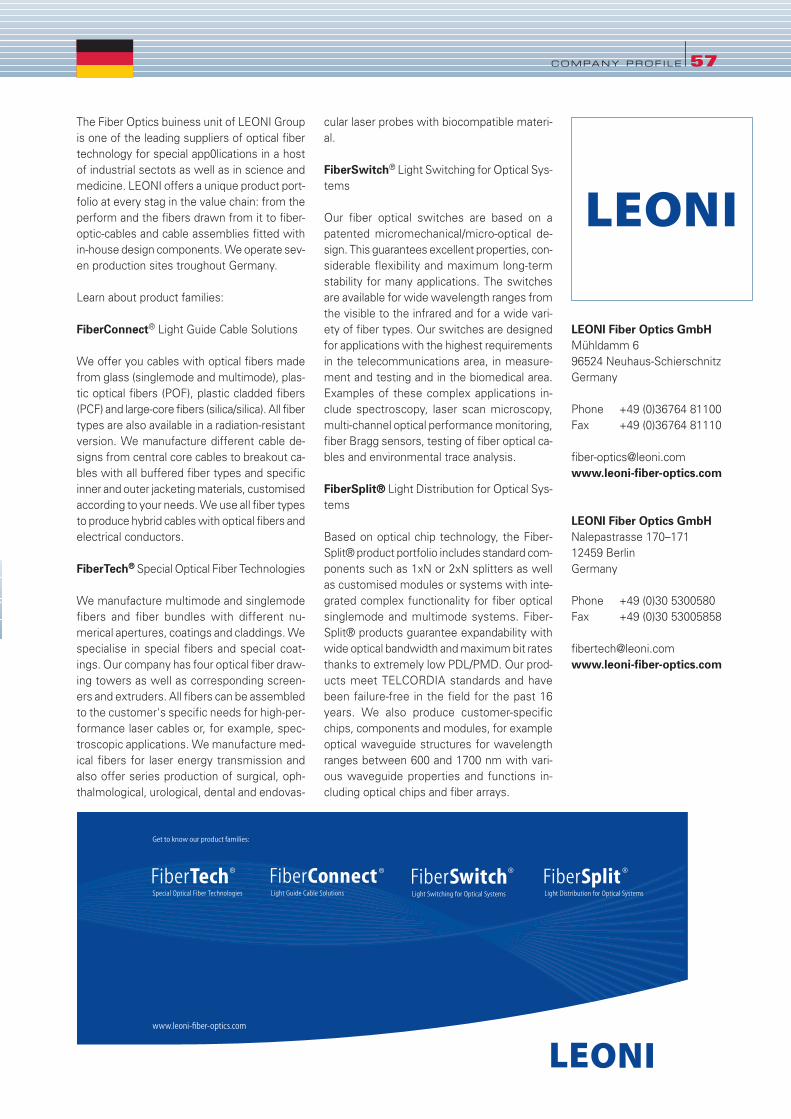
COMPANY PROF ILE l57
www.leoni-fi ber-optics.com
:
The Fiber Optics buiness unit of LEONI Group
is one of the leading suppliers of optical fiber
technology for special app0lications in a host
of industrial sectots as well as in science and
medicine. LEONI offers a unique product port-
folio at every stag in the value chain: from the
perform and the fibers drawn from it to fiber-
optic-cables and cable assemblies fitted with
in-house design components. We operate sev-
en production sites troughout Germany.
Learn about product families:
FiberConnect® Light Guide Cable Solutions
We offer you cables with optical fibers made
from glass (singlemode and multimode), plas-
tic optical fibers (POF), plastic cladded fibers
(PCF) and large-core fibers (silica/silica). All fiber
types are also available in a radiation-resistant
version. We manufacture different cable de-
signs from central core cables to breakout ca-
bles with all buffered fiber types and specific
inner and outer jacketing materials, customised
according to your needs. We use all fiber types
to produce hybrid cables with optical fibers and
electrical conductors.
FiberTech® Special Optical Fiber Technologies
We manufacture multimode and singlemode
fibers and fiber bundles with different nu-
merical apertures, coatings and claddings. We
specialise in special fibers and special coat-
ings. Our company has four optical fiber draw-
ing towers as well as corresponding screen-
ers and extruders. All fibers can be assembled
to the customer's specific needs for high-per-
formance laser cables or, for example, spec-
troscopic applications. We manufacture med-
ical fibers for laser energy transmission and
also offer series production of surgical, oph-
thalmological, urological, dental and endovas-
cular laser probes with biocompatible materi-
al.
FiberSwitch® Light Switching for Optical Sys-
tems
Our fiber optical switches are based on a
patented micromechanical/micro-optical de-
sign. This guarantees excellent properties, con-
siderable flexibility and maximum long-term
stability for many applications. The switches
are available for wide wavelength ranges from
the visible to the infrared and for a wide vari-
ety of fiber types. Our switches are designed
for applications with the highest requirements
in the telecommunications area, in measure-
ment and testing and in the biomedical area.
Examples of these complex applications in-
clude spectroscopy, laser scan microscopy,
multi-channel optical performance monitoring,
fiber Bragg sensors, testing of fiber optical ca-
bles and environmental trace analysis.
FiberSplit® Light Distribution for Optical Sys-
tems
Based on optical chip technology, the Fiber-
Split® product portfolio includes standard com-
ponents such as 1xN or 2xN splitters as well
as customised modules or systems with inte-
grated complex functionality for fiber optical
singlemode and multimode systems. Fiber-
Split® products guarantee expandability with
wide optical bandwidth and maximum bit rates
thanks to extremely low PDL/PMD. Our prod-
ucts meet TELCORDIA standards and have
been failure-free in the field for the past 16
years. We also produce customer-specific
chips, components and modules, for example
optical waveguide structures for wavelength
ranges between 600 and 1700 nm with vari-
ous waveguide properties and functions in-
cluding optical chips and fiber arrays.
LEONI Fiber Optics GmbHMühldamm 6
96524 Neuhaus-Schierschnitz
Germany
Phone +49 (0)36764 81100
Fax +49 (0)36764 81110
www.leoni-fiber-optics.com
LEONI Fiber Optics GmbHNalepastrasse 170–171
12459 Berlin
Germany
Phone +49 (0)30 5300580
Fax +49 (0)30 53005858
www.leoni-fiber-optics.com
FirmenPortr_LPex2011 15.12.2010 12:28 Uhr Seite 57
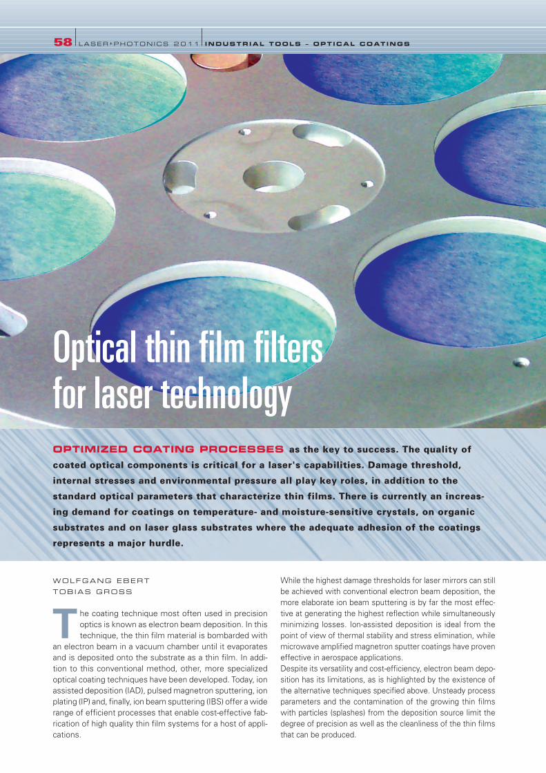
WOLFGANG EBERT
TOBIAS GROSS
T he coating technique most often used in precision
optics is known as electron beam deposition. In this
technique, the thin film material is bombarded with
an electron beam in a vacuum chamber until it evaporates
and is deposited onto the substrate as a thin film. In addi-
tion to this conventional method, other, more specialized
optical coating techniques have been developed. Today, ion
assisted deposition (IAD), pulsed magnetron sputtering, ion
plating (IP) and, finally, ion beam sputtering (IBS) offer a wide
range of efficient processes that enable cost-effective fab-
rication of high quality thin film systems for a host of appli-
cations.
While the highest damage thresholds for laser mirrors can still
be achieved with conventional electron beam deposition, the
more elaborate ion beam sputtering is by far the most effec-
tive at generating the highest reflection while simultaneously
minimizing losses. Ion-assisted deposition is ideal from the
point of view of thermal stability and stress elimination, while
microwave amplified magnetron sputter coatings have proven
effective in aerospace applications.
Despite its versatility and cost-efficiency, electron beam depo-
sition has its limitations, as is highlighted by the existence of
the alternative techniques specified above. Unsteady process
parameters and the contamination of the growing thin films
with particles (splashes) from the deposition source limit the
degree of precision as well as the cleanliness of the thin films
that can be produced.
58 l LASER+PHOTONICS 2 0 11 l INDUSTRIAL TOOLS – OPT ICAL COATINGS
Optical thin film filters for laser technology OPTIMIZED COATING PROCESSES as the key to success. The quality of
coated optical components is critical for a laser's capabilities. Damage threshold,
internal stresses and environmental pressure all play key roles, in addition to the
standard optical parameters that characterize thin films. There is currently an increas-
ing demand for coatings on temperature- and moisture-sensitive crystals, on organic
substrates and on laser glass substrates where the adequate adhesion of the coatings
represents a major hurdle.
58-61_LPX110049_LPX11 15.12.2010 18:08 Uhr Seite 58

A further restriction is posed by the relatively low kinetic ener-
gy of the adatoms (<1 eV). The films typically have a reduced
packing density and exhibit pores and, in some cases, column
formation (Figure 1). The voids between the columns, which
may account for up to 30 percent of the volume, fill with water
when exposed to humid air. Some of
this water is expelled through evacua-
tion or – for example, when using laser
power – are heated. The subsequent
desorption of the water causes the
spectral properties to shift to shorter
wavelengths. For example, the trans-
mission profile of a typical mirror shifts
by approximately one to two percent
on the wavelength scale when the tem-
perature is increased from 20 to 120°C
(Figure 2). Conventional deposition is
therefore unsuitable for certain com-
plex applications. Higher energy tech-
niques minimize this effect, while for
IBS it is barely perceptible (Figure 3and 4).
(Almost) perfect
laser mirrors with IBS
The IBS technique originated in a patent
dating from 1978 [1]. This patent de-
scribes a method of fabricating high
quality mirrors for laser gyroscopes
that minimizes losses due to light scat-
ter. An ion beam source directs inert
gas ions onto a plate of the coating
material, referred to as the target. Due
to the high kinetic energy of the inert
gas ions (typically 1250 eV), a cascade
of collisions causes atoms to be sput-
tered or ejected out of the target.
These then condense onto the sub-
strate that is to be coated. As the mean
kinetic energy of these adatoms is in
the region of several eV, and therefore
higher by one or two orders of magni-
tude than in thermal deposition, the
thin films that are fabricated are ab-
solutely compact, have an amorphous
microstructure and a low roughness
value (Figure 5).
Thanks to the application of industrial technology, ion beam
sputtering evolved into an established technique and took a
huge leap forward in terms of development. A key factor in this
development was the replacement of the high maintenance
Kaufman sources (based on hot cathodes) with high frequen-
cy ion sources with long-term stability. The latter had original-
ly been developed as a means of propulsion for aerospace
applications at the University of Giessen [2].
Industrial IBS systems today are equipped with a second ion
source directed at the substrate, which can, if required, be used
to pre-treat the substrate (cleaning/etching) prior to coating, or
to assist with coating (Figure 6). Current coating rates are in
INDUSTRIAL TOOLS – OPT ICAL COATINGS l LASER+PHOTONICS 2011 l59
1 One of the first images of a fracture edge of TiO2 and SiO2
captured on an electron microscope by K.-H. Günther in the early 1980s. The porous column structure is clearly visible.The column structure of the titanium dioxide has even been carried over to the otherwise smooth silicon dioxide
2 The filter curve of a mirror coated with electron beam deposition is highly temperature-sensitive because of the porous nature of the microstructure. The spectral shift can be explained by water ab- and desorption and the associated changes in refractive index
© LASER+PHOTONICS
3 The transmission curve of an IBS filter is temperature-stable
© LASER+PHOTONICS
V
Wavelength [nm]
Wavelength [nm]
58-61_LPX110049_LPX11 15.12.2010 18:08 Uhr Seite 59

the region of 0.25 nm/s (depending on the material), with sub-
strates occupying areas up to approximately 500 cm2.
The technique is clearly inferior to other methods in terms of
productivity, but is nevertheless often the only workable solu-
tion for certain applications. For example, so-called super mirrors
need to show light scatter losses of significantly less than
10 ppm at 633 nm in the laser gyroscope application mentioned
above, specifications that are achievable with IBS. Indeed, light
scatter loss measurements (TBS, total backscattering in accor-
dance with ISO13696) undertaken by the Fraunhofer Institute
for Applied Optics and Precision Mechanics in Jena on a mirror
manufactured by Laseroptik was found to exhibit a TBS of just
1.1 ppm. With typical absorption and residual transmission
measuring <15 ppm in total, the resulting reflectivity of
>99.998 percent comes very close to that of a perfect mirror
[3]. This type of result can, however, only be achieved with super
polished substrates (surface roughness <1 Å rms) and provid-
ed that all rules relating to cleanroom procedures and clean-
liness are scrupulously observed.
Another key application for super mirrors is in cavity ring-down
measurements. Cavity ring-down spectroscopy [4] measures
the ring-down time of a resonator and so too the resonator
losses, thus revealing trace gas concentrations in the resonator.
Alongside IBS, CRD is used as a measuring method in quality
assurance to determine the losses of such highly reflective
optics. As a result, measurements of more than six nines
(99.9999 percent) are achievable, provided that the reference
optics in the measuring instrument are adequate.
IBS for precise high performance coatings
In contrast to conventional electron beam deposition, IBS coat-
ings have no column structure, no voids or splashes and demon-
strate no contamination due to poor vacuum conditions, all of
which could lead to absorption or scatter. In addition, the sta-
bility of the optical constants is excellent. For most coating
prozesses, and as is standard in all sputtering processes, thin
film growth can be determined based
on time interval measurement using
the vibrating quartz method.
However, for broadband, chirped mir-
rors for fs pulse generation, very steep-
edged filters, non-polarizing beam split-
ters or bandpass filters, then thin film
thickness needs to be monitored via its
broadband optical transmission. This
technique measures the transmission
curve in situ at the corresponding tar-
get spot on the rotating substrate with-
in the coating system. Comparison of
the actual transmission spectrum with
that expected for the current layer stack
reveals the thickness of the top layer,
and this information is used to control
the continuing process appropriately.
Minimizing the unexpected in this fash-
ion yields a high level of process relia-
bility and simultaneously reduces the
risk regarding cost-intensive substrates
such as for nonlinear or laser crystals,
fiber end-facets, semiconductors or the
super polished optics mentioned above.
The fabrication of phase-optimized mirrors represents another
field of application that justifies the use of the IBS approach in
conjunction with sophisticated processes control. So-called
chirped mirrors are used in
femtosecond lasers to
negate the normal dispersive
effects of other laser com-
ponents. For example, a mir-
ror can be modified to
stretch fs pulses before the
amplification stage, while a
complementary mirror re-
compresses them again following the amplification stage, thus
protecting the components within from excessive intensity.
New directions are also being explored with novel approaches
such as the sputtering of fluoride materials or the fabrication of
rugate filters. Instead of a sequence of thin films with alternat-
60 l LASER+PHOTONICS 2 0 11 l INDUSTRIAL TOOLS – OPT ICAL COATINGS
4 A comparison between the thermally induced spectral shift for the IBS filter fromFigure 3 and the thin film system from Figure 2. Other, considerably more minoreffects dominate in the absence of the negative shift caused by thin film pores (thetemperature sensitivity of the refractive indexes and the thermal expansion of thethin film and substrate materials)
© LASER+PHOTONICS
5 Electron microscope image of an Nb2O5/SiO2 composite film fabricated using IBS. The films are free of voids and have a perfectly amorphous microstructure and extremelysmooth surfaces
LASEROPTIK GmbH 30826 Garbsen, Germany
Tel. +49 (0)5131 4597-0
Fax +49 (0)5131 4597-20
www.laseroptik.de
CONTACT
Temperature [°C]
rel.
spec
tral
shi
ft
surface
58-61_LPX110049_LPX11 15.12.2010 18:08 Uhr Seite 60
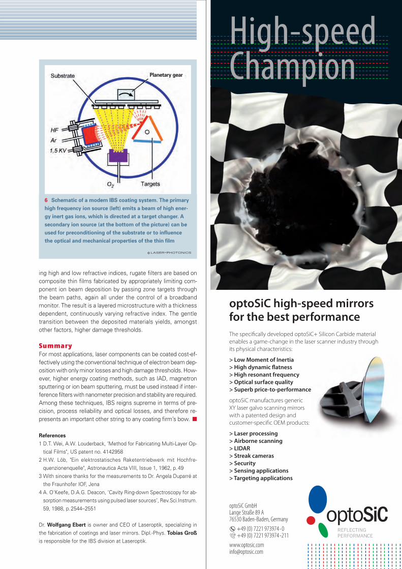
ing high and low refractive indices, rugate filters are based on
composite thin films fabricated by appropriately limiting com-
ponent ion beam deposition by passing zone targets through
the beam paths, again all under the control of a broadband
monitor. The result is a layered microstructure with a thickness
dependent, continuously varying refractive index. The gentle
transition between the deposited materials yields, amongst
other factors, higher damage thresholds.
Summary
For most applications, laser components can be coated cost-ef-
fectively using the conventional technique of electron beam dep-
osition with only minor losses and high damage thresholds. How-
ever, higher energy coating methods, such as IAD, magnetron
sputtering or ion beam sputtering, must be used instead if inter-
ference filters with nanometer precision and stability are required.
Among these techniques, IBS reigns supreme in terms of pre-
cision, process reliability and optical losses, and therefore re-
presents an important other string to any coating firm’s bow. ■
References 1 D.T. Wei, A.W. Louderback, ‘Method for Fabricating Multi-Layer Op-
tical Films", US patent no. 4142958
2 H.W. Löb, "Ein elektrostatisches Raketentriebwerk mit Hochfre-
quenzionenquelle", Astronautica Acta VIII, Issue 1, 1962, p.49
3 With sincere thanks for the measurements to Dr. Angela Duparré at
the Fraunhofer IOF, Jena
4 A. O'Keefe, D.A.G. Deacon, ‘Cavity Ring-down Spectroscopy for ab-
sorption measurements using pulsed laser sources’, Rev.Sci.Instrum.
59, 1988, p.2544–2551
Dr. Wolfgang Ebert is owner and CEO of Laseroptik, specializing in
the fabrication of coatings and laser mirrors. Dipl.-Phys. Tobias Großis responsible for the IBS division at Laseroptik.
6 Schematic of a modem IBS coating system. The primaryhigh frequency ion source (left) emits a beam of high ener-gy inert gas ions, which is directed at a target changer. Asecondary ion source (at the bottom of the picture) can beused for preconditioning of the substrate or to influencethe optical and mechanical properties of the thin film
© LASER+PHOTONICS
High-speed Champion
optoSiC GmbHLange Straße 89 A76530 Baden-Baden, Germany
2 +49 (0) 7221 973974-05 +49 (0) 7221 973974 -211www.optosic.com [email protected]
optoSiC high-speed mirrors for the best performanceThe specifically developed optoSiC+ Silicon Carbide material enables a game-change in the laser scanner industry through its physical characteristics:
> Low Moment of Inertia> High dynamic flatness> High resonant frequency> Optical surface quality> Superb price-to-performance
optoSiC manufactures generic XY laser galvo scanning mirrors with a patented design and customer-specific OEM products:
> Laser processing> Airborne scanning> LIDAR> Streak cameras> Security> Sensing applications> Targeting applications
Planetary gear
58-61_LPX110049_LPX11 16.12.2010 18:32 Uhr Seite 61

R ICHARD HENDEL
To cope with the intense competition in the solar
market, costs need to be reduced. However, manu-
facturers of crystalline cells have very little scope
when it comes to reducing costs. Their current focus is on
saving material by reducing wafer thickness or the silver
pastes used, cutting production losses and further improv-
ing system availability. What all of these have in common,
however, is that the potential cost savings are relatively small.
As a result, attention is being increasingly given to a second
variable for optimizing the price per watt – optimizing efficien-
cy. The performance of research-grade crystalline cells with up
to two thirds better efficiency demonstrate what is techno-
logically feasible, although, of course, any increase in efficien-
cy at the market level needs to be achieved with the lowest
possible additional investment costs.
Cell manufacturers and suppliers of photovoltaic production
lines alike are now faced with the task of identifying opti-
mization technologies that require few additional process steps
and that can be integrated into existing production line in-
stallations. Material processing using lasers is a very popular
process here. It allows optimum control and, compared to etch-
ing and diffusion methods, runs at lower cost and with fewer
materials, allowing it to be integrated into production process-
es with comparative ease.
Selective emitter technology
The most promising solution at present is actually ancient by
photovoltaics standards. It is based around selective emitters,
which were already being discussed back in the 1970’s. This
technology promises to deliver an efficiency increase of up to
one percentage point (to around 17 percent for multi-crystalline
and 18.5 percent for mono-crystalline cells).
Traditional crystalline solar cells essentially consist of a full-
metalized rear, a thick, p-doped silicon layer, a passivation and
anti-reflection layer, and the fine metallic contact grid on the
front. In the past, a compromise always had to be found for the
negative phosphorous-doping of the silicon layer. While high
doping around the contact fingers is desirable for effective
conduction and low transition resistances, this reduces the
efficiency in the areas in between due to unwanted absorption
and recombination effects. In particular, this results in an effi-
ciency loss of up to a third for solar cells in the short-wave
near-UV spectral range.
Selective emitters for mass production
The solution has actually been on hand for a long time – selec-
tive doping of the emitter layer (Figure 1). However, in the past,
the process was seen as too complex for mass production. This
is because a second, separate doping step to achieve the
different doping levels complicates the production process, as
it actually involves several complex steps (marking, diffusion,
etching). In addition, precise alignment of the higher doped
areas with the contact fingers (attached later) calls for an
extremely accurate process technology.
62 l LASER+PHOTONICS 2 0 11 lMATERIALS PROCESSING – PV
Selective doping LASER TECHNOLOGY HELPSSOLAR CELLS with selective emitters
to enter mass production. Within a year,
the photovoltaics market has seen a price
fall of 30 to 50 percent. The forthcoming
new regulations to reduce energy feed-in
tariffs (FITs) will exert further pressure on
prices. To cope with the intensified com-
petition, costs have to be reduced – one
way to do that is to optimize efficiency. A dielectric layer with typical finger grid
1 Schematic diagram of the selective emitting region
62-64_LPX110010_LPX11 15.12.2010 18:15 Uhr Seite 62

These days there are several new process
concepts that avoid these disad-
vantages. All of the major German
integrators and system suppliers –
Roth & Rau, Manz, Schmid and Cen-
trotherm – are working intensively on
this problem. China Sunenergy has become
the first major manufacturer to integrate se-
lective emitters into its volume production.
Apart from the ›etch-back‹ technology, which
first creates broad-area highly-doped emitters
and then selectively weakens the same layer
by etching, they all use laser technology in one
or more process steps.
Laser ablation to achieve selective
doping processes
The ›diffusion masking‹ method is currently at a very advanced
stage of development. It involves masking the wafers with a
dielectric layer before phosphorous diffusion, and selectively
opening this mask with the laser in the areas where the
contacts will subsequently be located. This enables the sub-
sequent standard diffusion process used for doping to act at
different strengths on the different areas of the surface.
After comparing numerous processes available, one manufac-
turer of production systems chose this technology and pre-
sented it at the 24th European Photovoltaic Solar Energy
Conference in September 2009. In the process outlined, the
laser ablates the dielectric layer at a
width that is slightly above the con-
tact path that will subsequently be print-
ed. The laser process is designed to be as
fast and effective as possible and, at the
same time, optimized to ensure the least
possible damage to the underlying silicon.
Direct selective laser doping
Direct, selective laser doping is another
interesting method for producing selective
emitters. With its accurate, precisely controllable
local heat injection, a laser is the best way to meet the
requirements for a selective doping process. Earlier concepts
used the laser for doping with gaseous or liquid doping sources,
combined with correspondingly sophisticated process tech-
nology. By contrast, new technologies are mainly based on ›dry‹
methods with local ›driving-in‹ of solid doping materials previ-
ously applied.
The simplest method,
which was first discussed
back in the 1990’s, uses
the layer of phosphosili-
cate glass (PSG) (that is,
the layer that is found on
the surface after conven-
tional doping) as a doping
source for a second, se-
lective doping step (Fig-ure 2). A laser locally heats or melts the silicon surface below
the PSG layer, thus allowing deeper penetration of additional
phosphorous doping. However, the task of subsequently align-
ing the heavily doped emitter with the contact grid remains.
Other concepts move this step backwards in the process, and
apply a phosphorous doping source to the passivation layer
immediately before producing the upper contacts. A laser beam
ablates the dielectric layer and melts the silicon underneath in
a fine lattice, thus allowing the additional doping to penetrate.
The metalization for the contact fingers can then be immedi-
ately applied to the open, highly-doped emitter layers.
MATERIALS PROCESSING – PV l LASER+PHOTONICS 2011 l63
2 PSG doping in a scanning electron microscope image
ROFIN Baasel Lasertech GmbH & Co. KG82319 Starnberg, Germany
Tel. +49 (0)8151 776-0
Fax +49 (0)8151 776-4159
www.rofin.com
CONTACT
GMP-Normwww.spetec.de
Cleanroom Class ISO 5
6 different sizes
Width 60 to 183 cm
Laminar Flowbox
Cleanroom Class ISO 5
Modular
Flexible
Up to 25 m2
Please ask us for further information or send us an e-mail:
� +49-8122/99533Fax: +49-8122/10397E-Mail: [email protected]
SPETEC® GmbHPostfach 1517, D-85425 Erding
Cleanroom TechnologyCleanroom Cell
3 PowerLine L with fiber and scanning head
V
62-64_LPX110010_LPX11 17.12.2010 9:01 Uhr Seite 63

Green solid state lasers and
innovative fibers
The requisite beam quality at high powers and pulse frequen-
cies make Q-switched solid state lasers an ideal tool for this
kind of application. They are often used with frequency dou-
bling to provide optimum interaction with the thin film materi-
als used. The proper balance of pulse duration and energy
provides the most selective ablation possible. The short cycle
times available in mass production of solar cells necessitate
beam sources with output powers of up to 100 W, depending
on the application.
While the absorption at the fundamental wavelength of
1064 nm reaches too far into the deeper silicon layers, it can
be limited with frequency-doubled green lasers in the range of
1 µm. Frequency-tripled beam sources in the near UV range
demonstrate slightly better absorption properties in some
cases. However, this is offset by the relatively narrow choice
of UV-compatible optical components and the significantly more
critical maintenance issues, meaning they are not ideally suit-
ed for the requirements of industrial mass production.
Current projects by various research institutions and solar cell
manufacturers are confirming the exceptional suitability of
Rofin’s new ›PowerLine L 100 SHG‹ at 532 nm (Figure 3),
both for selective ablation of dielectric layers and for direct
laser doping. New optical fibers developed specifically for
this wavelength play a crucial role. They produce a ›top hat‹
beam profile, which represents the optimum solution for
homogeneous input of laser energy over the entire area of
the laser spot. This enables ablation and diffusion processes
with a much more uniform, two-dimensional intensity distri-
bution to be realized.
Summary
Photovoltaics remains a promising and yet demanding market
for laser manufacturers. Both new high efficiency concepts and
optimizations in mass production can only be achieved through
close cooperation with research institutions, system suppliers
and producers. With selective emitter technology, an old idea
has been successfully applied to research-grade solar cells and
is now starting to move into mass production. It will definitely
not be the last idea to do so. Lasers are also the key techno-
logy for a range of other high efficiency concepts that have
already been realized in practice, from ›laser fired contacts‹, to
›laser buried contacts‹ to ›back contact‹ cells.
In addition, the capability of lasers in terms of laser doping and
selective ablation of dielectric layers is opening up a wide range
of new methods for increasing efficiency. Because the layer
thicknesses for selective ablation are in the range from 10 to
several 100 nm, the requirements in terms of beam quality,
pulse to pulse stability and long-term stability of the lasers are
huge. This will call for the continued development of special
beam sources optimized for photovoltaics, such as the Rofin
PowerLine L series. ■
Richard Hendel is Sales Manager for Solar at Rofin Baasel Lasertech
in Starnberg. With 1600 employees, Rofin is one of the world’s lead-
ing manufacturers of industrial lasers and laser systems and has installed
well in excess of 1000 beam sources in the PV sector.
64 l LASER+PHOTONICS 2 0 11 lMATERIALS PROCESSING – PV
62-64_LPX110010_LPX11 15.12.2010 18:15 Uhr Seite 64
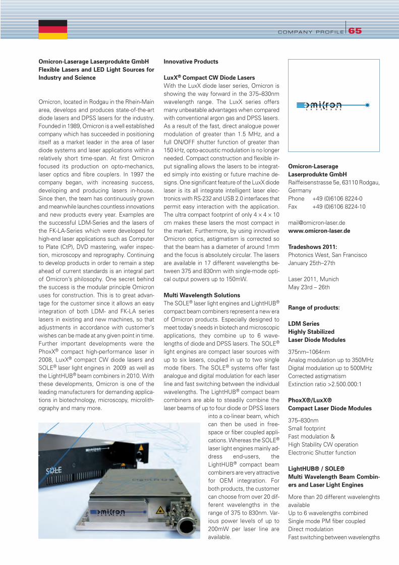
Omicron-Laserage Laserprodukte GmbHRaiffeisenstrasse 5e, 63110 Rodgau,
Germany
Phone +49 (0)6106 8224-0
Fax +49 (0)6106 8224-10
www.omicron-laser.de
Tradeshows 2011:Photonics West, San Francisco
January 25th–27th
Laser 2011, Munich
May 23rd – 26th
Range of products:
LDM Series Highly Stabilized Laser Diode Modules
375nm–1064nm
Analog modulation up to 350MHz
Digital modulation up to 500MHz
Corrected astigmatism
Extinction ratio >2.500.000:1
PhoxX®/LuxX® Compact Laser Diode Modules
375–830nm
Small footprint
Fast modulation &
High Stability CW operation
Electronic Shutter function
LightHUB® / SOLE®Multi Wavelength Beam Combin-ers and Laser Light Engines
More than 20 different wavelenghts
available
Up to 6 wavelengths combined
Single mode PM fiber coupled
Direct modulation
Fast switching between wavelengths
Omicron-Laserage Laserprodukte GmbHFlexible Lasers and LED Light Sources forIndustry and Science
Omicron, located in Rodgau in the Rhein-Main
area, develops and produces state-of-the-art
diode lasers and DPSS lasers for the industry.
Founded in 1989, Omicron is a well established
company which has succeeded in positioning
itself as a market leader in the area of laser
diode systems and laser applications within a
relatively short time-span. At first Omicron
focused its production on opto-mechanics,
laser optics and fibre couplers. In 1997 the
company began, with increasing success,
developing and producing lasers in-house.
Since then, the team has continuously grown
and meanwhile launches countless innovations
and new products every year. Examples are
the successful LDM-Series and the lasers of
the FK-LA-Series which were developed for
high-end laser applications such as Computer
to Plate (CtP), DVD mastering, wafer inspec-
tion, microscopy and reprography. Continuing
to develop products in order to remain a step
ahead of current standards is an integral part
of Omicron’s philosophy. One secret behind
the success is the modular principle Omicron
uses for construction. This is to great advan-
tage for the customer since it allows an easy
integration of both LDM- and FK-LA series
lasers in existing and new machines, so that
adjustments in accordance with customer’s
wishes can be made at any given point in time.
Further important developments were the
PhoxX® compact high-performance laser in
2008, LuxX® compact CW diode lasers and
SOLE® laser light engines in 2009 as well as
the LightHUB® beam combiners in 2010. With
these developments, Omicron is one of the
leading manufacturers for demanding applica-
tions in biotechnology, microscopy, microlith-
ography and many more.
Innovative Products
LuxX® Compact CW Diode LasersWith the LuxX diode laser series, Omicron is
showing the way forward in the 375–830nm
wavelength range. The LuxX series offers
many unbeatable advantages when compared
with conventional argon gas and DPSS lasers.
As a result of the fast, direct analogue power
modulation of greater than 1.5 MHz, and a
full ON/OFF shutter function of greater than
150 kHz, opto-acoustic modulation is no longer
needed. Compact construction and flexible in-
put signalling allows the lasers to be integrat-
ed simply into existing or future machine de-
signs. One significant feature of the LuxX diode
laser is its all integrate intelligent laser elec-
tronics with RS-232 and USB 2.0 interfaces that
permit easy interaction with the application.
The ultra compact footprint of only 4 × 4 × 10
cm makes these lasers the most compact in
the market. Furthermore, by using innovative
Omicron optics, astigmatism is corrected so
that the beam has a diameter of around 1mm
and the focus is absolutely circular. The lasers
are available in 17 different wavelengths be-
tween 375 and 830nm with single-mode opti-
cal output powers up to 150mW.
Multi Wavelength SolutionsThe SOLE® laser light engines and LightHUB®
compact beam combiners represent a new era
of Omicron products. Especially designed to
meet today´s needs in biotech and microscopic
applications, they combine up to 6 wave-
lengths of diode and DPSS lasers. The SOLE®
light engines are compact laser sources with
up to six lasers, coupled in up to two single
mode fibers. The SOLE® systems offer fast
analogue and digital modulation for each laser
line and fast switching between the individual
wavelengths. The LightHUB® compact beam
combiners are able to steadily combine the
laser beams of up to four diode or DPSS lasers
into a co-linear beam, which
can then be used in free-
space or fiber coupled appli-
cations. Whereas the SOLE®
laser light engines mainly ad-
dress end-users, the
LightHUB® compact beam
combiners are very attractive
for OEM integration. For
both products, the customer
can choose from over 20 dif-
ferent wavelengths in the
range of 375 to 830nm. Var-
ious power levels of up to
200mW per laser line are
available.
COMPANY PROF ILE l65
FirmenPortr_LPex2011 15.12.2010 12:29 Uhr Seite 65

66 lCOMPANY PROF ILE
COMPANY PROF ILE
RAYLASE AGArgelsrieder Feld 2+4
82234 Wessling
Germany
Phone +49 (0) 8153/88 98-0
Fax +49 (0) 8153/88 98-10
RAYLASE AG – TOTAL CONTROL OF YOURLASER BEAMAs a global market leader RAYLASE develops
and manufactures galvanometer-scanner
based components and subsystems for laser
beam deflection, modulation and control. Since
its foundation in April 1999, RAYLASE has been
facing the challenges in this field and supply-
ing the market with innovative, high perform-
ance and quality scan solutions.
DIN EN ISO 9001:2008 standard certified RAY-
LASE offers customized solutions for the in-
creasing requirements of laser technology in
many industries such as automotive, elec-
tronics, packaging, textiles, security and solar.
In these industries laser technology is used for
diverse applications like cutting, marking, per-
forating and welding of plastics, metal, glass,
textiles and other materials.
In addition to reliable 2-axis laser beam de-
flection units and 3-axis laser beam subsys-
tems, RAYLASE offers customers the right
combination of application software and con-
trol electronics.
With our subsidiary in Shenzhen, customers
can benefit from our services in mainland Chi-
na and Asia region. In addition to our footprint
in Asia we recently opened a RAYLASE Certi-
fied Service and Repair Center in Sao Paulo,
(Brazil) in 2010; this activity underlines our fo-
cus on the BRIC states (Brazil, Russia, India,
China). Our new center in Brazil acts as an im-
portant hub for South America. Further we
have a RCSC in St. Petersburg together with
our partner Laser Technology Centre.
These RCSCs are able to maintain and repair
all RAYLASE products supplied to each rele-
vant country. International sales are handled
by a worldwide network offering you global
know-how and local expertise.
mechOnics ag– Competence in micropositioning –
mechOnics ag, a German company founded in
2003, is specialized in development, produc-
tion and sales of systems for micro- and
nanopositioning applications.
These systems are driven by a new developed,
innovative piezo inertial drive, which combines
high resolution in the nm-range with large trav-
els up to 50 mm. Together with piezo con-
trollers with very low power consumption this
permits main voltage free applications in labo-
ratories and out of doors.
In telecommunication, semiconductor indus-
try, laser- and bio-technology, sensors and
space industry multiple customers profit of the
high competence of mechOnics.
Range of standard productsLinear stages up to 50 mm travel
Ultra compact xyz-stages (travel ≤ 10 mm)
Monomode coupler (travel ≤ 2 mm)
Ultra low temperature stages (≤ 300 mK)
Ultra high vacuum stages (≤ 10-10 Torr)
Mirror mounts for transm. optics (tilt ± 3 deg.)
Linear measuring systems (resolution < 50 nm)
Handheld battery driven controller
USB-controller (open or closed loop)
Customized productsPositioners for ultra low temperature
applications
Low temperature microscopes
Slits for electronic microscopy
Filter slider for space applications
Positioners for UHV applications
mechOnics agCompetence in MicropositioningUnnützstr. 2/B
81825 München
Germany
Phone +49 (0)89 42 02 42 07
Fax +49 (0)89 42 02 42 06
www.mechonics.de
FirmenPortr_LPex2011 15.12.2010 12:29 Uhr Seite 66

COMPANY PROF ILE l67
Custom made Microstructures – OpticalComponents.
Optical component with complex microstruc-
tures and grids are used for a wide range of
applications.
For the manufacture of complex microstruc-
tures several processes are required.
Due to the high complexity of the manufac-
turing processes several sub-suppliers have
specialised in only one of
these steps.
Handling a chain of sub-sup-
pliers generates additional
costs and a considerable lo-
gistical effort with no added
benefit for the end-user.
For the designer or end-user
of an optical component, it is
an advantage to work directly
with a manufacturer who un-
derstands all the steps in the
manufacturing process, who
is able to provide technical
support also in the develop-
ment phase of an optical com-
ponent and who can then car-
ry out the manufacture of the
finished product in-house in a
swift and cost effective man-
ner.
The mission of IMT Masken
und Teilungen AG is to provide
custom made microstructures
and solutions in the field of mi-
crolithography.
All manufacturing processes
are in-house.
Top-of-the-line process controlled
PVD facilities enable coating with
metal and dielectric coatings of a
very high and uniform quality.
Exposure either takes place with
laser (IMT was among the pioneers
in the Direct Write Laser Technolo-
gy) or as a print from an extremely
accurate master plate.
Mask-aligners are used to carry out
exposure of products with more
than two layers of structure.
The wet-processes are as auto-
mated as possible in order to guar-
antee a high level of uniformity
through SPC (Statistical Process
Control).
An innovative machining of glass al-
lows also for the manufacture of very large
quantities.
IMT currently has a staff of 70 experts in the
fields of optics, physics and microlithography
and operates a 1000m2 clean room near Zürich.
IMT Masken und Teilungen AG is a subsidiary
in the HEIDENHAIN Group of companies.
IMT Masken und Teilungen AGIm Langacher
8606 Greifensee (Zürich)
Switzerland
Phone +41 (0)44 943-19 00
Fax +41 (0)44 943-19 01
IMT North America Inc.West Wyoming, PA 18644
Phone +1 570 954 0933
www.imtag.ch
FirmenPortr_LPex2011 16.12.2010 18:50 Uhr Seite 67

ANTONIO CANDEL-RU IZ
Approximately 44000 ships currently sail the world’s
oceans. The auxiliary diesel engines that are used
for power generation wear out an average of 260000
four-stroke pistons every year. Replacing all of these pistons
with new parts consumes five million tons of steel and
around 93.5 terajoules of energy for their production. This
calculation was recently published by Gall & Seitz Systems,
a family company from Hamburg, which has worked in the
repair of ships and shipping equipment for more than 120
years.
In cooperation with technology partner Trumpf, Gall & Seitz
Systems has developed an industrial process that would en-
able around 90 percent of these pistons to be reconditioned.
According to estimates, this would see the raw material re-
quirement for replacement of these 234000 pistons fall by
99 percent and the energy requirement by 95 percent. The tech-
nology at the heart of the process is laser
materials deposition (LMD) welding.
Metallic coating
via laser deposition welding
Calculations such as this illustrate the huge
potential value of laser deposition welding.
The process had its origins back in the
1970’s and is based on a very simple
concept: a laser beam produces a weld pool on the surface of
a component. Powder jets blow a metallurgical powder into this
weld pool coaxially to the working beam – this additional ma-
terial also melts and is permanently deposited. This enables
new layers of metal with defined properties to be applied, even
against the force of gravity. Depending on the application, in-
dividual materials or powder mixtures consisting of different
materials can be used, allowing the properties of the new
layer to be very precisely defined. Iron, cobalt, titanium and
nickel alloys, as well as materials containing carbides, are all
applicable. It is possible to choose a powder composition and
the laser power in such a way that the carbides have a homo-
geneous distribution in the layer. For example, this enables
tungsten or titanium carbides to be embedded into a welded-
on metallic matrix to increase the wear resistance of the com-
ponent surface (Figure 1 and 2).
The weld path, drawn linewise over the surface of the part to
be repaired or finished, normally has a height of 0.2 to 1.5 mm
and a width of 0.5 to 6 mm. These are
normally applied with an overlap, so that
the paths combine to form a homogeneous
layer, and several paths can be applied on
top of one another to increase the thick-
ness of the layer. Within an hour, roughly
2 kg of material can be applied. In spite of
this, like all laser welding processes, the
process only transfers a small amount of
68 l LASER+PHOTONICS 2 0 11 lMATERIALS PROCESSING – LMD
Value from light and dust REPAIR AND FINISHING WITH LASER DEPOSITION WELDING. Material savings of 90 percent and cost savings of around the same magnitude:
from engineering to aviation, space travel and shipping, companies are working on
realizing the value that laser deposition welding can generate.
TRUMPF Laser- & Systemtechnik GmbH 71254 Ditzingen, Germany
Tel. +49 (0)7156 303-30862
Fax +49 (0)7156 303-30670
www.trumpf-laser.com
CONTACT
68-70_LPX110011_LPX11 15.12.2010 18:22 Uhr Seite 68
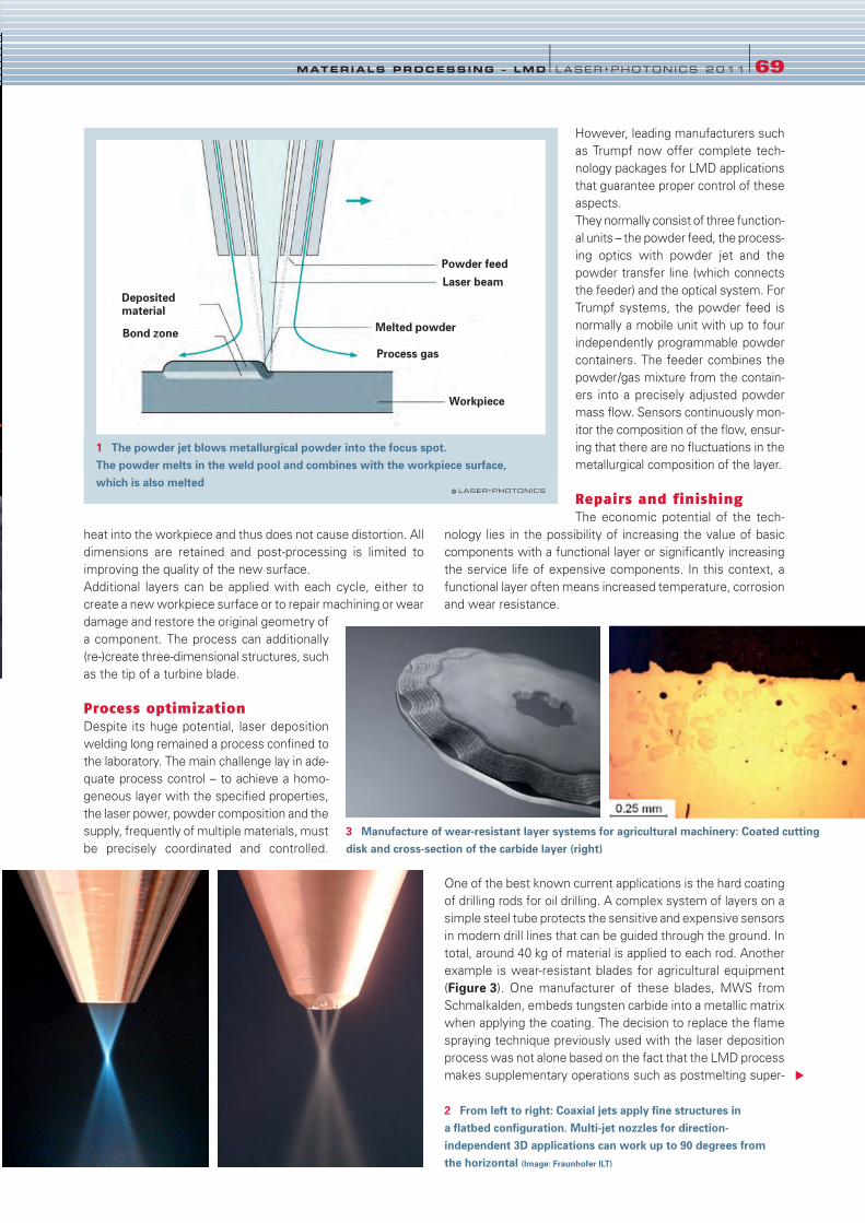
heat into the workpiece and thus does not cause distortion. All
dimensions are retained and post-processing is limited to
improving the quality of the new surface.
Additional layers can be applied with each cycle, either to
create a new workpiece surface or to repair machining or wear
damage and restore the original geometry of
a component. The process can additionally
(re-)create three-dimensional structures, such
as the tip of a turbine blade.
Process optimization
Despite its huge potential, laser deposition
welding long remained a process confined to
the laboratory. The main challenge lay in ade-
quate process control – to achieve a homo-
geneous layer with the specified properties,
the laser power, powder composition and the
supply, frequently of multiple materials, must
be precisely coordinated and controlled.
However, leading manufacturers such
as Trumpf now offer complete tech-
nology packages for LMD applications
that guarantee proper control of these
aspects.
They normally consist of three function-
al units – the powder feed, the process-
ing optics with powder jet and the
powder transfer line (which connects
the feeder) and the optical system. For
Trumpf systems, the powder feed is
normally a mobile unit with up to four
independently programmable powder
containers. The feeder combines the
powder/gas mixture from the contain-
ers into a precisely adjusted powder
mass flow. Sensors continuously mon-
itor the composition of the flow, ensur-
ing that there are no fluctuations in the
metallurgical composition of the layer.
Repairs and finishing
The economic potential of the tech-
nology lies in the possibility of increasing the value of basic
components with a functional layer or significantly increasing
the service life of expensive components. In this context, a
functional layer often means increased temperature, corrosion
and wear resistance.
One of the best known current applications is the hard coating
of drilling rods for oil drilling. A complex system of layers on a
simple steel tube protects the sensitive and expensive sensors
in modern drill lines that can be guided through the ground. In
total, around 40 kg of material is applied to each rod. Another
example is wear-resistant blades for agricultural equipment
(Figure 3). One manufacturer of these blades, MWS from
Schmalkalden, embeds tungsten carbide into a metallic matrix
when applying the coating. The decision to replace the flame
spraying technique previously used with the laser deposition
process was not alone based on the fact that the LMD process
makes supplementary operations such as postmelting super-
MATERIALS PROCESSING – LMD l LASER+PHOTONICS 2011 l69
1 The powder jet blows metallurgical powder into the focus spot. The powder melts in the weld pool and combines with the workpiece surface, which is also melted
© LASER+PHOTONICS
2 From left to right: Coaxial jets apply fine structures in a flatbed configuration. Multi-jet nozzles for direction-independent 3D applications can work up to 90 degrees from the horizontal (Image: Fraunhofer ILT)
3 Manufacture of wear-resistant layer systems for agricultural machinery: Coated cuttingdisk and cross-section of the carbide layer (right)
V
Powder feed
Laser beam
Melted powder
Workpiece
Depositedmaterial
Bond zone
Process gas
68-70_LPX110011_LPX11 15.12.2010 18:23 Uhr Seite 69
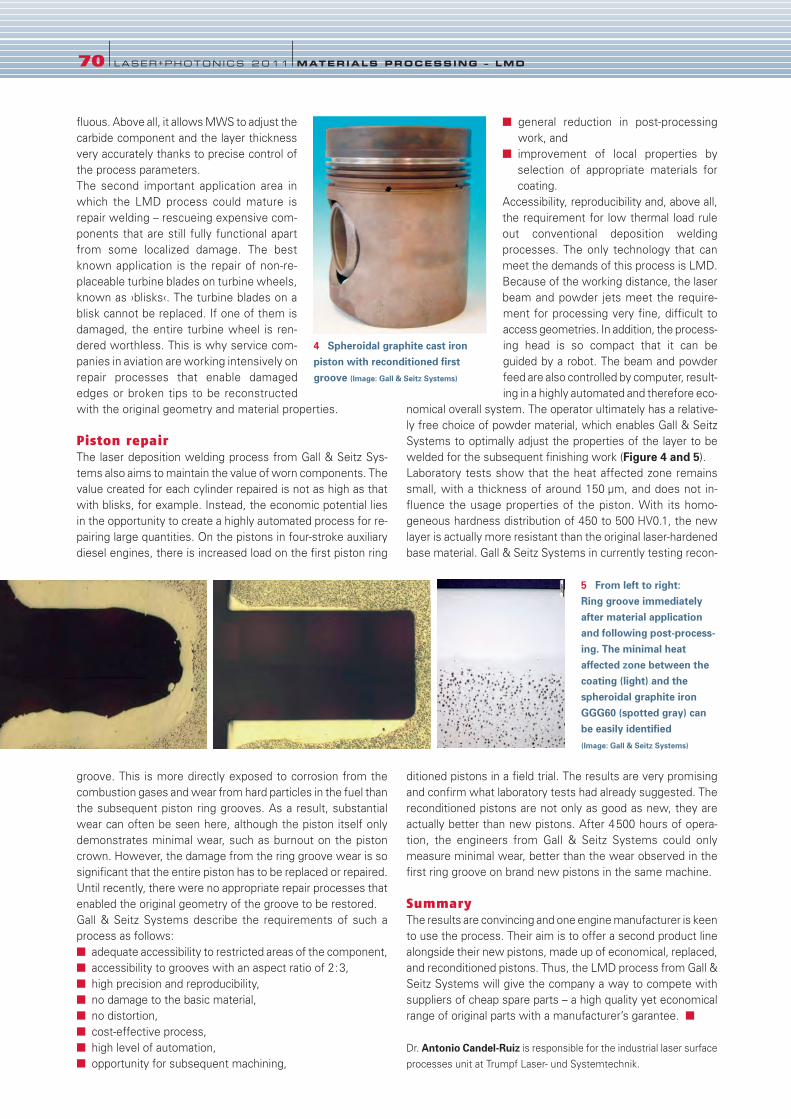
fluous. Above all, it allows MWS to adjust the
carbide component and the layer thickness
very accurately thanks to precise control of
the process parameters.
The second important application area in
which the LMD process could mature is
repair welding – rescueing expensive com-
ponents that are still fully functional apart
from some localized damage. The best
known application is the repair of non-re-
placeable turbine blades on turbine wheels,
known as ›blisks‹. The turbine blades on a
blisk cannot be replaced. If one of them is
damaged, the entire turbine wheel is ren-
dered worthless. This is why service com-
panies in aviation are working intensively on
repair processes that enable damaged
edges or broken tips to be reconstructed
with the original geometry and material properties.
Piston repair
The laser deposition welding process from Gall & Seitz Sys-
tems also aims to maintain the value of worn components. The
value created for each cylinder repaired is not as high as that
with blisks, for example. Instead, the economic potential lies
in the opportunity to create a highly automated process for re-
pairing large quantities. On the pistons in four-stroke auxiliary
diesel engines, there is increased load on the first piston ring
groove. This is more directly exposed to corrosion from the
combustion gases and wear from hard particles in the fuel than
the subsequent piston ring grooves. As a result, substantial
wear can often be seen here, although the piston itself only
demonstrates minimal wear, such as burnout on the piston
crown. However, the damage from the ring groove wear is so
significant that the entire piston has to be replaced or repaired.
Until recently, there were no appropriate repair processes that
enabled the original geometry of the groove to be restored.
Gall & Seitz Systems describe the requirements of such a
process as follows:
■ adequate accessibility to restricted areas of the component,
■ accessibility to grooves with an aspect ratio of 2:3,
■ high precision and reproducibility,
■ no damage to the basic material,
■ no distortion,
■ cost-effective process,
■ high level of automation,
■ opportunity for subsequent machining,
■ general reduction in post-processing
work, and
■ improvement of local properties by
selection of appropriate materials for
coating.
Accessibility, reproducibility and, above all,
the requirement for low thermal load rule
out conventional deposition welding
processes. The only technology that can
meet the demands of this process is LMD.
Because of the working distance, the laser
beam and powder jets meet the require-
ment for processing very fine, difficult to
access geometries. In addition, the process-
ing head is so compact that it can be
guided by a robot. The beam and powder
feed are also controlled by computer, result-
ing in a highly automated and therefore eco-
nomical overall system. The operator ultimately has a relative-
ly free choice of powder material, which enables Gall & Seitz
Systems to optimally adjust the properties of the layer to be
welded for the subsequent finishing work (Figure 4 and 5).
Laboratory tests show that the heat affected zone remains
small, with a thickness of around 150 µm, and does not in-
fluence the usage properties of the piston. With its homo-
geneous hardness distribution of 450 to 500 HV0.1, the new
layer is actually more resistant than the original laser-hardened
base material. Gall & Seitz Systems in currently testing recon-
ditioned pistons in a field trial. The results are very promising
and confirm what laboratory tests had already suggested. The
reconditioned pistons are not only as good as new, they are
actually better than new pistons. After 4500 hours of opera-
tion, the engineers from Gall & Seitz Systems could only
measure minimal wear, better than the wear observed in the
first ring groove on brand new pistons in the same machine.
Summary
The results are convincing and one engine manufacturer is keen
to use the process. Their aim is to offer a second product line
alongside their new pistons, made up of economical, replaced,
and reconditioned pistons. Thus, the LMD process from Gall &
Seitz Systems will give the company a way to compete with
suppliers of cheap spare parts – a high quality yet economical
range of original parts with a manufacturer’s garantee. ■
Dr. Antonio Candel-Ruiz is responsible for the industrial laser surface
processes unit at Trumpf Laser- und Systemtechnik.
70 l LASER+PHOTONICS 2 0 11 lMATERIALS PROCESSING – LMD
5 From left to right: Ring groove immediatelyafter material applicationand following post-process-ing. The minimal heataffected zone between thecoating (light) and thespheroidal graphite ironGGG60 (spotted gray) canbe easily identified (Image: Gall & Seitz Systems)
4 Spheroidal graphite cast ironpiston with reconditioned firstgroove (Image: Gall & Seitz Systems)
68-70_LPX110011_LPX11 15.12.2010 18:23 Uhr Seite 70

COMPANY PROF ILE l71
GWU-LasertechnikVertriebsgesellschaft mbH Bonner Ring 9
50374 Erftstadt
Germany
Phone +49 (0)22 35 9 55 22-0
Fax +49 (0)22 35 9 55 22-99
www.gwu-group.de
GWU-Lasertechnik:The Experts in Tunable Laser Systems andNon-linear Optics
GWU-Lasertechnik Vertriebsges. mbH was
founded in 1988 as a sales and service organ-
isation for lasers and laser accessories. Start-
ing as an agent for the predecessor of Fujian
Castech Crystals GWU-Lasertechnik started to
develop products around crystals delivered by
these Chinese world-leading specialists for
BBO and LBO. First results were demonstrat-
ed at Laser show 1989 in Munich where GWU
introduced the first commercial BBO-OPO
worldwide pumped by the
third harmonic of a q-switched pulsed Nd:YAG
laser at 355 nm. Since then the OPO technol-
ogy has been permanently improved and ma-
tured by GWU. Now they are offering the
fourth generation of BBO-OPOs suited for a
variety of applications including spectroscopy,
environmental analysis, process control in the
chemical and pharmaceutical industry, and lidar
systems. The product line of OPOs is com-
pleted by useful accessories like a wavemeter
that fully integrates into the OPO installation
and software thus allowing fully automated
wavelength calibration, and frequency con-
verters to cover the UV range efficiently down
to about 205 nm. GWU also integrate Nd:YAG
laser heads and OPOs/harmonic generators on
a common platform or completely sealed hous-
ings some of which have been successfully
used outdoor and in harsh environments.
These systems have no need for extra optical
tables and are easily movable. The pulsed OPO
product line is completed by versions pumped
at 532 nm (2nd harmonic of q-
switched Nd:YAG lasers) or 1064
nm. Non-linear materials used in
these systems include BBO, KN-
bO3, and KTP thus allowing to cov-
er the spectral range between 205
nm and >4000 nm. Customised
solutions are developed and
offered as well.
GWU’s OPOs are available in a
variety of configurations among
which you find broadband and
midband systems as well as a version with a
smooth round beam profile and symmetric low
divergence beam characteristics. Unique fea-
ture of all these BBO-OPOs is the low pump
threshold in combination with the most con-
servative pump scheme on the market ensur-
ing highest reliability and lifetime of the optical
components inside.
Besides these nsec OPOs GWU develop and
manufacture OPOs and harmonic generators
for pumping by commercial lasers in the psec
and fsec regime such as Spectra-Physics
Tsunami lasers.
GWU offer a selected range of third party
products. These include a wide spec-
trum of laser crystals and nonlinear
crystals. Most popular crystals are
BBO, LBO, KTP, KD*P, Nd:YVO4,
Nd:YAG among many others manu-
factuerd by the world-leading com-
pany Castech. Periodically-poled
crystals such as MgO:PPLN, manu-
factured by HC Photonics, available
as bulk or waveguide with a variety of
grating structures (single, multiple, fan-out
chirped,…) are of increasing interest especi-
ally due to their high conversion efficiency for
continuous wave and low power applications.
This portfolio of optical components is com-
plemented by prisms, wave-plates, polarizing
optics and standard items.
Latest members in GWU’s product family are
fiber lasers and ASE products of the leading
manufacturer in this field – NP Photonics.
These products include low phase noise nar-
rowband and ultra-narrowband fiber lasers with
powers from 10 mW to several Watts. The
proprietary in-house fiber production technol-
ogy ensures unsurpassed, and reproducible
quality of the product line.
Due to their superior service and competence
GWU have generated a broad base of satisfied
customers in the industry and in scientific
research laboratories.
FirmenPortr_LPex2011 15.12.2010 15:04 Uhr Seite 71

NUMERIK JENA GmbHIlmstraße 4
07743 Jena
Germany
Phone: +49 (0)3641 47 28 88
Fax: +49 (0)3641 47 28 20
www.numerikjena.de
72 lCOMPANY PROF ILE
The companyNUMERIK JENA draws from over 30 years of
experience in the development, manufacture
and sale of position encoders. The roots of pro-
duction metrology and its associated technol-
ogy for the manufacture of precision scales go
back to Carl Zeiß and Ernst Abbe.
In following this great tradition, the goal of all
our activities is continuous innovation and the
improvement of our products.
We orient ourselves to the demands of the in-
ternational market to which we can react flex-
ibly thanks to the modular character of our en-
coders.
The productsNUMERIK Jena offers posi-
tioning sensors with a wide
variety of options according
to the demands of the ap-
plication.
• High resolution for the pre-
cise dynamics of the ac-
tuator
• High accuracy for accurate
and repeatable positioning
• Low short-range errors for constant and
smooth motion
• Low profile requirement for ease of imple-
mentation and to allow simple integration
with existing mechanics
• Low mass for high acceleration
• High traversing speed for fast positioning and
high productivity
• Customer friendly mounting tolerances for
low assembling costs
• High insensitivity against contamination for
high reliability
Applications• suppliers and users of linear and rotary ac-
tuators
• Production equipment of
semiconducter industry
• linear, rotary and planar di-
rect drives
• torque motors
• coordinate measuring
equipment
• Medical technology
T E C H N I C A L M AG A Z I N E S | T E C H N I C A L BO O K S | O N L I N E S E R V I C E S | S E M I N A R S
Carl Hanser Verlag ·P.O. Box 86 04 20 ·81631 Munich ·Germany ·Tel.: +49/89/99830-0 ·Fax: +49/89/984809 · [email protected] · www.hanser.de
Seminars
Technical Magazines
Online Services
Technical Books
Profound Knowledge in a Flexible Multi-Media System: Since 1928 Hanser Publishers have established themselves as competentproviders of information. With 21 professional magazines, some 200 newbook publications and reprints annually as well as about 2,000 titles instock, Hanser ranks amongst the 10 largest German specialist technico-scientific publishing houses. Specialist seminars and conferences as well as branch services on the Internet supplement what is being offered in the way of information. Read more at www.hanser.de
FirmenPortr_LPex2011 15.12.2010 15:04 Uhr Seite 72

COMPANY PROF ILE l73
COMPANY PROF ILE
FRAMOS GmbHZugspitzstrasse 5 C
82049 Pullach/Munich, Germany
Phone +49 (0) 89 710667-0
Fax +49 (0) 89 710667-66
eMail [email protected]
www.framos.de
FRAMOS Electronics Ltd., UKwww.framos.co.uk
FRAMOS Italia srl, Italywww.framos.it
FRAMOS France, Francewww.framos.fr
FRAMOS has been active in the area of in-
dustrial image processing for the last 30 years
and as an innovative partner provides a broad
range of high-quality components and servic-
es. Along with offering image components
such as sensors, companion chips, camera
modules, cameras and accessories, we pro-
vide a real variety of development support serv-
ices for camera manufacturers and users.
FRAMOS Imaging ComponentsSells our partner companies’ image process-
ing components and systems across the globe.
In our component portfolio, we focus on the
areas of machine vision, medical, traffic and
security and provide you with every possible
component, from sensors to the GigE inter-
face, tailored to your needs.
FRAMOS Engineering Services You have an idea for a camera or an image pro-
cessing system? Your prototype needs to be
developed? Or you’re not happy because the
design is finished but it didn't turn out as you
had hoped? We will support you throughout
the whole value chain of your image process-
ing system. We consider the whole surround-
ing architecture (optics, lighting, mechanics,
server infrastructure, data editing etc.).
FRAMOS Solutions FRAMOS Solutions works in linking our ex-
pertise for system integrators to camera users.
Specialist engineers will support you in imple-
menting your ideas and projects, comprehen-
sively and competently. If you want to use an
image processing system, we will help you to
select the best possible combination of all com-
ponents such as cameras, lenses and lighting,
as well as the right software.
CompoTRON GmbHSandstraße 26
80335 München
Phone: +49 (0)89 538 866-0
Fax: +49 (0)89 538 19377
www.compotron.com
CompoTRONis a pan-European technical representative
and distributor of fiber-optic components for
datacom, telecom (incl. FTTx & PON), In-
dustrial Ethernet, medical and metrology ap-
plications. Working exclusively together with
a small number of carefully selected suppli-
ers, we can provide our customers focused
support and a complementary set of product
portfolios. We strive to establish long term
relationships by providing the best product
support through technical competence.
Our strengths include a dedicated product line
management team with a solid technical back-
ground, short reaction times from committed
sales engineers within each geographical re-
gion and strong and long term relationships
with our suppliers.
Our range of standard products covers
MSA transceivers in form factors 1x9, SFF
and SFP for 200 km FE and 120 km GbE. Op-
tical transceivers for 10 Gb/s to 40 Gb/s appli-
cations in SFP+, XFP and 300-pin footprints.
· Components such as 43 Gb/s balanced
photo-receivers with limiting or linear TIA.
· Analogue components e.g. highly linear
butterfly and coaxial 1 to 6 GHz lasers and pho-
to diodes. High output power/CWDM/DWDM
options.
· Passive fiber-optic components to include
WDM, switches, couplers, hybrids etc.
· Mechanical solutions such as SFP / XFP
cages, heat sinks and clips and SMT host board
electrical connectors.
Customisation, buffer stocks and short lead-times complement our standard service of-
fering.
FirmenPortr_LPex2011 15.12.2010 15:05 Uhr Seite 73

WOLFGANG JOHN
There has been one dominant trend in
electronic and mechatronic products for
a long time now – components are shrink-
ing, yet simultaneously have to do more
and more. Particularly in cars, the addi-
tional sensors and components for
new driver assistance systems,
including their cabling, require
an increasing amount of
space that is not easily
available. They also
make vehicles heav-
ier, which is not
desirable either
– the wiring
harness
for
the BMW
3 Series now
weighs approx-
imately 30 kg.
Then there are the
rising costs for manu-
facturing and installing the
systems, which does not
appeal to the OEM or poten-
tial customers.
In communication technology,
manufacturers are under extreme
pressure to constantly bring new
products to market in a very short time-
frame, primarily in order to maintain their
commercial position. And, of course, in order to suc-
ceed in the market these new products must have a
collection of unique selling points that sets them apart from
the mass of competitors. This calls for MID (molded intercon-
nect devices), a technology that makes new products with
previously unattainable functionality possible.
Increased functionality thanks to MID
MID means that conductors can be attached to three-dimen-
sional plastic components and electronic components can be
arranged in a very small space. This enables chips to be
stylishly stacked in their assembly or aerials for smartphones or
netbooks to be created on the housing in order to save space.
At the same time, integrated functionality also reduces the
number of individual components, eliminating a range of pro-
duction steps and thus automatically saving additional costs and
simultaneously delivering a higher quality of components.
Various methods are available for attaching conductors to the
plastic components. Hot embossing involves a stamp for press-
ing thin, flexible films onto the component. The surplus film is
then removed. The process is simple and it works with a
large number of materials, but it is unsuitable for very fine
conductors and cannot achieve genuine three-dimen-
sionality and more complex circuits. With sandwich
molding, the interconnect device is produced first
from plastic. A second plastic, one that can be
metalized, is only deposited where conductors will
subsequently run. The process allows almost unlimited
design freedom in three dimensions, but the two
molds required make it expensive. Production of fine
conductors is also problematic. The relatively long
lead time before this kind of product can come to
market is also a factor (the lead time for the mold-
ing tools alone is roughly two months).
As in many areas of manufacturing, the incomparable flexibili-
ty of lasers is opening up totally new perspectives in MID. In
this subtractive process, the laser removes layers of metal
74 l LASER+PHOTONICS 2 0 11 lMATERIALS PROCESSING – LDS
Three-dimensional components cut product costs NEW LDS SYSTEM FOR COST-EFFICIENT MASS PRODUCTION.Laser direct structuring (LDS) has previously allowed 3D interconnect devices to be
produced cost-efficiently in small and medium runs or even as individual units. The new
Fusion3D system from LPKF cuts the structuring times and costs to around a third,
thus making three-dimensional LDS interconnect devices attractive for the mass market.
1 The structureactivated androughened bythe laser beam(left) is subse-quently metalcoated
74-76_LPX110012_LPX11 15.12.2010 18:27 Uhr Seite 74

where they are not required, or opens a resist for a subsequent
etching process. The technology prerequisites reliable laser
performance and extensively metalized components.
Laser direct structuring
The laser direct structuring (LDS) process patented by LPKF is
more convincing from both a technical and an economic per-
spective. The LDS process uses a thermoplastic that is doped
with a laser-activated metal/plastic additive. When the laser
beam strikes the plastic, the metal complex breaks down and
forms a roughened track. The metal particles act as seeds for
the subsequent metalization. The laser draws the required struc-
tures onto the component and the conductor layers are then
precisely deposited on these tracks in a electroless plating bath.
Copper, nickel and a gold finish can be applied in turn (Figure 1).
This is where the great flexibility, speed, resolution, and preci-
sion of the laser comes into its own. If the course of the con-
ductors changes, it is only
necessary to send new con-
trol data to the laser unit. This
enables different functional
components to be produced
from a single basic compo-
nent, depending on the de-
sign of the circuits inscribed
on them. And because the control data for the laser can also
be switched during production, an operator can manufacture
small and medium-sized runs cost-efficiently. One-off produc-
tion is not limited by cost or technical grounds either. The path
from prototype to series production is short and cost-effective,
allowing the company to respond quickly to the needs of the
market (Figure 2).
The LDS process has already achieved success in a wide range
of applications. The best known product group is complex aerial
structures for high quality cell phones, PDAs and laptops. The
technique has also proved effective in compact and high per-
formance medical technology, pressure sensors and a coupling
system for digital model railways. A pipette system with au-
tomatic volume detection, a steering wheel switch for the
BMW Z4, the handlebars for the BMW K1300 motorcycle, seat
adjusters, control cabinet modules and solar sensors for cli-
mate control in cars are also produced using LDS technology.
At present, research is even in progress into the production of
multi-layer LDS components.
Cell phones become ever more capable
Increased functionality with an ever smaller volume – this is a
key requirement in the communications industry. Thanks to
LDS, up to twelve aerials can cur-
rently be integrated into a cell phone.
However, cell phone manufacturing
is mass production and demands a
considerably higher throughput
than is normal for small and medium-
sized runs. This is where the new
›Fusion3D‹ laser structuring unit from
LPKF comes into play (Figure 3). Up
to four laser heads work simultane-
ously on a precisely manufactured
granite base plate from seven possi-
ble positions. This increases the
throughput compared to previous
systems by up to five times and cuts
the processing time by up to 75 per-
cent. Feed times and component
rotation are eliminated.
The standard version of the Fusion3D
has a laser focus of 65 µm diameter.
This enables conductors with a width
MATERIALS PROCESSING – LDS l LASER+PHOTONICS 2011 l75
2 From a simple molded part to a fully equipped three-dimensional interconnect device
LPKF Laser & Electronics AG 30827 Garbsen, Germany
Tel. +49 (0)5131 7095-0
www.lpkf.de
CONTACT
Sensors & ImagingLow Defect Solutions for Optical Packaging applications
Optics Balzers AG Balzers/LiechtensteinOptics Balzers Jena GmbH Jena/Germany
www.opticsbalzers.com
V
74-76_LPX110012_LPX11 15.12.2010 18:27 Uhr Seite 75
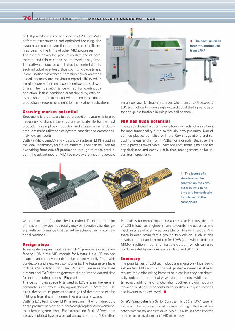
of 150 µm to be realized at a spacing of 200 µm. With
different laser sources and optimized focusing, the
system can create even finer structures, significant-
ly surpassing the limits of other MID processes.
The system saves the production data and all para-
meters, and this can then be retrieved at any time.
The software supplied distributes the control data to
each individual laser head, thus optimizing cycle times.
In conjunction with robot automation, this guarantees
speed, accuracy and maximum reproducibility while
simultaneously minimizing personnel costs and down-
times. The Fusion3D is designed for continuous
operation. It thus combines great flexibility, efficien-
cy and short times to market with the option of mass
production – recommending it for many other applications.
Growing market potential
Because it is a software-based production system, it is only
necessary to change the structure template file for the next
product. This simplifies production and ensures minimal down-
time, optimum utilization of system capacity and correspond-
ingly low unit costs.
With its ›MicroLine3D‹ and ›Fusion3D‹ systems, LPKF supplies
the ideal technology for future markets. They can be used for
everything from one-off production through to mass-produc-
tion. The advantages of MID technology are most noticeable
where maximum functionality is required. Thanks to the third
dimension, they open up totally new perspectives for design-
ers, with performance that cannot be achieved using conven-
tional methods.
Design steps
To make developers’ work easier, LPKF provides a direct inter-
face to LDS in the MID module for Nextra. Here, 3D molded
shapes can be conveniently designed and virtually fitted with
conductors and electronic components. The features available
include a 3D splitting tool. The LPKF software uses the three
dimensional CAD data to generate the optimized control data
for the structuring process (Figure 4).
The design rules specially tailored to LDS explain the general
parameters and assist in laying out the circuit. With the LDS
rules, the optimum process advantages of the method can be
achieved from the component layout phase onwards.
With its LDS technology, LPKF is heading in the right direction,
as the production method is increasingly replacing conventional
manufacturing processes. For example, the Fusion3D systems
already installed have increased capacity to up to 100 million
aerials per year. Dr. Ingo Bretthauer, Chairman of LPKF, expects
LDS technology to increasingly expand out of the high-end sec-
tor and gain a foothold in mid-price cell phones.
MID has huge potential
The key to LDS is ›function follows form‹ – which not only allows
for new functionality but also visually new products. Use of
defined plastics complies with the RoHS regulations and re-
cycling is easier than with PCBs, for example. Because the
entire process takes place under one roof, there is no need for
sophisticated and costly just-in-time management or for in-
coming inspections.
Particularly for companies in the automotive industry, the use
of LDS is ideal, as engineers have to combine electronics and
mechanics as efficiently as possible, while saving space. And
there is even more fertile ground to work on, such as the
development of aerial modules for UWB (ultra wide band) and
MIMO (multiple input and multiple output), which can also
combine satellite services such as GPS and SDARS.
Summary
The possibilities of LDS technology are a long way from being
exhausted. MID applications will probably never be able to
replace the entire wiring harness on a car, but they can drasti-
cally reduce its complexity, weight and costs, while simul-
taneously adding new functionality. LDS technology not only
replaces existing components, but also allows unique functions
and layouts to be achieved. ■
Dr. Wolfgang John is a Senior Consultant in LDS at LPKF Laser &
Electronics. He has spent his entire career working at the boundaries
between chemistry and electronics. Since 1994, he has been involved
in the ongoing development of MID technology.
76 l LASER+PHOTONICS 2 0 11 lMATERIALS PROCESSING – LDS
4 The layout of astructure can beadapted on the com-puter in little to notime and immediatelytransferred to thecomponent
3 The new Fusion3Dlaser structuring unitfrom LPKF
74-76_LPX110012_LPX11 15.12.2010 18:27 Uhr Seite 76

Versatile rangeLED linear lighting. Vision & Control is
introducing a new linear lighting range
›LLL7‹, suited for line scan as well as area
scan cameras. The LED lights produce a
uniformly illuminated line. For the most
intense brightness, the light can be fo-
cused to a tight line illumination with up
to 130 000 lux, using special linear lens-
es. The lights do not need active cooling
devices. Special integrated optical com-
ponents ensure homogeneity in excess
of 90 percent while maintaining a high
light efficiency. They are therefore suit-
ed for extremely fast line scan camera
applications with diffuse back lighting as
well as for demanding applications with
incident lighting, for instance for the in-
spection of shiny surfaces – thanks to the
adjustable and exchangeable rod lenses,
which allow adjustment to various
working distances and line widths. This
compact range, with a cross section of
9x12 mm2, is offered in lengths of 25 to
250 mm, with 25 mm increments. The
linear lights are available in nine different
wavelengths, from ultraviolet (395 nm)
to infrared (950 nm).
www.vision-control.com
Bright scannig light LED line illumination. Chromasens has
optimized their ›Corona‹ LED illumination
system, a photometrically optimized and
regulated LED line illumination system
with a flexible cooling concept and espe-
cially designed for applications with line
scan cameras. The high-power LEDs with
an illuminance of well over 1 000 000 lux
promise to satisfy the highest quality
requirements with respect to brightness
and illuminance. The LEDs are driven by
an external controller; the operating
current is set via an integrated micro-
controller. The brightness can be adjust-
ed via PC with the operating software
›Illumination Setup Tool‹ (IST).
www.chromasens.de
Analysis of filiform corrosionScanning macroscope. Filiform corro-
sion is a special form of corrosion that
occurs on coated aluminum and low alloy
steels. Interaction with water and oxygen
cause corrosion cells to form between the
metal surface and the coating, which
slowly migrate, leaving behind filiform in-
filtration and causing major damage. The
newly developed filiform scanner from
Schäfter+Kirchhoff automates the analy-
sis of standardized test plates using a
resolution of 6 megapixels. The CCD line
scan camera with integrated bright field
illumination ensures very high contrast
images of the filiform infiltration. The soft-
ware identifies the characteristic struc-
tures from the digital images obtained and
evaluates them objectively against the
standards. This enables quantifiable
results to be obtained and documented
extremely quickly.
www.SuKHamburg.de
PRODUCT MARKETPLACE l LASER+PHOTONICS 2011 l77
Please see us at Photonics West,South Hall Booth 2523
77-79_LPX_Produkte_LPX11 15.12.2010 18:32 Uhr Seite 77
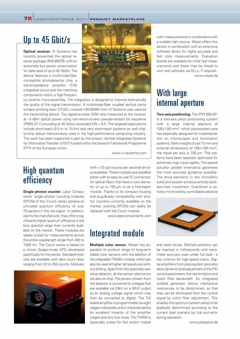
High quantumefficiency Single photon counter. Laser Compo-
nents’ single photon counting modules
(SPCM) of the ‹Count‹ series achieve an
unrivaled quantum efficiency of over
70 percent in the red region. In addition,
claims the manufacturer, they offer a sig-
nificantly higher quantum efficiency in the
blue spectral range than currently avail-
able on the market. These modules are
ideally suited for measurements across
the entire wavelength range from 400 to
1000 nm. The Count series is based on
a silicon Geiger-mode APD developed
specifically for this series. Standard mod-
ules are available with dark count rates
ranging from 20 to 250 counts. Modules
with <10 cps (counts per second) are al-
so available. These modules are available
either with an easy-to-use FC connection
for optical fibers that have a core diame-
ter of up to 105 µm or as a free-beam
module. Thanks to its compact housing
and plug-&-play compatibility with pho-
ton counters currently available on the
market, existing SPCMs can easily be
replaced with the Count module.
www.lasercomponents.com
Integrated moduleMultiple color sensor. Mazet has ex-
panded its product range of long-term
stable color sensors with the addition of
the integrated ›TIAM4‹ module, which can
also be used at higher temperatures with-
out drifting. Apart from the spectrally sen-
sitive detector, all the sensor electronics
are also on-chip. The photon stream from
the detector is converted to voltages that
are available via S&H on a MUX output
as an analog voltage signal which may
then be converted to digital. The TIA
based amplifier is programmable via eight
stages individually and is characterized by
its excellent linearity of the amplifier
stages and very low noise. The TIAM4 is
especially suited for fast and/or mobile
color measurements in combination with
a suitable light source. Mazet offers this
sensor in combination with an extensive
software library for highly accurate and
fast color measurements. Evaluation
boards are available for initial test meas-
urements and these may be linked to
own test software via DLLs, if required.
www.mazet.de
With large internal aperture Two-axis positioning. The ›PXY 500 AP‹
is a two-axis piezo positioning system
with a large internal aperture of
100x100 mm2, which piezosystem jena
has especially designed for implementa-
tion on microscopes and illumination
systems. With a height of just 15 mm and
external dimensions of 185x185 mm2,
the travel per axis is 700 µm. The sys-
tems have been specially optimized for
extremely high z-axis rigidity. The special
actuator parallel kinematics garantees
the most accurate guidance possible.
The drive elements in the monolithic
solid joint system produce entirely back-
lash-free movement. Overshoot is ac-
tively minimized by controllable advance
and reset forces. Defined positions can
be reached in milliseconds with nano-
meter accuracy even under full load – a
key criterion for high-speed scans. Digi-
tal amplifiers from piezosystem jena also
allow dynamic local adjustment of the PID
control parameters, the rise limitation and
notch filter bandwidth. An integrated
wobble generator allows mechanical
resonances to be determined, so that
they can be eliminated from the control
signal by notch filter adjustment. This
enables the optimum system setup to be
gradually determined according to the
current load scenario by trial and error
during operation.
www.piezojena.de
78 l LASER+PHOTONICS 2 0 11 lPRODUCT MARKETPLACE
Up to 45 Gbit/s Optical receiver. VI Systems has
recently presented the optical re-
ceiver package ›R40-850TB‹ with an
extremely low power consumption
for data rates of up to 45 Gbit/s. The
device features a multimode-fiber
compatible photodetector chip, a
transimpedance amplifier (TIA)
integrated circuit and the matching
components within a high-frequen-
cy ceramic micro-assembly. The integration is designed to improve dramatically
the quality of the signal transmission. A multimode-fiber coupled vertical cavity
surface emitting laser (VCSEL) module V40-850M from VI Systems was used as
the transmitting device. The signal-to-noise (S/N) ratio measured at the receiver
at –3 dBm optical power using non-return-to-zero pseudo-random bit sequence
(PRBS 27-1) encoding at 40 Gbit/s exceeded S/N = 6.5. The targeted applications
include short-reach (0.5 m to 10 km) and very short-reach systems as well chip-
to-chip optical interconnects used in the high-performance computing industry.
The work has been supported in part by the project ›Vertical Integrated Systems
for Information Transfer‹ (VISIT) funded within the Seventh Framework Programme
(FP7) of the European Union.
www.v-i-systems.com
77-79_LPX_Produkte_LPX11 15.12.2010 18:33 Uhr Seite 78
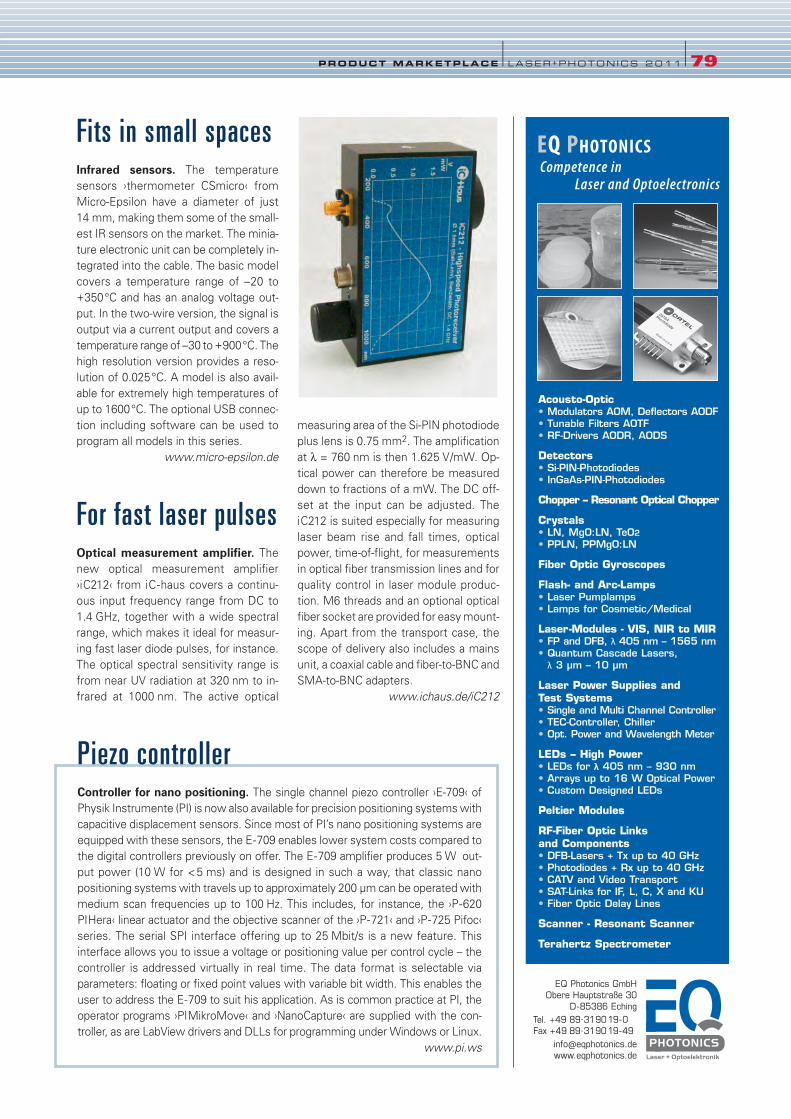
Fits in small spaces Infrared sensors. The temperature
sensors ›thermometer CSmicro‹ from
Micro-Epsilon have a diameter of just
14 mm, making them some of the small-
est IR sensors on the market. The minia-
ture electronic unit can be completely in-
tegrated into the cable. The basic model
covers a temperature range of –20 to
+350°C and has an analog voltage out-
put. In the two-wire version, the signal is
output via a current output and covers a
temperature range of –30 to +900°C. The
high resolution version provides a reso-
lution of 0.025°C. A model is also avail-
able for extremely high temperatures of
up to 1600°C. The optional USB connec-
tion including software can be used to
program all models in this series.
www.micro-epsilon.de
For fast laser pulsesOptical measurement amplifier. The
new optical measurement amplifier
›iC212‹ from iC-haus covers a continu-
ous input frequency range from DC to
1.4 GHz, together with a wide spectral
range, which makes it ideal for measur-
ing fast laser diode pulses, for instance.
The optical spectral sensitivity range is
from near UV radiation at 320 nm to in-
frared at 1000 nm. The active optical
measuring area of the Si-PIN photodiode
plus lens is 0.75 mm2. The amplification
at λ = 760 nm is then 1.625 V/mW. Op-
tical power can therefore be measured
down to fractions of a mW. The DC off-
set at the input can be adjusted. The
iC212 is suited especially for measuring
laser beam rise and fall times, optical
power, time-of-flight, for measurements
in optical fiber transmission lines and for
quality control in laser module produc-
tion. M6 threads and an optional optical
fiber socket are provided for easy mount-
ing. Apart from the transport case, the
scope of delivery also includes a mains
unit, a coaxial cable and fiber-to-BNC and
SMA-to-BNC adapters.
www.ichaus.de/iC212
PRODUCT MARKETPLACE l LASER+PHOTONICS 2011 l79
EQ PHOTONICSCompetence in Laser and Optoelectronics
EQ Photonics GmbH Obere Hauptstraße 30
D-85386 Eching Tel. +49 89·319019-0 Fax +49 89·319019-49
[email protected] www.eqphotonics.de
Acousto-Optic Modulators AOM, Deflectors AODF Tunable Filters AOTF RF-Drivers AODR, AODS
Detectors Si-PIN-Photodiodes InGaAs-PIN-Photodiodes
Chopper – Resonant Optical Chopper
Crystals LN, MgO:LN, TeO2 PPLN, PPMgO:LN
Fiber Optic Gyroscopes
Flash- and Arc-Lamps Laser Pumplamps Lamps for Cosmetic/Medical
Laser-Modules - VIS, NIR to MIR FP and DFB, λ 405 nm – 1565 nm Quantum Cascade Lasers,
λ 3 μm – 10 μm
Laser Power Supplies and Test Systems Single and Multi Channel Controller TEC-Controller, Chiller Opt. Power and Wavelength Meter
LEDs – High Power LEDs for λ 405 nm – 930 nm Arrays up to 16 W Optical Power Custom Designed LEDs
Peltier Modules
RF-Fiber Optic Links and Components DFB-Lasers + Tx up to 40 GHz Photodiodes + Rx up to 40 GHz CATV and Video Transport SAT-Links for IF, L, C, X and KU Fiber Optic Delay Lines
Scanner - Resonant Scanner
Terahertz Spectrometer
Piezo controller Controller for nano positioning. The single channel piezo controller ›E-709‹ of
Physik Instrumente (PI) is now also available for precision positioning systems with
capacitive displacement sensors. Since most of PI’s nano positioning systems are
equipped with these sensors, the E-709 enables lower system costs compared to
the digital controllers previously on offer. The E-709 amplifier produces 5 W out-
put power (10 W for <5 ms) and is designed in such a way, that classic nano
positioning systems with travels up to approximately 200 µm can be operated with
medium scan frequencies up to 100 Hz. This includes, for instance, the ›P-620
PIHera‹ linear actuator and the objective scanner of the ›P-721‹ and ›P-725 Pifoc‹
series. The serial SPI interface offering up to 25 Mbit/s is a new feature. This
interface allows you to issue a voltage or positioning value per control cycle – the
controller is addressed virtually in real time. The data format is selectable via
parameters: floating or fixed point values with variable bit width. This enables the
user to address the E-709 to suit his application. As is common practice at PI, the
operator programs ›PIMikroMove‹ and ›NanoCapture‹ are supplied with the con-
troller, as are LabView drivers and DLLs for programming under Windows or Linux.
www.pi.ws
77-79_LPX_Produkte_LPX11 15.12.2010 18:33 Uhr Seite 79

80 l LASER+PHOTONICS 2 0 11 l TRADE DIRECTORY
A. Laser beam sources
Diode laser modules
LIMO LissotschenkoMikrooptik GmbHwww.limo.de
Diode laser systems
LIMO LissotschenkoMikrooptik GmbHwww. limo.de
High-performance diodelasers
LIMO LissotschenkoMikrooptik GmbHwww. limo.de
Oscillators, optical para-metric
GWU-LasertechnikPhone +49(0)2235 955220eMail [email protected] www.gwu-group.de/laser
Solid state lasers, diodepumped
www.gwu-group.de/laser
Solid state lasers, others
www.gwu-group.de/laser
B. Laser system components and radiation protection
Beam guidance systems
Berliner Glas KGaAPhone: +4930/[email protected]
Beam splitters andexpanders
Berliner Glas KGaAPhone: +4930/[email protected]
Protective windows forlaser welding equipment
B + M Optik GmbHAm Fleckenb.20, 65549 LimburgPh.+49(0)6431 9860-0, [email protected]
Systems components,other
Berliner Glas KGaAPhone: +4930/[email protected]
B + M Optik GmbHAm Fleckenb.20, 65549 LimburgPh.+49(0)6431 9860-0, [email protected]
C. Laser components
Crystals
www.gwu-group.de/laser
Laser components, other
Berliner Glas KGaAPhone: +4930/[email protected]
Mirrors
Berliner Glas KGaAPhone: +4930/[email protected]
D. Opto-electronic components
IR optical elements
Berliner Glas KGaAPhone: +4930/[email protected]
H. Raw materials
Crystals, non linear
GWU-LasertechnikPhone +49(0)2235 955220eMail [email protected] www.gwu-group.de/laser
Crystals, other
www.gwu-group.de/laser
Laser crystals
www.gwu-group.de/laser
I. Processed components
Beam splitters
B + M Optik GmbHAm Fleckenb.20, 65549 LimburgPh.+49(0)6431 9860-0, [email protected]
Components, micro-optical
B + M Optik GmbHAm Fleckenb.20, 65549 LimburgPh.+49(0)6431 9860-0, [email protected]
LIMO LissotschenkoMikrooptik GmbHwww. limo.de
Components, optical,other
Berliner Glas KGaAPhone: +4930/[email protected]
B + M Optik GmbHAm Fleckenb.20, 65549 LimburgPh.+49(0)6431 9860-0, [email protected]
www.gwu-group.de/laser
Filters, optical
B + M Optik GmbHAm Fleckenb.20, 65549 LimburgPh.+49(0)6431 9860-0, [email protected]
Lenses, optical
B + M Optik GmbHAm Fleckenb.20, 65549 LimburgPh.+49(0)6431 9860-0, [email protected]
Mirrors, optical
B + M Optik GmbHAm Fleckenb.20, 65549 LimburgPh.+49(0)6431 9860-0, [email protected]
Mirrors, optical flat
B + M Optik GmbHAm Fleckenb.20, 65549 LimburgPh.+49(0)6431 9860-0, [email protected]
TRADEDIRECTORYProducts – Technologies – Services
A. Laser-beam sources
B. Laser system components and radiation protection
C. Laser components
D. Opto-electronic components
E. Electro-optics
F. Acousto-optics
G. Display technology
H. Raw materials
I. Processed components
J. Optical systems
K. Opto-mechanics
L. Optical production
M. Services
N. Optical systems arranged by branch of industry
O. Optical transmission technology, fibre-optic technology
P. System integration
Q. System design – material design
R. Laser materials processing, system peripherals,
laser-assisted product development and construction
S. Holographic systems/accessoires
T. Optical measuring and testing technology, sensor technology
GROUPS
80-81_bqn_LPex11 15.12.2010 12:46 Uhr Seite 80

Polarizers
Berliner Glas KGaAPhone: +4930/[email protected]
Prisms, optical
B + M Optik GmbHAm Fleckenb.20, 65549 LimburgPh.+49(0)6431 9860-0, [email protected]
www.gwu-group.de/laser
Wave plates
www.gwu-group.de/laser
J. Optical systems
Camera lenses
Berliner Glas KGaAPhone: +4930/[email protected]
Cameras
Berliner Glas KGaAPhone: +4930/[email protected]
Objectives
B + M Optik GmbHAm Fleckenb.20, 65549 LimburgPh.+49(0)6431 9860-0, [email protected]
Oculars
B + M Optik GmbHAm Fleckenb.20, 65549 LimburgPh.+49(0)6431 9860-0, [email protected]
Systems, optical, other
Berliner Glas KGaAPhone: +4930/[email protected]
LIMO LissotschenkoMikrooptik GmbHwww. limo.de
L. Optics production
Coatings, optical
Berliner Glas KGaAPhone: +4930/[email protected]
B + M Optik GmbHAm Fleckenb.20, 65549 LimburgPh.+49(0)6431 9860-0, [email protected]
M.Services
Application development,application laboratories
LIMO LissotschenkoMikrooptik GmbHwww. limo.de
N. Optical systems arranged by branch of industrie
Optical systems for otherbranches
Berliner Glas KGaAPhone: +4930/[email protected]
Optical systems forprinting technology and
Berliner Glas KGaAPhone: +4930/[email protected]
Optical systems for thesemi-conductors industry
Berliner Glas KGaAPhone: +4930/[email protected]
Optical systems forscience and research
Berliner Glas KGaAPhone: +4930/[email protected]
O.Optical transmission technology, Fiber-optic technology
Fibre bundles
LightGuideOpticsGermanyPhone +49 2226 158516eMail [email protected]
Fibres, general
LightGuideOpticsGermanyPhone +49 2226 158516eMail [email protected]
Fibre-optic connections
LightGuideOpticsGermanyPhone +49 2226 158516eMail [email protected]
R. Laser materials processing, system peripherals, Laser-assisted product development andconstruction
Fibre-optic systems
LightGuideOpticsGermanyPhone +49 2226 158516eMail [email protected]
Laser material processingsystems, other
LIMO LissotschenkoMikrooptik GmbHwww. limo.de
Laser microprocessingsystems
LIMO LissotschenkoMikrooptik GmbHwww. limo.de
Laser surface treatmentsystems
LIMO LissotschenkoMikrooptik GmbHwww. limo.de
T. Optical metrology and testing technology, sensor technology
Autocollimators
www.moeller-wedel-optical.com
Fibre-optic detectiondevices
LightGuideOpticsGermanyPhone +49 2226 158516eMail [email protected]
Interferometers
www.moeller-wedel-optical.com
Test systems for opticalcomponents
www.moeller-wedel-optical.com
TRADE DIRECTORY lLASER+PHOTONICS 2011 l81
80-81_bqn_LPex11 15.12.2010 12:46 Uhr Seite 81
82 l LASER+PHOTONICS 2 0 11 l INDEX
Alfred Wegener Institute 16
Arges GmbH, Wackersdorf 38Ascona 6
Astrophysical Institute Potsdam 19
Automation Technology 46
B&M Optik 15
Basler AG, Ahrensburg 35, 46
Baumer 41
Berliner Glas KGaA HerbertKubatz GmbH & Co., Berlin 13
Berliner Glas Medical
Applications 14
Centrotherm 63
China Sunenergy 63
Chromasens 77
Cmosis 46
CompoTron GmbH, München 73
CrystaLaser 27
DLR Institute for Robotics and
Mechatronics 44
Docter Optics GmbH, Neustadt a.d. Orla 14, 37
e2v 41
EQ Photonics GmbH, Eching 79European Southern
Observatory (ESO) 30
European Union 78
Expocentr Fairgrounds/Photonica 64
Filtrop AG, Balzers/FL 31Fisba Optik AG,
St. Gallen/CH 10Framos GmbH, Pullach 73Fraunhofer Institute for
Applied Optics & Precision
Engineering (IOF) 8, 60
Fresnel Optics GmbH,Apolda 36
Gall & Seitz Systems 68
GD Optical Competence GmbH, Sinn 26
GWU-Lasertechnik Vertriebsgesellschaft mbH,Erftstadt 71
Hanser Verlag, München 72Hasselblad 4
High Q Laser 26
IB/E Optics 47
IC-Haus GmbH, Bodenheim 45, 79
IDS Imaging DevelopmentSystems GmbH, Obersulm 27, 41
IMM Photonics 26
IMT Masken und Teilungen AG,Greifensee/CH 67
innoFSPEC Potsdam Center for
Innovation Competence 19
Instrument Systems GmbH,München 24
IntergraphZ/I 5
Jenoptik Laser 27
Jenoptik Optical Systems 40
Kappa 40
Kodak 41
Laser 2000 GmbH, Weßling 22, 27, 39
Laser Components GmbH, Olching 23, 78
Laseroptik GmbH, Garbsen 60, back cover
LaserVision GmbH & Co.KG,Fürth 14
Lasos Lasertechnik GmbH, Jena 33
Layertec GmbH, Mellingen 11LEJ Leistungselektronik
Jena GmbH, Jena 24Leoni Fiber Optics GmbH,
Neuhaus-Schierschnitz 21, 43, 57
Leoni Fiber Tech 20
Limo 27
LPKF Laser & Electronics 74
Lumics 26
m2k-laser 35
Manz 63
Matrix Vision 47
Mazet 78
MechOnics AG, München 66Meerstetter Engineering GmbH,
Rubigen/CH 33Messe München/Laser World
of Photonics inside back coverMicos GmbH, Eschbach 36Micro-Epsilon, Ortenburg 3, 79
Mikrotron 40
Möller-Wedel Optical GmbH,Wedel 56
MVTec Software 39
MWS 69
NanoFocus AG, Oberhausen 12Numerik Jena GmbH, Jena 72Omicron Laserage
Laserprodukte GmbH, Rodgau 65
Optenso, Heerbrugg/CH 54Optic Balzers AG,
Balzers/FL 14, 25, 75Optocraft GmbH, Erlangen 40optoSiC GmbH, Baden-Baden 61Owis GmbH,
Staufen front cover, 52
PCO AG, Kelheim 29, 45
Physik Instrumente GmbH &Co.KG, Karlsruhe 19, 79
piezosystem jena 78
Polytec GmbH, Waldbronn 11Primes GmbH, Pfungstadt 47Qioptiq Photonics GmbH &
Co.KG, Göttingen 7, 16
Raylase AG, Wessling 66Rofin Baasel Lasertech 63
Roth & Rau 63
Schäfter + Kirchhoff GmbH,Hamburg 15, 16, 77
Schmid 63
SensoPart Industriesensorik 39
Sill Optics 15,
Sios Meßtechnik GmbH, Ilmenau 13
Spectros AG, Ettingen/CH 53Spetec GmbH, Erding 63SphereOptics GmbH,
Uhldingen-Mühlhofen 46Stemmer Imaging GmbH,
Puchheim 56SVS-Vistek GmbH, Seefeld 41, 53Texas Instruments 47
Time-Bandwidth Products AG,Zürich/CH 77
Toptica Photonics AG, Gräfelfing 30, 41
Trioptics GmbH, Wedel 15, 22Trumpf Laser- &
Systemtechnik 68
University of Giessen 59
University of Texas, Austin,
TX/USA 20
VDS Vosskühler 39
VI Systems 78
Vision & Control 77
Vistas 46
VRmagic 47
WZW Optic AG, Balgach/CH 55Z-Laser Optoelektronik GmbH,
Freiburg 31Carl Zeiss 4, 44
Zünd Präzisions-Optik AG,Diepoldsau/CH 45
ADVERTISERS are highlighted
PERSONS Boyle, Willard 18
Bretthauer, Ingo 76
Cairós Barreto, Luz Marina 18
Candel-Ruiz, Antonio 68
Diete, Norbert 4
Eberhardt, Ramona 8
Ebert, Wolfgang 58
Engstler, M. 43
Fahlbusch, Jürgen 4
Flinn, Gregory 3
Friedmann, Patrick 32
Gilly, Jürgen 32
Gross, Tobias 58
Hendel, Richard 62
Holst, Gerhard 42
John, Wolfgang 74
Kaenders, Wilhelm 28
Kao, Charles 18
Kelemen, Márc 32
Kelz, Andreas 18
Lang, Marion 28
Roth, Martin M. 18
Schäffler, Thomas 16
Weinert, Andreas 21
Zeitlhack, Georg 16
Zwicky, Franz 20
ADVERTISERS, COMPANIES AND INSTITUTIONS
■ Editor-in-Chief Dr. Gregory Flinn (responsible)
Kolbergerstrasse 22
81679 Munich, Germany
Tel. +49 89 99830-650
Fax +49 89 99830-157
■ Editors Liane Thiele
Tel. +49 89 99830-612
■ Publisher Carl Hanser Verlag GmbH & Co. KG
Kolbergerstrasse 22
81679 Munich, Germany
P.O. Box 860420
81631 Munich, Germany
Tel. +49 89 99830-0
Fax +49 89 984809
www.hanser.de
■ Managing Directors Wolfgang Beisler, Stephan D. Joss,
Michael Krüger
■ Advertisement Manager Martin Ricchiuti (responsible)
Tel. +49 89 99830-686
Fax +49 89 99830-623
Miriam Weihe (Dispo)
Tel. +49 89 99830-216
Fax +49 89 99830-623
■ Layout and Production Thomas West
Tel. +49 89 99830-422
Hadrian Zett (Production Manager)
Tel. +49 89 99830-420
■ Print Firmengruppe APPL, sellier druck GmbH,
Angerstrasse 54
85354 Freising, Germany
Printed in Germany.
■ Copyright and Publishing Rights The publication and all individual articles
and illustrations contained herein are
protected by copyright.
Upon an article being accepted for pub-
lication, the rights of publication, as well as
the rights of translation, of granting repro-
duction licences, of storage in electronic
retrieval systems, of producing special im-
pressions, photocopies and microcopies
are transferred to the publisher. Any utiliza-
tion thereof outside the limits of the copy-
right act is forbidden without the written
permission of the publisher.
■ Descriptive Names The use of general descriptive names, pro-
prietary names, trade names, commercial
designations or the like in this publication
in no way implies that such names may be
used freely: these are often legally protect-
ed, registered trademarks, even if not de-
signated as such.
While the advice and information in this
journal are believed to be true and accu-
rate at the date of its going to press,
neither the authors, the editors, nor the
publisher can accept any legal
responsibility for any errors or omissions
that may be made. The publisher makes
no warranty, express or implied, with
respect to the material contained herein.
© Carl Hanser Verlag, Munich 2011
82_Index_Impress_fin 16.12.2010 19:02 Uhr Seite 82

LIGHT APPLIED
THIS YEAR IN MAY!
23–26 MAY 2011
EVERYONE WHO IS
WHO WILL YOU MEET
AT A LEADING TRADE FAIR?
A LEADER.It is the most important marketplace and a think tank at the same time: As the world’s leading trade fair, LASER World of PHOTONICS brings together all the key players in science and industry. It revolves around both research and applications and gives you a complete market over-view and access to concrete solutions for your daily business. Innovations and trends? This is where they are presented fi rst. Practical orientation? Experience it in our sector-specifi c application panels. Take the lead with us and register online at www.world-of-photonics.net.
20TH INTERNATIONAL TRADE FAIR AND CONGRESS FOR OPTICAL TECHNOLOGIES—COMPONENTS, SYSTEMS AND APPLICATIONS
www.world-of-photonics.net
NEWMUNICHTRADE FAIR CENTRE
U3-4 15.12.2010 18:53 Uhr Seite 1

IBS hit it again...
Home of high power coatings and optics
LASEROPTIK GmbHGneisenaustr. 14D-30826 Garbsen
Telefon (051 31 ) 45 97 -0Telefax (051 31 ) 45 97 20e-Mail: [email protected]
eShop + eCatalog: www.laseroptik.de Narrow bandwidth interference filterFilter for intra cavity use in external cavity diode laser. Adjustment of the laser wavelengthby angle tuning.
GDD-optimized broad band mirrorPump mirror for a Ti:sapphire laser with high transmittance at 532 nm and R > 99.9 % @ 680-1100 nm.
Super mirror R > 99.998 % at 633 nm / 0° with lowest scatter losses ( TSb = 1.1 ppm, measured atFraunhofer IOF, Jena ).
Some of our recent
IBS coating results:
With Ion Beam Sputtered (IBS) coatingsLASEROPTIK reliably hits the mark.
If it comes to high precision coating designs,thermal stability, lowest losses and highestreflectivities, our IBS tech nology is the mostadvanced coating method, in order to meetyour specifi cations.
TSb: 1.1 ppm
0
20
40
60
80
100T %
measured
target
500 530 560 590 620 650 680 800nm710 740
0
20
40
60
80
100T %
measuredtarget
791 793 795 797 799 805nm801 803
0
20
40
60
80
100T %
GDD
transmission
500 860560 1100620 980680 800 nm920740-500
-300
-100
100
300
500
GD
D (
fs2)
BU
TZ
KE
_ _ _ _ _ _U3-4 15.12.2010 18:53 Uhr Seite 2