laser scanner-stage synchronization method for high · pdf filelaser scanner-stage...
TRANSCRIPT
JLMN-Journal of Laser Micro/Nanoengineering Vol. 7, No. 2, 2012
231
Laser Scanner-Stage Synchronization Method for High-Speed And Wide-Area Fabrication
Kyunghan Kim*1, Kwangho Yoon*1 Jeong Suh*1, and Jaehoon Lee *1
*1 Dept. of High Density Energy Beam Processing & System, Korea Institute of Machinery & Materials, 104 Sinseongno, Yeseong- gu, Dae-jeon, 305-343, Korea
E-mail: [email protected]
This paper presents an on-the-fly method to synchronize a laser galvanometer scanner and linear stage for fast and wide-area fabrication. The location and velocity information of the linear stage is transferred to the galvanometer scanner control board by an encoder signal. The scanner control board calculates the amount of laser beam movement by subtracting from original CAD data to lin-ear stage movement. The on-the-fly method is different from the existing step and scanning method in that it ensures continuous stage movement and real-time signal transfer between the linear stage and galvanometer scanner. Keywords: Laser, Galvanometer scanner, Linear stage, On-the-fly, Synchronization
1. Introduction
Short-pulsed laser technology allows for material fabri-cation processes using ultra-precision lasers, such as via-hole drilling [1], FPCB (Flexible PCB) cutting [2], and surface texturing [3]. This trend of laser fabrication re-quires a high-speed, wide-area, and dry process due to con-cerns over environmental problems. The galvanometer scanner is being widely used as a marking tool [4]. Recent-ly, it has been applied to many laser material fabrication fields [5]. However, the working field size of this scanner is limited by the focal length of the f-theta objective lens, which is measured from the scanner head to the sample. When the focal length is increased, the working field size of the scanner becomes wider, but the resolution of the scanning field decreases, which can be a drawback for pre-cise fabrication. A hybrid method that involves the use of both a linear stage and a scanner is being considered for wide-area fabrication. The initial approach that has been adopted is known as the step and scanning method. The stage repeatedly moves and stops in steps, and the scanner operates when the stage stops. Therefore, this method caus-es discontinuous quality and increases the fabrication time, because stage motion stops when the scanner is operating. To overcome this problem, a hybrid method that involves the use of both a linear stage and a scanner has recently been developed. Manufacturers of the scanner-stage syn-chronization processing equipment include ESI, LPKF, and AEROTECH. Electro Scientific Industries (ESI) applied on-the-fly equipment to micro via-hole drilling and FPCB cutting. The ESI UV laser drilling system HDI 5330 is ca-pable of on-the-fly processing with a 533 mm × 635 mm working area; this system can guarantee 20µm accuracy with a 500mm/s fabrication speed. LPKF of Germany re-cently released the MicroLine 6000 model for cover layer cutting of PCB or FPCB. The company provides software
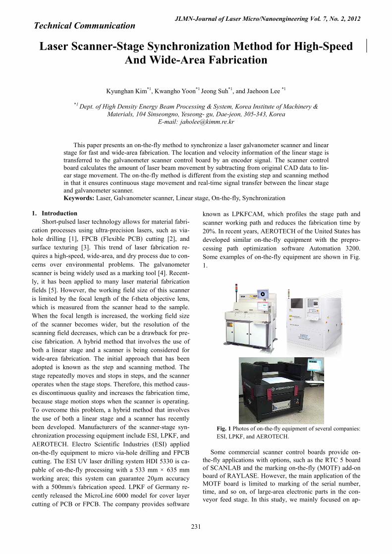
known as LPKFCAM, which profiles the stage path and scanner working path and reduces the fabrication time by 20%. In recent years, AEROTECH of the United States has developed similar on-the-fly equipment with the prepro-cessing path optimization software Automation 3200. Some examples of on-the-fly equipment are shown in Fig. 1.
Fig. 1 Photos of on-the-fly equipment of several companies: ESI, LPKF, and AEROTECH.
Some commercial scanner control boards provide on-
the-fly applications with options, such as the RTC 5 board of SCANLAB and the marking on-the-fly (MOTF) add-on board of RAYLASE. However, the main application of the MOTF board is limited to marking of the serial number, time, and so on, of large-area electronic parts in the con-veyor feed stage. In this study, we mainly focused on ap-
Technical Communication
JLMN-Journal of Laser Micro/Nanoengineering Vol. 7, No. 2, 2012
232
plication to FPCP cover layer cutting; the work can be summarized as follows:
(1) Stage path and velocity profiling software develop-ment for preprocessing
(2) On-the-fly control board development for laser fab-rication purposes
(3) On-the-fly system buildup with a linear stage (4) On-the-fly system validation by experiments
2. On-the-fly system configuration
2.1 Stage path/velocity profiling The on-the-fly control system is composed of stage
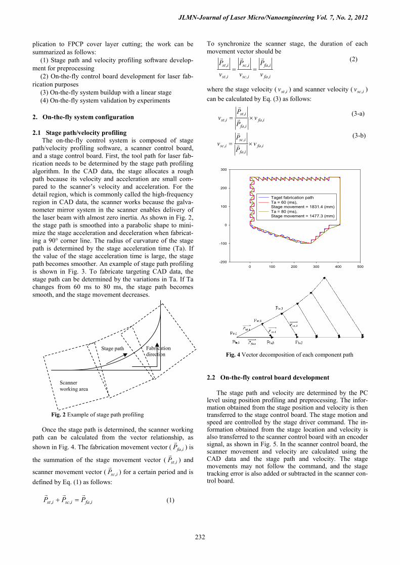
path/velocity profiling software, a scanner control board, and a stage control board. First, the tool path for laser fab-rication needs to be determined by the stage path profiling algorithm. In the CAD data, the stage allocates a rough path because its velocity and acceleration are small com-pared to the scanner’s velocity and acceleration. For the detail region, which is commonly called the high-frequency region in CAD data, the scanner works because the galva-nometer mirror system in the scanner enables delivery of the laser beam with almost zero inertia. As shown in Fig. 2, the stage path is smoothed into a parabolic shape to mini-mize the stage acceleration and deceleration when fabricat-ing a 90° corner line. The radius of curvature of the stage path is determined by the stage acceleration time (Ta). If the value of the stage acceleration time is large, the stage path becomes smoother. An example of stage path profiling is shown in Fig. 3. To fabricate targeting CAD data, the stage path can be determined by the variations in Ta. If Ta changes from 60 ms to 80 ms, the stage path becomes smooth, and the stage movement decreases.
Fig. 2 Example of stage path profiling Once the stage path is determined, the scanner working
path can be calculated from the vector relationship, as shown in Fig. 4. The fabrication movement vector ( ifaP ,
r) is
the summation of the stage movement vector ( istP ,r
) and
scanner movement vector ( iscP ,r
) for a certain period and is defined by Eq. (1) as follows:
ifaiscist PPP ,,,rrr
=+ (1)
To synchronize the scanner stage, the duration of each movement vector should be
(2)
where the stage velocity ( istv , ) and scanner velocity ( iscv , ) can be calculated by Eq. (3) as follows:
(3-a) (3-b)
Fig. 3 Change in stage path by variation in Ta value
Fig. 4 Vector decomposition of each component path
2.2 On-the-fly control board development
The stage path and velocity are determined by the PC level using position profiling and preprocessing. The infor-mation obtained from the stage position and velocity is then transferred to the stage control board. The stage motion and speed are controlled by the stage driver command. The in-formation obtained from the stage location and velocity is also transferred to the scanner control board with an encoder signal, as shown in Fig. 5. In the scanner control board, the scanner movement and velocity are calculated using the CAD data and the stage path and velocity. The stage movements may not follow the command, and the stage tracking error is also added or subtracted in the scanner con-trol board.
0 100 200 300 400 500-200
-100
0
100
200
300
Taget fabrication pathTa = 60 (ms), Stage movement = 1831.4 (mm)Ta = 80 (ms), Stage movement = 1477.3 (mm)
Fabrication direction
Stage path
Scanner working area
ifa
ifa
isc
isc
ist
ist
v
P
v
P
v
P
,
,
,
,
,
,rrr
==
ifaifa
istist v
P
Pv ,
,
,, ´= r
r
ifaifa
iscisc v
P
Pv ,
,
,, ´= r
r
JLMN-Journal of Laser Micro/Nanoengineering Vol. 7, No. 2, 2012
233
Fig. 5 On-the-fly control system layout
2.3 Comparison of on-the-fly method with step and scanning method
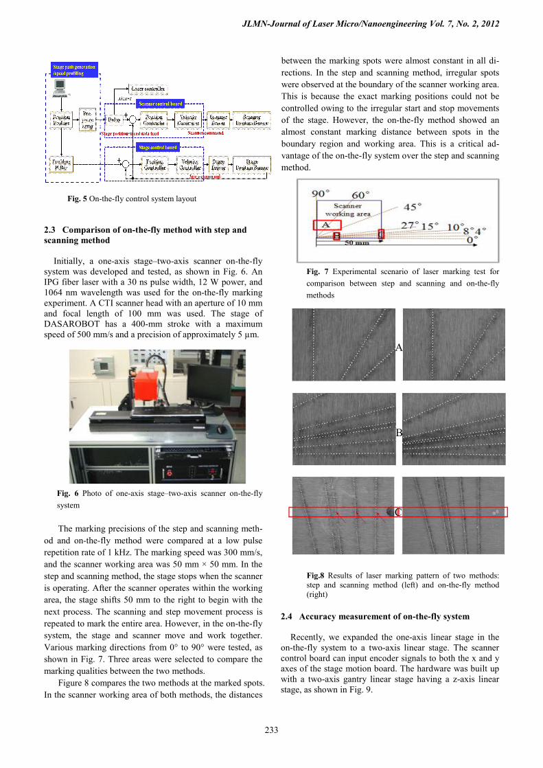
Initially, a one-axis stage–two-axis scanner on-the-fly
system was developed and tested, as shown in Fig. 6. An IPG fiber laser with a 30 ns pulse width, 12 W power, and 1064 nm wavelength was used for the on-the-fly marking experiment. A CTI scanner head with an aperture of 10 mm and focal length of 100 mm was used. The stage of DASAROBOT has a 400-mm stroke with a maximum speed of 500 mm/s and a precision of approximately 5 µm.
Fig. 6 Photo of one-axis stage–two-axis scanner on-the-fly system The marking precisions of the step and scanning meth-
od and on-the-fly method were compared at a low pulse repetition rate of 1 kHz. The marking speed was 300 mm/s, and the scanner working area was 50 mm × 50 mm. In the step and scanning method, the stage stops when the scanner is operating. After the scanner operates within the working area, the stage shifts 50 mm to the right to begin with the next process. The scanning and step movement process is repeated to mark the entire area. However, in the on-the-fly system, the stage and scanner move and work together. Various marking directions from 0° to 90° were tested, as shown in Fig. 7. Three areas were selected to compare the marking qualities between the two methods.
Figure 8 compares the two methods at the marked spots. In the scanner working area of both methods, the distances
between the marking spots were almost constant in all di-rections. In the step and scanning method, irregular spots were observed at the boundary of the scanner working area. This is because the exact marking positions could not be controlled owing to the irregular start and stop movements of the stage. However, the on-the-fly method showed an almost constant marking distance between spots in the boundary region and working area. This is a critical ad-vantage of the on-the-fly system over the step and scanning method.
Fig. 7 Experimental scenario of laser marking test for comparison between step and scanning and on-the-fly methods
Fig.8 Results of laser marking pattern of two methods: step and scanning method (left) and on-the-fly method (right)
2.4 Accuracy measurement of on-the-fly system
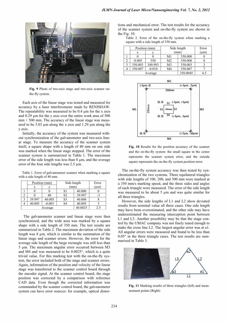
Recently, we expanded the one-axis linear stage in the
on-the-fly system to a two-axis linear stage. The scanner control board can input encoder signals to both the x and y axes of the stage motion board. The hardware was built up with a two-axis gantry linear stage having a z-axis linear stage, as shown in Fig. 9.
B
A
C
JLMN-Journal of Laser Micro/Nanoengineering Vol. 7, No. 2, 2012
234
Fig. 9 Photo of two-axis stage and two-axis scanner on-the-fly system.
Each axis of the linear stage was tested and measured for
accuracy by a laser interferometer made by RENISHAW. The repeatability was measured to be 0.4 µm for the x axis and 0.29 µm for the y axis over the entire work area of 500 mm × 500 mm. The accuracy of the linear stage was meas-ured to be 3.03 µm along the x axis and 1.29 µm along the y axis.
Initially, the accuracy of the system was measured with-out synchronization of the galvanometer and two-axis line-ar stage. To measure the accuracy of the scanner system itself, a square shape with a length of 40 mm on one side was marked when the linear stage stopped. The error of the scanner system is summarized in Table 1. The maximum error of the side length was less than 8 µm, and the average error of the four side lengths was 2.5 µm.
Table 1. Error of galvanometer scanner when marking a square
with a side length of 40 mm.
The galvanometer scanner and linear stage were then
synchronized, and the wide area was marked by a square shape with a side length of 350 mm. The test results are summarized in Table 2. The maximum deviation of the side length was 8 µm, which is similar to the summation of the linear stage and scanner errors. However, the error for the average side length of the large rectangle was still less than 5 µm. The maximum angular error occurred between M3 and M4 and was measured to be 0.0025°, which is a quite trivial value. For this marking test with the on-the-fly sys-tem, the error included both of the stage and scanner errors. Again, information of the position and velocity of the linear stage was transferred to the scanner control board through the encoder signal. At the scanner control board, the stage position was corrected by a comparison with reference CAD data. Even though the corrected information was commanded by the scanner control board, the galvanometer system can have error sources: for example, optical distor-
tions and mechanical error. The test results for the accuracy of the scanner system and on-the-fly system are shown in the Fig. 10.
Table 2. Error of the on-the-fly system when marking a square with a side length of 350 mm.
Fig. 10 Results for the position accuracy of the scanner and the on-the-fly system: the small square in the center represents the scanner system error, and the outside square represents the on-the-fly system position error.
The on-the-fly system accuracy was then tested by syn-
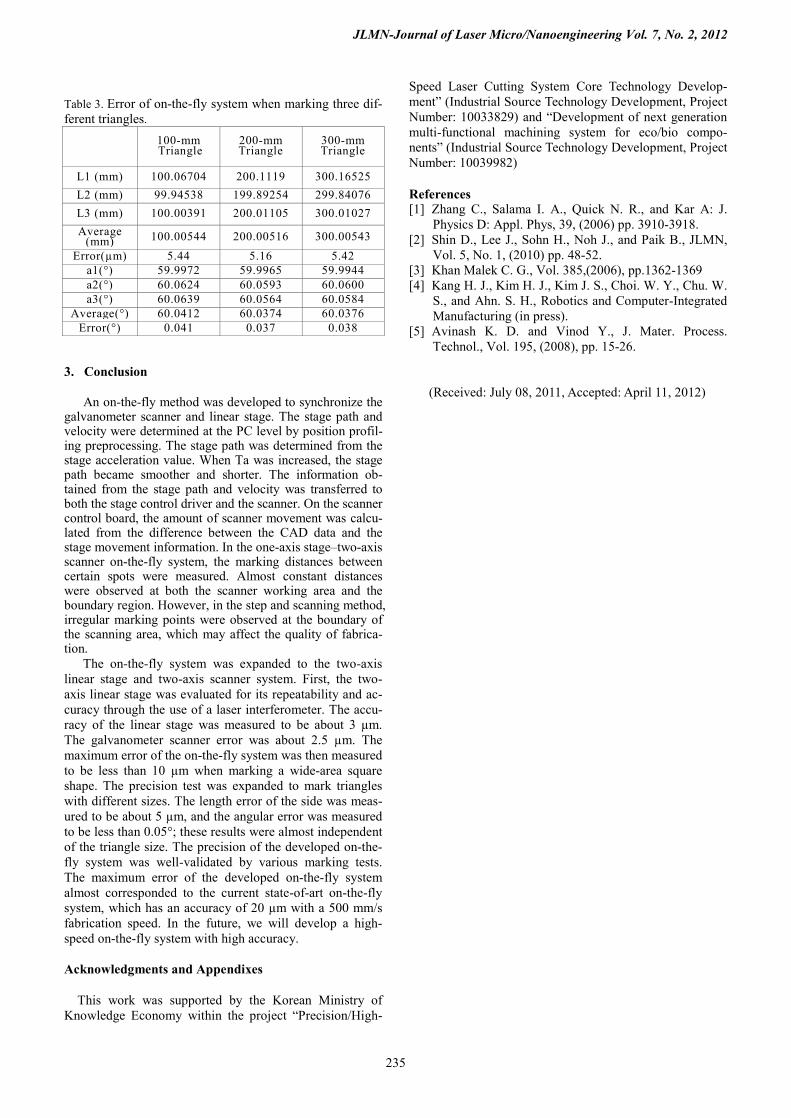
chronization of the two systems. Three equilateral triangles with side lengths of 100, 200, and 300 mm were marked at a 350 mm/s marking speed, and the three sides and angles of each triangle were measured. The error of the side length was measured to be about 5 µm and was quite similar for all three triangles.
However, the side lengths of L1 and L2 show deviated results from nominal value all three cases. One side length may have been overestimated, and the other side may have underestimated the measuring interception point between L1 and L3. Another possibility may be that the stage con-trol by the UMAC company was not finely tuned enough to make the cross line L2. The largest angular error was at a1. All angular errors were measured and found to be less than 0.05° in the three triangle cases. The test results are sum-marized in Table 3.
Fig. 11 Marking results of three triangles (left) and meas-urement points (Right)
Position (mm) Side length (mm)
Error (µm) x y
1 0 0 S1 40.000 0 2 0 40 S2 39.997 -3 3 39.997 40.005 S3 40.008 8 4 40.005 -0.003 S4 40.005 5
Average 40.0025 2.5
Position (mm) Side length (mm)
Error (µm) x y
1 0 0 M1 350.000 0 2 -0.005 350 M2 350.008 8 3 350.003 349.993 M3 350.003 3 4 350.007 -0.010 M4 350.007 7
Average 350.0045 4.5
JLMN-Journal of Laser Micro/Nanoengineering Vol. 7, No. 2, 2012
235
Table 3. Error of on-the-fly system when marking three dif-ferent triangles.
100-mm Triangle
200-mm Triangle
300-mm Triangle
L1 (mm) 100.06704 200.1119 300.16525 L2 (mm) 99.94538 199.89254 299.84076 L3 (mm) 100.00391 200.01105 300.01027 Average
(mm) 100.00544 200.00516 300.00543 Error(µm) 5.44 5.16 5.42
a1(°) 59.9972 59.9965 59.9944 a2(°) 60.0624 60.0593 60.0600 a3(°) 60.0639 60.0564 60.0584
Average(°) 60.0412 60.0374 60.0376 Error(°) 0.041 0.037 0.038
3. Conclusion
An on-the-fly method was developed to synchronize the galvanometer scanner and linear stage. The stage path and velocity were determined at the PC level by position profil-ing preprocessing. The stage path was determined from the stage acceleration value. When Ta was increased, the stage path became smoother and shorter. The information ob-tained from the stage path and velocity was transferred to both the stage control driver and the scanner. On the scanner control board, the amount of scanner movement was calcu-lated from the difference between the CAD data and the stage movement information. In the one-axis stage–two-axis scanner on-the-fly system, the marking distances between certain spots were measured. Almost constant distances were observed at both the scanner working area and the boundary region. However, in the step and scanning method, irregular marking points were observed at the boundary of the scanning area, which may affect the quality of fabrica-tion.
The on-the-fly system was expanded to the two-axis linear stage and two-axis scanner system. First, the two-axis linear stage was evaluated for its repeatability and ac-curacy through the use of a laser interferometer. The accu-racy of the linear stage was measured to be about 3 µm. The galvanometer scanner error was about 2.5 µm. The maximum error of the on-the-fly system was then measured to be less than 10 µm when marking a wide-area square shape. The precision test was expanded to mark triangles with different sizes. The length error of the side was meas-ured to be about 5 µm, and the angular error was measured to be less than 0.05°; these results were almost independent of the triangle size. The precision of the developed on-the-fly system was well-validated by various marking tests. The maximum error of the developed on-the-fly system almost corresponded to the current state-of-art on-the-fly system, which has an accuracy of 20 µm with a 500 mm/s fabrication speed. In the future, we will develop a high-speed on-the-fly system with high accuracy.
Acknowledgments and Appendixes
This work was supported by the Korean Ministry of Knowledge Economy within the project “Precision/High-
Speed Laser Cutting System Core Technology Develop-ment” (Industrial Source Technology Development, Project Number: 10033829) and “Development of next generation multi-functional machining system for eco/bio compo-nents” (Industrial Source Technology Development, Project Number: 10039982)
References [1] Zhang C., Salama I. A., Quick N. R., and Kar A: J.
Physics D: Appl. Phys, 39, (2006) pp. 3910-3918. [2] Shin D., Lee J., Sohn H., Noh J., and Paik B., JLMN,
Vol. 5, No. 1, (2010) pp. 48-52. [3] Khan Malek C. G., Vol. 385,(2006), pp.1362-1369 [4] Kang H. J., Kim H. J., Kim J. S., Choi. W. Y., Chu. W.
S., and Ahn. S. H., Robotics and Computer-Integrated Manufacturing (in press).
[5] Avinash K. D. and Vinod Y., J. Mater. Process. Technol., Vol. 195, (2008), pp. 15-26.
(Received: July 08, 2011, Accepted: April 11, 2012)