laser processing for the fabrication of mems devices · mems axial-flow turbine & generator for...
TRANSCRIPT
AILU Workshop, 22 September 2009 1
Laser Processing for theFabrication of MEMS Devices
Andrew S. Holmes
Optical & Semiconductor Devices Group Department of Electrical & Electronic Engineering
Imperial College, London SW7 2AZ, UK
AILU Workshop, 22 September 2009 2
Outline
• Motivation
• 3D and large area laser micromachining
• Laser transfer processes for MEMS
• Conclusions

AILU Workshop, 22 September 2009 3
Laser Processing for MEMS/Microsystems
MEMS (MicroElectroMechanical Systems) field traditionally dominated by silicon & silicon-related materials and processes
Car crash bag accelerometer [Ford]
Laser processing allows:
• Expansion of materials base:- Polymers- Biomaterials- Hard materials e.g. refractory metals, diamond, …- Functional materials e.g. piezoceramics, shape memory alloys
• Enhancement of 3D capabilities- 3D (i.e. not just prismatic) structures on planar substrates- Processing of non-planar surfaces e.g. for trimming
• New options for manipulation / assembly / joining of parts

AILU Workshop, 22 September 2009 4
Laser Machining for MEMS/Microsystems
Dielectrophoretic conveyer [Univ. Wales / Genera Technol. Ltd / Exitech Ltd, R Pethig et al, 1998]
Lab-on-chip technologyTypically glass/polymer substrate with channels and/or metal electrodes and/or functional layers• Laser can process all layers
Inkjet printer nozzle drillingLaser processing allows:• Tighter control over and greater
flexibility in sidewall profiles• Finer nozzle pitch; better finish• Multi-level machining for e.g.
reservoirsInk jet nozzles with reservoir [Exitech Ltd, N Rizvi et al, ca 2000]

AILU Workshop, 22 September 2009 5
Laser Machining for MEMS/Microsystems
RF MEMSDielectric substrates offer low loss, but are difficult to machine
• Laser attractive option for via drilling and singulation
RF switch arrays on glass for adaptive antennas[Thales TRT/Exitech Ltd, T Dean et al, 2004]
MEMS sensors/actuators
• Patterning of “tough” (to process) materials
• Patterning of thin films on devices/wafers with extreme topography Quartz MEMS accelerometers with laser machined
gold metallisation [Thales Avionics/Exitech Ltd, O Lefort et al, 2004]
AILU Workshop, 22 September 2009 6
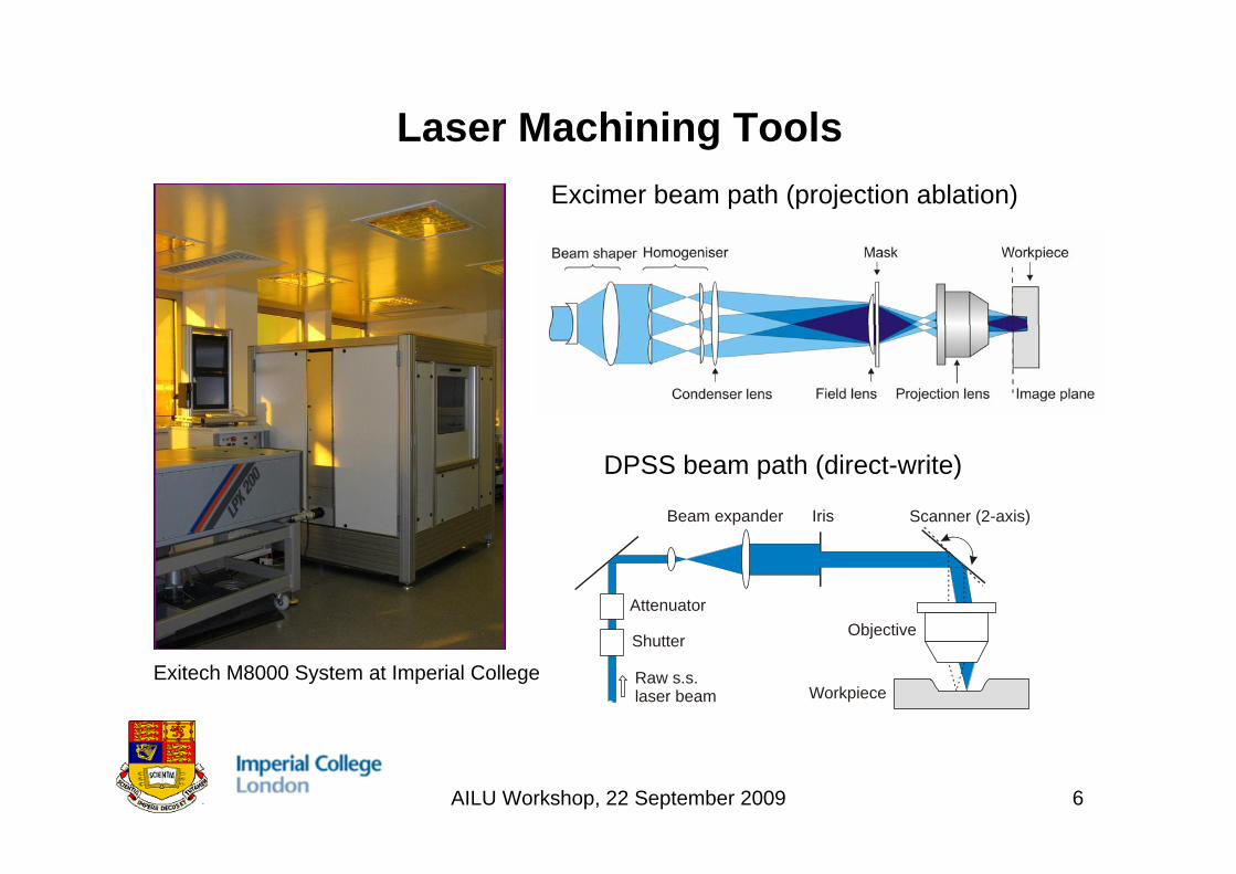
Laser Machining Tools
Workpiece
Beam expander
Raw s.s. laser beam
Iris Scanner (2-axis)
ObjectiveShutter
Attenuator
Exitech M8000 System at Imperial College
Excimer beam path (projection ablation)
DPSS beam path (direct-write)
AILU Workshop, 22 September 2009 7
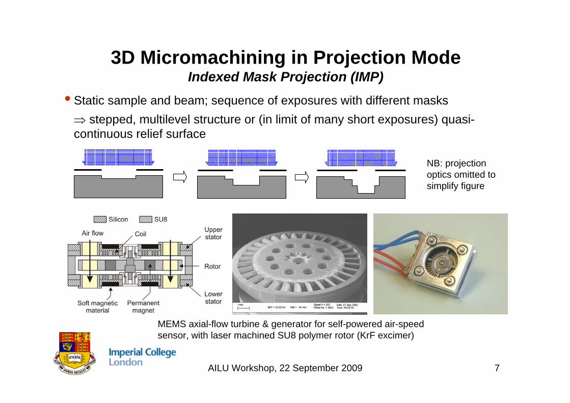
3D Micromachining in Projection ModeIndexed Mask Projection (IMP)
• Static sample and beam; sequence of exposures with different masks⇒ stepped, multilevel structure or (in limit of many short exposures) quasi-continuous relief surface
MEMS axial-flow turbine & generator for self-powered air-speed sensor, with laser machined SU8 polymer rotor (KrF excimer)
NB: projection optics omitted to simplify figure

AILU Workshop, 22 September 2009 8
3D Micromachining in Projection ModeHalf-tone Machining
w
p
h
• Pixellated binary mask with pixels sized below resolution of projection optics
• Mask behaves as (spatially) variable attenuator with local transmission:
• Attractive for small-area applications because less costly in terms of mask real estate
• Ultimately less efficient than IMP because fluence levels very close to threshold are unusable in practice (debris issues)
T = (wh/p2)2
Polycarbonate micro-optical parts formed by half-tone ablation (KrF excimer)
• Potential MEMS applications in microfluidics & microchemistry e.g. channels, mixers, filters and micro-optics

AILU Workshop, 22 September 2009 9
Large Area MachiningSynchronised Image Scanning (SIS)
SIS microlens array [Exitech Ltd]
• Similar to IMP but with indexed workpiece; suitable for large area arrays • Letter box beam illuminates array of mask apertures on fixed pitch s;
workpiece translated by distance s after every pulse
• Each exposure site sees all apertures in turn• Different apertures illuminated by different
parts of beam- Reduces projection lens telecentricity errors- Reduces distortions caused by non-uniform illumination

AILU Workshop, 22 September 2009 10
SIS with Half-tone• SIS with normal binary masks leaves unwanted stepping in the final surface• This can be virtually eliminated by incorporating half-tone into the SIS mask
array, giving surfaces with exceptionally low roughness:
• Central region of each microlenshas line roughness Ra <10 nm
50 μm
Microlens array formed in polycarbonate by HT-SIS
• Similar results can be achieved by laser polishing after binary mask SIS, but this requires a second process step

AILU Workshop, 22 September 2009 11
Mask Design Tools
CAD/CAM Mask design
Mask projection- static
Mask projection - dynamic
Parts
Typical laser microfabrication route using Excimer laser:
Iteration
• Simulation can assist in mask design, reducing requirement for iterative process that includes prototyping
• Useful for structures that are deep (compared to focal depth) and/or contain steeply inclined surfaces e.g. turbine rotor shown earlier
Simulation
AILU Workshop, 22 September 2009 12
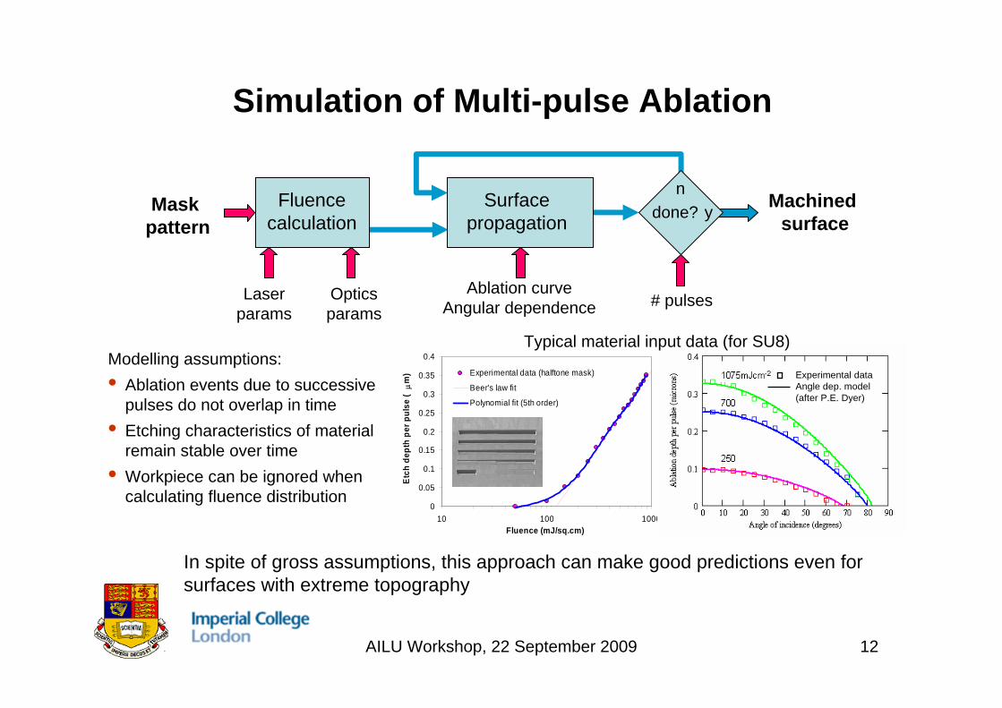
Simulation of Multi-pulse Ablation
Fluence calculation
Laserparams
Optics params
Mask pattern
Surface propagation
Machined surface
# pulses Ablation curve
Angular dependence
done?n
y
0
0.05
0.1
0.15
0.2
0.25
0.3
0.35
0.4
10 100 1000Fluence (mJ/sq.cm)
Etch
dep
th p
er p
ulse
(μ
m) Experimental data (halftone mask)
Beer's law fit
Polynomial fit (5th order)
Modelling assumptions:• Ablation events due to successive
pulses do not overlap in time• Etching characteristics of material
remain stable over time• Workpiece can be ignored when
calculating fluence distribution
In spite of gross assumptions, this approach can make good predictions even for surfaces with extreme topography
Experimental dataAngle dep. model(after P.E. Dyer)
Typical material input data (for SU8)
AILU Workshop, 22 September 2009 13
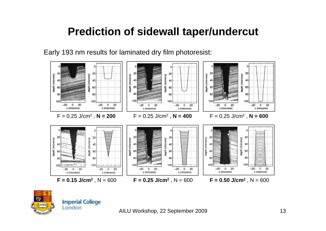
Prediction of sidewall taper/undercut
Early 193 nm results for laminated dry film photoresist:
F = 0.25 J/cm2 , N = 200 F = 0.25 J/cm2 , N = 400 F = 0.25 J/cm2 , N = 600
F = 0.15 J/cm2 , N = 600 F = 0.25 J/cm2 , N = 600 F = 0.50 J/cm2 , N = 600

AILU Workshop, 22 September 2009 14
Plots compare experimental profiles with simulations using (a) angular dependence model normally assumed in literature (dashed line) and (b) empirical angle-dependent etch function (solid line)Use of empirical angular dependence significantly improves simulation accuracy for deeper structures, with good predictions even in regions with extreme gradient Improved angular dependence model, recently proposed by P.E. Dyer (and pending publication), will reduce the need for empirical data
Simulation of deep Half-tone Ablation

AILU Workshop, 22 September 2009 15
Laser Transfer Processes• Processes such as LIFT (Laser Induced Forward Transfer) and MAPLE (Matrix
Assisted Pulsed Laser Evaporation) are well-established methods for selective transfer of materials from one wafer to another:
[Potomac Photonics Inc / NRL, S A Mathews et al, 2000]Direct-write 2-level spiral inductor on polyimide
• A similar approach may be used for assembly of MEMS devices from parts fabricated on separate wafers. This can be useful where a fully monolithic approach is difficult or impossible due to yield or process compatibility issues
MAPLE-DW process

AILU Workshop, 22 September 2009 16
Laser Transfer of Parts
Pulsed UV radiation Pulsed UV radiationRelease layer
Carrier
Target
• Confined ablation of release layer through (UV-transparent) carrier• Expanding ablation products impart momentum to released part• Several applications to date
- Assembly of hybrid MEMS – first demonstration (Imperial College, 1998)- Transfer of metal/solder bumps for flip-chip assembly (Imperial College/Celestica)- Release of IC dies from “blue tape” (Philips/Univ. Twente)- Assembly of electronic circuits (NRL/Princeton Univ./ Catholic Univ. of America)
AILU Workshop, 22 September 2009 17
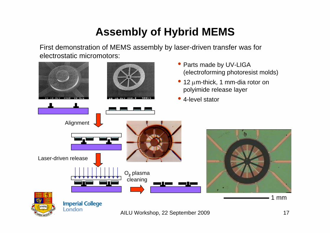
Assembly of Hybrid MEMS
Alignment
Laser-driven release
O2 plasma cleaning
• Parts made by UV-LIGA (electroforming photoresist molds)
• 12 μm-thick, 1 mm-dia rotor on polyimide release layer
• 4-level stator
1 mm
First demonstration of MEMS assembly by laser-driven transfer was for electrostatic micromotors:
AILU Workshop, 22 September 2009 18
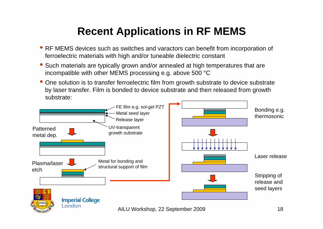
Recent Applications in RF MEMS• RF MEMS devices such as switches and varactors can benefit from incorporation of
ferroelectric materials with high and/or tuneable dielectric constant• Such materials are typically grown and/or annealed at high temperatures that are
incompatible with other MEMS processing e.g. above 500 °C• One solution is to transfer ferroelectric film from growth substrate to device substrate
by laser transfer. Film is bonded to device substrate and then released from growth substrate:
FE film e.g. sol-gel PZTMetal seed layerRelease layer
UV-transparent growth substrate
Metal for bonding and structural support of film
Bonding e.g. thermosonic
Laser release
Stripping of release and seed layers
Patterned metal dep.
Plasma/laser etch

AILU Workshop, 22 September 2009 19
Laser Transfer of PZT – First Results
This work is a collaboration with Cranfield University
Silica ITOTi/Pt
PZT (0.5 μm)
Ni/Au
TS bonding +laser release
SiliconTransferred PZT is damage-free except near edges
• PZT/Ti/Pt/ITO surrounding pad to be transferred is removed by front side ablation• PZT can be transferred by single KrF laser pulse in fluence range 120-180 mJ/cm2
• Bond metal provides structural support during laser transfer and prevents mechanical damage to film (in contrast, films transferred without bond metal tend to fracture)
• Delamination can occur at the PZT/Ti interface rather than silica/ITO; unexpected but not necessarily undesirable (if reproducible)

AILU Workshop, 22 September 2009 20
Laser transfer of PZT – Target DeviceCurrently fabricating “zipping” varactors with sputtered silica dielectric:
0
50
100
150
200
250
300
350
0 10 20 30 40 50
Bias Voltage [V]
Cap
acita
nce
C [f
F]
TS bond &Laser release
TS bond &Laser release
Possible scheme for integrating ferroelectric layers by laser transfer:

AILU Workshop, 22 September 2009 21
Summary• Many potential applications for laser processing in MEMS manufacture,
of which only two discussed here: - 3D machining in projection mode - Laser transfer of parts/layers
• Several approaches available for 3D structuring, all of which can achieve good profile accuracy with correct mask & process design
• Half-tone masking attractive for small-area applications because less costly in terms of mask area; other methods preferred for large areas
• Laser transfer can overcome yield and process incompatibility issues that may preclude monolithic processing. Currently we are developing this approach for integration of functional materials into RF MEMS devices
AILU Workshop, 22 September 2009 22
Acknowledgements
This work was funded by the UK Engineering & Physical Sciences Research Council (EPSRC)
Laser micromachining results were obtained using laser facilities kindly provided by Exitech Ltd / Oerlikon Optics UK Ltd
James Pedder (now with M-Solv Ltd) carried out most of the laser machining work as part of an Industrial CASE Studentship with Imperial College and Exitech Ltd
Bob Hergert conducted the recent PZT laser transfer trials using material provided by Cranfield University