laser induced changes on a-ga 50 se 50 thin...
TRANSCRIPT
This content has been downloaded from IOPscience. Please scroll down to see the full text.
Download details:
IP Address: 132.203.227.62
This content was downloaded on 08/07/2014 at 19:35
Please note that terms and conditions apply.
Laser induced changes on a-Ga50Se50 thin films
View the table of contents for this issue, or go to the journal homepage for more
2009 J. Phys. D: Appl. Phys. 42 185404
(http://iopscience.iop.org/0022-3727/42/18/185404)
Home Search Collections Journals About Contact us My IOPscience
IOP PUBLISHING JOURNAL OF PHYSICS D: APPLIED PHYSICS
J. Phys. D: Appl. Phys. 42 (2009) 185404 (7pp) doi:10.1088/0022-3727/42/18/185404
Laser induced changes on a-Ga50Se50 thinfilmsS K Tripathi1, Shikha Gupta, F I Mustafa, N Goyal and G S S Saini
Department of Physics, Panjab University, Chandigarh 160 014, India
E-mail: [email protected] and surya [email protected]
Received 19 December 2008, in final form 9 July 2009Published 28 August 2009Online at stacks.iop.org/JPhysD/42/185404
AbstractThis paper reports on the laser induced changes on the optical properties of a-Ga50Se50 thinfilms prepared by the thermal evaporation technique under vacuum. Thin film samples, on aglass substrate, were exposed to laser light of wavelength λ = 532 nm for different exposuretimes, tE (tE = 0, 500, 1500 and 3000 s). Optical parameters such as refractive index,absorption coefficient, optical gap, extinction coefficient, real and imaginary dielectricconstants, dielectric loss, optical conductivity of as-deposited thin film and their laser inducedchanges were studied at three different times of exposure. The mechanism of optical absorptionfollows the rule of the indirect allowed transition model proposed by Tauc and the optical bandgap is calculated by Tauc’s extrapolation. It is seen that after laser irradiation there is a shift ofthe optical absorption edge to larger photon energy. The value of the absorption coefficient ofthe GaSe thin film decreases on exposing the film to laser irradiation. A microscopic model inwhich heteropolar bonds are broken by absorption of high energy photons and new homopolarbonds are formed simultaneously has been used to describe the effect.
1. Introduction
Interest in the optical properties of chalcogenide glasses hasrecently increased as they are very promising materials foruse in optoelectronic applications [1]. These glasses are veryinteresting materials for infrared optics. They have a largerange of transparency (∼0.6–30 µm) and good mechanicaland chemical properties, such as hardness, adhesion, lowinternal stress and water resistance. The low characteristicvibrational frequencies of the chalcogenide bonds allow themto transmit far out into the infrared [2]. These glasses showa variety of photo-stimulated phenomena when exposed tolight or other radiations [3–7]. When these glasses areirradiated with high energy particles or light, bond breakingand bond rearrangement can take place, which result in thechange in the local structure of the glassy materials. Theseinclude subtle effects such as shifts in the absorption edge(photo-bleaching and photo-darkening), and more substantialatomic and molecular reconfiguration such as photo-inducedrefractive index changes and photo-doping effects [8, 9]. Ingeneral, these phenomena are associated with changes inthe optical constants [10, 11] and absorption edge shift [12].These light-induced changes are favoured in chalcogenide
1 Author to whom any correspondence should be addressed.
glasses due to their structural flexibility (low coordination ofchalcogens) and also due to their high-lying lone-pair p statesin their valence bands. In the last few decades, many potentialapplications based on light-induced effects have been explored,for example, in the fields of sub-micrometre, photo-resists,optical memories, diffraction elements, optical light-guideand optoelectronic elements and devices. Semiconductoroptoelectronic devices can be operated under conditions ofthe action of different kinds of high energy radiation. Theduration, intensity and energy of such radiations influencesdifferently the parameters of these devices. Therefore, anestablishment of the regularities in the changes in the devicecharacteristics affected by radiation can be used for adjustmentof their operating conditions.
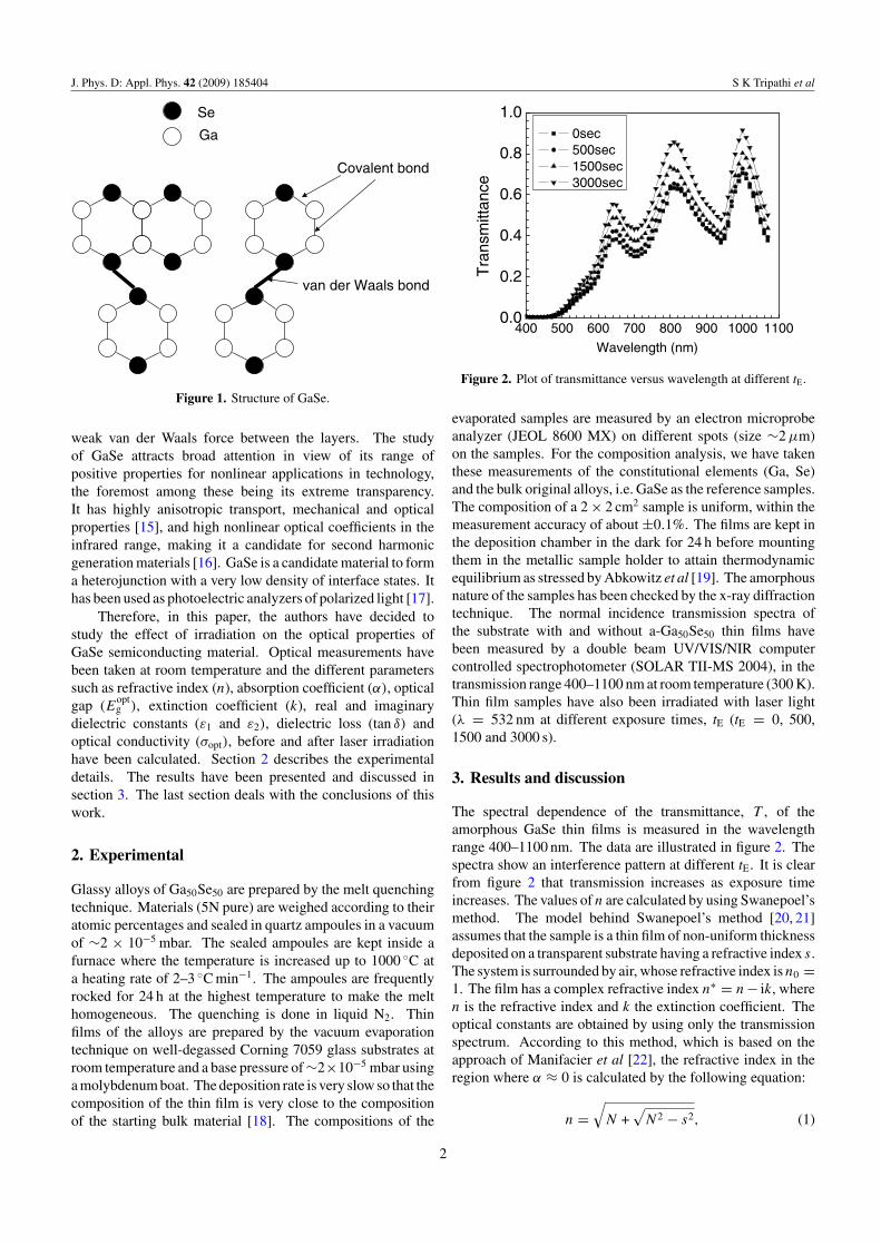
GaSe is a member of the III–VI layered semiconductorfamily that has been a subject of several investigations in recentyears. Figure 1 shows the layer structure of GaSe which ischaracterized by the covalent bond and is restricted in twodimensions in the plane of the layer and with van der Waalsforces in the third dimension. These films have typicalcharacteristics of semiconductor layers such as (i) a lowdensity of dangling bonds on the surface because of thealmost complete chemical bonds within the layer [13], (ii)intercalation [14] and (iii) mechanical weakness due to the
0022-3727/09/185404+07$30.00 1 © 2009 IOP Publishing Ltd Printed in the UK
J. Phys. D: Appl. Phys. 42 (2009) 185404 S K Tripathi et al
Ga
van der Waals bond
Covalent bond
Se
Figure 1. Structure of GaSe.
weak van der Waals force between the layers. The studyof GaSe attracts broad attention in view of its range ofpositive properties for nonlinear applications in technology,the foremost among these being its extreme transparency.It has highly anisotropic transport, mechanical and opticalproperties [15], and high nonlinear optical coefficients in theinfrared range, making it a candidate for second harmonicgeneration materials [16]. GaSe is a candidate material to forma heterojunction with a very low density of interface states. Ithas been used as photoelectric analyzers of polarized light [17].
Therefore, in this paper, the authors have decided tostudy the effect of irradiation on the optical properties ofGaSe semiconducting material. Optical measurements havebeen taken at room temperature and the different parameterssuch as refractive index (n), absorption coefficient (α), opticalgap (Eopt
g ), extinction coefficient (k), real and imaginarydielectric constants (ε1 and ε2), dielectric loss (tan δ) andoptical conductivity (σopt), before and after laser irradiationhave been calculated. Section 2 describes the experimentaldetails. The results have been presented and discussed insection 3. The last section deals with the conclusions of thiswork.
2. Experimental
Glassy alloys of Ga50Se50 are prepared by the melt quenchingtechnique. Materials (5N pure) are weighed according to theiratomic percentages and sealed in quartz ampoules in a vacuumof ∼2 × 10⁻⁵ mbar. The sealed ampoules are kept inside afurnace where the temperature is increased up to 1000 ◦C ata heating rate of 2–3 ◦C min−1. The ampoules are frequentlyrocked for 24 h at the highest temperature to make the melthomogeneous. The quenching is done in liquid N2. Thinfilms of the alloys are prepared by the vacuum evaporationtechnique on well-degassed Corning 7059 glass substrates atroom temperature and a base pressure of ∼2×10⁻⁵ mbar usinga molybdenum boat. The deposition rate is very slow so that thecomposition of the thin film is very close to the compositionof the starting bulk material [18]. The compositions of the
400 500 600 700 800 900 1000 11000.0
0.2
0.4
0.6
0.8
1.0
Tra
nsm
ittan
ce
Wavelength (nm)
0sec 500sec 1500sec 3000sec
Figure 2. Plot of transmittance versus wavelength at different tE.
evaporated samples are measured by an electron microprobeanalyzer (JEOL 8600 MX) on different spots (size ∼2 µm)on the samples. For the composition analysis, we have takenthese measurements of the constitutional elements (Ga, Se)and the bulk original alloys, i.e. GaSe as the reference samples.The composition of a 2 × 2 cm2 sample is uniform, within themeasurement accuracy of about ±0.1%. The films are kept inthe deposition chamber in the dark for 24 h before mountingthem in the metallic sample holder to attain thermodynamicequilibrium as stressed by Abkowitz et al [19]. The amorphousnature of the samples has been checked by the x-ray diffractiontechnique. The normal incidence transmission spectra ofthe substrate with and without a-Ga50Se50 thin films havebeen measured by a double beam UV/VIS/NIR computercontrolled spectrophotometer (SOLAR TII-MS 2004), in thetransmission range 400–1100 nm at room temperature (300 K).Thin film samples have also been irradiated with laser light(λ = 532 nm at different exposure times, tE (tE = 0, 500,1500 and 3000 s).
3. Results and discussion
The spectral dependence of the transmittance, T , of theamorphous GaSe thin films is measured in the wavelengthrange 400–1100 nm. The data are illustrated in figure 2. Thespectra show an interference pattern at different tE. It is clearfrom figure 2 that transmission increases as exposure timeincreases. The values of n are calculated by using Swanepoel’smethod. The model behind Swanepoel’s method [20, 21]assumes that the sample is a thin film of non-uniform thicknessdeposited on a transparent substrate having a refractive index s.The system is surrounded by air, whose refractive index is n0 =1. The film has a complex refractive index n∗ = n− ik, wheren is the refractive index and k the extinction coefficient. Theoptical constants are obtained by using only the transmissionspectrum. According to this method, which is based on theapproach of Manifacier et al [22], the refractive index in theregion where α ≈ 0 is calculated by the following equation:
n =√
N +√
N2 − s2, (1)
2
J. Phys. D: Appl. Phys. 42 (2009) 185404 S K Tripathi et al
where
N = 2sTmax − Tmin
TmaxTmin+
s2 + 1
2, (2)
where Tmax and Tmin are the envelope values at the wavelengthsin which the upper and lower envelopes and the experimentaltransmission spectrum are tangent, respectively, as shown infigure 2 and s is the refractive index of the substrate. Theaccuracy to which λ can be measured is ±1 nm. The maximumabsolute accuracy of Tmax and Tmin is ±0.001. The values of n
are calculated using equation (1) at wavelengths correspondingto the tangent points. If n1 and n2 are the refractive indices attwo adjacent tangent points at λ1 and λ2, then according to thebasic equation for interference fringes
2nd = mλ, (3)
where d is the film thickness and m is an order number. Thethickness is given by
d = λ1λ2
2 (λ1n2 − λ2n1). (4)
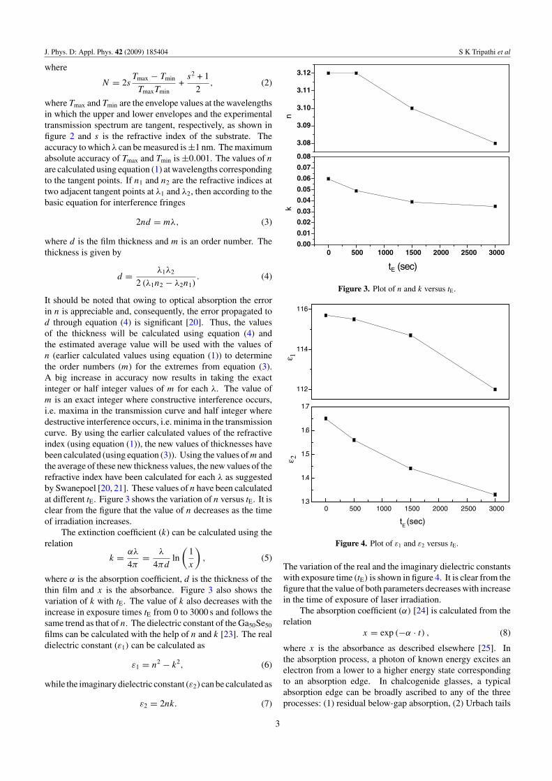
It should be noted that owing to optical absorption the errorin n is appreciable and, consequently, the error propagated tod through equation (4) is significant [20]. Thus, the valuesof the thickness will be calculated using equation (4) andthe estimated average value will be used with the values ofn (earlier calculated values using equation (1)) to determinethe order numbers (m) for the extremes from equation (3).A big increase in accuracy now results in taking the exactinteger or half integer values of m for each λ. The value ofm is an exact integer where constructive interference occurs,i.e. maxima in the transmission curve and half integer wheredestructive interference occurs, i.e. minima in the transmissioncurve. By using the earlier calculated values of the refractiveindex (using equation (1)), the new values of thicknesses havebeen calculated (using equation (3)). Using the values of m andthe average of these new thickness values, the new values of therefractive index have been calculated for each λ as suggestedby Swanepoel [20, 21]. These values of n have been calculatedat different tE. Figure 3 shows the variation of n versus tE. It isclear from the figure that the value of n decreases as the timeof irradiation increases.
The extinction coefficient (k) can be calculated using therelation
k = αλ
4π= λ
4πdln
(1
x
), (5)
where α is the absorption coefficient, d is the thickness of thethin film and x is the absorbance. Figure 3 also shows thevariation of k with tE. The value of k also decreases with theincrease in exposure times tE from 0 to 3000 s and follows thesame trend as that of n. The dielectric constant of the Ga50Se50
films can be calculated with the help of n and k [23]. The realdielectric constant (ε1) can be calculated as
ε1 = n2 − k2, (6)
while the imaginary dielectric constant (ε2) can be calculated as
ε2 = 2nk. (7)
0 500 1000 1500 2000 2500 30000.00
0.01
0.02
0.03
0.04
0.05
0.06
0.07
0.08
3.08
3.09
3.10
3.11
3.12
k
tE (sec)
nFigure 3. Plot of n and k versus tE.
0 500 1000 1500 2000 2500 30001.3
1.4
1.5
1.6
1.7
11.2
11.4
11.6
2
tE (sec)
1ε
ε
Figure 4. Plot of ε1 and ε2 versus tE.
The variation of the real and the imaginary dielectric constantswith exposure time (tE) is shown in figure 4. It is clear from thefigure that the value of both parameters decreases with increasein the time of exposure of laser irradiation.
The absorption coefficient (α) [24] is calculated from therelation
x = exp (−α · t) , (8)
where x is the absorbance as described elsewhere [25]. Inthe absorption process, a photon of known energy excites anelectron from a lower to a higher energy state correspondingto an absorption edge. In chalcogenide glasses, a typicalabsorption edge can be broadly ascribed to any of the threeprocesses: (1) residual below-gap absorption, (2) Urbach tails
3
J. Phys. D: Appl. Phys. 42 (2009) 185404 S K Tripathi et al
1.2 1.4 1.6 1.8 2.0 2.2 2.4 2.60
50
100
150
200
250
300
350
400
450
500
1.2 1.6 2.0 2.4 2.80
2
4
6
8
10
12
×104
(cm
-1)
h (eV)
0 s 500 s 1500 s 3000 s
( h
)1/2 (
cm -
1 eV
) 1/2
0 s 500 s 1500 s 3000s
h (eV)
ν
ν
αν
α
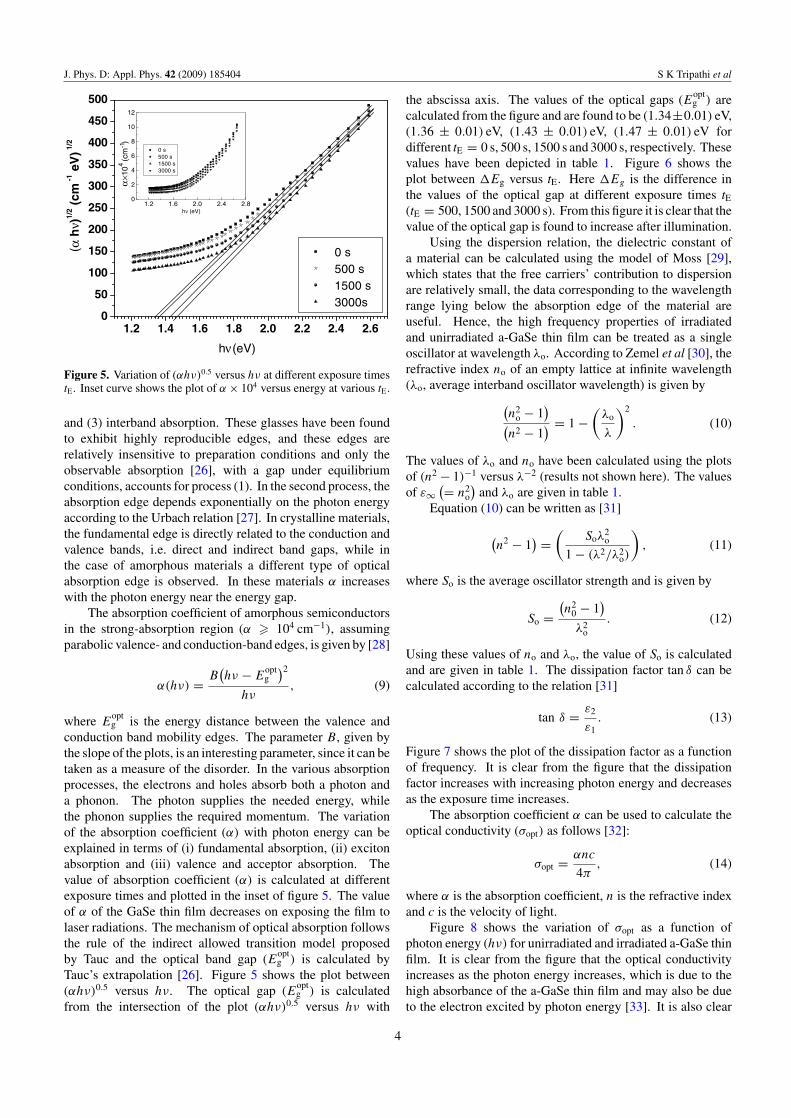
Figure 5. Variation of (αhν)0.5 versus hν at different exposure timestE. Inset curve shows the plot of α × 104 versus energy at various tE.
and (3) interband absorption. These glasses have been foundto exhibit highly reproducible edges, and these edges arerelatively insensitive to preparation conditions and only theobservable absorption [26], with a gap under equilibriumconditions, accounts for process (1). In the second process, theabsorption edge depends exponentially on the photon energyaccording to the Urbach relation [27]. In crystalline materials,the fundamental edge is directly related to the conduction andvalence bands, i.e. direct and indirect band gaps, while inthe case of amorphous materials a different type of opticalabsorption edge is observed. In these materials α increaseswith the photon energy near the energy gap.
The absorption coefficient of amorphous semiconductorsin the strong-absorption region (α � 104 cm−1), assumingparabolic valence- and conduction-band edges, is given by [28]
α(hν) = B(hν − E
optg
)2
hν, (9)
where Eoptg is the energy distance between the valence and
conduction band mobility edges. The parameter B, given bythe slope of the plots, is an interesting parameter, since it can betaken as a measure of the disorder. In the various absorptionprocesses, the electrons and holes absorb both a photon anda phonon. The photon supplies the needed energy, whilethe phonon supplies the required momentum. The variationof the absorption coefficient (α) with photon energy can beexplained in terms of (i) fundamental absorption, (ii) excitonabsorption and (iii) valence and acceptor absorption. Thevalue of absorption coefficient (α) is calculated at differentexposure times and plotted in the inset of figure 5. The valueof α of the GaSe thin film decreases on exposing the film tolaser radiations. The mechanism of optical absorption followsthe rule of the indirect allowed transition model proposedby Tauc and the optical band gap (Eopt
g ) is calculated byTauc’s extrapolation [26]. Figure 5 shows the plot between(αhν)0.5 versus hν. The optical gap (Eopt
g ) is calculatedfrom the intersection of the plot (αhν)0.5 versus hν with
the abscissa axis. The values of the optical gaps (Eoptg ) are
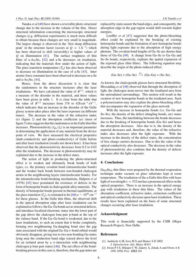
calculated from the figure and are found to be (1.34±0.01) eV,(1.36 ± 0.01) eV, (1.43 ± 0.01) eV, (1.47 ± 0.01) eV fordifferent tE = 0 s, 500 s, 1500 s and 3000 s, respectively. Thesevalues have been depicted in table 1. Figure 6 shows theplot between �Eg versus tE. Here �Eg is the difference inthe values of the optical gap at different exposure times tE(tE = 500, 1500 and 3000 s). From this figure it is clear that thevalue of the optical gap is found to increase after illumination.
Using the dispersion relation, the dielectric constant ofa material can be calculated using the model of Moss [29],which states that the free carriers’ contribution to dispersionare relatively small, the data corresponding to the wavelengthrange lying below the absorption edge of the material areuseful. Hence, the high frequency properties of irradiatedand unirradiated a-GaSe thin film can be treated as a singleoscillator at wavelength λo. According to Zemel et al [30], therefractive index no of an empty lattice at infinite wavelength(λo, average interband oscillator wavelength) is given by
(n2
o − 1)
(n2 − 1
) = 1 −(
λo
λ
)2
. (10)
The values of λo and no have been calculated using the plotsof (n2 − 1)−1 versus λ−2 (results not shown here). The valuesof ε∞
(= n2o
)and λo are given in table 1.
Equation (10) can be written as [31]
(n2 − 1
) =(
Soλ2o
1 − (λ2/λ2o)
), (11)
where So is the average oscillator strength and is given by
So =(n2
0 − 1)
λ2o
. (12)
Using these values of no and λo, the value of So is calculatedand are given in table 1. The dissipation factor tan δ can becalculated according to the relation [31]
tan δ = ε2
ε1. (13)
Figure 7 shows the plot of the dissipation factor as a functionof frequency. It is clear from the figure that the dissipationfactor increases with increasing photon energy and decreasesas the exposure time increases.
The absorption coefficient α can be used to calculate theoptical conductivity (σopt) as follows [32]:
σopt = αnc
4π, (14)
where α is the absorption coefficient, n is the refractive indexand c is the velocity of light.
Figure 8 shows the variation of σopt as a function ofphoton energy (hν) for unirradiated and irradiated a-GaSe thinfilm. It is clear from the figure that the optical conductivityincreases as the photon energy increases, which is due to thehigh absorbance of the a-GaSe thin film and may also be dueto the electron excited by photon energy [33]. It is also clear
4
J. Phys. D: Appl. Phys. 42 (2009) 185404 S K Tripathi et al
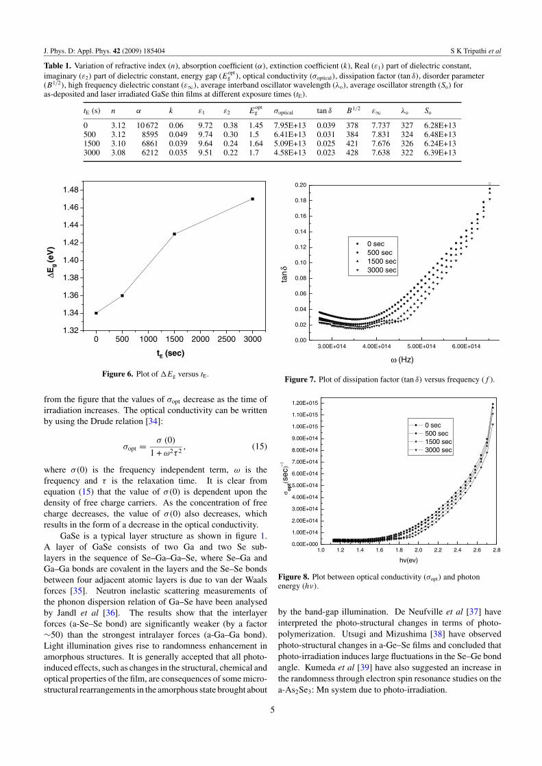
Table 1. Variation of refractive index (n), absorption coefficient (α), extinction coefficient (k), Real (ε1) part of dielectric constant,imaginary (ε2) part of dielectric constant, energy gap (Eopt
g ), optical conductivity (σoptical), dissipation factor (tan δ), disorder parameter(B1/2), high frequency dielectric constant (ε∞), average interband oscillator wavelength (λo), average oscillator strength (So) foras-deposited and laser irradiated GaSe thin films at different exposure times (tE).
tE (s) n α k ε1 ε2 Eoptg σoptical tan δ B1/2 ε∞ λo So
0 3.12 10 672 0.06 9.72 0.38 1.45 7.95E+13 0.039 378 7.737 327 6.28E+13500 3.12 8595 0.049 9.74 0.30 1.5 6.41E+13 0.031 384 7.831 324 6.48E+131500 3.10 6861 0.039 9.64 0.24 1.64 5.09E+13 0.025 421 7.676 326 6.24E+133000 3.08 6212 0.035 9.51 0.22 1.7 4.58E+13 0.023 428 7.638 322 6.39E+13
0 500 1000 1500 2000 2500 30001.32
1.34
1.36
1.38
1.40
1.42
1.44
1.46
1.48
g
tE (sec)
∆E (
eV)
Figure 6. Plot of �Eg versus tE.
from the figure that the values of σopt decrease as the time ofirradiation increases. The optical conductivity can be writtenby using the Drude relation [34]:
σopt = σ (0)
1 + ω2τ 2, (15)
where σ (0) is the frequency independent term, ω is thefrequency and τ is the relaxation time. It is clear fromequation (15) that the value of σ (0) is dependent upon thedensity of free charge carriers. As the concentration of freecharge decreases, the value of σ (0) also decreases, whichresults in the form of a decrease in the optical conductivity.
GaSe is a typical layer structure as shown in figure 1.A layer of GaSe consists of two Ga and two Se sub-layers in the sequence of Se–Ga–Ga–Se, where Se–Ga andGa–Ga bonds are covalent in the layers and the Se–Se bondsbetween four adjacent atomic layers is due to van der Waalsforces [35]. Neutron inelastic scattering measurements ofthe phonon dispersion relation of Ga–Se have been analysedby Jandl et al [36]. The results show that the interlayerforces (a-Se–Se bond) are significantly weaker (by a factor∼50) than the strongest intralayer forces (a-Ga–Ga bond).Light illumination gives rise to randomness enhancement inamorphous structures. It is generally accepted that all photo-induced effects, such as changes in the structural, chemical andoptical properties of the film, are consequences of some micro-structural rearrangements in the amorphous state brought about
3.00E+014 4.00E+014 5.00E+014 6.00E+0140.00
0.02
0.04
0.06
0.08
0.10
0.12
0.14
0.16
0.18
0.20
0 sec 500 sec 1500 sec 3000 sec
tan
δ
(Hz)ω
Figure 7. Plot of dissipation factor (tan δ) versus frequency (f ).
1.0 1.2 1.4 1.6 1.8 2.0 2.2 2.4 2.6 2.80.00E+000
1.00E+014
2.00E+014
3.00E+014
4.00E+014
5.00E+014
6.00E+014
7.00E+014
8.00E+014
9.00E+014
1.00E+015
1.10E+015
1.20E+015
0 sec 500 sec 1500 sec 3000 sec
σ op
t(sec
)–1
hv(ev)
Figure 8. Plot between optical conductivity (σopt) and photonenergy (hν).
by the band-gap illumination. De Neufville et al [37] haveinterpreted the photo-structural changes in terms of photo-polymerization. Utsugi and Mizushima [38] have observedphoto-structural changes in a-Ge–Se films and concluded thatphoto-irradiation induces large fluctuations in the Se–Ge bondangle. Kumeda et al [39] have also suggested an increase inthe randomness through electron spin resonance studies on thea-As2Se3: Mn system due to photo-irradiation.
5
J. Phys. D: Appl. Phys. 42 (2009) 185404 S K Tripathi et al
Tanaka et al [40] have shown a reversible photo-structuralchange due to the increase in the volume of the film. Directstructural information concerning the microscopic structuralchanges (e.g. diffraction experiments) is much more difficultto obtain because these changes are very small in magnitude.The largest change is observed in the ‘first sharp diffractionpeak’ in the structure factor (occurs at Q = 1 Å−1) whichhas been observed to shift (reversibly) to higher values ofQ on illumination [41]. The surface roughness of thinfilms of a-As2Se3 [42] and a-Se decreases on irradiation,indicating that the materials flow under the action of light.The glass transition temperature (Tg) has also been observedto decrease on illumination in the case of a-Se [43]. Interatomic force constants have been observed to decrease on a-Seand a-As2Se3 [44].
Hence, from the above discussion it is clear thatthe randomness in the structure increases after the laserirradiations. We have calculated the value of B1/2, which isa measure of the disorder in the material, and these valueshave been given in table 1. It is clear from the table thatthe value of B1/2 increases from 378 to 428 cm−1 eV−1,which indicates that an increase in the disorder of the GaSeglassy system takes place after the laser exposure (at differenttimes). The decrease in the value of the refractive index(n) (figure 2) and the absorption coefficient (α) (inset offigure 5) also suggests that the randomness in the GaSe thin filmincreases. Photosensitivity (Iph/Id) is an important parameterin determining the application of any material from the devicepoint of view. We have measured the electrical properties(dark-conductivity and photo-conductivity) of GaSe beforeand after laser irradiation (results not shown here). It has beenobserved that the photosensitivity decreases from 0.5 to 0.02after the irradiation. The decrease in photosensitivity may beexplained due to the increase in the defect states.
The action of light in producing the photo-structuraleffect is to weaken and ultimately break bonds of bothtypes, i.e. the primary covalent bond (intramolecular bonds)and the weaker back bonds between non-bonded chalcogenatoms in the neighbouring layers (intermolecular bonds). Forthe intramolecular bond-breaking mechanisms, Halpern et al(1976) [45] have postulated the existence of defects in theform of homopolar bonds in chalcogenide alloy materials. Thedensity of homopolar bonds present in thermal equilibrium, atthe glass transition (Tg), is estimated to be [46] n ∼ 1020 cm−3
for these glasses. In the GaSe thin films, the observed shiftin the optical absorption edge after laser irradiation can beexplained as follows: the Ga–Ga bonds act as structural defects,and introduce localized electronic states into the lower part ofthe gap above the chalcogen lone-pair p-band at the top ofthe valence band. If the Ga–Ga bond is weakened, due to thelaser irradiations, to such an extent that it broke completely,forming two neighbouring Ga-dangling bond sites the gapstate associated with the original Ga–Ga σ -bond orbital wouldobviously disappear, giving rise to two non-bonding Ga-stateslying near the conduction band edge (raised above the levelfor an isolated atom by a π -interaction with neighbouringchalcogen p lone-pair states) [46]. The net effect of the bond-breaking process in this case is, therefore, that the gap states are
replaced by states nearer the band edges, and consequently, theabsorption edge in the gap region would shift towards higherenergies.
Loeffler et al [47] suggested that the photo-bleachingeffect could be explained by the breaking of existingheteropolar bonds and the formation of new homopolar bondsduring light exposure due to the absorption of high energyphotons. The covalent bond lengths of Ga–Se are shorter thanthose of Ga–Ga [49]. A change from Ga–Se to Ga–Ga andSe–Se bonds, respectively, explains the spatial expansion ofthe exposed glass (thin films). The following equation maydescribe the origin of the photo-induced effect:
(Ga–Se) + (Ga–Se)hν−→ (Ga–Ga) + (Se–Se) .
As known, the chalcogenide glasses have structural flexibility.Messaddaq et al [48] observed that through the absorption oflight, the chalcogen atom moves into the irradiated area fromthe unirradiated surroundings. This motion will result in thecreation of new homopolar bonds in the irradiated area. Sucha polymerization may also explain the photo-bleaching effectthat accompanies the expansion of the glass network.
With the increase in homopolar bonds (i.e. Ga–Ga andSe–Se), the density of the defect (dangling bonds, etc) statesincreases. Thus, the interlinking between the bonds decreasesdue to the breaking of heteropolar bonds (Ga–Se) and hencethe absorption decreases. Also due to it, the density of thematerial decreases and, therefore, the value of the refractiveindex also decreases after the light exposure. With theincrease in the density of the defect states, the concentrationof free charge carriers decreases. Due to this the value of theoptical conductivity also decreases. The decrease in the valueof photosensitivity also confirms that the density of defectsincreases after the light exposure.
4. Conclusions
Ga50Se50 thin films were prepared by the thermal evaporationtechnique under vacuum on glass substrates kept at roomtemperature. The irradiation of the a-GaSe thin film with laserlight of wavelength λ = 532 nm has a pronounced effect on theoptical properties. There is an increase in the optical energygap with irradiation in these thin films. The values of theabsorption coefficient, refractive index, extinction coefficientand optical conductivity decrease upon laser irradiation. Theseresults have been explained on the basis of some structuralchanges occurring after laser irradiation.
Acknowledgment
This work is financially supported by the CSIR (MajorResearch Project), New Delhi.
References
[1] Andriesh A M, Iovu M S and Shutov S D 2002J. Optoelectron. Adv. Mater. 4 631
[2] Ewen P J S, Shinger C W, Zakery A, Zekak A and Owen A E1991 SPIE Proc. 1512 101
6
J. Phys. D: Appl. Phys. 42 (2009) 185404 S K Tripathi et al
[3] Ganjoo A, Yoshida N and Shimakawa K 1999 Recent Res.Dev. Appl. Phys. 2 129
[4] Iovu M S, Shutov S D and Popescu M 2002 J. Non-Cryst.Solids 299 924
[5] Tripathi S K, Thakur A, Singh G, Sharma J, Sharma V,Singh K P, Saini G S S and Goyal N 2005 J. Optoelectron.Adv. Mater. 7 2095
[6] Arsh A, Klebanov M, Lyubin V, Shapiro L, Feigel A,Veinger M and Sfez B 2004 Opt. Mater. 26 301
[7] Lyubin V, Klebanov M, Feigel A and Sfez B 2004J. Non-Cryst. Solids 459 183
[8] Goyal N, Zolanvari A and Tripathi S K 2001 J. Mater. Sci.:Mater. Electron. 12 523
[9] Mitkova M, Kozicki M N, Kim H C and Alford T L 2004J. Non-Cryst. Solids 338 552
[10] Tichy L, Ticha H, Nagels P, Callaerts R, Mertens R andVlcek M 1999 Mater. Lett. 39 122
[11] Gonzalez-Leal J M, Ledesma A, Bernal-Oliva A M,Prieto-Alcon R, Marquez E, Angel J A and Carabe J 1999Mater. Lett. 39 232
[12] Lyubin V M, Klebanov M, Sfez B and Ashkinadze B 2004Mater. Lett. 58 1706
[13] Gopal S, Viswanathan C, Karunagaran B, Narayandas S K,Mangalraj D and Junsin Yi 2005 Cryst. Res. Technol. 40 557
[14] Fotouhi B, Gorochov O, Katty A, Nagard N Le,Levy-Clement C, Schleich D, Theys B and Tributsch H1983 Scl. Energy Res. Dev. Eur. Community. Ser. D 2 78
[15] Ohyama M and Fujita Y 2003 Surf. Coat. Technol. 169 620[16] Fernelius N C 1994 Prog. Cryst. Growth Charact. Mater.
28 275[17] Qasrawi A F 2005 Cryst. Res. Technol. 40 610[18] Ewen P J S, Zakery A, Firth A P and Owen A E 1988 Phil.
Mag. B 57 1[19] Abkowitz M, Foley G M T, Markovics J M and Pulumbo A C
1984 Optical Effects in Amorphous Semiconductorsed P C Taylor and S G Bishop) (New York: AIP) AIP Conf.Proc. 120 117–24
[20] Swanepoel R 1983 J. Phys. E: Sci. Instrum. 16 1214[21] Swanepoel R 1984 J. Phys. E: Sci. Instrum. 17 896[22] Manifacier J C, Gasiot J and Fillard J P 1976 J. Phys. E: Sci.
Instrum. 9 1002[23] Wakkad M M, Shoker E K and Mohamed S H 2000
J. Non-Cryst. Solids 157 265[24] Tauc J and Menth A 1972 J. Non-Cryst. Solids 8 569
[25] Mustafa Falah I, Kumar A, Goyal N and Tripathi S K 2007 J.Optoelectron. Adv. Mater. 9 3210
[26] Tauc J 1979 Amorphous and Liquid Semiconductors ed J Tauc(New York: Plenum) p 159
[27] Urbach F 1953 Phys. Rev. 92 1324[28] Pankove J I 1971 Optical Processes in Semiconductors
(Englewood Cliffs, NJ: Prentice-Hall)[29] Moss T S 1959 Optical properties of Semiconductors
(London: Butter Worths Scientific)[30] Zemel J N, Jensen J D and Schoolar R B 1965 Phys. Rev. A
140 330[31] Yakuphanoglu F, Cukurovali A and Yilmaz I 2004 Physica B
351 53[32] Pankove J I 1975 Optical Processes in Semiconductors
(New York: Dover) p 91[33] Yakuphanoglu F, Cukurovali A and Yilmaz I 2005 Opt. Mater.
27 1366[34] Shimakawa K, Narushima S, Hosono H and Kawazoe H 1999
Phil. Mag. Lett. 79 755[35] Lee P A 1976 Physics and Chemistry of Materials with
Layered Structure: Optical and Electronic Properties vol 4(Boston, MA: Reidel) p 76
[36] Jandl S, Brebner J L and Powell B M 1976 Phys. Rev. B 13 686[37] Neufville J P De, Moss S C and Ovshinsky S R 1973
J. Non-Cryst. Solids 13 191[38] Utsugi Y and Mizushima Y 1978 J. Appl. Phys. 49 3470[39] Kumeda M, Nakagaki Y, Suzuki M and Shimizu T 1977 Solid
State Commun. 21 717[40] Tanaka K 1980 J. Non-Cryst. Solids 35–36 1023[41] Tanaka K 1975 Appl. Phys. Lett. 26 243[42] Berkes J S, Ing S W and Hillegas W J 1971 J. Appl. Phys.
42 4908[43] Larmagnac J P, Grenet J and Mrchon P 1982 Phil. Mag. B
45 627[44] Deryagin B V, Toponov Yu P, Merzhanov K I, Galvids N M,
Aleinikova I N and Burta- Gapamavich L N 1974 Sov.Phys.—Solid State 4 16 1155
[45] Halpern V 1976 Phil. Mag. 34 331[46] Vanderbilt D and Joannopoulos J D 1981 Phys. Rev. B 23 2596[47] Loeffler P, Schwarz T, Sautter H and Lezal D 1998
J. Non-Cryst. Solids 232 526[48] Messaddaq S H, Li Siu M, Lezal D, Ribeiro S J L and
Messaddaq Y 2001 J. Non-Cryst. Solids 284 282[49] Phillips J C 1969 Phys. Rev. 188 1225
7