large-scale integrated photonics for high-performance...
TRANSCRIPT

6
Large-Scale Integrated Photonics for High-PerformanceInterconnects
RAYMOND G. BEAUSOLEIL, HP Laboratories
Moore’s Law has set great expectations that the performance of information technology will improve expo-nentially until at least the end of this decade. Although the physics of silicon transistors alone might allowthese expectations to be met, the physics of the long metal wires that cross and connect packages almostcertainly will not. Global-level interconnects incorporating large-scale integrated photonics fabricated on thesame platform as silicon microelectronics hold the promise of revolutionizing computing by enabling parallelmany-core and network switch architectures that combine unprecedented performance and ease of use withaffordable power consumption.
Over the last decade, remarkable progress has been made in research on low-power silicon photonic de-vices for interconnect applications, and CMOS-compatible fabrication technologies promise a “Moore’s Lawfor photonics” that could completely change the economics of integrated optics. In this survey, photonic tech-nologies amenable to large-scale CMOS integration are reviewed from the perspective of high-performanceinterconnects operating over distance scales of 1mm to 100m. An overview of the requirements placed onintegrated optical devices by a variety of modern computer applications leads to discussions of active andpassive photonic components designed to generate, guide, filter, modulate, and detect light in the telecommu-nication bands. Critical challenges and prospects for large-scale integration are evaluated with an emphasison silicon-on-insulator as a platform for photonics.
Categories and Subject Descriptors: B.4.3 [Input/Output and Data Communications]: Interconnec-tions (Subsystems)—Fiber optics; Interfaces; Parallel I/O; Physical structures and topology; B.7.0 [Inte-grated Circuits]: General; B.7.1 [Integrated Circuits]: Types and Design Styles—Advanced technologies;input/output circuits; VLSI
General Terms: Performance, Reliability
Additional Key Words and Phrases: Hardware, interconnects, Optical interconnects, DWDM
ACM Reference Format:Beausoleil, R. G. 2011. Large-scale integrated photonics for high-performance interconnects. ACM J. Emerg.Technol. Comput. Syst. 7, 2, Article 6 (May 2011), 54 pages.DOI = 10.1145/1970406.1970408 http://doi.acm.org/10.1145/1970406.1970408
1. INTRODUCTION
In 1965, Gordon Moore claimed in an article entitled “Cramming More Componentsonto Integrated Circuits” that by 1975 the economics of semiconductors could allow asmany as 65,000 electronic elements to be incorporated onto a single silicon chip [Moore1965]. His general observation that the number of components on semiconductor dieshad doubled every year since 1959 became known as “Moore’s Law,” and has remainedlargely true over the last 50 years. Annual sales for the global semiconductor industry
Author’s address: R. G. Beausoleil, Information and Quantum Systems, HP Laboratories, 1501 Page MillRd., Palo Alto, CA 94304-1123; email: [email protected] to make digital or hard copies of part or all of this work for personal or classroom use is grantedwithout fee provided that copies are not made or distributed for profit or commercial advantage and thatcopies show this notice on the first page or initial screen of a display along with the full citation. Copyrights forcomponents of this work owned by others than ACM must be honored. Abstracting with credit is permitted.To copy otherwise, to republish, to post on servers, to redistribute to lists, or to use any component of thiswork in other works requires prior specific permission and/or a fee. Permissions may be requested fromPublications Dept., ACM, Inc., 2 Penn Plaza, Suite 701, New York, NY 10121-0701 USA, fax +1 (212)869-0481, or [email protected]© 2011 ACM 1550-4832/2011/05-ART6 $10.00
DOI 10.1145/1970406.1970408 http://doi.acm.org/10.1145/1970406.1970408
ACM Journal on Emerging Technologies in Computing Systems, Vol. 7, No. 2, Article 6, Pub. date: May 2011.

6:2 R. G. Beausoleil
have grown to US$300B in 2010 [Gartner 2010], and public awareness of Moore’s Lawhas established expectations that the computing power per unit cost of commerciallyavailable information technology will continue to double every 18 months over manyyears to come.
Until recently, the computer processor industry has been able to concentrate on im-proving the performance of single computer cores designed to support single-threadedarchitectures and software applications. As the feature sizes of transistors have de-creased over the last decade, however, physical limitations such as leakage currentand temperature, as well as the sheer cost of large-scale integration and fabrication,have forced electrical engineers and computer scientists to implement parallel proces-sors consisting of multiple cores. The number of cores is likely to increase exponentiallyover the next 10–20 years, but the complexity and clock rate of individual cores is un-likely to change significantly [Muller 2005; Colwell 2007]. The result will be highlymulti-threaded architectures that must access code and data that may reside in a non-local cache or off-die in main memory, requiring a high-performance interconnect withhigh bandwidth and low latency to allow efficient programming.
Without a breakthrough in interconnect technology, the performance characteristicsof multicore processors are likely to be severely limited by the physical scaling char-acteristics of wires [Kumar et al. 2005]. As the size of an individual core shrinks, thedimensions of the wires in the core will contract as well, and are unlikely to affectthe performance of the processor [Ho et al. 2001; Ho 2003]. However, the wires in theupper metal layers that form the global interconnect will still need to span the die todistribute power and clock signals, and must be used to connect cores to each other and(through the data pins in the processor package) to main memory. The information-carrying capacity of a wire with cross-sectional area A and length L is proportional toA/L2 [Miller 2000], so reducing the area of wires to increase interconnection densityis less effective then simply adding more layers of wires. Longer wires are typicallydivided into short segments and connected through vias to repeaters, at an increasedcost in energy and latency. If the repeaters are designed to maintain bandwidth andminimize latency across the die [Banerjee and Mehrotra 2002], then the correspondingpower cost can become an appreciable fraction of the total dissipation of the chip [Owenset al. 2007]. The number of data pins available for off-chip communication is increasingvery slowly [ITRS 2009], and as the data rate per pin increases the data modulationfrequency is approaching the electrical carrier frequency, creating significant signal in-tegrity issues. All of these limits have made it difficult to reduce the energy consumedper transmitted bit in high-bandwidth on-chip and off-chip global interconnects below2 picojoules (pJ) [Poulton et al. 2007].
When faced with bandwidth, power, and signal integrity issues on long-haul net-works, the telecommunications industry adopted and extended high-capacity fiber-optictechnology and wavelength-division multiplexing (WDM) based on lasers operatingnear 1550nm [Gnauck et al. 2008; Essiambre et al. 2008]. As similar constraints haveovertaken large-scale computer performance, active optical cables based on vertical-cavity surface-emitting lasers (VCSELs) have been introduced into data centers andsupercomputers [Narayan 2009; Henning and White 2009; Offrein and Pepeljugoski2009; Pepeljugoski et al. 2010], and board-level intermodular interconnects based onVCSELs have entered the advanced development phase [Doany et al. 2009; Tan et al.2009a, 2009b].
As interconnect bandwidth requirements scale to 10 terabits/second (Tb/s) and be-yond, higher levels of integration will be required to increase bandwidth per pin (or op-tical connector) at significantly reduced cost. Over the last decade, remarkable progresshas been made in research on low-power silicon photonic devices for interconnect ap-plications [Lipson 2005; Jalali and Fathpour 2006; Soref 2006], and complementary
ACM Journal on Emerging Technologies in Computing Systems, Vol. 7, No. 2, Article 6, Pub. date: May 2011.
Large-Scale Photonics for High-Performance Interconnects 6:3
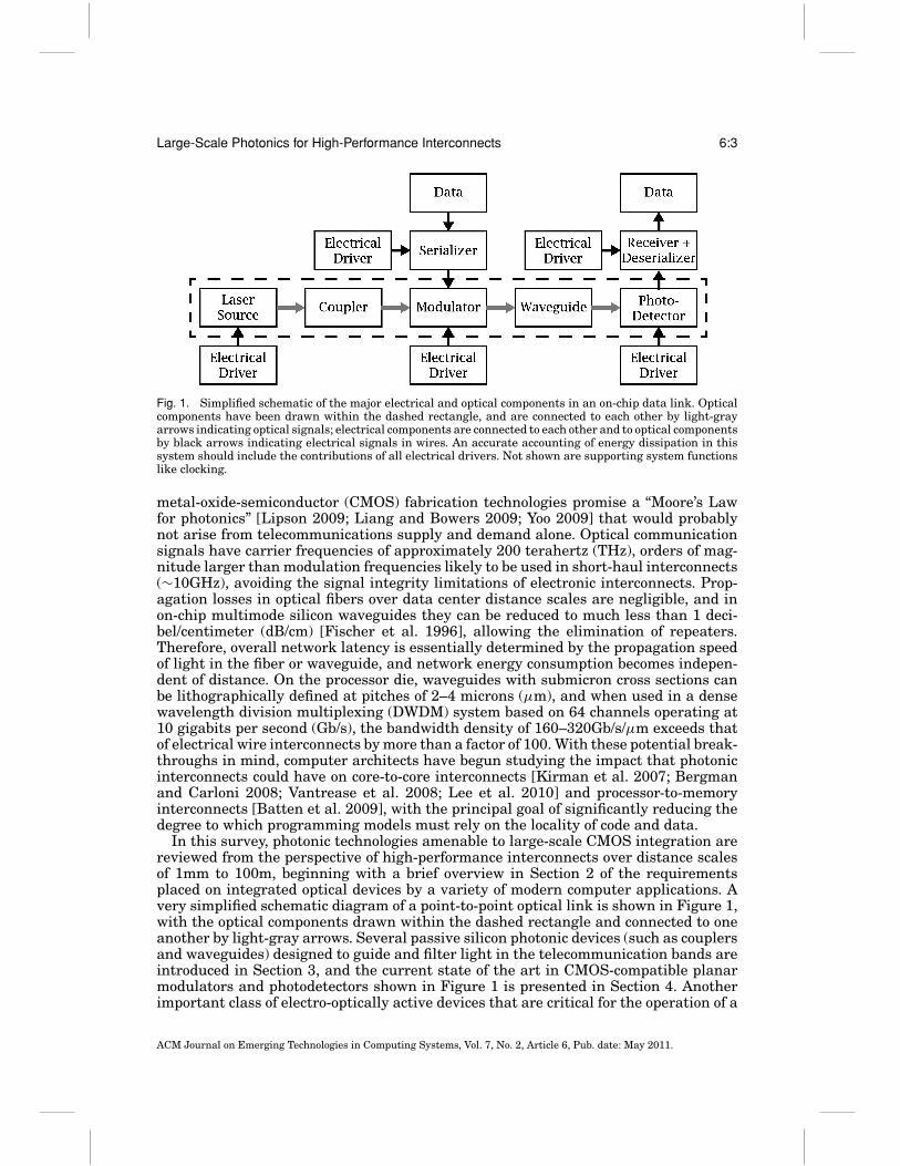
Fig. 1. Simplified schematic of the major electrical and optical components in an on-chip data link. Opticalcomponents have been drawn within the dashed rectangle, and are connected to each other by light-grayarrows indicating optical signals; electrical components are connected to each other and to optical componentsby black arrows indicating electrical signals in wires. An accurate accounting of energy dissipation in thissystem should include the contributions of all electrical drivers. Not shown are supporting system functionslike clocking.
metal-oxide-semiconductor (CMOS) fabrication technologies promise a “Moore’s Lawfor photonics” [Lipson 2009; Liang and Bowers 2009; Yoo 2009] that would probablynot arise from telecommunications supply and demand alone. Optical communicationsignals have carrier frequencies of approximately 200 terahertz (THz), orders of mag-nitude larger than modulation frequencies likely to be used in short-haul interconnects(∼10GHz), avoiding the signal integrity limitations of electronic interconnects. Prop-agation losses in optical fibers over data center distance scales are negligible, and inon-chip multimode silicon waveguides they can be reduced to much less than 1 deci-bel/centimeter (dB/cm) [Fischer et al. 1996], allowing the elimination of repeaters.Therefore, overall network latency is essentially determined by the propagation speedof light in the fiber or waveguide, and network energy consumption becomes indepen-dent of distance. On the processor die, waveguides with submicron cross sections canbe lithographically defined at pitches of 2–4 microns (μm), and when used in a densewavelength division multiplexing (DWDM) system based on 64 channels operating at10 gigabits per second (Gb/s), the bandwidth density of 160–320Gb/s/μm exceeds thatof electrical wire interconnects by more than a factor of 100. With these potential break-throughs in mind, computer architects have begun studying the impact that photonicinterconnects could have on core-to-core interconnects [Kirman et al. 2007; Bergmanand Carloni 2008; Vantrease et al. 2008; Lee et al. 2010] and processor-to-memoryinterconnects [Batten et al. 2009], with the principal goal of significantly reducing thedegree to which programming models must rely on the locality of code and data.
In this survey, photonic technologies amenable to large-scale CMOS integration arereviewed from the perspective of high-performance interconnects over distance scalesof 1mm to 100m, beginning with a brief overview in Section 2 of the requirementsplaced on integrated optical devices by a variety of modern computer applications. Avery simplified schematic diagram of a point-to-point optical link is shown in Figure 1,with the optical components drawn within the dashed rectangle and connected to oneanother by light-gray arrows. Several passive silicon photonic devices (such as couplersand waveguides) designed to guide and filter light in the telecommunication bands areintroduced in Section 3, and the current state of the art in CMOS-compatible planarmodulators and photodetectors shown in Figure 1 is presented in Section 4. Anotherimportant class of electro-optically active devices that are critical for the operation of a
ACM Journal on Emerging Technologies in Computing Systems, Vol. 7, No. 2, Article 6, Pub. date: May 2011.
6:4 R. G. Beausoleil
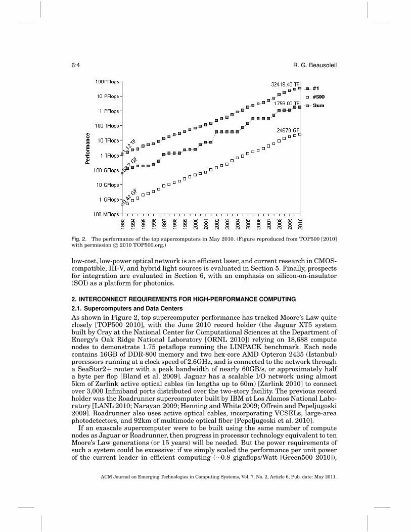
Fig. 2. The performance of the top supercomputers in May 2010. (Figure reproduced from TOP500 [2010]with permission c© 2010 TOP500.org.)
low-cost, low-power optical network is an efficient laser, and current research in CMOS-compatible, III-V, and hybrid light sources is evaluated in Section 5. Finally, prospectsfor integration are evaluated in Section 6, with an emphasis on silicon-on-insulator(SOI) as a platform for photonics.
2. INTERCONNECT REQUIREMENTS FOR HIGH-PERFORMANCE COMPUTING
2.1. Supercomputers and Data Centers
As shown in Figure 2, top supercomputer performance has tracked Moore’s Law quiteclosely [TOP500 2010], with the June 2010 record holder (the Jaguar XT5 systembuilt by Cray at the National Center for Computational Sciences at the Department ofEnergy’s Oak Ridge National Laboratory [ORNL 2010]) relying on 18,688 computenodes to demonstrate 1.75 petaflops running the LINPACK benchmark. Each nodecontains 16GB of DDR-800 memory and two hex-core AMD Opteron 2435 (Istanbul)processors running at a clock speed of 2.6GHz, and is connected to the network througha SeaStar2+ router with a peak bandwidth of nearly 60GB/s, or approximately halfa byte per flop [Bland et al. 2009]. Jaguar has a scalable I/O network using almost5km of Zarlink active optical cables (in lengths up to 60m) [Zarlink 2010] to connectover 3,000 Infiniband ports distributed over the two-story facility. The previous recordholder was the Roadrunner supercomputer built by IBM at Los Alamos National Labo-ratory [LANL 2010; Narayan 2009; Henning and White 2009; Offrein and Pepeljugoski2009]. Roadrunner also uses active optical cables, incorporating VCSELs, large-areaphotodetectors, and 92km of multimode optical fiber [Pepeljugoski et al. 2010].
If an exascale supercomputer were to be built using the same number of computenodes as Jaguar or Roadrunner, then progress in processor technology equivalent to tenMoore’s Law generations (or 15 years) will be needed. But the power requirements ofsuch a system could be excessive: if we simply scaled the performance per unit powerof the current leader in efficient computing (∼0.8 gigaflops/Watt [Green500 2010]),
ACM Journal on Emerging Technologies in Computing Systems, Vol. 7, No. 2, Article 6, Pub. date: May 2011.

Large-Scale Photonics for High-Performance Interconnects 6:5
an exaflop-class machine would require over a gigawatt of continuous power. A majorchallenge for the large-scale computer industry will be to improve this specification by afactor of 25 to approximately 20 gigaflops/Watt, enabling an exascale system to operatewith 50 megawatts of aggregate electrical power. If we assume that approximately 40%of this energy consumption is used by the transistors in the cores and main memory,and another 40–50% by the hard drives and cooling system, this leaves only 10–20% ofthe system power for the interconnect at all levels. It is clear that optics will be neededto meet this requirement [Benner 2009; Pepeljugoski et al. 2010], and it is likely thatsilicon photonics will become necessary to lower costs and enable DWDM for increasedbandwidth per connector.
While it is difficult to predict the demand for exaflop-class supercomputers in thenext decade, market trends already indicate that many data centers with exascalestorage and communication capacity will be required during the same time frame [Glick2008; Astfalk 2009; Morris 2009]. Unlike the highly parallel nature of the processingdone by Jaguar or Roadrunner, data center traffic is highly random and will requireinterconnect bandwidths at least as high as that of a supercomputing system. In 2007,data equivalent to 650,000 copies of the entire contents of the Library of Congress(nominally 1013 bytes) were transmitted over the Internet every month, and at thattime the five-year-forward compound annual growth rate in traffic was expected tobe 46% [Astfalk 2009]. HP has announced long-term plans to instrument the earthwith over one trillion sensors, each capable of generating and transmitting data at 1–1000kb/s, requiring an Internet bandwidth about 1,000 times greater than in 2007 [HP2010]. If estimates are correct that every byte transmitted over the Internet causesO(106) bytes of data communications within at least one data center, the implicationsfor data center interconnects at the end of this decade are dire [Astfalk 2009].
2.2. Computer and Network Architectures
Computer architects have long anticipated the limitations of electrical interconnects aselectronic devices shrink [Meindl et al. 2002], and a number of proposals have appearedrecently to incorporate optics at deeper levels in integrated circuits. For example, oneapproach advocated replacing the long global wires of a multicore processor with anoptical broadcast bus [Kirman et al. 2007], and another advanced a circuit-switchedphotonic network that could significantly improve the performance of GPU-like chiparchitectures [Bergman and Carloni 2008; Lee et al. 2010]. By contrast, Figure 3 showsthe physical layout of the “Corona” architecture for a processor with 256 cores dividedinto 64 groups, targeted for a 16nm process available in 2017 [Vantrease et al. 2008;Beausoleil et al. 2008; Ahn et al. 2009a]. Three of the four stacked physical layers, eachfabricated on a separate special-purpose die [Black et al. 2006], are shown: the cores(each with an integrated L1 cache), the L2 caches (shared by each group), and the globalphotonic interconnect. The silicon photonic layer is an all-to-all DWDM crossbar withfiber-optic connections to DRAM, allowing high-bandwidth and low-latency communi-cation to all memory in the system at an energy cost of approximately 290 femtojoulesper bit (fJ/b). The design is enabled by some of the active photonic devices discussedin Section 4, such as silicon microring modulators, each operating at 10Gb/s (or twicethe target clock frequency of 5GHz), and integrated silicon-germanium photodetectors.The extremely high degree of parallelism provided by this design is enabled by overpro-visioning the active photonic devices by a factor of 64 above those in use at any giventime (accounting for half of the energy consumed by the photonic layer [Ahn et al.2009a]), placing stringent requirements on the quality of the fabrication and integra-tion technologies described in Section 6. High-bandwidth arbitration is provided by anintegrated photonic system (arguably a simple, but useful, optical computer) based onthe same components used in the interconnect, with a speed that is limited only by the
ACM Journal on Emerging Technologies in Computing Systems, Vol. 7, No. 2, Article 6, Pub. date: May 2011.

6:6 R. G. Beausoleil
Fig. 3. Physical layout of the Corona architecture for a processor with 256 cores divided into 64 groups.Three of the four stacked physical layers—each integrated on a separate die—are shown: the cores (eachwith an integrated L1 cache), the L2 caches (shared by each group), and the global photonic interconnect.The L2 caches are connected via the photonics through an analog electronic driver layer (not shown). Fast,high-bandwidth arbitration is provided in the photonic layer by the same types of components used in theinterconnect. (Figure reproduced from Vantrease et al. [2008] with permission c© 2008 IEEE.)
time required for a light signal to propagate through a silicon waveguide once aroundthe chip [Vantrease et al. 2008, 2009].
An alternative architecture that also provides photonic cross-chip global interconnec-tion between groups of cores, but emphasizes processor-to-main memory communica-tion, is the “local meshes to global switches” (LMGS) topology shown in Figure 4 [Battenet al. 2009]. The optical microring filter matrix supports a processor with 256 cores (di-vided into 16 groups) and 16 DRAM modules operating at a clock speed of 2.5GHz. Thislayout is targeted toward a 400mm2 die fabricated using a 22nm technology, with apoly-crystalline silicon photonic layer implemented on the back of the silicon logic layer.The active and passive devices are under-etched using a novel approach to provide theoptical cladding discussed in Section 3; models of this technology show great promise,but as discussed in Section 4 research on the performance of polysilicon active devicesis relatively immature compared to that on pure crystalline devices. Performance sim-ulations of the LMGS interconnect architecture predict that photonics enables almostan order of magnitude improvement in bandwidth to DRAM at similar latency andpower consumption of an electrical interconnect, with an energy consumption of only250fJ/b.
Steering the computer industry toward photonic interconnects in and between pro-cessors and memory will require a nontrivial collaboration of multinational semicon-ductor and information technology companies. A nearer-term realization of a photonicapplication-specific integrated circuit (PhASIC) that could have a substantial impact
ACM Journal on Emerging Technologies in Computing Systems, Vol. 7, No. 2, Article 6, Pub. date: May 2011.

Large-Scale Photonics for High-Performance Interconnects 6:7
Fig. 4. Schematic of an optical microring filter matrix implementation of a local meshes to global switchestopology for a processor with 256 cores (divided into 16 groups indicated on each member core with a hexnumber) and 16 DRAM modules. The global interconnect channel linking core group 3 to DRAM module 0is highlighted. (Figure reproduced from Batten et al. [2009] with permission c© 2009 IEEE.)
on supercomputer and data center performance may be an optically-enabled networkswitch. “HyperX” has been proposed as a network architecture (adapted from hyper-cube and flattened butterfly topologies) that could take advantage of the high-radixswitch implementations that large-scale integrated photonics could enable [Ahn et al.2009b]. HyperX relies on a new adaptive routing algorithm that allows a favorablebalance to be found between performance, power, wiring complexity, and fault toler-ance. This approach can provide performance levels equivalent to those of a folded-Closarchitecture, with fewer switches, and uses photonic components to enable a low-costpackaging strategy for exascale data centers.
2.3. Device and Component Requirements
During the next decade, requirements for lower cost and power dissipation, reducedlatency, smaller physical size, and higher levels of integration with mainstream sili-con electronics will create inexorable pressure toward adoption of CMOS-compatiblephotonics. Although it is useful to use the ITRS roadmap [ITRS 2009] to extrapolateinterconnect performance requirements over the next ten years [Beausoleil et al. 2008;Miller 2009], the recent leveling-off of on-chip clock speeds around 3GHz [Muller 2005]makes the long-term ITRS projections of on-chip/off-chip clock rates of 14.3/67.5GHzseem highly unlikely to be realized. Furthermore, projections of processor power scaledto the 16nm technology node predict that the total processor, cache, memory controller,and intermediate electronic interconnect of a 10-teraflops multicore CPU should dissi-pate between 82 and 155 watts (W) [Vantrease et al. 2008]. If we double the half-byteper flop supercomputer bandwidth discussed above to accommodate random data cen-ter traffic, then the bidirectional on-chip and off-chip communication bandwidth shouldbe 20 terabytes/second (TB/s). Therefore, an interconnect that consumes no more than
ACM Journal on Emerging Technologies in Computing Systems, Vol. 7, No. 2, Article 6, Pub. date: May 2011.

6:8 R. G. Beausoleil
30% of the power used by the cores (consistent with ITRS interconnect projections)should operate with an energy cost of 150–300fJ/b.
This tight constraint on dissipated power discourages the use of serialization anddeserialization (SERDES), so at best a particular physical channel may operate attwice the clock frequency (i.e., read or write two bits per clock to/from digital registers),or 10Gb/s if it is assumed that on-chip and off-chip clock rates grow to 5 GHz overthe next decade. Therefore, 16,000 point-to-point physical channels will be needed toconnect cores to each other and to memory with a total bidirectional bandwidth of20TB/s, and even more would be needed for an all-to-all crossbar [Ahn et al. 2009a]. Inprinciple, a point-to-point interconnect could be implemented in a tall package usinga free-space optical interconnect built with arrays of VCSELs, photodetectors, andMEMS-actuated mirrors [Xue et al. 2008], but (assuming that the packaging issuescan be solved using the wafer-bonding techniques described in Section 5) differentinterconnect technologies would still be required for interconnects to memory andother off-chip resources. Although over the next several years integrated single-channelphotonics or multilaser coarse wavelength-division multiplexing (CWDM) could beused to communicate between packages, in the long term the use of DWDM in opticalinterconnects is inevitable, and would allow the 20 TB/s bandwidth requirement to bemet with a single photonic global interconnect layer using 64-wavelength DWDM [Xuet al. 2006; Vantrease et al. 2008; Beausoleil et al. 2008; Ahn et al. 2009a; Manipatruniet al. 2010b].
Based on these observations, in the following sections the current state of the art ofCMOS-compatible photonic devices is evaluated, and their future prospects for mono-lithic integration are assessed from the perspective of the high-bandwidth interconnectrequirements developed thus far. Key components shown in Figure 1 include:
Low-loss SOI waveguides. Waveguides fabricated on SOI using standard photolitho-graphic patterning and reactive ion etching techniques have measured losses as low as0.2dB/cm [Liu et al. 2004b], and there are indications that losses as low as 0.1 dB/cm arewithin reach [Dong et al. 2010c]. However, as discussed in Section 6, the commerciallyavailable SOI wafers used for this purpose today have top silicon layers with poorlycontrolled thicknesses, and result in fabricated devices that require “trimming” intocompliance.
Low-power germanium photodetectors. Germanium has a smaller bandgap than sili-con (0.7eV compared to 1.1eV), allowing detection of optical signals in the InternationalTelecommunication Union (ITU) wavelength bands near 1310nm (O-band) or 1550nm(C-band). As described in Section 4, monolithically integrated Ge-on-Si photodetectorsoffer the possibility of low-capacitance detectors that eliminate the need for power-hungry amplifiers and clock recovery to build a nearly “receiverless” detection scheme[Bhatnagar et al. 2004] for data rates (per channel) of 5Gb/s. At higher data rates, thegain of the transimpedance amplifier can be modest, and the clock signal can be sharedby detector arrays in a WDM system.
Resonant modulators. In DWDM systems, the ring resonators described in Section 3selectively modulate a single wavelength on a given waveguide, and can be moved toan “OFF” state where they are transparent to the data flux in the waveguide. Usingmethods outlined in Section 4, modulators work by changing the index of silicon usingcarrier injection, depletion, or accumulation. Published results indicate that the targetmodulation rate of 10Gb/s with energy consumptions as low as a few femtojoules per bitcan be achieved with CMOS technology [Xu et al. 2007; Manipatruni et al. 2007b; Wattset al. 2008a; Zortman et al. 2010a]. These devices will need to be kept resonant with thechosen wavelength by thermal and/or current tuning of their refractive indices. Sincethe incident power needed to shift the resonance of a typical compact silicon microring
ACM Journal on Emerging Technologies in Computing Systems, Vol. 7, No. 2, Article 6, Pub. date: May 2011.

Large-Scale Photonics for High-Performance Interconnects 6:9
Table I.Sellmeier coefficients for silicon in Eq. (2), valid over the ranges 20K ≤T ≤ 300K and 1.1μm ≤ λ ≤ 5.6μm. Units are K− j .
j S1 j S2 j S3 j0 1.04907E+01 −1.34661E+03 4.42827E+071 −2.08020E−04 2.91664E+01 −1.76213E+062 4.21694E−06 −2.78724E−01 −7.61575E+043 −5.82298E−09 1.05939E−03 6.78414E+024 3.44688E−12 −1.35089E−06 1.03243E+02
j �1 j �2 j �3 j0 2.99713E−01 −3.51710E+03 1.71400E+061 −1.14234E−05 4.23892E+01 −1.44984E+052 1.67134E−07 −3.57957E−01 −6.90744E+033 −2.51049E−10 1.17504E−03 −3.93699E+014 2.32484E−14 −1.13212E−06 2.35770E+01
resonator [Xu et al. 2008] by one linewidth is approximately 50mW [Soljacic et al. 2002;Leuthold et al. 2010], an aggregate optical input power of ∼3W is the upper limit fora single-waveguide 64-channel DWDM system. Careful consideration of the numberof channels that can fit within a single ring’s “free spectral range” is another criticalsystem parameter [Manipatruni et al. 2010b].
Multiwavelength lasers. Multichannel light sources for low-cost DWDM systems withprecisely controlled and locked frequency intervals are treated in Section 5. One of thepossible approaches is the Fabry-Perot comb laser based on quantum dots [Kovsh et al.2007], which has already been used to demonstrate a bit-error-rate of 10−13 at 10Gb/sover ten longitudinal modes [Gubenko et al. 2007; Innolume 2010]. Another possibleapproach is the mode-locked hybrid Si/III-V evanescent laser [Koch et al. 2007], whichuses a silicon-waveguide laser cavity wafer-bonded to a III-V gain region. The laserneed only provide 1–2W of total optical power over 64 wavelength channels to supplya 20TB/s network if the detector capacitance is low enough that only 10,000 photonsare needed to drive a 1V swing at the detector’s output terminal [Vantrease et al. 2008;Ahn et al. 2009a].
3. PASSIVE SILICON PHOTONIC DEVICES: WAVEGUIDES, FILTERS, AND COUPLERS
Silicon is transparent at wavelengths longer than 1.1μm (corresponding to energies be-low the bandgap of 1.12eV), and has a refractive index with a dependence on wavelengthand temperature that can be modeled by a Sellmeier equation as [Frey et al. 2006]
n2(λ, T ) − 1 =3∑
i=1
si(T )λ2
λ2 − λ2i
, (1)
where λ = c/ f is the vacuum wavelength in microns of an electromagnetic field withoptical frequency f , c is the speed of light, T is the temperature in degrees Kelvin,
si(T ) ≡4∑
j=0
Sij T j, and (2a)
λi(T ) ≡4∑
j=0
�i j T j . (2b)
The Sellmeier coefficients Sij and �i j for silicon are given in Table I [Frey et al.2006]. Generally, the form of Equation (1) and Equation (2) are chosen to allow
ACM Journal on Emerging Technologies in Computing Systems, Vol. 7, No. 2, Article 6, Pub. date: May 2011.

6:10 R. G. Beausoleil
Fig. 5. Plot of the phase and group refractive indices of silicon as a function of vacuum wavelength at atemperature of 300K.
Fig. 6. High-index-contrast step-index waveguides for small-footprint large-scale integration. (a) Cross-section of a step-index ridge waveguide. In SOI, the substrate is SiO2 (on silicon) and has a refractive indexof ∼1.5 in the telecom band, and the Si top layer has a material index of 3.5. The cladding layer could beair or a passivating material similar to SiO2. (b) An SEM picture of a silicon wire microring resonator with1.5μm radius adjacent to a tapered bus waveguide. The field circulating in the ring is coupled to the buswaveguide through evanescent field leakage from the outer surface of the ring. (Figure 6(b) reproduced fromXu et al. [2008] with permission c© 2008 OSA.)
an accurate fit to available optical data, and allow computation of the dispersion(dn(λ, T )/dλ), the group refractive index (ng(λ, T ) = n(λ, T ) − λ∂n(λ, T )/∂λ), and thethermooptic coefficient (dn(λ, T )/dT ) at wavelengths and temperatures where directmeasurements are not available. A plot of the refractive index (also as known as thephase index) and the group refractive index of silicon as a function of wavelength andtemperature is shown in Figure 5.
3.1. Waveguides
The waveguides most commonly used in large-scale silicon integrated photonics arevariations of the dielectric slab waveguide [Hu and Menyuk 2009] that is now com-monly treated in textbooks [Okamoto 2006]. As shown in Figure 6(a), the dielectricridge waveguide has a light-guiding layer with a high-index core that is defined bya ridge atop a pedestal, situated between lower-index substrate and cladding layers
ACM Journal on Emerging Technologies in Computing Systems, Vol. 7, No. 2, Article 6, Pub. date: May 2011.
Large-Scale Photonics for High-Performance Interconnects 6:11
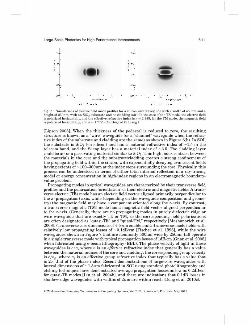
Fig. 7. Simulations of electric field mode profiles for a silicon wire waveguide with a width of 450nm and aheight of 250nm, with an SiO2 substrate and no cladding (air). In the case of the TE mode, the electric fieldis polarized horizontally, and the effective refractive index is n = 2.385, for the TM mode, the magnetic fieldis polarized horizontally, and n = 1.772. (Courtesy of Di Liang.)
[Lipson 2005]. When the thickness of the pedestal is reduced to zero, the resultingstructure is known as a “wire” waveguide (or a “channel” waveguide when the refrac-tive index of the substrate and cladding are the same) as shown in Figure 6(b). In SOI,the substrate is SiO2 (on silicon) and has a material refractive index of ∼1.5 in thetelecom band, and the Si top layer has a material index of ∼3.5. The cladding layercould be air or a passivating material similar to SiO2. This high index contrast betweenthe materials in the core and the substrate/cladding creates a strong confinement ofthe propagating field within the silicon, with exponentially decaying evanescent fieldshaving extents of ∼100–300nm at the index steps surrounding the core. Physically, thisprocess can be understood in terms of either total internal reflection in a ray-tracingmodel or energy concentration in high-index regions in an electromagnetic boundary-value problem.
Propagating modes in optical waveguides are characterized by their transverse fieldprofiles and the polarization (orientation) of their electric and magnetic fields. A trans-verse electric (TE) mode has an electric field vector aligned primarily perpendicular tothe z (propagation) axis, while (depending on the waveguide composition and geome-try) the magnetic field may have a component oriented along the z-axis. By contrast,a transverse magnetic (TM) mode has a magnetic field vector aligned perpendicularto the z-axis. (Generally, there are no propagating modes in purely dielectric ridge orwire waveguide that are exactly TE or TM, so the corresponding field polarizationsare often designated as “quasi-TE” and “quasi-TM,” respectively [Mashanovich et al.2008].) Transverse core dimensions of 4–8μm enable multi-transverse-mode fields withrelatively low propagating losses of ∼0.1dB/cm [Fischer et al. 1996], while the wirewaveguides shown in Figure 7 that are nominally 500nm wide by 250nm tall operatein a single transverse mode with typical propagation losses of 1dB/cm [Gnan et al. 2008]when fabricated using e-beam lithography (EBL). The phase velocity of light in thesewaveguides is c/n, where n is an effective refractive index that generally has a valuebetween the material indices of the core and cladding; the corresponding group velocityis c/ng, where ng is an effective group refractive index that typically has a value thatis 2× that of the phase index. Recent demonstrations of large-core waveguides withlateral dimensions of ∼1.5μm fabricated in SOI using standard photolithography andetching techniques have demonstrated average propagation losses as low as 0.2dB/cmfor quasi-TE modes [Liu et al. 2004b], and there are indications that 0.1dB losses inshallow-ridge waveguides with widths of 2μm are within reach [Dong et al. 2010c].
ACM Journal on Emerging Technologies in Computing Systems, Vol. 7, No. 2, Article 6, Pub. date: May 2011.
6:12 R. G. Beausoleil
A number of technologies have been proposed and demonstrated to complete the setof optical components amenable to large-scale integration on-chip with CMOS compat-ible processes. Polarization rotators are commonly used in fiber-optic networks, andan offset dual-core silicon channel waveguide structure with a rotation element with awidth of ∼2μm and a length of 35μm has been demonstrated with a rotation angle of72◦ and a polarization extinction ratio of 11dB [Fukuda et al. 2008], and a design basedon coupling through an intermediate multimode waveguide with similar dimensionshas been proposed that promises 90◦ rotation with an extinction ratio as high as 17dB[Yue et al. 2009]. Although none of the architectures described in Section 2 requirepurely passive crossed waveguides, as optical circuit element density grows, waveg-uide intersections in the silicon plane may become necessary. SOI waveguides withcrossings showing losses of −0.16dB and cross-talk of −40dB have been demonstrated,based on a design incorporating parabolically broadened waveguides to reduce lateralrefractive index contrast while maintaining high lateral mode confinement [Bogaertset al. 2007]. Models show that similar results could be obtained with more conventionalplanar patterning and etching [Li et al. 2009]. However, an intriguing new approach toCMOS-compatible waveguides relies on refractive index engineering using subwave-length gratings rather than ridge or wire waveguides. This approach has been used todemonstrate index-guided waveguides fabricated in a single etch step with propagationlosses as low as 2.1dB/cm with a low group index of ng ≈ 1.5 over the entire telecomC-band [Bock et al. 2010a]. When crossed waveguides are fabricated using the sameapproach, the loss per crossing was measured to be as low as −0.02dB with crosstalkless than −40dB [Bock et al. 2010b]. Other compact planar photonic devices such asinput couplers and multiplexor circuits have also been implemented with performancecharacteristics comparable to those of ridge and wire waveguides [Cheben et al. 2010].
One of the principal contributions to the propagation and scattering losses of single-mode high-index-contrast (HIC) channel and ridge waveguides is the roughness of thesidewalls induced by patterning and etching processes, causing the observed loss ratesof ∼1dB/cm that are two orders of magnitude higher than those of low-index-contrastwaveguides such as optical fiber. This optical loss is not simply incoherent scatteringfrom random surface perturbations into the substrate or cladding; rather, a nontrivialfraction of the scattered power has been found to couple to backward-propagating modesin HIC waveguides [Morichetti et al. 2010a, Morichetti et al. 2010b]. This backscatter-ing can be extensive even in single-mode waveguides only a few hundred micrometersin length, creating a possible barrier to some applications of high-density photonicintegrated circuits. A model of the scattering process is shown in Figure 8(a) for awaveguide of length Lw and nominal width w with rough sidewall surfaces. The com-plex backscattering amplitude hR(z) for a waveguide segment of length dz depends onthe average loss coefficient α ∼= (π/λB)(∂n/∂w)δw, where λB is the Bragg wavelengthcorresponding to a simple sinusoidal corrugation in the waveguide sidewalls havingamplitude δw, and n is the effective index of the waveguide. In the small perturbationregime, the backscattered power is proportional to |α|2, and as shown in Figure 8(b) canreach nontrivial values for TE polarizations over relatively short distances. These mea-surements were performed on waveguides fabricated using EBL [Gnan et al. 2008], andshould be repeated for guides fabricated using high-resolution CMOS photolithographyand etching technologies.
3.2. Filters
A complete toolbox of silicon-based optical components that enable low-cost, compact,and/or WDM interconnect applications should include passive multiplexors and demul-tiplexors, splitters/couplers, and filters. These generally fall into two classes: nonreso-nant devices, which are well studied and understood and tend to have comparatively
ACM Journal on Emerging Technologies in Computing Systems, Vol. 7, No. 2, Article 6, Pub. date: May 2011.

Large-Scale Photonics for High-Performance Interconnects 6:13
Fig. 8. Backscattering induced by sidewall roughness in high-index-contrast SOI channel waveguides.(a) Model of a waveguide of length Lw and nominal width w with rough sidewall surfaces. The complexbackscattering amplitude hR(z) for a waveguide segment of length d z depends on the average loss coefficientα. (b) Measurements of the backscattered power spectral density for an SOI waveguide with Lw = 1mmand w = 490nm for TE (solid curve) and TM (dotted curve) input polarization. (Figure reproduced fromMorichetti et al. [2010b] with permission c© 2010 OSA.)
large footprints in silicon photonic integrated circuits; and resonant devices (such asmicroring cavities) which can be quite compact, but with sensitivities to environmentalperturbations that present particular challenges for integration.
3.2.1. Nonresonant Couplers and Filters. The simplest nonresonant coupler, the 1 × 2Y -junction beamsplitter, can be cascaded to distribute optical power over many waveg-uides with low loss, minimal sensitivity to wavelength, and even power distributionover the output ports [Tao et al. 2008]. SOI-based multimode interference couplers alsodivide power from a single input port to multiple output ports by relying on spatialinterference in an intermediary slab region [Lipson 2005; Jiao et al. 2010]. Wavelength-division multiplexing applications may require that different wavelength channels bedistributed into different waveguides, requiring spectral filters such as an arrayedwaveguide or echelle grating [Bogaerts et al. 2010].
Perhaps the most commonly used spectral filter in CMOS-compatible WDM photonicsis the silicon-wire Mach-Zehnder interferometer shown schematically in Figure 9. Thenarrowband input field Ein enters the device through a single-mode wire waveguide, issplit into two equal parts by a Y -junction or multimode interference coupler, and thenis recombined using the same structure to produce the output field Eout. The field in theupper waveguide propagates through a section of length L containing an integratedresistive heater [Liu et al. 2010a] which changes the local temperature by �T , causinga change in the effective refractive index �n = (dn/dT )�T , where the thermooptic
ACM Journal on Emerging Technologies in Computing Systems, Vol. 7, No. 2, Article 6, Pub. date: May 2011.

6:14 R. G. Beausoleil
Fig. 9. Schematic of a silicon Mach-Zehnder interferometer used as a spectral filter. An input field is splitby a 3-dB Y -junction or multimode interference coupler, and the mode in the upper arm is phase-shifted byan integrated resistive heater. When the beams are recombined in another 3-dB coupler, the magnitude andphase of the output field depends on the applied phase shift.
coefficient dn/dT ≈ 2×10⁻⁴ K−1 for highly-confined modes in silicon [Frey et al. 2006].In this case, the output field is given by
Eout(φ) = 12
(1 + eiφ)Ein, (3)
where φ = 2π�nf L/c and f is the optical (carrier) frequency of both fields. The outputpower of the interferometer is proportional to
|Eout(φ)|2 = cos2(
φ
2
)|Ein|2 . (4)
Therefore, if �T is chosen so that φ = 2mπ for some integer m (equivalent to thecondition �nL = mλ) the fields in both arms constructively interfere at the outputcoupler, and Eout = Ein. However, if φ = (2m+ 1)π , the fields destructively interfere,and Eout = 0. There are a number of variations on this simple design; for example,the waveguides in the arms can be fabricated with different lengths to optimize filterperformance at a particular wavelength for �T = 0, but special care is then requiredto reduce the sensitivity of the entire device to ambient temperature [Uenuma andMoooka 2009].
3.2.2. Resonant Couplers and Filters. A particularly relevant example of a resonant filteris the two-port microring resonator shown in Figure 10(a) consisting of two bus waveg-uides and a ring waveguide with an effective refractive index n and power absorbtioncoefficient α. The mean radius of the ring, measured at the center of the circularwaveguide, is a, and the perimeter is p = 2πa. Light is weakly coupled between thecurved waveguides and the nearby straight bus waveguides through the short-rangeevanescent fields leaking from both structures. The magnitude and phase of thesecouplings are determined by the dimensions of the waveguides and the separation be-tween them, and are represented by the (ideally) broadband power reflectance R1,2 andtransmittance T1,2 at ports 1 and 2. (For the time being, we neglect backscattering inall waveguides, but we include the effects of dissipative optical loss in the couplers byallowing R1,2 + T1,2 ≤ 1.) The microring resonator shown in Figure 6(b) [Xu et al. 2008]is a single-port device with R2 = 1 and T2 = 0. A narrowband input field Ein producesan output field Eout at port 1 and a cross-coupled field Exc at port 2, given by
Eout(φ) = 1√R1
R1 − (R1 + T1)eiφ
1 − eiφEin, (5a)
Exc(φ) =√
T1T2e−αp/2 eiφ/2
1 − eiφEin, (5b)
ACM Journal on Emerging Technologies in Computing Systems, Vol. 7, No. 2, Article 6, Pub. date: May 2011.
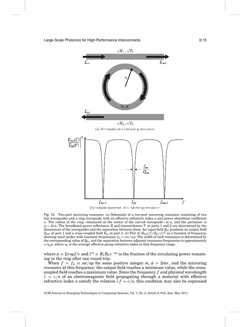
Large-Scale Photonics for High-Performance Interconnects 6:15
Fig. 10. Two-port microring resonator. (a) Schematic of a two-port microring resonator consisting of twobus waveguides and a ring waveguide with an effective refractive index n and power absorbtion coefficientα. The radius of the ring—measured at the center of the curved waveguide—is a, and the perimeter isp = 2πa. The broadband power reflectance R and transmittance T at ports 1 and 2 are determined by thedimensions of the waveguides and the separation between them. An input field Ein produces an output fieldEout at port 1 and a cross-coupled field Exc at port 2. (b) Plot of |Eout( f )/Ein( f )|2 as a function of frequency,showing axial modes with resonant frequencies fm = mc/np. The width of each resonance is determined bythe corresponding value of Qm, and the separation between adjacent resonance frequencies is approximatelyc/ng p, where ng is the average effective group refractive index in that frequency range.
where φ ≡ 2πnpf/c and 2 ≡ R1 R2 e−αp is the fraction of the circulating power remain-ing in the ring after one round trip.
When f = fm ≡ mc/np for some positive integer m, φ = 2mπ , and the microringresonates at this frequency: the output field reaches a minimum value, while the cross-coupled field reaches a maximum value. Since the frequency f and physical wavelengthλ = λ/n of an electromagnetic field propagating through a material with effectiverefractive index n satisfy the relation λ f = c/n, this condition may also be expressed
ACM Journal on Emerging Technologies in Computing Systems, Vol. 7, No. 2, Article 6, Pub. date: May 2011.

6:16 R. G. Beausoleil
in terms of wavelength as mλm = p; in other words, a resonance is obtained wheneveran integer number of physical wavelengths fits exactly around the ring perimeter.The value of the frequency fm will shift when the mode index m, perimeter p, or therefractive index n change. If these variations are small enough that we can ignoresecond-order terms in the Taylor expansion, then
δ fm
fm= δm
m− δp
p− δn
n. (6)
Now the effective refractive index n ≡ n( f, T , q) may vary due to changes in the fre-quency itself, the temperature T , and (as discussed in Section 4.1.1) the local carrierdensity q, according to
δn = ∂n∂ f
δ f + ∂n∂T
δT + ∂n∂q
δq, (7)
so that the fractional shift in the resonance frequency of longitudinal mode m becomes
δ fm
fm= n
ng
[δmm
− δpp
]− 1
ng
[∂n∂T
δT + ∂n∂q
δq]
, (8)
where ng = n + f ∂n/∂ f is the effective group refractive index introduced earlier as afunction of the vacuum wavelength. Similar considerations show that the correspond-ing fractional change in the physical wavelength is δλ/λ = −(ng/n) δ f/ f . As an exampleof the utility of Equation (8), in the case where δm = ±1, δp = 0, δT = 0, and δq = 0, thecorresponding frequency separation between adjacent minima in |Eout|2 is known asthe free spectral range and is given by � fFSR = c/ng p. In general, careful simulationsof the transverse and longitudinal eigenmodes of microring resonators will also dependon the waveguide width and height, and on the refractive indices of the substrate andcladding.
Given values of α, R2, and any dissipative losses in port 1, if we choose the dimensionsof the waveguides in port 1 so that R1 = (R1 + T1), then the ring is critically coupled,with
Eout(φ) =√
R11 − eiφ
1 − eiφEin. (9)
In this ideal case, whenever the frequency f = fm, the output power vanishes, and asshown in Figure 10(b), at frequencies midway between fm and fm+1 the output powerachieves a maximum value proportional to |Eout|2 = |Ein|24R1/(1 + )2. At a frequencyf = fm + � f , where � f � � fFSR, Equation (9) may be approximated by
Eout(� f ) =√
R1
−i� f � fm/2 + [2√
/(1 + )]� f 2
� f 2 + (� fm/2)2Ein( f ), (10)
where � fm ≡ fm/Qm, and
Qm ≡ mπ
√
1 − . (11)
As shown in Figure 10(b), the denominator in Eq. (10) characterizes a Lorentzianresonance with a full-width at half-maximum of � fm.
Both the precise values of the resonance frequencies fm and the quality factors Qmof the ring are determined by the details of the ring geometry, the core material, andthe sidewall roughness of the ring waveguide [Lipson 2005; Xu et al. 2008]. Althoughit is clear that both intrinsic absorption by the core material (generally negligiblein silicon at telecommunication wavelengths) and the scattering by the core sidewall
ACM Journal on Emerging Technologies in Computing Systems, Vol. 7, No. 2, Article 6, Pub. date: May 2011.

Large-Scale Photonics for High-Performance Interconnects 6:17
Fig. 11. Model of the intrinsic optical quality factor Q and waveguide bending loss versus the ra-dius for a quasi-TE mode of an uncoupled microring resonator at 1.55μm computed using a 3D finite-difference time-domain simulation. Here the SOI waveguide has a rectangular cross-section with dimensions450nm × 250nm. (Figure reproduced from Xu et al. [2008] with permission c© 2008 OSA.)
roughness described above causes loss that depends on the ring circumference, there isa fundamental upper limit placed on Q by the curvature of the ring itself. As shown inFigure 7, because the boundaries of a straight channel or ridge waveguide are dielectricrather then metal in nature, the corresponding transverse mode profile has evanescentwings that extend beyond the high index core into the lower index cladding. In the caseof the straight waveguide, these evanescent fields have phase profiles linked to thepropagating modes within the guide, traveling at a speed c/n. In a curved waveguide,the evanescent fields on the outside of the core must travel faster than the propagatingfield in the core, and beyond a critical distance the required propagation speed for thephase front exceeds c/ncladding, coupling the evanescent fields to modes propagatingaway from the ring [Lipson 2005]. As shown in Figure 11, this bending loss creates afundamental upper limit to the intrinsic (uncoupled) Q of a microring resonator [Xuet al. 2008]. A completely uncoupled ring (i.e., with R1 = R2 = 1 and αp � 1) has anintrinsic Qm ≈ 2mπ/αp, and the same ring when critically coupled through a singleport as in Figure 6(b) with R1 = e−αp has a loaded quality factor that is smaller by afactor of 2.
Microring resonators can function as photonic integrated circuit elements in a varietyof configurations, particularly in the case where WDM is used to encode data on a combof multiple independent regularly-spaced frequency channels [Lipson 2005; Dong et al.2010b; Manipatruni et al. 2010b]. In Figure 12(a), a ring tuned off-resonance allowsall data channels to propagate through the bus waveguide, while in (b) a ring witha resonance frequency aligned with that of a particular data channel diverts lightfrom that channel into the ring, where it is scattered by the rough, curved surfaceof the ring. As described in Section 4.1.3, electrically activating this tuning at highspeed allows the microring to be used as an electro optic modulator [Xu et al. 2005;Chen et al. 2009; Lee et al. 2010]. In Figure 12(c), a ring (which need not be criticallycoupled) with two bus waveguides can be used to divert one (resonant) channel fromone waveguide to the other, and Figure 12(d) shows that incorporating a photodetectionelement (such as germanium) in a ring allows it to absorb diverted light and act as
ACM Journal on Emerging Technologies in Computing Systems, Vol. 7, No. 2, Article 6, Pub. date: May 2011.

6:18 R. G. Beausoleil
Fig. 12. Microring resonators as photonic integrated circuit elements. (a) A ring tuned off-resonance allowsall data channels to propagate through the bus waveguide. (b) A ring with a resonance frequency alignedwith that of a particular data channel diverts light from that channel into the ring, where it is scattered.(c) A ring coupled to two bus waveguides can be used to divert one (resonant) channel from one waveguideto the other. (d) Incorporating a photodetection element (such as germanium) in a ring allows it to absorbdiverted light and act as part of a receiver. (Figure reproduced from Vantrease et al. [2008] with permissionc© 2008 IEEE.)
part of a receiver. Recent research has proposed that microrings can be used to providethe optical isolation that is critical to minimize the effects of coherent backscatteringdiscussed below [Yu and Fan 2009]. Resonant structures similar to microrings, such asmicrodisks [Watts et al. 2008a; Zortman et al. 2010a; DeRose et al. 2010], offer similaropportunities for integrated photonics, but many of these devices have resonant higher-order transverse modes that are problematic for WDM architectures.
As bidirectional bandwidth across a single CMOS die scales to 10 TB/s and beyond[Vantrease et al. 2008], the increased circuit density enabled by compact resonant fil-ters, modulators, and switches will become a significant driver for large-scale integratedphotonics. A microring filter with a smaller circumference has a larger free spectralrange, allowing a larger number of microrings resonant with different, equally-spaceddata channels to be attached in a small area to a common bus waveguide carrying ahigher aggregate data bandwidth [Manipatruni et al. 2010]. In the particular case ofthe microring modulator discussed in Section 4.1.3, the power consumed by the deviceis proportional to the capacitance (and therefore the circumference) and inversely pro-portional to the Q of the ring. The electrical capacitance of devices demonstrated inthe laboratory has been reduced to a few femtofarads [Chen and Lipson 2009], lower-ing their energy consumption to ∼10fJ/b [Watts et al. 2008a; Zortman et al. 2010a].After an SOI microring resonator with a diameter of only 4 μm was incorporated into anadd/drop filter and demonstrated a Q = 6730 [Nawrocka et al. 2006], further reductionsin device footprint required careful attention to spatial and spectral mode-matching tominimize the coupling between the fundamental transverse mode of the ring’s curvedwaveguide and higher-order propagating modes in the straight bus waveguide [Xuet al. 2008]. By tapering the bus waveguide to a width of ∼290nm and increasing thegap between the the straight waveguide and the ∼440nm ring waveguide to ∼340nm,a microring resonator fabricated using EBL with a diameter of 3μm was demonstratedwith a coupled Q ≈ 9000.
In the ITU wavelength O-band and C-band, the thermooptic effect in silicon causesthe refractive index of tightly confined modes to shift with temperature by approxi-mately dn/dT ≈ 2 × 10⁻⁴ K−1. Using Equation 9, this corresponds to a temperature-dependent wavelength shift (TDWS) of a microring resonator operating near 1310nmof δλm ≈ 75pm/K—or δ fm ≈ 13GHz/K—independent of the radius of the ring. Therefore,a local temperature change of only 1K is sufficient to switch a microring coupled to abus waveguide with a Q chosen to provide a FWHM � fm = 20GHz from an “off” state
ACM Journal on Emerging Technologies in Computing Systems, Vol. 7, No. 2, Article 6, Pub. date: May 2011.

Large-Scale Photonics for High-Performance Interconnects 6:19
Fig. 13. Models of athermal coupled microring resonators based on slot waveguides incorporating polymers.(a) Schematic of a slotted-waveguide microring resonator with an inset showing a cross-section of the waveg-uide. (b) Simulated electric field profiles for TE modes in waveguides with w = 200nm and h = 250nm andvarying slot width s, showing that a substantial fraction of the mode energy is carried by the slot. (Figurereproduced from Zhou et al. [2009a] with permission c© 2009 by the authors.)
with |Eout( fm)/Eout( fm)|2 → 0 to a state where the output power is 60% of the input.Since temperature fluctuations within single-die CPU packages can exceed 40K, it isclear that the use of resonant devices in information technology applications requirestechniques that mitigate thermooptic effects. One way to reduce the impact of temper-ature shifts on a microring resonator is to couple it to another optical system (such asa Mach-Zehnder interferometer [Guha et al. 2010]) that has an effective optical pathlength nL designed to cancel changes in that of the ring, at the expense of an increasein the aggregate size of the device. Alternatively, the device footprint can be retained bychanging the structure of the ring and bus waveguides to include a high-confinementlow-index slot waveguide [Lipson 2005] that can be filled with a material (such as apolymer) that has a value of dn/dT < 0 [Lee et al. 2008; Zhou et al. 2009a]. Figure 13(a)presents a schematic of a slotted-waveguide microring resonator with an inset showinga cross-section of the waveguide, while Figure 13(b) illustrates simulated electric fieldprofiles for TE modes in waveguides with w = 200nm and h = 250nm and varying slotwidth s, showing that a substantial fraction of the mode energy is carried by the slot.Careful choice of the polymer and design of the slots and the coupling junction betweenthe ring and bus waveguides results in a cancelation of the TDWS [Lee et al. 2008],but the high field intensity at the slot sidewalls shown in Figure 13(b) causes higherlevels of surface scattering and therefore lower cavity Q [Zhou et al. 2009a]. Recently,an intermediate approach that reduces both the level of confinement and the effectiveindex of polymer-cladded silicon wire waveguides has shown a reduction of the TDWSto 0.5pm/K for TM modes [Raghunathan et al. 2010]. The reduced confinement allows agreater fraction of the transverse mode profile to extend into the polymer, but increasesthe footprint of the waveguides and resonators. One design constraint common to all of
ACM Journal on Emerging Technologies in Computing Systems, Vol. 7, No. 2, Article 6, Pub. date: May 2011.

6:20 R. G. Beausoleil
these approaches is the need to tailor the waveguide dimensions to provide the sameconfinement factor for each wavelength, complicating the design of DWDM systems.
In an integrated photonic DWDM system, the frequency channels propagate along acommon bus waveguide, interacting with devices such as modulators, filters, and de-tectors resonant with particular channels. For example, as described in Section 4.1.3,a microring resonator designed to act as a modulator for frequency channel m will cre-ate a resonant loss at frequency fm according to Equation (5a) with a magnitude thatdepends on the values of R1, T1, , and on the value of the refractive index of the ring.(However, recent measurements of coherent backscattering by microrings resonantwith an incident field show that a significant fraction of the measured round-trip lossin cavities fabricated using EBL can be caused by counterpropagating fields caused bysidewall roughness of the ring waveguide [Morichetti et al. 2010]. This effect will needto be studied for the case of critically coupled compact rings built using photolithogra-phy and CMOS materials processing.) In addition, there will be a quasi-resonant lossinduced by microrings designed to operate at channels m − 1 and m + 1. Consider acritically-coupled high-Q ring with R1 ≈ → 1 and � fm = 20GHz. If the channel spac-ing is 80GHz, then by Equation (10) the total power loss in channel m due to the tworings resonant with the adjacent channels is 2 × 10 log10 |Eout( f )/Ein( f )|2 ≈ −0.13dB.Rings more than a few channels away from m cause nonresonant losses that are notpredicted very accurately by Equation (10), because they arise from interactions of theevanescent fields of the bus waveguide and curved waveguides comprising the rings.If surface roughness is neglected, finite-difference time-domain models of the compactmicroring cavity shown in Figure 6(b) estimate that the nonresonant scattering lossalong the bus waveguide due to the presence of a nearby curved waveguide is less than−0.001dB per ring for both TE and TM modes.
As both physical component and channel densities increase to accommodate thebandwidths demanded by Moore’s Law, the Lorentzian lineshape shown in Figure 10(b)may not provide the out-of-band rejection ratios needed for adequate bit-error rates.Instead, resonant filters incorporating multiple coupled microrings can provide higher-order filter lineshapes without the complexity typical of thin-film filters [Little et al.2004; Xiao et al. 2007]. Purely passive, low-loss thermally tuned filters incorporating upto 11 microrings have been fabricated using chemical vapor deposition in Hydex withan index contrast of 17% (corresponding to a core index of 1.70 and a cladding index of1.45) [Little et al. 2004], and a third-order silicon microring add-drop filter fabricatedin SOI has been demonstrated with low loss, a passband of 125GHz, and out-of-bandsignal rejection of 40dB [Xiao et al. 2007]. More complex resonator configurations,such as microrings embedded within compact racetracks [Zhang et al. 2008a], allowfrequency responses tailored to particular applications.
4. ACTIVE SILICON PHOTONIC DEVICES: MODULATORS AND PHOTODETECTORS
4.1. Integrated CMOS-Compatible Modulators
The promise of large-scale integrated photonic interconnect links based on CMOS-compatible devices has inspired an explosion of research and development on silicon-based electro-optic modulators. A recent review of this progress by Reed et al. [2010] isquite complete and includes a table of device performance results.
4.1.1. The Physics of Silicon-Based Switches and Modulators. Optoelectronic modulatorsgenerally encode data on propagating light channels by changing the amplitude, phase,or polarization of a continuous optical field through variations in the complex propaga-tion vector of that field. In telecommunications systems, most modulators are based onsemiconductor linear and nonlinear optical mechanisms such as the Franz-Keldysh,Pockels, and Kerr effects. However, in single-crystal silicon, the magnitude of these
ACM Journal on Emerging Technologies in Computing Systems, Vol. 7, No. 2, Article 6, Pub. date: May 2011.

Large-Scale Photonics for High-Performance Interconnects 6:21
effects at the telecommunication wavelengths near 1310nm and 1550nm are too smallto allow energy-efficient operation of high-performance modulators [Soref and Ben-nett 1987]. The most promising candidates for silicon optical modulators rely on thefree-carrier plasma-dispersion effect to change the silicon refractive index by vary-ing electron and hole densities within the optical waveguide, or the quantum-confinedStark effect to vary the refractive index [Reed et al. 2010]. The thermo-optic effectin silicon is appreciable, but it is too slow to be used effectively for high-bandwidthmodulation [Lipson 2005].
Soref and Bennett used a numerical Kramers-Kronig approach to analyze absorp-tion data in pure crystalline silicon over widely varying electron and hole densities andcomputed the corresponding perturbations in the refractive index and absorption coef-ficients at telecommunications wavelengths [Soref and Bennett 1987]. For example, atan optical wavelength λ ∼= 1310nm, their results can be summarized by the formulas[Gardes et al. 2008; Reed et al. 2010]
�nSi(1310nm) = −6.2 × 10⁻²²cm3 Ne − 6.0 × 10⁻¹⁸cm2.4 N 0.8h , (12a)
�αSi(1310nm) = 6.0 × 10⁻¹⁸cm2 Ne + 4.0 × 10⁻¹⁸cm2 Nh, (12b)
and near λ = 1550nm,
�nSi(1550nm) = −8.8 × 10⁻²² cm3 Ne − 8.5 × 10⁻¹⁸ cm2.4 N 0.8h , (13a)
�αSi(1550nm) = 8.5 × 10⁻¹⁸ cm2 Ne + 6.0 × 10⁻¹⁸ cm2 Nh. (13b)
Here �nSi is the change in the (dimensionless) refractive index, �αSi is the absorptioncoefficient in cm−1, Ne is the electron density in cm−3, and Nh is the density of holes incm−3. (Note that Soref and Bennett found that the dependence of the refractive indexon the hole density is not linear, in contrast to predictions of simple free carrier orDrude theory, but instead is characterized by the exponent 0.8.) In principle, moderatechanges in carrier density should provide significant refractive index modulation, butin practice the absorption becomes a significant limit through device insertion loss. Forexample, at a carrier density of 1017cm3, we find that �n(1310nm) ≈ −3.0 × 10⁻⁴ and�α(1310nm) ≈ 1.0cm−1, and �n(1550nm) ≈ −4.3×10⁻⁴ and �α(1550nm) ≈ 1.45cm−1.
Modulators based on refractive index perturbation through the free-carrier plasma-dispersion effect generally operate in one of three modes:
Carrier injection. [Xu et al. 2005; Reed et al. 2010] As shown in Figure 14(a), thewaveguide region defining the optical mode is confined within the intrinsic region ofa p-i-n diode to avoid optical absorption losses in the heavily doped p-type and n-typeregions. When the junction is forward-biased, carriers can be injected into the waveg-uide through the doped regions in contact with metal wires, where they modify therefractive index of the intrinsic silicon. Modulators based on injection mode operationgenerally require low bias voltages (< 1 V) and allow large extinction ratios—the ra-tio of light intensities representing bit values 1 and 0 in an on-off keying modulationscheme—but are generally limited in speed by the long minority carrier lifetime ofsilicon (∼ 1ns for devices with few-micron-scale lateral dimensions). This limitationcan be partially mitigated either by using drive signal pre-emphasis [Xu et al. 2007]or through the significantly smaller device volumes available from compact microringresonators [Manipatruni et al. 2010].
Carrier depletion. If the waveguide in the carrier injection device is lightly dopedas shown in Figure 14(b), the resulting p-n diode can be operated in reverse bias todeplete carriers from a central region that has a width that depends on the appliedvoltage [Reed et al. 2010]. If the intrinsic capacitance and resistance of the deviceis low enough, then the minority carrier lifetime is no longer a significant limitation
ACM Journal on Emerging Technologies in Computing Systems, Vol. 7, No. 2, Article 6, Pub. date: May 2011.

6:22 R. G. Beausoleil
Fig. 14. Three commonly used carrier modes in silicon modulators. (a) In carrier injection, the heavily p-doped and n-doped regions are separated by the intrinsic region containing the optical waveguide to forma p-i-n junction. (b) In carrier depletion, lightly doped p-type and n-type regions contact in the waveguideregion to form a p-n junction. (c) In carrier accumulation (the MOS effect), a capacitative structure is formedby placing a thin oxide barrier in the center of the intrinsic region. (After Reed et al. [2001].)
[Liu et al. 2007; Liao et al. 2007]. The dopant concentration in the waveguide mustbe low enough to avoid significant absorption of the optical mode, thereby limitingthe maximum change in refractive index to the value obtained when the availablecarriers are fully depleted. Although forward-bias operation [Spector et al. 2010] andmore complicated diode structures are available [Rasigade et al. 2010] in depletionmode, p-n structures are commonly used to obtain low-power operation at moderatemodulation depths [Zheng et al. 2010; Watts et al. 2010; Zortman et al. 2010a].
Carrier accumulation. If the device structure of the injection-mode device is modifiedto include a thin oxide barrier at the center of the waveguide, then the metal-oxide-semiconductor (MOS) configuration shown in Figure 14(c) can be used to accumulatecarriers within the optical mode and thereby modify the local refractive index [Liu et al.
ACM Journal on Emerging Technologies in Computing Systems, Vol. 7, No. 2, Article 6, Pub. date: May 2011.

Large-Scale Photonics for High-Performance Interconnects 6:23
2004a; Barrios and Lipson 2004]. The capacitative structure enforced by the barrierallows the device to operate at speeds that depend primarily on its resistance andcapacitance rather than the minority carrier lifetime [Passaro and Dell’Olio 2008], anda device with a length less than 0.5mm recently demonstrated by Lightwire delivers a9dB extinction ratio at a data rate of 10Gb/s [D’Andrea 2009].
A promising alternative to refractive index modulation in pure silicon based onthe free-carrier plasma-dispersion effect is the electric-field-induced change in absorp-tion observed in waveguide-integrated silicon-germanium devices. For example, anelectro-absorption (EA) modulator based on the Franz-Keldysh effect [Liu et al. 2008]has demonstrated a 3dB-bandwidth of 1.2GHz and an energy consumption of 50fJ/bat 1540nm. A similar effect that becomes significant in thin quantum wells is thequantum-confined Stark effect (QCSE) [Kuo et al. 2005; Roth et al. 2007]. At roomtemperature, QCSE absorption in germanium quantum wells grown on silicon hasbeen observed to be as large as that in III-V materials [Kuo et al. 2005; Rong et al.2010], and EA at 10Gb/s has been demonstrated in 30μm waveguides [Rong et al.2010]. Although the insertion loss of QCSE devices is likely to remain quite high (∼3–4dB) compared to that of electro-refractive modulators fabricated from pure silicon, theshort interaction length that SiGe QCSE enables justifies vigorous further research.
4.1.2. Nonresonant Mach-Zehnder Modulators. The Mach-Zehnder interferometer struc-ture discussed in Section 3.2.1 has been used by many groups to demonstrate high-speed modulation in pure silicon, primarily due to the relative insensitivity of thepassive performance characteristics to temperature. Although some MZI modulatorshave been implemented using charge accumulation [D’Andrea 2009] and charge injec-tion [Green et al. 2007], most recent dramatic progress has been made using carrierdepletion [Liu et al. 2004a; Liao et al. 2007; Liu et al. 2007]. One of the most importantfigures of merit of an MZI modulator is Vπ L, the product of the potential differencebetween the two interferometer arms needed to produce a phase shift of π at theoutput port and the length of the arms. Over the past year, several groups have re-ported depletion-mode devices [Feng et al. 2010b; Liu et al. 2010a; Watts et al. 2010]with Vπ L ≈ 1V-cm for devices with lengths of 0.5–1.0mm operating at bandwidthsof approximately 10Gb/s with extinction ratios of 4–7dB. The large sizes of these de-vices results in an energy expenditure of approximately 5–10pJ/b, but depending onthe application this is competitive with electronics at distances greater than abouta meter, and could enable high-bandwidth energy-efficient point-to-point links usingCWDM [Liu et al. 2010a].
4.1.3. Resonant Microring and Microdisk Modulators and Switches. Systems and applicationsrequiring bandwidths approaching 1Tb/s per optomechanical connector (e.g., a singlefiber optical core affixed to a chip or board) will require DWDM and therefore resonantfilters such as the microrings or microdisks discussed in Section 3.2.2. The first compactsilicon microring modulator capable of operating at 1.5Gb/s is shown schematicallyin Figure 15(a) [Xu et al. 2005]. The device had a radius R = 6μm and was basedon a p-i-n diode operated in carrier injection mode using a forward bias voltage ofVF ≈ 4V. DC transmission measurements of the microring at three different biasvoltages are plotted in Figure 15(b), with an inset showing the transmission of theprobe wavelength of 1,573.9nm as a function of bias. An extinction ratio as high as15dB was found at this wavelength for a bias voltage change of only 0.3V. Subsequently,the same group demonstrated a WDM link using four microring modulators operatedat 4Gb/s each [Xu et al. 2006], and a single modulator with bandwidths of 12.5 and18Gb/s [Xu et al. 2007; Manipatruni et al. 2007b], leading to a demonstration of afour-ring 50Gb/s transmitter [Manipatruni et al. 2010b]. At these modulation speeds,
ACM Journal on Emerging Technologies in Computing Systems, Vol. 7, No. 2, Article 6, Pub. date: May 2011.

6:24 R. G. Beausoleil
Fig. 15. The first compact silicon microring modulator capable of operating at 1.5Gb/s. (a) A schematicdiagram of the microring device with R = 6μm based on a p-i-n diode. The modulator was operated in chargeinjection mode using a forward bias voltage of VF ≈ 4V. (b) DC transmission measurements of the microringat three different bias voltages, and an inset showing the transmission of the probe wavelength of 1,573.9nmas a function of bias. An extinction ratio as high as 15dB was found at this wavelength for a bias voltagechange of only 0.3V. (Figure reproduced from Xu et al. [2005] with permission c© 2005 NPG).
the problem of the long minority carrier lifetime in pure silicon is often compensatedby using signal pre-emphasis to overdrive the leading edges of square waves to loadthe junction with carriers. The small size (and correspondingly low capacitance andresistance) of these resonant devices allows them to be operated at the low voltagesand low driving power required by nanoelectronic technologies beyond 22nm CMOS[Chen et al. 2009; Lee et al. 2010]. A 2.5μm-radius modulator has been driven at1Gb/s using only 150mV peak-to-peak in carrier injection mode [Manipatruni et al.2010]. A similar device has been operated at 3Gb/s while consuming 120fJ/b [Chenet al. 2009], and an injection-mode ring with a 2.5μm radius has shown an 18dB DCextinction ratio and a 6Gb/s modulation rate while dissipating only 45fJ/b. Siliconmicrodisk modulators [Zhou and Poon 2006]—which unlike microrings typically havehigher-order resonant modes—formed as vertical p-n junctions and operated in carrierdepletion mode at about 10Gb/s with moderate extinction ratios of approximately 4dBhave been demonstrated that consume only 85fJ/b with a drive voltage of 3.5V [Wattset al. 2008a] and only 3fJ/b at 1V [Zortman et al. 2010a]. Silicon microring modulatorsoperated in depletion mode [Dong et al. 2009] recently have been demonstrated at12.5Gb/s with a 1V swing and an 8dB modulation depth (with a 3.5dB insertion loss)that dissipate only 10fJ/b [Dong et al. 2010a]. The aggregate power consumption ofa compact resonant modulator or switch [Ng et al. 2008; Watts et al. 2008b] willincrease due to other factors, including integrated temperature control [Manipatruniet al. 2008; DeRose et al. 2010; Dong et al. 2010a] and drive electronics [Zheng et al.2010]. In principle, significantly higher modulation frequencies—even equal to thefree spectral range of a microring resonator—at similar fractional power dissipationcould be obtained by perturbing the coupling between the bus waveguide and thering waveguide, with the drive electronics becoming the chief performance limiter[Sacher and Poon 2008]. Alternatively, a hybrid device based on a p-i-n-i-p structurein silicon has been proposed [Manipatruni et al. 2007a] that would have characteristiccarrier injection and extraction times of approximately 10 ps, allowing a micron-scaleresonator to operate at 40Gb/s with 12dB extinction ratio while dissipating severalfJ/b. Finally, some progress has been made recently with polysilicon waveguides [Zhuet al. 2009] and microring modulators [Preston et al. 2009], with (respectively) linear
ACM Journal on Emerging Technologies in Computing Systems, Vol. 7, No. 2, Article 6, Pub. date: May 2011.

Large-Scale Photonics for High-Performance Interconnects 6:25
losses that are ∼7dB/cm higher than that of the best single-crystal waveguides andpower consumptions that are ∼100× that of the best demonstrated silicon modulators.
4.1.4. Resonant Hybrid Silicon/Polymer Modulators. An entirely different approach to in-tegrated optical modulators relies on a purely electro-optic (EO) effect in polymercladdings on microring resonators fabricated in silicon nitride on silicon oxide [Blocket al. 2008]. EO polymers are intriguing for large-scale integrated photonic intercon-nects because many have electro-optic coefficients greater than 300pm/V (10× that oflithium niobate), potentially very high modulation frequencies of more than 100GHz,and a dielectric constant of 2.5–4 that is small enough to allow fabrication of low-capacitance DWDM devices. The EO polymer cladding can be spin-cast onto existingphotonic devices after wafers emerge from the processing line, and the subsequentpolymer poling and annealing can occur at temperatures much lower than the 450◦Cthermal process limit. Initial measurements of the frequency response of hybrid mi-croring devices with R = 21μm as a function of drive voltage and frequency showed a1dB modulation depth using a 2.7V drive with 50% duty cycle at 10GHz [Block et al.2008], but more recent experiments have demonstrated 8dB modulation depth at 6Vand 20Gb/s transmission performance [Young et al. 2010]. Almost purely capacitivemodulation at these size scales offers the possibility of low-power, high-density inte-gration at the 45-nm technology node and beyond [Palaniappan and Palermo 2010].
4.1.5. Multi-Element Modulators and Switches. Recently, multielement structures havebeen studied as a means to overcome some of the temporal limitations of single-elementresonant structure, such as a frequency passband with a relatively narrow Lorentzianlineshape, and a modulation bandwidth that is limited by the long minority carrierlifetime in silicon. For example, a silicon microring has been used in conjunction witha Mach-Zehnder modulator to provide bandwidth equalization [Gill et al. 2010]. ForDWDM applications, dual-microring modulators and switches offer the potential formuch higher bandwidths with superior filter performance. High-speed control of theQ of a silicon microcavity comprised of two separated microrings coupled by siliconwaveguides has been demonstrated with a switching time of 100ps [Manipatruni et al.2008]. A spectrally hitless switch based on two microring resonators (each with an in-dependently driven p-i-n diode) has demonstrated a 60GHz bandwidth with a footprintof only 600μm2 [Lira et al. 2009]. Models of a compact silicon coupled-ring modulatorstructure where only one ring is actively driven and over-coupled to a waveguide showthat the Vernier effect allows 20GHz modulation of the first ring to provide 60Gb/smodulation, with a notch filter profile that is higher-order than that of a single ring. Assimulated, the combined system exhibits a smaller resonance shift and lower drivingelectrical power than a single-ring configuration [Li et al. 2008]. Similarly, simulationof the silicon dual-microring modulator shown in Figure 16 show that such a structureshould allow 40Gb/s operation with a modulation depth of 10dB and a factor of threelower operating power than a single ring of the same dimension [Xu 2009]. The lay-out of the silicon rings and waveguides used in this design is shown in Figure 16(a)with an overlay of doped electrodes and driver circuits, and a cross-section of one ringshown in the inset. Figure 16(b) illustrates an equivalent circuit model of the modula-tor, showing the point A representing the n+-doped regions connected by wires, and thediodes D1 and D2 representing the p-i-n junctions across the two rings. The effectivecontact resistance RC between the metal wires and the doped silicon should be muchsmaller than the driver resistance RS. The device is designed to operate in carrier-injection mode, and the diodes D1 and D2 are biased with opposite signs depending onthe polarity of the driving voltage VA. As the driving voltage changes sign, carriers aredriven from one microring to the other at a rate determined by the value of RC . Notethat the single-ring wavelength shift shown in Figure 15(b) occurs in opposite spectral
ACM Journal on Emerging Technologies in Computing Systems, Vol. 7, No. 2, Article 6, Pub. date: May 2011.

6:26 R. G. Beausoleil
Fig. 16. Schematic diagram of a silicon dual-microring modulator. (a) Layout of the silicon rings and waveg-uides with an overlay of doped electrodes and driver circuits. A crosssection of one ring is shown in the inset.(b) An equivalent circuit model of the modulator, showing the point A representing the n+-doped regionsconnected by wires, and the diodes D1 and D2 representing the p-i-n junctions across the two rings. Theeffective contact resistance RC between the metal wires and the doped silicon should be much smaller thanthe driver resistance RS. (Figure reproduced from Xu [2009] with permission c© 2009 OSA.)
directions in the dual-ring configuration, and the small quantity of charge dissipatedin the resistor RS allows the total operating energy of the modulator (including boththe rings and the drivers) to be as low as 300fJ/b.
4.1.6. Signal Processing for Alternative Modulation Schemes. The previous section concen-trated primarily on critically-coupled microring modulators using simple on-off-keyingprotocols, but other configurations and modulation schemes are under active investi-gation. For example, as shown in Figure 17(a), single-ring modulators with integratedMOS electrodes can be divided into three types according to their operating regimes inthe optical domain: Type I (single-waveguide under-coupled), Type II (single-waveguidecritically-coupled), and Type III (dual-waveguide). For each type, the phase transitionacross a resonance has been plotted as a function of frequency. In Figure 17(b), thesignal quality (Q) as a function of increasing carrier transit time across the MOS ca-pacitor is shown, demonstrating that Type II modulators exhibit higher tolerance tolonger transit times [Zhang et al. 2009; Zhang 2010a]. More complex multiring de-signs, such as the “embedded-ring” modulator shown schematically in Figure 17(c),can be operated in a highly nonlinear optical phase regime to enable high-speed mod-ulation at lower voltage with higher power efficiency. Near the resonance, the plotof the simulated signal Q shown in Figure 17(d) demonstrates insensitivity to varia-tions in the value of the coupling between the rings near the optimum [Zhang 2008],a critical requirement for manufacturability. Finally, a schematic of a microring-basedNRZ-DPSK modulation and demodulation schemes is shown in Figure 17(e). Dur-ing modulation, a continuous-wave channel experiences a phase shift of π across the
ACM Journal on Emerging Technologies in Computing Systems, Vol. 7, No. 2, Article 6, Pub. date: May 2011.

Large-Scale Photonics for High-Performance Interconnects 6:27
Fig. 17. Signal processing for alternative modulation schemes. (a) Single-ring modulators are divided intothree types according to their operating regimes in the optical domain: Type I (single-waveguide under-coupled), Type II (single-waveguide over-coupled), and Type III (dual-waveguide). (b) Simulations show thatType II modulators exhibit higher tolerance to longer transit times. (c) A schematic of an embedded-ringmodulator operated in a highly nonlinear optical regime to enable high speed modulation. (d) Near the reso-nance, the signal Q is insensitive to the precise value of the coupling between the rings. (e) Microring-basedNRZ-DPSK modulation and demodulation schemes. (f) Dramatic improvements in signal Q are provided bymodest increases in drive voltage. (Figure reproduced from Zhang et al. [2009] with permission c© 2009 bythe authors.)
optical resonance, and a double-waveguide microring filter enables demodulation ofboth duobinary and alternate-mark inversion components and thus provides bal-anced detection with 50% less power consumption that on-off-keying. As shown inFigure 17(f), signal Q improved dramatically when the ring modulator was drivenuntil the phase shift became greater than π [Zhang et al. 2008a, 2008b].
4.2. CMOS-Compatible Ge-on-Si Photodetectors
Photodetectors at all wavelengths operate by absorbing incident light, and then cre-ating charge carriers that can be accumulated and measured by electronic circuits.At the standard telecommunication wavelengths proposed for short-haul photonic
ACM Journal on Emerging Technologies in Computing Systems, Vol. 7, No. 2, Article 6, Pub. date: May 2011.

6:28 R. G. Beausoleil
interconnects, silicon is transparent and therefore not useful for the active elementof a photodetector. But in recent years the epitaxial integration of germanium (whichhas an appreciable absorption at both 1310nm and 1550nm) with silicon waveguidesand CMOS current and voltage read-out circuits has led to several device structuresand topographies that are promising for high-bandwidth interconnects. An excellentreview of the historical development and current status of high-performance Ge-on-Siphotodetectors can be found in Michel et al. [2010].
4.2.1. Model of Photodetection. We begin by building a simple model of the bit-error-ratioas a function of the parameters that are likely to be achieved beyond 22nm CMOS. Thedetector will sense a current I(b) when photons representing a bit value b are incidenton the diode, and there will be a noise variance σ (b) associated with each of thesevalues that corresponds with the width of the signal current distribution. If we choosea threshold current approximately given by Ith = [σ (0)I(1)+σ (1)I(0)]/[σ (0)+σ (1)], thenwe can define the bit value “0” for I < Ith and the bit value “1” for I > Ith [Ramaswamiet al. 2009]. Given finite values of the noise variances, we will misidentify the bit valueat a rate that is determined by the overlap of the distributions of I(0) and I(1). For ourdefinition of Ith, this bit-error-rate is
BER = K[
I(1) − I(0)σ (0) + σ (1)
], (14)
where
K(z) = 12
erfc(
z√2
)(15)
is the overlap integral. The current produced by a photodetector with a responsivity Aand gain multiplier M is given by
I(b) = AMP(b), (16)
where the optical power carried by a single “1” bit incident on the photodetector is
P(1) = Nγ
hcλ
B. (17)
Here we have represented the average optical power indicating the bit value “1” as Nγ
photons per bit multiplied by the energy per photon (given by the product of Planck’sconstant h and the speed of light c divided by the vacuum wavelength of the light inthe detection region) and the average number of “1” bits arriving per unit time as thebandwidth B. We specify the optical power carried by photons representing the bitvalue “0” in terms of the extinction ratio x = P(0)/P(1).
If we assume that we will not require either optical preamplification or significanttransimpedance amplification (discussed below), and we approximate the electricalbandwidth of the receiver as B, then the noise variance for bit value b is given by
σ 2(b) =[2qMF I(b) + 2q(Ids + IdbM2 F) + 4kBT
RL
]B. (18)
A model of the excess noise factor F is given by McIntyre [1966] and generally dependson the dimensions of the depletion layer and the ionization probabilities of the electronsand holes. In the case where those probabilities are equal, F = M; p-i-n photodiodescan be modeled by taking M = 1, giving F = 1. The first term on the right-hand sideof Equation (18) represents the “shot noise” arising from fluctuations in the numberof photoelectrons created in the detection region [Ramaswami et al. 2009], while thesecond term describes the contributions from dark current arising in the surface (Ids)
ACM Journal on Emerging Technologies in Computing Systems, Vol. 7, No. 2, Article 6, Pub. date: May 2011.

Large-Scale Photonics for High-Performance Interconnects 6:29
(a) Photodetector with large Id
(b) Photodetector with small Id
Fig. 18. Bit error rates given by Equation (14) as a function of photon number representing a bit value of“1” incident on a photodetector with responsivity A = 0.7A/W and gain multiplier M = 1. We have assumeda data rate commensurate with a bandwidth B = 10GHz, and a load resistance RL = 3k consistent withdevice sizes in 22nm CMOS. The detector operates in silicon-germanium at 1310nm, and we have comparedBERs for two different modulation extinction ratios. (a) When x = 10dB and the dark current is 10μA, aBER of 10−20 can be obtained with 6000 absorbed photons. (b) When x = 10dB and the dark current is 10nA,a BER of 10−20 can be obtained with about 5000 absorbed photons.
and the gain region (Idb) of the photodetector. The final term arises from thermal noise(also known as “Johnson-Nyquist” noise) caused by thermal fluctuations in the energyof the charge carriers in the detector circuit; here kB is Boltzmann’s constant, T is thetemperature, and RL is the load resistance of the circuit.
Figure 18 illustrates the bit error rates given by Equation (14) as a function ofphoton number representing a bit value of “1” incident on a p-i-n photodetector with
ACM Journal on Emerging Technologies in Computing Systems, Vol. 7, No. 2, Article 6, Pub. date: May 2011.

6:30 R. G. Beausoleil
responsivity A = 0.7A/W. We have assumed a data rate commensurate with a band-width B = 10GHz, and a load resistance RL = 3k consistent with device sizes in22nm CMOS. The detector operates in silicon-germanium at 1310nm, and we havecompared BERs for modulation extinction ratios of 5 and 10dB. In Figure 18(a) weconsider the case of a detector with a high total dark current of 10μA, and Figure 18(b)we treat the low-dark current case by assuming that Id = 10nA. In both cases, forthe high-extinction-ratio case we can obtain a BER of 10–20 with 5000–6000 absorbedphotons, corresponding to an absorbed power for b = 1 of about 10μW (–20dBm). Withan extinction ratio of 5dB, we require approximately 8000 absorbed photons per bit toobtain a BER of 10−20.
In typical point-to-point links, without impedance matching the receiver bandwidthwould be limited by the RC time constant determined by the load resistance RL (chosenas large as possible to minimize thermal noise) and the capacitance C of the detectorelement. Instead, transimpedance amplifiers (TIA) allow high-bandwidth operation ofthe detection system by reducing the apparent load resistance at the receiver outputby a factor of G + 1, where G is the gain of the amplifier [Ramaswami et al. 2009].However, if the detection element has a size typical of the dimensions of a high-index-contrast SOI waveguide, then the natural capacitance of silicon (∼ 200aF/μm [Miller2009]) allows detectors to be built with capacitances that are already well-matched tothe 10fF values typical of registers in an L2 cache beyond 22nm CMOS [ITRS 2009].Since 1/(2π ×3 k ×10 fF) ≈ 5GHz, in moderate-frequency DWDM links we should beable to eliminate the TIA altogether, and design a “receiverless” detection circuit thatallows the charge accumulated (and perhaps amplified) from the absorbing elementto produce a voltage swing commensurate with the registers [Bhatnagar et al. 2004].However, if modulation frequencies increase to 10Gb/s and beyond, it is unlikely thata completely receiverless design could be used, because even if the capacitance of thedetector could be reduced significantly, some degree of impedance-matching would stillbe needed with the digital silicon registers.
4.2.2. Epitaxial Ge-on-Si Waveguide Photodetectors. Achieving high bandwidth and re-sponsivity is challenging in “free-space” Ge-on-Si photodetectors used to measurenormally-incident light, because thicker Ge volume is needed to increase the frac-tion of photons absorbed, and smaller Ge volume is needed to reduce the characteristicresponse time of the absorber and thereby increase the bandwidth. One way to decouplethe competing factors in this volume trade-off is to integrate the Ge active region with asilicon waveguide [Michel et al. 2010], allowing the length of the waveguide to establishthe absorption depth of the Ge, while the small lateral dimensions of the waveguideallow rapid carrier collection. Furthermore, the relatively small area of a high-index-contrast ridge or wire waveguide limits the dark current at a given operating biasvoltage, since the dark current density tends to be independent of device size.
The first demonstration of high-performance monolithically waveguide-integratedGe photodetector used silicon nitride and silicon oxynitride channel waveguides fabri-cated above a Ge p-i-n junction [Ahn et al. 2007]. Even though the principal absorp-tion mechanism of this device was evanescent, it exhibited a responsivity of 1.1A/Wat 1550nm, with a bandwidth over 7GHz at 1V reverse bias. Soon thereafter, sim-ilar results were demonstrated using an SOI rib waveguide butt-coupled to a Gemetal-semiconductor-metal (MSM) photodetector [Vivien et al. 2007], and a verticaln-i-p photodiode formed by epitaxial Ge grown on silicon rib waveguides in SOI [Yinet al. 2007]. Recent work on butt-coupled n-i-p devices has increased the bandwidthto 42GHz with a 4V reverse bias at 1550nm, and it appears that the bias voltage willdrop significantly for operation at 1310nm [Vivien et al. 2009]. A vertical Ge-on-SOIp-i-n photodiode has been demonstrated using evanescent coupling with multimode
ACM Journal on Emerging Technologies in Computing Systems, Vol. 7, No. 2, Article 6, Pub. date: May 2011.
Large-Scale Photonics for High-Performance Interconnects 6:31
waveguides [Feng et al. 2010a], and a lateral p-i-n structure using a cost-effective200nm Ge membrane evanescently coupled to an SOI rib waveguide has shown mod-erate internal responsivity at 1550nm with an 18GHz bandwidth and 1V reverse bias[Wang et al. 2008]. As interconnect bandwidth requirements grow beyond 22nm CMOS,device sizes and capacitances must shrink and further integration of multiple-devicecomponents will be necessary. Ge-on-Si MSM photodetectors with capacitances of only2.4fF have been integrated into a four-channel WDM system using passive microringdrop filters, and can be operated at 15Gb/s per channel [Chen and Lipson 2009]. Asimilar photodetector has been monolithically integrated into a proof-of-concept on-chip single-channel optical data link operating at 3Gb/s with a 0.5V modulator voltageswing and 1.0V detector bias [Chen et al. 2009]. Excluding the drive electronics, thetotal energy consumed by this link has been estimated to be ∼120fJ/b. An 8-channelreceiver based on microring drop filters and vertical p-i-n Ge-on-Si photodiodes withresponsivities of ∼1A/W has demonstrated an aggregate data rate of 160Gb/s [Fanget al. 2010]. The BER of each channel when driven by –20dBm in the bus waveguidewas about 10−11 at 10Gb/s, and should decrease further when the passive couplingthrough the drop filters has been optimized.
Improvements in detector sensitivity of 5–10dB are possible using photoelectron gainmultiplication in an avalanche photodiode (APD) configuration [Michel et al. 2010].In this structure, absorption of photons create a photocurrent which is amplified bycascading electron impact ionizations in a high-electric-field layer. A monolithic free-space Ge-on-Si APD operating at 1300nm with a gain-bandwidth product of 340GHzhas been demonstrated with a sensitivity of –28dBm at a bandwidth of 10Gb/s and abias voltage of 25V [Kang et al. 2009]. This device relied on photoelectron generation inthe Ge layer, followed by amplification in the silicon layer, and was ∼2μm thick, therebyrequiring a bias voltage of 25V. By moving to a monolithically integrated structure withGe deposited on a SiON insulating layer on an SOI ridge waveguide, an APD has beendemonstrated that achieves avalanche gain of 10dB at 30GHz with a bias voltage ofonly 1.5V [Assefa et al. 2010]. In this case, careful nanophotonic and nanoelectronicengineering shaped the optical and DC electromagnetic field profiles, allowing the gainto occur within the Ge layer with an overall reduction in the amplification noise levelof 70%.
5. LIGHT SOURCES FOR LARGE-SCALE INTEGRATED DWDM
Although some progress has been made in fabricating and packaging light-emittingdiodes for high-speed short-haul data transmission [Chen et al. 1999; Fattal et al.2008], the workhorse light source of telecommunication networks remains the laser. Alaser is a regenerative oscillator comprised of three fundamental components: a gainmedium (or amplifier) that can store energy that is transferable to an optical fieldthrough stimulated emission; a pump mechanism—typically electrical or optical—thatcan inject energy into the amplifier; and a feedback system that recirculates the op-tical field through the amplifier. Only two years after the demonstration of the firstlaser fifty years ago, and long before silicon transistors were integrated into informa-tion processing devices, laser oscillation was demonstrated for the first time in III-Vmaterials. Since that time, extensive research and development has brought to mar-ket many single-wavelength sources for directly modulated, CWDM, and DWDM net-works, particularly vertical cavity surface-emitting lasers (VCSELs) and distributedfeedback (DFB) lasers with output powers typically in the range of 1–10mW and totalelectrical-to-optical conversion efficiencies of 10–30%. However, future computer net-works linking nodes over distances from 100m down to 1mm will require more highlyintegrated multiwavelength sources capable of providing equivalent performance perchannel over many frequency channels, at a cost consistent with CMOS information
ACM Journal on Emerging Technologies in Computing Systems, Vol. 7, No. 2, Article 6, Pub. date: May 2011.

6:32 R. G. Beausoleil
Fig. 19. The energy band structure of a direct-bandgap material such as indium phosphide (left) differssignificantly from that of an indirect-bandgap material like silicon (right). In InP, the probability thatelectron-hole recombination results in the emission of a photon is high, but in Si light generation by indirectrecombination is dominated by other physical processes such as Auger recombination and free carrier ab-sorption. Here the vertical axis represents carrier energy, while the horizontal axis represents momentum.(Figure reproduced from Liang and Bowers [2010] with permission c© 2010 NPG.)
technologies. Furthermore, research in CMOS-compatible optical isolators [Yu and Fan2009] will be critical in enabling stable operation of lasers that are copackaged withdies incorporating the active devices described in Section 4.
5.1. Silicon Light Sources
In principle, silicon itself would be an ideal gain medium for large-scale integratedlasers, but as shown in Figure 19, the physics of light generation processes in siliconare highly unfavorable. In commonly used direct-bandgap III-V materials such as in-dium phosphide, the plot of allowed carrier energies as a function of momentum showsthat the minimum energies of the conduction and valence bands occur at the samemomentum. Therefore, injected carriers can recombine efficiently to generate opticalphotons because simultaneous conservation of energy and momentum are possible.However, in an indirect bandgap material like silicon, the energy extrema of the con-duction and valence bands are significantly different, rendering optical emission highlyunlikely. Instead, indirect recombination is dominated by other physical processes suchas Auger recombination and free carrier absorption [Liang and Bowers 2010], whichcouple electron-hole pairs to phonons and have far shorter (nonradiative) lifetimes thanthe (radiative) lifetime associated with photon emission.
5.1.1. Silicon Raman lasers. One approach to the momentum conservation problem foroptical transitions in silicon shown by Figure 19(b) is to use the inelastic scatteringof photons by phonons at optical frequencies, a process known as Raman scattering.When electromagnetic radiation interacts with a material system with many availableenergy levels, the most likely result is the elastic Rayleigh scattering responsible forphenomena like the blue sky: the scattered photon has essentially the same energy asthe incident photon. However, with a probability of only 10−6–10−9, a photon can inter-act with an optical phonon and change the electronic or mechanical (e.g., rotational orvibrational) state of the material. When the incident photon creates a phonon (Stokes
ACM Journal on Emerging Technologies in Computing Systems, Vol. 7, No. 2, Article 6, Pub. date: May 2011.

Large-Scale Photonics for High-Performance Interconnects 6:33
scattering), the emitted photon has lower energy; when the incident photon annihilatesa phonon (anti-Stokes scattering), the emitted photon has higher energy. Laser ampli-fication in silicon based on stimulated Raman scattering can be obtained by drivingthe material with an optical field tuned to a frequency below the bandgap of Si (whichsuppresses Auger and free carrier recombination), allowing an optical field tuned tothe Stokes transition to realize gain [Jalali and Fathpour 2006]. Initial measurementsdemonstrated stimulated Raman gain in high-index-contrast SOI waveguides as largeas 0.25dB at a wavelength of 1542nm [Claps et al. 2002] but the continuous-wave powerof 1.6W at the pump wavelength of 1427nm was high enough to create free carriersthrough the nonlinear optical process of two-photon absorption (TPA) [Leuthold et al.2010]. The subsequent demonstration of a pulsed silicon Raman laser used timing anddelay techniques to allow carriers generated by TPA to recombine prior to recircula-tion of the laser pulse [Boyraz and Jalali 2004]. Soon thereafter, continuous-wave gain[Jones et al. 2005] and laser oscillation [Rong et al. 2005] were demonstrated in SOIby placing the laser amplifier in a reverse-biased p-i-n diode structure to extract thefree carriers created by TPA [Liu et al. 2004b]. The characteristics and performanceof the most efficient continuous-wave silicon Raman laser demonstrated to date aresummarized in Figure 20 [Rong et al. 2007]. In Figure 20(a), a schematic of the laserresonator shows that the incident Raman pump power is coupled into the resonator,and the corresponding initial pump power Ip(0) is depleted by the amplifier until itreaches the value Ip(L) after one full trip around the high-Q SOI racetrack resonatorof length L. The directional coupler shown in a cross-sectional view in Figure 20(b)was designed to maximize the value of Ip(0) at the pump wavelength of 1550nm, but tomaintain a small output coupling (with correspondingly small coupling loss and highergain saturation) at the Raman laser signal wavelength of 1686nm. The output powerof the laser as a function of the coupled input power is plotted in Figure 20(c), showinga laser threshold of 25mW and an internal optical conversion efficiency of about 17%.Despite this impressive technical achievement, the aggregate operating efficiency ofthis laser is substantially reduced due to the electrical-to-optical conversion efficiencyof the pump laser, the coupling efficiency of the pump field to the laser cavity, and thepower required to operate the large p-i-n junction used to remove the TPA free carriersfrom the resonator.
5.1.2. Epitaxial Ge-on-Si Lasers. One approach to a CMOS-compatible light source thatcould mitigate the large indirect bandgap momentum mismatch in silicon is the epi-taxial growth of germanium on silicon. Although Ge is also an indirect bandgap mate-rial, the momentum misalignment between the valence and conduction band is muchsmaller, significantly increasing the probability that radiative recombination could oc-cur. The differences between the lattice constants and thermal expansion coefficientsmismatch of Si and Ge is substantial, but the tensile strain of a Ge layer epitaxiallygrown on a Si substrate actually reduces the band mismatch and increases the opticalgain available in the material system [Sun et al. 2010; Liang and Bowers 2010]. Thefirst demonstration of a Ge-on-Si laser operating at room temperature used pulsed op-tical pumping of a Ge waveguide resonator with dimensions 1.6μm × 0.5μm × 4.8mmgrown on silicon [Liu et al. 2010b]. Laser threshold was reached in the Ge materialwhen the system was pumped with 1.5ns Q-switched laser pulses carrying 6μJ at awavelength of 1064nm, with a peak pump intensity of 300kW/cm2 at 50μJ per pulse.Studies of electrically pumped geometries are under way.
5.1.3. Parametric Amplification Using Four-Wave-Mixing in Silicon. In addition to Raman scat-tering, silicon exhibits other third-order nonlinear optical phenomena such as self-phase modulation, cross-phase modulation, third-harmonic generation, and four-wavemixing (FWM) [Leuthold et al. 2010]. (Nonlinear optical effects are characterized by an
ACM Journal on Emerging Technologies in Computing Systems, Vol. 7, No. 2, Article 6, Pub. date: May 2011.

6:34 R. G. Beausoleil
Fig. 20. Continuous-wave silicon Raman laser based on a p-i-n junction design. (a) Schematic of the lasercavity with the incident Raman pump. Note that Ip(L) is the value of the coupled input Raman pump powerIp(0) after traveling once around the resonator. (b) An SEM of the laser resonator in the region of theinput/output coupler. (c) Laser output power for a 3-cm cavity as a function of coupled input pump power.(Figure reproduced from Rong et al. [2007] with permission c© 2007 NPG.)
ACM Journal on Emerging Technologies in Computing Systems, Vol. 7, No. 2, Article 6, Pub. date: May 2011.

Large-Scale Photonics for High-Performance Interconnects 6:35
“order” equal to the number of input optical fields that interact to produce an outputfield.) Recently, degenerate FWM has been used to demonstrate broadband parametricgain in silicon waveguides with dimensions of roughly 300nm×550nm×6.4mm [Fosteret al. 2006]. In this configuration, two of the four interacting photons are absorbed fromthe pump laser operating near 1525nm and produce two photons at nearby “signal”and “idler” wavelengths, allowing on-off gain to be demonstrated over a wavelengthband of 28nm, and wavelength conversion in the range 1511–1,591nm with peak con-version efficiencies of +5.2dB. Similar nonlinear optical techniques allowed the subse-quent demonstration of a silicon-chip-based ultrafast optical oscilloscope [Foster et al.2008] and ultrafast waveform compression using a time-domain telescope [Foster et al.2009], and ensuing work showed electrical control of the phase mismatch in siliconFWM wavelength converters [Tsia et al. 2008]. Subsequently, a monolithically inte-grated CMOS-compatible frequency-comb source based on FWM was fabricated usinga silicon-nitride microring resonator coupled to a SiN ridge waveguide [Levy et al.2010]. When pumped with 50mW of input optical power tuned to the resonance of themicroring near 1557.8nm, optical parametric oscillation in the ring generated morethan 100 new wavelengths simultaneously in the adjacent telecom band. Although theabsolute wavelengths of the channels depends on temperature, at high pump powersone significant advantage of this source (shared by the frequency-comb sources dis-cussed below) is that the frequency spacing between adjacent channels is fixed at avalue determined by the resonator geometry, and to first order is not affected by thetemperature of the system. A more recent demonstration of a FWM device based onhigh-index glass microrings and waveguides fabricated within SiO2 showed promis-ing conversion efficiency, with a threshold of 54mW and a differential slope efficiencyof 7.4% for a single oscillating mode [Razzari et al. 2010]. At higher pump powers,cascaded FWM resulted in a comb of wavelengths, and at a pump power of 101mWapproximately 9% of the pump power was converted into oscillating output modes.One disadvantage of all sources based on third-order optical effects is that they tendto be inefficient at the overall system level, relying on external optical pump lasers tooperate.
5.2. Hybrid III-V/Si Laser Structures
The problem of low intrinsic optical gain in silicon has led researchers toward lasersources that couple the high single-pass direct-bandgap gain of III-V materials withthe CMOS compatibility of high-index-contrast silicon waveguides on SOI wafers.
5.2.1. SOA and Si External Cavity Lasers. The most direct approach to a CMOS-compatiblelaser source for integrated optical interconnects is independent fabrication and opti-mization of a semiconductor optical amplifier (SOA) and a silicon resonator that definesthe longitudinal and transverse mode structure of the light emitted by the device. Re-cently, a tunable laser was demonstrated using an SOA and an external resonatorincorporating two silicon microring cavities connected through a multimode interfer-ence coupler to form a loop-back reflecting resonator [Chu et al. 2009]. The devicehas a footprint less than 0.32mm2, and can cover the C telecommunication bands forDWDM applications. The dual microring filter allowed a tuning range of 38nm with atotal power consumption of 26mW, an ∼85% reduction over devices that use externalcavities relying on SiON waveguides.
5.2.2. Heterogeneously Integrated III-V/Si Lasers. A promising approach to the problem offabricating compact, highly efficient laser sources for chip-scale data networks is theheterogeneous integration of InP membranes onto an SOI substrate with an embeddedsilicon ridge waveguide [Van Campenhout et al. 2007; Van Campenhout et al. 2008;Liu et al. 2010]. The CMOS-compatible substrate of the laser shown in Figure 21
ACM Journal on Emerging Technologies in Computing Systems, Vol. 7, No. 2, Article 6, Pub. date: May 2011.
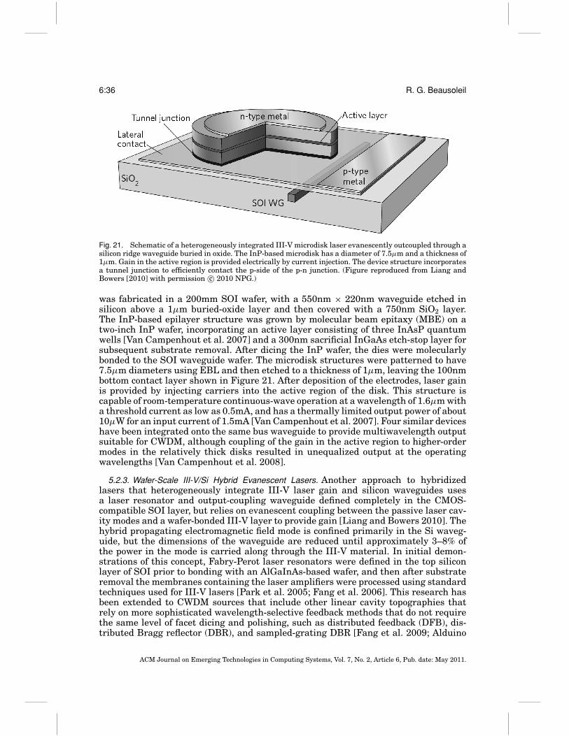
6:36 R. G. Beausoleil
Fig. 21. Schematic of a heterogeneously integrated III-V microdisk laser evanescently outcoupled through asilicon ridge waveguide buried in oxide. The InP-based microdisk has a diameter of 7.5μm and a thickness of1μm. Gain in the active region is provided electrically by current injection. The device structure incorporatesa tunnel junction to efficiently contact the p-side of the p-n junction. (Figure reproduced from Liang andBowers [2010] with permission c© 2010 NPG.)
was fabricated in a 200mm SOI wafer, with a 550nm × 220nm waveguide etched insilicon above a 1μm buried-oxide layer and then covered with a 750nm SiO2 layer.The InP-based epilayer structure was grown by molecular beam epitaxy (MBE) on atwo-inch InP wafer, incorporating an active layer consisting of three InAsP quantumwells [Van Campenhout et al. 2007] and a 300nm sacrificial InGaAs etch-stop layer forsubsequent substrate removal. After dicing the InP wafer, the dies were molecularlybonded to the SOI waveguide wafer. The microdisk structures were patterned to have7.5μm diameters using EBL and then etched to a thickness of 1μm, leaving the 100nmbottom contact layer shown in Figure 21. After deposition of the electrodes, laser gainis provided by injecting carriers into the active region of the disk. This structure iscapable of room-temperature continuous-wave operation at a wavelength of 1.6μm witha threshold current as low as 0.5mA, and has a thermally limited output power of about10μW for an input current of 1.5mA [Van Campenhout et al. 2007]. Four similar deviceshave been integrated onto the same bus waveguide to provide multiwavelength outputsuitable for CWDM, although coupling of the gain in the active region to higher-ordermodes in the relatively thick disks resulted in unequalized output at the operatingwavelengths [Van Campenhout et al. 2008].
5.2.3. Wafer-Scale III-V/Si Hybrid Evanescent Lasers. Another approach to hybridizedlasers that heterogeneously integrate III-V laser gain and silicon waveguides usesa laser resonator and output-coupling waveguide defined completely in the CMOS-compatible SOI layer, but relies on evanescent coupling between the passive laser cav-ity modes and a wafer-bonded III-V layer to provide gain [Liang and Bowers 2010]. Thehybrid propagating electromagnetic field mode is confined primarily in the Si waveg-uide, but the dimensions of the waveguide are reduced until approximately 3–8% ofthe power in the mode is carried along through the III-V material. In initial demon-strations of this concept, Fabry-Perot laser resonators were defined in the top siliconlayer of SOI prior to bonding with an AlGaInAs-based wafer, and then after substrateremoval the membranes containing the laser amplifiers were processed using standardtechniques used for III-V lasers [Park et al. 2005; Fang et al. 2006]. This research hasbeen extended to CWDM sources that include other linear cavity topographies thatrely on more sophisticated wavelength-selective feedback methods that do not requirethe same level of facet dicing and polishing, such as distributed feedback (DFB), dis-tributed Bragg reflector (DBR), and sampled-grating DBR [Fang et al. 2009; Alduino
ACM Journal on Emerging Technologies in Computing Systems, Vol. 7, No. 2, Article 6, Pub. date: May 2011.

Large-Scale Photonics for High-Performance Interconnects 6:37
Fig. 22. A hybrid integrated SOI/III-V microring laser. (a) A schematic of the laser structure showing the SOIring waveguide defining the laser resonator, the III-V gain region, and the SOI bus waveguide that transmitspower to tapered photodetectors. A transverse mode profile computed using the beam propagation methodis shown in the inset. (b) A microscope image of the integrated devices. (c) An SEM cross-sectional image ofthe structure near the coupler between the laser resonator and the bus waveguide. (Figure reproduced fromLiang et al. [2009b] with permission c© 2009 OSA.)
et al. 2010]. An alternate approach relied on a Si on-chip “racetrack” resonator laserthat in principle could be one of several such devices evanescently coupled to a commonbus waveguide for CWDM [Fang et al. 2007]. This laser demonstrated continuous-waveoutput at 1590nm with a threshold current of 175mA, an output power of 29mW, and amaximum operating temperature of 60C. Further reductions in the threshold currentrequire that the round-trip length of the racetrack cavity (which is greater than 2mm)be decreased significantly. For example, the hybrid microring laser structure shownin Figure 22 has a diameter of only 50μm—as well as very low optical and electricallosses—which allowed the device to be operated at a wavelength near 1530nm with athreshold current as low as 5.4mA at 10◦C [Liang et al. 2009b]. If high-temperatureperformance can be demonstrated for this device class, then ring diameters below 10μmshould enable threshold currents below 1mA, and the correspondingly small capaci-tance of the device should allow direct on-off-keying modulation rates above 10Gb/s[Liang and Bowers 2010]. As in the case of microdisk lasers [Van Campenhout et al.2008], several of these microring lasers could be coupled to the same waveguide bus,enabling highly integrated CWDM data transmission at low energy expenditures perbit. Initial demonstrations of mode-locked hybrid evanescent lasers based on Fabry-Perot cavities and generating 4ps pulses at 40GHz have been demonstrated with bothpassive and active/passive locking techniques [Koch et al. 2007], an important firststep toward compact DWDM laser sources. More complex external cavity quantum-well structures have demonstrated pulse durations as short as 60fs [Quarterman et al.2009], but it isn’t yet clear that these devices are candidates for large-scale integration.
5.3. Frequency-Comb Sources for DWDM
Although the potential for the large-scale integration of heterogeneous III-V/Si lasersis very promising, the case of ultra-high-bandwidth DWDM interconnects requires thatwe consider optical “power supplies” with channel counts approaching 64 (or even 128)
ACM Journal on Emerging Technologies in Computing Systems, Vol. 7, No. 2, Article 6, Pub. date: May 2011.

6:38 R. G. Beausoleil
and channel spacings of 40–120GHz, and optical output powers of multiple tens ofmilliwatts per channel so that we can link many network nodes to each other withoutrepeaters. Aggregating individual DFB lasers commonly used in the telecommunica-tions industry for computer network applications is probably infeasible: not only isthe cost prohibitive, but also the channel wavelength spacings would vary significantlywith time. The extensive monitoring and control required to maintain high data rateparallel links would also dramatically increase both system complexity and energyconsumption per received bit. Instead, as in the case of the optical parametric oscilla-tor source described above, laser systems that provide a comb of frequencies with fixedchannel spacing would allow the absolute wavelength of only one or two of the channelsto be monitored, and a modification of the temperature of the package (for example)would tune the entire comb.
5.3.1. Quantum-Dot Frequency-Comb Lasers. The Fabry-Perot (FP) resonator configura-tion, a linear cavity of length L formed by two mirrors, is ubiquitous in the laserindustry, and (given a sufficiently broadband gain medium) is capable of producinga large number of discrete wavelength channels separated from their nearest neigh-bors by the FSR frequency � fFSR = c/2ngL. For III-V laser amplifier materials withng ≈ 3, a laser with length L = 0.5mm has � fFSR ≈ 100GHz, compatible with the ITUO-band or C-band. Since temperature and other systematic effects cause only smallfractional changes in ngL, the FP comb spacing remains fixed even when the absolutewavelengths of the constituent channels shift significantly, allowing all channels to bestabilized and tracked simultaneously.
In contrast with the quantum-well gain materials described previously, quantum dotlaser amplifiers tend to provide broadband gain profiles due to significant variation inthe size of the dots. The gain spectrum of an individual quantum dot is typically smallerthan the FSR of a short FP cavity and the inhomogeneity of the size distribution of manydots grown using MBE can provide gain over a wavelength range of 40–60nm [Kovshet al. 2007], sufficient to support 50–100FP modes with 100GHz channel spacing. Thisrelatively large frequency separation also allows spectral hole burning in the gainmedium, which is an order of magnitude larger in quantum dots than quantum wells:dots that interact strongly with a particular longitudinal resonator mode generallyinteract weakly with other modes. This ensures that the relative intensity noise ofeach mode will be small enough to achieve low bit error rates (BER) under high speedmodulation of each channel [Gubenko et al. 2007]. The laser structure reported inWojcik et al. [2009] is grown by MBE on a GaAs substrate and incorporates 10 stackedplanes of InAs/InGaAs quantum dots in a 3μm×440nm waveguide structure fabricatedusing standard photolithography and etching techniques. The FP cavity is defined bycleaved facets, and the output of a typical device is shown in Figure 23. Here thefrequency channel spacing is 43GHz, and each of the 13 channels within 3dB of themost powerful channel is carrying at least 5mW. The relative intensity noise shownin the figure for one channel over the range 100kHz to 10GHz is characteristic of asingle-channel device, indicating that the gain coupling between adjacent channels isnegligibly small.
5.3.2. Externally Modulated Frequency Comb Sources. Another method that can be usedto generate a fixed comb of frequency channels is the external modulation of conven-tional III-V or fiber-optic laser sources. For example, the system shown schematically inFigure 24(a) relies on a dual-electrode Mach-Zehnder (amplitude and phase) modulator(DEMZM) to generate a broad and stable optical comb from a stand-alone continuous-wave laser source [Zhou et al. 2009a]. Experiments using this approach have demon-strated the output spectrum plotted in Figure 24(b) with 175 optical modes spanningover 3.5THz at 1550nm. The pulses emerging from the DEMZM are strongly frequency
ACM Journal on Emerging Technologies in Computing Systems, Vol. 7, No. 2, Article 6, Pub. date: May 2011.

Large-Scale Photonics for High-Performance Interconnects 6:39
Fig. 23. Electrically-pumped inhomogeneous quantum-dot gain regions can provide laser amplification overa broad spectrum, allowing a Fabry-Perot laser to generate a comb of frequencies with a channel spacing thatdepends only on the geometry of the resonator (left). The relative intensity noise of a given channel (right)shows that the coupling between adjacent channels is negligibly small. (Figure reproduced from Wojciket al. [2009] with permission c© 2009 SPIE.)
Fig. 24. Broadband frequency-comb generation for “optical power supply” of a DWDM interconnect system.(a) Schematic of a frequency-comb generation system comprised of a dual-electrode Mach-Zehnder modulatorand dispersion-decreasing fiber for pulse chirp reduction. (b) Plot of a comb of 175 frequency channels near1550nm spanning a 3.5 THz optical spectrum with nearly flat spectral phase. (Figure reproduced from Zhouet al. [2009] with permission c© 2009 by the authors.)
chirped, so dispersion engineering in both conventional optical fiber and dispersion-decreasing fiber was used to regularize the phase profile of the comb. This approachhas the advantage that the laser source can be chosen primarily for efficiency, outputpower, and spectral stability, and the active and dispersive elements could be mono-lithically integrated [Zhou et al. 2009a; Osgood et al. 2009]. However, the mode spacingis limited by the modulation frequency of the DEMZM, and the laser output (after ex-periencing the gain provided by the optical amplifier located between the two lengthsof fiber) must be large enough that ∼1W power consumption of the DEMZM does notsignificantly reduce the efficiency of the system.
6. PHOTONIC INTEGRATED CIRCUITS: INTEGRATION AND PACKAGING
Given that long-haul telecommunication has been the driver for much of the progressmade in the field of photonics over the last thirty years, the most common platformfor photonic integrated circuits (PICs) has been indium phosphide (InP) [Razavi 2002;
ACM Journal on Emerging Technologies in Computing Systems, Vol. 7, No. 2, Article 6, Pub. date: May 2011.

6:40 R. G. Beausoleil
Nagarajan et al. 2007]. Over the next decade, as bandwidth requirements for eachoptomechanical connector grow to 1Tb/s and beyond, distances demanding high-bandwidth interconnects shrink from meters to centimeters to millimeters, and thecost per optical component falls from US$100–1000 to US$0.001–1, silicon as a plat-form for PICs has become a strong contender [Gunn 2006; Liang and Bowers 2009;Hochberg and Baehr-Jones 2010]. Moving from InP to Si PICs could inspire a “Moore’sLaw” for photonics, and provide enormous leverage for dramatic improvements in in-tegrated optical technologies: annual sales for the global semiconductor industry havegrown to US$300B in 2010 [Gartner 2010], and historically investments in capitalequipment and R&D have been 10–15% and 15–20% of sales, respectively.
6.1. Integration: SOI as a PIC Platform
As discussed in Section 3, SOI is a promising PIC platform because it provides a1–3μm-thick low-index oxide substrate below a thin silicon top layer, providing anideal high-index-contrast environment for strongly confined optical waveguides. Muchof the progress in SOI PICs over the past decade has been made on individual de-vices or partially integrated optical systems built using EBL [Chen et al. 2009], butthere has been substantial recent progress in moving photonics to low-cost commod-ity CMOS-compatible processes. A collaboration of MIT, BAE Systems, Cornell, andLucent has demonstrated monolithically-integrated tunable optical filters, germaniumelectro-absorption modulators, and germanium p-i-n diode photodetectors using siliconwire waveguides within a full 150nm CMOS process flow [Beals et al. 2008]. Luxterademonstrated a 40Gb/s transceiver fabricated using a 130nm CMOS process in SOI[Gunn 2006; Pinguet et al. 2008], made possible by high-speed operation of electronicdriver circuits built in SOI as well as photonic devices with submicron feature sizesenabled by high-volume deep-UV photolithography. Intel demonstrated a WDM trans-mitter using rib waveguides on SOI [Liu et al. 2010a] that has eight channels capableof operating at 25Gb/s each, with integrated modulators and DEMUX/MUX basedon Mach-Zehnder interferometers (MZIs). The modulators were reversed-biased p-ndiodes operated in carrier depletion mode (discussed in Section 4), and the DEMUXand MUX used a cascaded asymmetric MZI design that allowed the entire device tohave single fiber input and output. A 5Gb/s single-channel transmitter based on anintegrated microring modulator flip-chip bonded to an electrical driver circuit was fab-ricated using a 130nm SOI CMOS process by Sun and Luxtera [Zheng et al. 2010], whoshowed that the entire device dissipated 400fJ/b at CMOS drive voltages.
The incorporation of germanium in silicon PICs complicates prospects for monolithicCMOS integration using SOI [Michel et al. 2010]. Previous demonstrations have reliedon a “front-end-of-line” (FEOL) approach, where after transistor fabrication SOI wafersare shuttled from a silicon foundry (which usually does not have the capacity to growpure germanium) to a Ge epitaxy facility to create photodetectors in the same layeras the Si electronics [Gunn 2006; Beals et al. 2008; Pinguet et al. 2008; Liow et al.2010; Michel et al. 2010]. Although in the near term this approach is likely to remaindominant for CMOS integration, in the long term a “back-end-of-line” (BEOL) process,where photodetectors in amorphous global interconnect layers could be connected to Sitransistors through metal vias, would be preferable [Michel et al. 2010]. Over the nextdecade, as wafer thinning and bonding technologies reaches mainstream semiconductorproducts, a 3D die-stacking approach [Black et al. 2006; Vantrease et al. 2008; Ahn et al.2009a] that connected separate electronic and photonic thinned wafers using through-silicon vias [ITRS 2009] would allow separate optimizations of large-scale integratedphotonics and electronics (even those based on entirely different substrates).
It remains to be seen whether the SiGe lasers discussed in Section 5.1.2 can operatewith multi-milliwatt output powers and ∼25% overall efficiency necessary for adoption
ACM Journal on Emerging Technologies in Computing Systems, Vol. 7, No. 2, Article 6, Pub. date: May 2011.

Large-Scale Photonics for High-Performance Interconnects 6:41
in high-bandwidth computer interconnects, but their prospects for wafer-scale integra-tion are similar to those of epitaxial Ge photodetectors on SOI. The III-V frequencycomb sources reviewed in Section 5.3 are designed to be used as stand-alone pack-ages, and will need to reach economies of scale (e.g., cost per unit power per channel)that are unprecedented for the III-V semiconductor industry that currently provideslasers for telecommunications. The hybrid III-V/Si lasers described in Section 5.2 areapproaching the complexity and level of integration of the most advanced III-V pho-tonic devices [Liang and Bowers 2009]. III-V epitaxial transfer of wafers as largeas 150mm in diameter [Liang et al. 2009a] and III-V die attachment to larger SOIwafers [Fedeli et al. 2008; Liu et al. 2010c] indicate the potential of this approachfor high-volume manufacturability. Intel’s recent demonstration of a CWDM 50-Gb/slink—incorporating hybrid lasers, low-voltage MZMs, passive silicon MUX and DE-MUX, and SiGe photodetectors—is a tour de force of integration performed in standardfabrication facilities [Alduino et al. 2010]. Despite this progress, it remains difficult topredict the long-term reliability, performance, device uniformity, and cost of the hybridapproach [Liang and Bowers 2010].
6.2. Trimming of Fabrication Imperfections in DWDM Systems
The feasibility of silicon as a platform for photonic integrated circuits requires thatdevices are fabricated uniformly at both the die and wafer scales [Hochberg and Baehr-Jones 2010]. Given spatial variations in feature sizes that are typical of CMOS ma-terials and fabrication processes, the impact on the performance characteristics ofphotonic devices is likely to be much greater than that of electronic devices [Selvarajaet al. 2010], particularly in the case of resonant WDM systems [Peng et al. 2010].For example, the resonance frequencies of microring resonators depend on the dimen-sions and effective refractive index of the waveguide forming the ring, and the simplediscretization of identical microrings at different locations within the mask reticle cancause significant variation in their passband locations. Variations in etch depths acrossa wafer that would have little impact on the operation of a transistor could cause asignificant shift in the resonance wavelengths of microrings formed from ridge waveg-uides. Batch-to-batch changes in the thickness of the top silicon of an SOI wafer—aswell as perturbations in this thickness across a single wafer—can cause problems evenif the etching is perfectly uniform.
To gain an appreciation for the magnitude of the problem for DWDM systems, con-sider a silicon wire waveguide operating at 1550nm that is 500nm wide and 250nmhigh on SOI. The effective group index of this waveguide is approximately ng ≈ 4,and the sensitivity of this index to small changes in the height of the waveguide isdn/dh ≈ 3.3 × 10⁻³nm−1 [Selvaraja et al. 2010]. From the discussion in Section 3.2.2,the shift in resonance m of a microring resonator formed from this wire waveguide is�λm = (λm/ng)(dn/dh)�h for a change in height �h, or equivalently
� fm
�h= c
ngλm
dndh
≈ 160GHz/nm. (19)
The worst-case 3-σ batch-to-batch plus intra-wafer edge-to-edge variation in the thick-ness of the top silicon layer of an 8-inch nominally 250nm Thick Unibond SOI waferavailable from Soitec [Soitec 2010] is ±5%, or ±12.5nm, corresponding to a variationin microring resonance frequency of � fm ≈ ±2THz. Recent measurements of micror-ing resonators operating at 1310nm and fabricated using 248nm photolithography areconsistent with a 3-σ edge-to-edge wafer thickness nonuniformity of 6nm peak-to-peak[Peng et al. 2010].
ACM Journal on Emerging Technologies in Computing Systems, Vol. 7, No. 2, Article 6, Pub. date: May 2011.

6:42 R. G. Beausoleil
Although as design rules for future lithographic technology nodes are adopted theproblem may not be as severe for large-footprint nonresonant silicon photonic devices[Selvaraja et al. 2010], it seems clear that some degree of “trimming” will be needed tobring resonant devices in DWDM systems into compliance with their design [Zortmanet al. 2010b]. One approach may be to use negative-thermooptic polymers as a claddingmaterial and/or in slot waveguides to athermalize the microrings, as described in Sec-tion 3.2.2. Alternatively, as part of postprocessing a PIC wafer, the characteristics ofindividual devices could be diagnosed [Cooper et al. 2010] and then corrected by expos-ing the polymer to UV light [Zhou et al. 2009b]. The most straightforward approachwould use a slow dynamic process to tune a monitored microring such as (for example)a liquid crystal cladding [Cort et al. 2009] or an integrated resistive heater [Watts et al.2009; Dong et al. 2010b; DeRose et al. 2010; Dong et al. 2010d; Zortman et al. 2010b].Integrated heaters have been demonstrated with tuning ranges as large as 32nm andresponse times as short as 1μs, at power cost of 4.4μW/GHz. Since dn/dT > 0 forsilicon, heating a microring will redshift (i.e., decrease) the resonance frequency of aring resonator. Alternatively, from Equation (12a), injecting carriers into a microringwill blueshift the ring. Using the DC shift data provided in [Xu et al. 2005] as a guide,the blue shift caused by charge injection for a 5-μm ring biased at 0.8V would dissipateapproximately 125μW/nm (or 1μW/GHz) at 1550nm [Ahn et al. 2009a]. It is clear thatthese corrections represent a nontrivial contribution to the total system power budgetif tighter control in the uniformity of fabricated rings can’t be achieved.
6.3. Packaging: Fiber-to-Waveguide Couplers
One of the most critical technologies that must be made cost effective before siliconphotonics can reach volume applications is the packaging of an interface between thesmall transverse mode of a high-index-contrast wire or rib waveguide (with typical area0.10–0.15μm2) and the larger transverse mode profile of a low-index-contrast waveg-uide such as an optical fiber (with typical area 50μm2). A practical solution—which mayrequire an optomechanical mount with either active [Zhang et al. 2010b] or passivealignment [Zimmermann et al. 2008] in addition to an optical mode convertor—shouldcompete with the cost of a typical data pin (∼US$0.01–0.02 per pin) on a standardelectronic IC package. In high-bandwidth applications requiring WDM, the opticalconnector/convertor cost may be amortized over the total number of data channels,resulting in a potentially significant reduction in packaging costs.
The adiabatically tapered spot-size convertor shown in Figure 25(a) first couples thehigh-index-contrast wire waveguide mode to a larger low-index-contrast waveguidebefore launching the mode into a laterally aligned butt-coupled (and possibly lensed)optical fiber [Almeida et al. 2003; Gunn 2006; Tsuchizawa et al. 2005]. The device in thefigure has a silicon taper with a length of at least 200μm and a tip that is typically lessthan 100nm wide. The polymer waveguide core has 3μm × 3μm transverse extent anda 3% index contrast. Coupling losses of ∼0.5dB have been reported for tapered fiberwith a mode size of 4.3μm, but this loss increases to 2.5dB for standard single-modefiber with a 9μm core [Tsuchizawa et al. 2005] (compared to an insertion loss of 20dBin the absence of a spot-size converter). In addition, the lateral alignment tolerance forthese couplers is generally less than 1μm for an additional loss of 1dB [Almeida et al.2003; Zimmermann et al. 2008].
Recent work on vertical mode conversion using high-index-contrast subwavelengthgratings in the configuration shown in Figure 25(b) has improved matching betweenwire waveguide and standard single-mode fiber with relaxed lateral alignment re-quirements [Van Laere et al. 2007a; Van Laere et al. 2007b; Roelkens et al. 2008;Zimmermann et al. 2008; Tang et al. 2010; Vermeulen et al. 2010]. Because of the highindex, the grating can be relatively short (∼25 periods) while providing a relatively
ACM Journal on Emerging Technologies in Computing Systems, Vol. 7, No. 2, Article 6, Pub. date: May 2011.

Large-Scale Photonics for High-Performance Interconnects 6:43
Fig. 25. Mode convertors coupling optical fibers to silicon wire waveguides. (a) A schematic of an adiabat-ically tapered spot-size converter in SOI. (b) Schematic of an adiabatically tapered subwavelength-gratingsingle-mode fiber-to-Si wire waveguide coupler in SOI. (Tsuchizawa et al. [2005] and Van Laere et al. [2007b],respectively, with permission c© 2005 IEEE.)
large wavelength band where coupling is efficient. The grating is designed to operatewith light incident at an angle of about 10◦ to minimize backreflection into the fiber. Asubwavelength grating coupler fabricated in SOI using a CMOS pilot line with 193nmDUV photolithography has been demonstrated with a peak coupling efficiency of about70% [Vermeulen et al. 2010] (similar to that reported in Pinguet et al. [2008]), a 3dBcoupling bandwidth of 80nm, and a 1dB misalignment tolerance of 2μm. The primaryadvantage of this approach over that of the end-coupled adiabatic taper is that lightcan be coupled onto the chip at any location that is convenient, which allows bothwafer-scale testing and packaging layout optimization.
Although a mechanically fixed connection between the cores of a single-mode waveg-uide and a single-mode fiber is the most direct solution to the packaging of an opticaldata “pin,” in some applications it may be economically more feasible to couple spatiallyseparated reference planes using a free-space optical interposer. Traditionally this hasbeen done using costly compound glass or plastic lenses with volumes on the order ofa few cubic millimeters, but recently a compact optic with strong focusing power hasbeen demonstrated that can be fabricated using planar CMOS fabrication technology[Fattal et al. 2010]. Following earlier work on high-index contrast subwavelength grat-ings (SWGs) for VCSELs [Huang et al. 2007, 2008], nonperiodic dielectric structures[Gerke and Piestun 2010] have been shown to shape optical phasefronts to steer or fo-cus incident light fields. Figure 26(a) is a microscope image of a mirror with a diameterof 150μm fabricated in 450nm of amorphous silicon on quartz. The mirror is formed ina single etch step from a grating with a fixed period of 670nm, with grooves that varyin width as a function of position. As shown in Figure 26(b), flat silicon cylindrical andspherical mirrors imaged an incident collimated beam with a focal length of 20mm,and more complicated groove patterns can focus light to diffraction-limited spots inboth mirror and lens configurations [Fattal et al. 2010].
7. CONCLUSION
Research on individual silicon photonic components has been so productive and rapidover the last decade that the primary uncertainty in predicting system-level perfor-mance has become the trade-offs which must be made to enable wafer-scale integration.If SOI is ultimately the preferred platform for integration, then both batch-to-batchand intra-wafer edge-to-edge variation of commercially available wafers must be moretightly controlled. Uniformity of devices after lithography and etching—particularlyresonant structures such as microring filters and modulators—will determine the
ACM Journal on Emerging Technologies in Computing Systems, Vol. 7, No. 2, Article 6, Pub. date: May 2011.
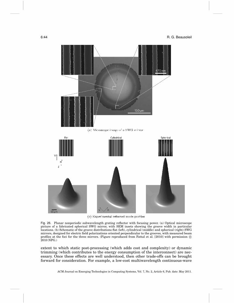
6:44 R. G. Beausoleil
Fig. 26. Planar nonperiodic subwavelength grating reflector with focusing power. (a) Optical microscopepicture of a fabricated spherical SWG mirror, with SEM insets showing the groove width in particularlocations. (b) Schematic of the groove distributions flat (left), cylindrical (middle) and spherical (right) SWGmirrors, designed for electric field polarizations oriented perpendicular to the grooves, with measured beamprofiles at the foci for the three mirrors. (Figure reproduced from Fattal et al. [2010] with permission c©2010 NPG.)
extent to which static post-processing (which adds cost and complexity) or dynamictrimming (which contributes to the energy consumption of the interconnect) are nec-essary. Once these effects are well understood, then other trade-offs can be broughtforward for consideration. For example, a low-cost multiwavelength continuous-wave
ACM Journal on Emerging Technologies in Computing Systems, Vol. 7, No. 2, Article 6, Pub. date: May 2011.
Large-Scale Photonics for High-Performance Interconnects 6:45
light source with a fixed channel spacing is vital as an “optical power supply” in aDWDM system. There are several promising candidates, either under active researchor commercially available in prototype form, but until a route to a low-cost high-volumeproduct can be identified it is difficult to specify the details of the on-chip DWDM com-ponents.
Therefore, although a strong case can be made using raw numbers and benchmarkmodels that future integrated circuits must inevitably rely on large-scale integratedphotonics for global-level interconnects, it is not yet clear exactly how this radically newtechnology will reach the market. To limit costs, supercomputers and data centers tendto rely on commodity components, which are unlikely to incorporate photonics withouta sustained collaboration of multinational semiconductor and information technologycompanies and government funding agencies. It is possible that a nearer-term real-ization of a monolithically-integrated PhASIC—such as an optically-enabled networkswitch—could have a substantial impact on high-performance computing. In eithercase, the Communications Technology Roadmap effort led by the MIT MicrophotonicsCenter [MIT 2010] should be encouraged and recognized as a critical step towardsbringing industry and academia together to establish a Moore’s Law for photonics.
ACKNOWLEDGMENTS
This work has benefited greatly from discussions and collaboration with J. Ahn, G. Astfalk, N. Binkert, J. E.Bowers, A. Davis, D. Fattal, M. Fiorentino, N. P. Jouppi, D. Liang, M. McLaren, T. Morris, N. Muralimanohar,C. M. Santori, R. S. Schreiber, M. R. T. Tan, D. Vantrease, S. Y. Wang, R. S. Williams, A. E. Willner, Q. Xu, andL. Zhang. Particular thanks are due to three anonymous referees who read the entire manuscript and mademany constructive comments that significantly improved the content and presentation of this material.
REFERENCES
AHN, D., YIN HONG, C., LIU, J., GIZIEWICZ, W., BEALS, M., KIMERLING, L. C., MICHEL, J., CHEN, J., AND KARTNER,F. X. 2007. High performance, waveguide integrated Ge photodetectors. Opt. Express 15, 7, 3916–3921.
AHN, J., FIORENTINO, M., BEAUSOLEIL, R. G., BINKERT, N., DAVIS, A., FATTAL, D., JOUPPI, N. P., MCLAREN, M., SANTORI,C. M., SCHREIBER, R. S., SPILLANE, S. M., VANTREASE, D., AND XU, Q. 2009a. Devices and architectures forphotonic chip-scale integration. Appl. Phys. A 95, 989–997.
AHN, J. H., BINKERT, N., DAVIS, A., MCLAREN, M., AND SCHREIBER, R. S. 2009b. HyperX: topology, routing,and packaging of efficient large-scale networks. In Proceedings of the Conference on High PerformanceComputing Networking, Storage and Analysis (SC). ACM, New York, NY, 1–11.
ALDUINO, A., LIAO, L., JONES, R., MORSE, M., KIM, B., LO, W.-Z., BASAK, J., KOCH, B., LIU, H.-F., RONG, H., SYSAK,M., KRAUSE, C., SABA, R., LAZAR, D., HORWITZ, L., BAR, R., LITSKI, S., LIU, A., SULLIVAN, K., DOSUNMU, O., NA,N., YIN, T., HAUBENSACK, F., WEI HSIEH, I., HECK, J., BEATTY, R., PARK, H., BOVINGTON, J., LEE, S., NGUYEN,H., AU, H., NGUYEN, K., MERANI, P., HAKAMI, M., AND PANICCIA, M. 2010. Demonstration of a high speed4-channel integrated silicon photonics WDM link with hybrid silicon lasers. In Proceedings of the OSATopical Meeting on Integrated Photonics Research (IPR). Optical Society of America, PDIWI5.
ALMEIDA, V. R., PANEPUCCI, R. R., AND LIPSON, M. 2003. Nanotaper for compact mode conversion. Opt.Lett. 28, 15, 1302–1304.
ASSEFA, S., XIA, F., AND VLASOV, Y. A. 2010. Reinventing germanium avalanche photodetector for nanophotonicon-chip optical interconnects. Nature 464, 7285, 80–84.
ASTFALK, G. 2009. Why optical data communications and why now? Appl. Phys. A 95, 933–940.BANERJEE, K. AND MEHROTRA, A. 2002. A power-optimal repeater insertion methodology for global interconnects
in nanometer designs. IEEE Trans. Electron. Dev. 49, 11, 2001–2007.BARRIOS, C. A. AND LIPSON, M. 2004. Modeling and analysis of high-speed electro-optic modulation in high
confinement silicon waveguides using metal-oxide-semiconductor configuration. J. Appl. Phys. 96, 11,6008–6015.
BATTEN, C., JOSHI, A., ORCUTT, J., KHILO, A., MOSS, B., HOLZWARTH, C., POPOVIC, M., LI, H., SMITH, H., HOYT,J., KARTNER, F., RAM, R., STOJANOVIC, V., AND ASANOVIC, K. 2009. Building many-core processor-to-DRAMnetworks with monolithic CMOS silicon photonics. IEEE Micro 29, 4, 8–21.
ACM Journal on Emerging Technologies in Computing Systems, Vol. 7, No. 2, Article 6, Pub. date: May 2011.
6:46 R. G. Beausoleil
BEALS, M., MICHEL, J., LIU, J. F., AHN, D. H., SPARACIN, D., SUN, R., HONG, C. Y., KIMERLING, L. C., POMERENE, A.,CAROTHERS, D., BEATTIE, J., KOPA, A., APSEL, A., RASRAS, M. S., GILL, D. M., PATEL, S. S., TU, K. Y., CHEN,Y. K., AND WHITE, A. E. 2008. Process flow innovations for photonic device integration in CMOS. Proc.Soc. Photo-Opt. Instrum. Eng. 6898, 1, 689804.
BEAUSOLEIL, R. G., AHN, J., BINKERT, N., DAVIS, A., FATTAL, D., FIORENTINO, M., JOUPPI, N. P., MCLAREN, M., SANTORI,C. M., SCHREIBER, R. S., SPILLANE, S. M., VANTREASE, D., AND XU, Q. 2008. A nanophotonic interconnect forhigh-performance many-core computation. IEEE LEOS Newslett. 22, 3, 15–22.
BEAUSOLEIL, R. G., KUEKES, P. J., SNIDER, G. S., WANG, S.-Y., AND WILLIAMS, R. S. 2008. Nanoelectronic andnanophotonic interconnect (Invited Paper). Proc. IEEE 96, 2, 230–247.
BENNER, A. 2009. Cost-effective optics: Enabling the exascale roadmap. In Proceedings of the 17th IEEESymposium on High Performance Interconnects (HOTI). 133–137.
BERGMAN, K. AND CARLONI, L. 2008. Power efficient photonic networks on-chip. Proc. Soc. Photo-Opt. Instrum.Eng. 6898, 689813.
BHATNAGAR, A., DEBAES, C., THIENPONT, H., AND MILLER, D. A. B. 2004. Receiverless detection schemes for opticalclock distribution. Proc. Soc. Photo-Opt. Instrum. Eng. 5359, 352–359.
BLACK, B., ANNAVARAM, M., BREKELBAUM, N., DEVALE, J., JIANG, L., LOH, G. H., MCCAULEY, D., MORROW, P.,NELSON, D. W., PANTUSO, D., REED, P., RUPLEY, J., SHANKAR, S., SHEN, J., AND WEBB, C. 2006. Die stacking(3D) microarchitecture. In Proceedings of the 39th Annual IEEE/ACM International Symposium onMicroarchitecture (MICRO-39). 469–479.
BLAND, A. S., KENDALL, R. A., KOTHE, D. B., ROGERS, J. H., AND SHIPMAN, G. M. 2009. Jaguar: The worlds mostpowerful computer. In Proceedings of the Cray User Group.
BLOCK, B. A., YOUNKIN, T. R., DAVIDS, P. S., RESHOTKO, M. R., CHANG, P., POLISHAK, B. M., HUANG, S., LUO, J.,AND JEN, A. K. Y. 2008. Electro-optic polymer cladding ring resonator modulators. Opt. Express 16, 22,18326–18333.
BOCK, P. J., CHEBEN, P., SCHMID, J. H., LAPOINTE, J., DELAGE, A., JANZ, S., AERS, G. C., XU, D.-X., DENSMORE, A.,AND HALL, T. J. 2010a. Subwavelength grating periodic structures in silicon-on-insulator: a new type ofmicrophotonic waveguide. Opt. Express 18, 19, 20251–20262.
BOCK, P. J., CHEBEN, P., SCHMID, J. H., LAPOINTE, J., DELAGE, A., XU, D.-X., JANZ, S., DENSMORE, A., AND HALL, T. J.2010b. Subwavelength grating crossings for silicon wire waveguides. Opt. Express 18, 15, 16146–16155.
BOGAERTS, W., DUMON, P., THOURHOUT, D. V., AND BAETS, R. 2007. Low-loss, low-cross-talk crossings for silicon-on-insulator nanophotonic waveguides. Opt. Lett. 32, 19, 2801–2803.
BOGAERTS, W., SELVARAJA, S., DUMON, P., BROUCKAERT, J., DE VOS, K., VAN THOURHOUT, D., AND BAETS, R. 2010.Silicon-on-insulator spectral filters fabricated with CMOS technology. IEEE J. Select. Topics QuantumElectron. 16, 1, 33–44.
BOYRAZ, O. AND JALALI, B. 2004. Demonstration of a silicon Raman laser. Opt. Express 12, 21, 5269–5273.CHEBEN, P., BOCK, P. J., SCHMID, J. H., LAPOINTE, J., JANZ, S., XU, D.-X., DENSMORE, A., DELAGE, A., LAMON-
TAGNE, B., AND HALL, T. J. 2010. Refractive index engineering with subwavelength gratings for efficientmicrophotonic couplers and planar waveguide multiplexers. Opt. Lett. 35, 15, 2526–2528.
CHEN, C., HARGIS, M., WOODALL, J., MELLOCH, M., REYNOLDS, J., YABLONOVITCH, E., AND WANG, W. 1999. GHzbandwidth GaAs light-emitting diodes. Appl. Phys. Lett. 74, 3140.
CHEN, L. AND LIPSON, M. 2009. Ultra-low capacitance and high speed germanium photodetectors on silicon.Opt. Express 17, 10, 7901–7906.
CHEN, L., PRESTON, K., MANIPATRUNI, S., AND LIPSON, M. 2009. Integrated GHz silicon photonic interconnectwith micrometer-scale modulators and detectors. Opt. Express 17, 17, 15248–15256.
CHU, T., FUJIOKA, N., AND ISHIZAKA, M. 2009. Compact, lower-power-consumption wavelength tunable laserfabricated with silicon photonic-wire waveguide micro-ring resonators. Opt. Express 17, 16, 14063–14068.
CLAPS, R., DIMITROPOULOS, D., HAN, Y., AND JALALI, B. 2002. Observation of Raman emission in silicon waveg-uides at 1.54μm. Opt. Express 10, 22, 1305–1313.
COLWELL, R. 2007. Computer Architecture Futures 2007. In Proceedings of the Federated Computing ResearchConference.
COOPER, M. L., GUPTA, G., PARK, J. S., SCHNEIDER, M. A., DIVLIANSKY, I. B., AND MOOKHERJEA, S. 2010. Quantitativeinfrared imaging of silicon-on-insulator microring resonators. Opt. Lett. 35, 5, 784–786.
CORT, W. D., BEECKMAN, J., JAMES, R., FERNANDEZ, F. A., BAETS, R., AND NEYTS, K. 2009. Tuning of silicon-on-insulator ring resonators with liquid crystal cladding using the longitudinal field component. Opt.Lett. 34, 13, 2054–2056.
D’ANDREA, D. 2009. CMOS photonics today & tomorrow. In Proceedings of the Optical Fiber CommunicationConference (OFC). Optical Society of America.
ACM Journal on Emerging Technologies in Computing Systems, Vol. 7, No. 2, Article 6, Pub. date: May 2011.

Large-Scale Photonics for High-Performance Interconnects 6:47
DEROSE, C. T., WATTS, M. R., TROTTER, D. C., LUCK, D. L., NIELSON, G. N., AND YOUNG, R. W. 2010. Siliconmicroring modulator with integrated heater and temperature sensor for thermal control. In Proceedingsof the Conference on Lasers and Electro-Optics (CLEO).
DOANY, F., SCHOW, C., BAKS, C., KUCHTA, D., PEPELJUGOSKI, P., SCHARES, L., BUDD, R., LIBSCH, F., DANGEL, R.,HORST, F., OFFREIN, B., AND KASH, J. 2009. 160 Gb/s bidirectional polymer-waveguide board-level opticalinterconnects using CMOS-based transceivers. IEEE Trans. Adv. Pack. 32, 2, 345–359.
DONG, P., LIAO, S., FENG, D., LIANG, H., ZHENG, D., SHAFIIHA, R., KUNG, C.-C., QIAN, W., LI, G., ZHENG, X.,KRISHNAMOORTHY, A. V., AND ASGHARI, M. 2009. Low vpp, ultralow-energy, compact, high-speed siliconelectro-optic modulator. Opt. Express 17, 25, 22484–22490.
DONG, P., LIAO, S., LIANG, H., QIAN, W., WANG, X., SHAFIIHA, R., FENG, D., LI, G., ZHENG, X., KRISHNAMOORTHY,A. V., AND ASGHARI, M. 2010a. High-speed and compact silicon modulator based on a racetrack resonatorwith a 1 V drive voltage. Opt. Lett. 35, 19, 3246–3248.
DONG, P., QIAN, W., LIANG, H., SHAFIIHA, R., FENG, N.-N., FENG, D., ZHENG, X., KRISHNAMOORTHY, A. V., AND
ASGHARI, M. 2010b. Low power and compact reconfigurable multiplexing devices based on silicon micror-ing resonators. Opt. Express 18, 10, 9852–9858.
DONG, P., QIAN, W., LIAO, S., LIANG, H., KUNG, C.-C., FENG, N.-N., SHAFIIHA, R., FONG, J., FENG, D., KRISHNAMOORTHY,A. V., AND ASGHARI, M. 2010c. Low loss shallow-ridge silicon waveguides. Opt. Express 18, 14, 14474–14479.
DONG, P., SHAFIIHA, R., LIAO, S., LIANG, H., FENG, N.-N., FENG, D., LI, G., ZHENG, X., KRISHNAMOORTHY, A. V., AND
ASGHARI, M. 2010d. Wavelength-tunable silicon microring modulator. Opt. Express 18, 11, 10941–10946.ESSIAMBRE, R.-J., FOSCHINI, G. J., KRAMER, G., AND WINZER, P. J. 2008. Capacity limits of information transport
in fiber-optic networks. Phys. Rev. Lett. 101, 16, 163901.FANG, A., SYSAK, M., KOCH, B., JONES, R., LIVELY, E., KUO, Y.-H., LIANG, D., RADAY, O., AND BOWERS, J.
2009. Single-wavelength silicon evanescent lasers. IEEE J. Select. Topics Quantum Electron. 15, 3,535–544.
FANG, A. W., JONES, R., PARK, H., COHEN, O., RADAY, O., PANICCIA, M. J., AND BOWERS, J. E. 2007. IntegratedAlGaInAs-silicon evanescent race track laser and photodetector. Opt. Express 15, 5, 2315–2322.
FANG, A. W., PARK, H., COHEN, O., JONES, R., PANICCIA, M. J., AND BOWERS, J. E. 2006. Electrically pumped hybridAlGaInAs-silicon evanescent laser. Opt. Express 14, 20, 9203–9210.
FANG, Q., PHANG, Y. T., TAN, C. W., LIOW, T.-Y., YU, M. B., LO, G. Q., AND KWONG, D. L. 2010. Multi-channelsilicon photonic receiver based on ring-resonators. Opt. Express 18, 13, 13510–13515.
FATTAL, D., FIORENTINO, M., TAN, M., HOUNG, D., WANG, S. Y., AND BEAUSOLEIL, R. G. 2008. Design of an efficientlight-emitting diode with 10 GHz modulation bandwidth. Appl. Phys. Lett. 93, 24, 243501.
FATTAL, D., LI, J., PENG, Z., FIORENTINO, M., AND BEAUSOLEIL, R. G. 2010. Flat dielectric grating reflectors withfocusing abilities. Nature Photon. 4, 7, 466–470.
FEDELI, J. M., CIOCCIO, L. D., MARRIS-MORINI, D., VIVIEN, L., OROBTCHOUK, R., ROJO-ROMEO, P., SEASSAL, C.,AND MANDORLO, F. 2008. Development of silicon photonics devices using microelectronic tools for theintegration on top of a CMOS wafer. Adv. Opt. Tech. 412518.
FENG, N.-N., DONG, P., ZHENG, D., LIAO, S., LIANG, H., SHAFIIHA, R., FENG, D., LI, G., CUNNINGHAM, J. E., KR-ISHNAMOORTHY, A. V., AND ASGHARI, M. 2010a. Vertical p-i-n germanium photodetector with high externalresponsivity integrated with large core Si waveguides. Opt. Express 18, 1, 96–101.
FENG, N.-N., LIAO, S., FENG, D., DONG, P., ZHENG, D., LIANG, H., SHAFIIHA, R., LI, G., CUNNINGHAM, J. E., KRISH-NAMOORTHY, A. V., AND ASGHARI, M. 2010b. High speed carrier-depletion modulators with 1.4 V-cm Vπ Lintegrated on 0.25μm silicon-on-insulator waveguides. Opt. Express 18, 8, 7994–7999.
FISCHER, U., ZINKE, T., KROPP, J.-R., ARNDT, F., AND PETERMANN, K. 1996. 0.1 dB/cm waveguide losses in single-mode SOI rib waveguides. IEEE Photon. Technol. Lett. 8, 5, 647–648.
FOSTER, M. A., SALEM, R., GERAGHTY, D. F., TURNER-FOSTER, A. C., LIPSON, M., AND GAETA, A. L. 2008. Silicon-chip-based ultrafast optical oscilloscope. Nature 456, 7218, 81–84.
FOSTER, M. A., SALEM, R., OKAWACHI, Y., TURNER-FOSTER, A. C., LIPSON, M., AND GAETA, A. L. 2009. Ultrafastwaveform compression using a time-domain telescope. Nature Photon. 3, 10, 581–585.
FOSTER, M. A., TURNER, A. C., SHARPING, J. E., SCHMIDT, B. S., LIPSON, M., AND GAETA, A. L. 2006. Broad-bandoptical parametric gain on a silicon photonic chip. Nature 441, 7096, 960–963.
FREY, B. J., LEVITON, D. B., AND MADISON, T. J. 2006. Temperature-dependent refractive index of silicon andgermanium. Proc. Soc. Photo-Opt. Instrum. Eng. 6273, 62732J, 1–10.
FUKUDA, H., YAMADA, K., TSUCHIZAWA, T., WATANABE, T., SHINOJIMA, H., AND ICHI ITABASHI, S. 2008. Polarizationrotator based on silicon wire waveguides. Opt. Express 16, 4, 2628–2635.
GARDES, F. Y., REED, G. T., MASHANOVICH, G. Z., AND PNG, C. E. 2008. Optical modulators in silicon photoniccircuits. In Silicon Photonics: The State of the Art, G. T. Reed (ed.), Wiley. 95–146.
ACM Journal on Emerging Technologies in Computing Systems, Vol. 7, No. 2, Article 6, Pub. date: May 2011.

6:48 R. G. Beausoleil
GARTNER. 2010. Press Release: “Gartner Says Worldwide Semiconductor Revenue to Grow 31.5 Percent in2010”. http://www.gartner.com/it/page.jsp?id=1430013.
GERKE, T. D. AND PIESTUN, R. 2010. Aperiodic volume optics. Nature Photon. 4, 3, 188–193.GILL, D., PATEL, S., RASRAS, M., TU, K.-Y., WHITE, A., CHEN, Y.-K., POMERENE, A., CAROTHERS, D., KAMOCSAI, R.,
HILL, C., AND BEATTIE, J. 2010. CMOS-compatible Si-ring-assisted Mach-Zehnder interferometer withinternal bandwidth equalization. IEEE J. Select. Topics Quantum Electron. 16, 1, 45–52.
GLICK, M. 2008. Optical interconnects in next generation data centers: An end to end view. In Proceedings ofthe 16th IEEE Symposium on High Performance Interconnects (HOTI). 178–181.
GNAN, M., THORNS, S., MACINTYRE, D., DE LA RUE, R., AND SOREL, M. 2008. Fabrication of low-loss photonicwires in silicon-on-insulator using hydrogen silsesquioxane electron-beam resist. Electron. Lett. 44, 2,115–116.
GNAUCK, A. H., TKACH, R. W., CHRAPLYVY, A. R., AND LI, T. 2008. High-capacity optical transmission systems.J. Lightwave Technol. 26, 9, 1032–1045.
GREEN, W. M., ROOKS, M. J., SEKARIC, L., AND VLASOV, Y. A. 2007. Ultra-compact, low RF power, 10 Gb/s siliconMach-Zehnder modulator. Opt. Express 15, 25, 17106–17113.
GREEN500. 2010. The Green500 List: Environmentally Responsible Supercomputing.http://www.green500.org.
GUBENKO, A., KRESTNIKOV, I., LIVSHTIS, D., MIKHRIN, S., KOVSH, A., WEST, L., BORNHOLDT, C., GROTE, N., AND
ZHUKOV, A. 2007. Error-free 10 Gbit/s transmission using individual Fabry-Perot modes of low-noisequantum-dot laser. Electron. Lett. 43, 25, 1430–1431.
GUHA, B., KYOTOKU, B. B. C., AND LIPSON, M. 2010. CMOS-compatible athermal silicon microring resonators.Opt. Express 18, 4, 3487–3493.
GUNN, C. 2006. CMOS photonics for high-speed interconnects. Micro, IEEE 26, 2, 58–66.HENNING, P. AND WHITE, A. 2009. Trailblazing with Roadrunner. Comput. Sci. Engin. 11, 4, 91–95.HO, R. 2003. On chip wires: Scaling and efficiency. Ph.D. thesis, Stanford University.HO, R., MAI, K., AND HOROWITZ, M. 2001. The future of wires. Proc. IEEE 89, 4, 490–504.HOCHBERG, M. AND BAEHR-JONES, T. 2010. Towards fabless silicon photonics. Nature Photon. 4, 8, 492–494.HP. 2010. Press Release: “Shell to use CeNSE for clearer picture of oil and gas reservoirs”.
http://www.hpl.hp.com/news/2009/oct-dec/cense.html.HU, J. AND MENYUK, C. R. 2009. Understanding leaky modes: slab waveguide revisited. Adv. Opt. Photon. 1, 1,
58–106.HUANG, M. C., ZHOU, Y., AND CHANG-HASNAIN, C. J. 2007. A surface-emitting laser incorporating a high-index-
contrast subwavelength grating. Nature Photon. 1, 2, 119–122.HUANG, M. C. Y., ZHOU, Y., AND CHANG-HASNAIN, C. J. 2008. Single mode high-contrast subwavelength grating
vertical cavity surface emitting lasers. Appl. Phys. Lett. 92, 17, 171108.INNOLUME. 2010. Innolume GmbH. http://www.innolume.com.ITRS. 2009. International Technology Roadmap for Semiconductors. http://www.itrs.net.JALALI, B. AND FATHPOUR, S. 2006. Silicon photonics. J. Lightwave Technol. 24, 12, 4600–4615.JIAO, Y., SHI, Y., DAI, D., AND HE, S. 2010. Accurate and efficient simulation for silicon-nanowire-based
multimode interference couplers with a 3D finite-element mode-propagation analysis. J. Opt. Soc.Amer. B 27, 9, 1813–1818.
JONES, R., RONG, H., LIU, A., FANG, A., PANICCIA, M., HAK, D., AND COHEN, O. 2005. Net continuous wave opticalgain in a low loss silicon-on-insulator waveguide by stimulated Raman scattering. Opt. Express 13, 2,519–525.
KANG, Y., LIU, H.-D., MORSE, M., PANICCIA, M. J., ZADKA, M., LITSKI, S., SARID, G., PAUCHARD, A., KUO, Y.-H.,CHEN, H.-W., ZAOUI, W. S., BOWERS, J. E., BELING, A., MCINTOSH, D. C., ZHENG, X., AND CAMPBELL, J. C. 2009.Monolithic germanium/silicon avalanche photodiodes with 340 GHz gain-bandwidth product. NaturePhoton. 3, 1, 59–63.
KIRMAN, N., KIRMAN, M., DOKANIA, R., MARTINEZ, J., APSEL, A., WATKINS, M., AND ALBONESI, D. 2007. On-chipoptical technology in future bus-based multicore designs. IEEE Micro 27, 1, 56–66.
KOCH, B. R., FANG, A. W., COHEN, O., AND BOWERS, J. E. 2007. Mode-locked silicon evanescent lasers. Opt.Express 15, 18, 11225–11233.
KOVSH, A., KRESTNIKOV, I., LIVSHITS, D., MIKHRIN, S., WEIMERT, J., AND ZHUKOV, A. 2007. Quantum dot laser with75nm broad spectrum of emission. Opt. Lett. 32, 7, 793–795.
KUMAR, R., ZYUBAN, V., AND TULLSEN, D. 2005. Interconnections in multi-core architectures: Understandingmechanisms, overheads and scaling. In Proceedings of the 32nd International Symposium on ComputerArchitecture. 408–419.
ACM Journal on Emerging Technologies in Computing Systems, Vol. 7, No. 2, Article 6, Pub. date: May 2011.

Large-Scale Photonics for High-Performance Interconnects 6:49
KUO, Y.-H., LEE, Y. K., GE, Y., REN, S., ROTH, J. E., KAMINS, T. I., MILLER, D. A. B., AND HARRIS, J. S. 2005. Strongquantum-confined Stark effect in germanium quantum-well structures on silicon. Nature 437, 7063,1334–1336.
LANL. 2010. High-Performance Computing: Raodrunner. See http://www.lanl.gov/roadrunner.LEE, B., BIBERMAN, A., CHAN, J., AND BERGMAN, K. 2010. High-performance modulators and switches for silicon
photonic networks-on-chip. IEEE J. Select. Topics Quantum Electron. 16, 1, 6–22.LEE, J.-M., KIM, D.-J., KIM, G.-H., KWON, O.-K., KIM, K.-J., AND KIM, G. 2008. Controlling temperature depen-
dence of silicon waveguide using slot structure. Opt. Express 16, 3, 1645–1652.LEUTHOLD, J., KOOS, C., AND FREUDE, W. 2010. Nonlinear silicon photonics. Nature Photon. 4, 8, 535–544.LEVY, J. S., GONDARENKO, A., FOSTER, M. A., TURNER-FOSTER, A. C., GAETA, A. L., AND LIPSON, M. 2010. CMOS-
compatible multiple-wavelength oscillator for on-chip optical interconnects. Nature Photon. 4, 1, 37–40.LI, J., FATTAL, D. A., AND BEAUSOLEIL, R. G. 2009. Crosstalk-free design for the intersection of two dielectric
waveguides. Opt. Express 17, 9, 7717–7724.LI, Y., ZHANG, L., SONG, M., ZHANG, B., YANG, J.-Y., BEAUSOLEIL, R. G., WILLNER, A. E., AND DAPKUS, P. D. 2008.
Coupled-ring-resonator-based silicon modulator for enhanced performance. Opt. Express 16, 17, 13342–13348.
LIANG, D. AND BOWERS, J. 2009. Photonic integration: Si or InP substrates? Electron. Lett. 45, 12, 578–581.LIANG, D. AND BOWERS, J. E. 2010. Recent progress in lasers on silicon. Nature Photon. 4, 8, 511–517.LIANG, D., BOWERS, J. E., OAKLEY, D. C., NAPOLEONE, A., CHAPMAN, D. C., CHEN, C.-L., JUODAWLKIS, P. W., AND
RADAY, O. 2009a. High-quality 150mm InP-to-silicon epitaxial transfer for silicon photonic integratedcircuits. Electrochem. Solid. Lett. 12, 4, H101–H104.
LIANG, D., FIORENTINO, M., OKUMURA, T., CHANG, H.-H., SPENCER, D. T., KUO, Y.-H., FANG, A. W., DAI, D.,BEAUSOLEIL, R. G., AND BOWERS, J. E. 2009b. Electrically-pumped compact hybrid silicon microring lasersfor optical interconnects. Opt. Express 17, 22, 20355–20364.
LIAO, L., LIU, A., BASAK, J., NGUYEN, H., PANICCIA, M., RUBIN, D., CHETRIT, Y., COHEN, R., AND IZHAKY, N. 2007.40 Gbit/s silicon optical modulator for highspeed applications. Electron. Lett. 43, 22.
LIOW, T.-Y., ANG, K.-W., FANG, Q., SONG, J.-F., XIONG, Y.-Z., YU, M.-B., LO, G.-Q., AND KWONG, D.-L. 2010.Silicon modulators and germanium photodetectors on SOI: Monolithic integration, compatibility, andperformance optimization. IEEE J. Select. Topics Quantum Electron. 16, 1, 307–315.
LIPSON, M. 2005. Guiding, modulating, and emitting light on silicon—challenges and opportunities. 23, 12,4222–4238.
LIPSON, M. 2009. Silicon photonics: the optical spice rack. Electron. Lett. 45, 12, 576–578.LIRA, H. L. R., MANIPATRUNI, S., AND LIPSON, M. 2009. Broadband hitless silicon electro-optic switch for on-chip
optical networks. Opt. Express 17, 25, 22271–22280.LITTLE, B., CHU, S., ABSIL, P., HRYNIEWICZ, J., JOHNSON, F., SEIFERTH, F., GILL, D., VAN, V., KING, O., AND TRAKALO,
M. 2004. Very high-order microring resonator filters for WDM applications. IEEE Photon. Technol.Lett. 16, 10, 2263–2265.
LIU, A., JONES, R., LIAO, L., SAMARA-RUBIO, D., RUBIN, D., COHEN, O., NICOLAESCU, R., AND PANICCIA, M. J. 2004a.A high-speed silicon optical modulator based on a metal-oxide-semiconductor capacitor. Nature 427,615–618.
LIU, A., LIAO, L., CHETRIT, Y., BASAK, J., NGUYEN, H., RUBIN, D., AND PANICCIA, M. 2010a. Wavelength divisionmultiplexing based photonic integrated circuits on silicon-on-insulator platform. IEEE J. Select. TopicsQuantum Electron. 16, 1, 23–32.
LIU, A., LIAO, L., RUBIN, D., NGUYEN, H., CIFTCIOGLU, B., CHETRIT, Y., IZHAKY, N., AND PANICCIA, M. 2007. High-speedoptical modulation based on carrier depletion in a silicon waveguide. Opt. Express 15, 2, 660–668.
LIU, A., RONG, H., PANICCIA, M., COHEN, O., AND HAK, D. 2004b. Net optical gain in a low loss silicon-on-insulatorwaveguide by stimulated Raman scattering. Opt. Express 12, 18, 4261–4268.
LIU, J., BEALS, M., POMERENE, A., BERNARDIS, S., SUN, R., CHENG, J., KIMERLING, L. C., AND MICHEL, J. 2008.Waveguide-integrated, ultralow-energy GeSi electro-absorption modulators. Nature Photon. 2, 7, 433–437.
LIU, J., SUN, X., CAMACHO-AGUILERA, R., KIMERLING, L. C., AND MICHEL, J. 2010b. Ge-on-Si laser operating atroom temperature. Opt. Lett. 35, 5, 679–681.
LIU, L., KUMAR, R., HUYBRECHTS, K., SPUESENS, T., ROELKENS, G., GELUK, E.-J., DE VRIES, T., REGRENY, P.,VAN THOURHOUT, D., BAETS, R., AND MORTHIER, G. 2010c. An ultra-small, low-power, all-optical flip-flopmemory on a silicon chip. Nature Photon. 4, 3, 182–187.
MANIPATRUNI, S., CHEN, L., AND LIPSON, M. 2010b. Ultra high bandwidth wdm using silicon microring modula-tors. Opt. Express 18, 16, 16858–16867.
ACM Journal on Emerging Technologies in Computing Systems, Vol. 7, No. 2, Article 6, Pub. date: May 2011.

6:50 R. G. Beausoleil
MANIPATRUNI, S., DOKANIA, R. K., SCHMIDT, B., SHERWOOD-DROZ, N., POITRAS, C. B., APSEL, A. B., AND LIPSON,M. 2008. Wide temperature range operation of micrometer-scale silicon electro-optic modulators. Opt.Lett. 33, 19, 2185–2187.
MANIPATRUNI, S., POITRAS, C. B., XU, Q., AND LIPSON, M. 2008. High-speed electro-optic control of the opticalquality factor of a silicon microcavity. Opt. Lett. 33, 15, 1644–1646.
MANIPATRUNI, S., PRESTON, K., CHEN, L., AND LIPSON, M. 2010. Ultra-low voltage, ultra-small mode volumesilicon microring modulator. Opt. Express 18, 17, 18235–18242.
MANIPATRUNI, S., XU, Q., AND LIPSON, M. 2007a. Pinip based high-speed high-extinction ratio micron-size siliconelectrooptic modulator. Opt. Express 15, 20, 13035–13042.
MANIPATRUNI, S., XU, Q., SCHMIDT, B., SHAKYA, J., AND LIPSON, M. 2007b. High speed carrier injection 18 Gb/ssilicon micro-ring electro-optic modulator. In Proceedings of the IEEE Lasers and Electro-Optics Society(LEOS) 20th Annual Meeting. 537–538.
MASHANOVICH, G. Z., REED, G. T., TIMOTIJEVIC, B. D., AND CHAN, S. P. 2008. Silicon photonic waveguides. InSilicon Photonics: The State of the Art, G. T. Reed (ed.). Wiley, 15–46.
MCINTYRE, R. 1966. Multiplication noise in uniform avalanche diodes. IEEE Trans. Electron Devices 13, 1,164–168.
MEINDL, J. D., DAVIS, J. A., ZARKESH-HA, P., PATEL, C. S., MARTIN, K. P., AND KOHL, P. A. 2002. Interconnectopportunities for gigascale integration. IBM J. Res. Dev. 46, 245.
MICHEL, J., LIU, J., AND KIMERLING, L. C. 2010. High-performance Ge-on-Si photodetectors. Nature Photon. 4, 8,527–534.
MILLER, D. 2000. Rationale and challenges for optical interconnects to electronic chips. Proc. IEEE 88, 6,728–749.
MILLER, D. 2009. Device requirements for optical interconnects to silicon chips. Proc. IEEE 97, 7, 1166–1185.MIT. 2010. MIT Microphotonics Center: Communications Technology Roadmap. See http://mphotonics
.mit.edu.MOORE, G. E. 1965. Cramming more components onto integrated circuits. Electron. 38, 114–117.MORICHETTI, F., CANCIAMILLA, A., FERRARI, C., TORREGIANI, M., MELLONI, A., AND MARTINELLI, M. 2010a. Roughness
induced backscattering in optical silicon waveguides. Phys. Rev. Lett. 104, 3, 033902.MORICHETTI, F., CANCIAMILLA, A., MARTINELLI, M., SAMARELLI, A., RUE, R. M. D. L., SOREL, M., AND MELLONI, A.
2010. Coherent backscattering in optical microring resonators. Appl. Phys. Lett. 96, 8, 081112.MORICHETTI, F., CANCIAMILLA, A., AND MELLONI, A. 2010b. Statistics of backscattering in optical waveguides.
Opt. Lett. 35, 11, 1777–1779.MORRIS, T. 2009. Breaking free of electrical constraints. Appl. Phys. A 95, 941–944.MULLER, D. A. 2005. A sound barrier for silicon? Nature Mater. 4, 9 (Sept.), 645–647.NAGARAJAN, R., KATO, M., PLEUMEEKERS, J., EVANS, P., LAMBERT, D., CHEN, A., DOMINIC, V., MATHUR, A., CHAVARKAR,
P., MISSEY, M., DENTAI, A., HURTT, S., BACK, J., MUTHIAH, R., MURTHY, S., SALVATORE, R., JOYNER, C., ROSSI,J., SCHNEIDER, R., ZIARI, M., TSAI, H.-S., BOSTAK, J., KAUFFMAN, M., PENNYPACKER, S., BUTRIE, T., REFFLE,M., MEHUYS, D., MITCHELL, M., NILSSON, A., GRUBB, S., KISH, F., AND WELCH, D. 2007. Large-scale photonicintegrated circuits for long-haul transmission and switching. J. Opt. Netw. 6, 2, 102–111.
NARAYAN, S. 2009. Supercomputers: past, present and the future. Crossroads 15, 4, 7–10.NAWROCKA, M. S., LIU, T., WANG, X., AND PANEPUCCI, R. R. 2006. Tunable silicon microring resonator with wide
free spectral range. Appl. Phys. Lett. 89, 7, 071110.NG, H.-Y., WANG, M. R., LI, D., WANG, X., MARTINEZ, J., PANEPUCCI, R. R., AND PATHAK, K. 2008. 4×4 wavelength-
reconfigurable photonic switch based on thermally tuned silicon microring resonators. Opt. Eng. 47,044601.
OFFREIN, B. AND PEPELJUGOSKI, P. 2009. Optics in supercomputers. In Proceedings of the 35th European Con-ference on Optical Communication (ECOC). 1–2.
OKAMOTO, K. 2006. Fundamentals of Optical Waveguides 2nd Ed. Academic Press.ORNL. 2010. National Center for Computational Sciences: Jaguar. http://www.nccs.gov/computing-
resources/jaguar.OSGOOD, R. M., PANOIU, N. C., DADAP, J. I., LIU, X., CHEN, X., HSIEH, I.-W., DULKEITH, E., GREEN, W. M., AND
VLASOV, Y. A. 2009. Engineering nonlinearities in nanoscale optical systems: physics and applications indispersion-engineered silicon nanophotonic wires. Adv. Opt. Photon. 1, 1, 162–235.
OWENS, J., DALLY, W., HO, R., JAYASIMHA, D., KECKLER, S., AND PEH, L.-S. 2007. Research challenges for on-chipinterconnection networks. IEEE Micro 27, 5, 96–108.
PALANIAPPAN, A. AND PALERMO, S. 2010. Power efficiency comparisons of interchip optical interconnect archi-tectures. IEEE Trans. Circuits Syst. II, Exp. Briefs 57, 5, 343–347.
ACM Journal on Emerging Technologies in Computing Systems, Vol. 7, No. 2, Article 6, Pub. date: May 2011.

Large-Scale Photonics for High-Performance Interconnects 6:51
PARK, H., FANG, A., KODAMA, S., AND BOWERS, J. 2005. Hybrid silicon evanescent laser fabricated with a siliconwaveguide and III-V offset quantum wells. Opt. Express 13, 23, 9460–9464.
PASSARO, V. AND DELL’OLIO, F. 2008. Scaling and optimization of MOS optical modulators in nanometer SOIwaveguides. IEEE Trans. Nanotechnology 7, 4, 401–408.
PENG, Z., FATTAL, D., FIORENTINO, M., AND BEAUSOLEIL, R. G. 2010. Fabrication variations in SOI microrings forDWDM networks. In Proceedings of the IEEE Photonics Society 7th International Conference on GroupIV Photonics (GFP). P1.19.
PEPELJUGOSKI, P. K., KASH, J. A., DOANY, F., KUCHTA, D. M., SCHARES, L., SCHOW, C., TAUBENBLATT, M., OFFREIN,B. J., AND BENNER, A. 2010. Low power and high density optical interconnects for future supercomputers.In Proceedings of the Optical Fiber Communication Conference (OFC). Optical Society of America.
PINGUET, T., ANALUI, B., MASINI, G., SADAGOPAN, V., AND GLOECKNER, S. 2008. 40-Gbps monolithically integratedtransceivers in CMOS photonics. Proc. Soc. Photo-Opt. Instrum. Eng. 6898, 689805.
POULTON, J., PALMER, R., FULLER, A., GREER, T., EYLES, J., DALLY, W., AND HOROWITZ, M. 2007. A 14-mW 6.25-Gb/stransceiver in 90-nm CMOS. IEEE J. Solid-State Circuits 42, 12, 2745–2757.
PRESTON, K., MANIPATRUNI, S., GONDARENKO, A., POITRAS, C. B., AND LIPSON, M. 2009. Deposited silicon high-speedintegratedelectro-optic modulator. Opt. Express 17, 7, 5118–5124.
QUARTERMAN, A. H., WILCOX, K. G., APOSTOLOPOULOS, V., MIHOUBI, Z., ELSMERE, S. P., FARRER, I., RITCHIE, D. A.,AND TROPPER, A. 2009. A passively mode-locked external-cavity semiconductor laser emitting 60-fs pulses.Nature Photon. 3, 12, 729–731.
RAGHUNATHAN, V., YE, W. N., HU, J., IZUHARA, T., MICHEL, J., AND KIMERLING, L. 2010. Athermal operation ofsilicon waveguides: spectral, second order and footprint dependencies. Opt. Express 18, 17, 17631–17639.
RAMASWAMI, R., SIVARAJAN, K., AND SASAKI, G. 2009. Optical Networks: A Practical Perspective. Morgan Kauf-mann Publishers.
RASIGADE, G., MARRIS-MORINI, D., VIVIEN, L., AND CASSAN, E. 2010. Performance evolutions of carrier depletionsilicon optical modulators: From p-n to p-i-p-i-n diodes. IEEE J. Select. Topics Quantum Electron. 16, 1,179–184.
RAZAVI, B. 2002. Design of Integrated Circuits for Optical Communications. McGraw-Hill, New York.RAZZARI, L., DUCHESNE, D., FERRERA, M., MORANDOTTI, R., CHU, S., LITTLE, B. E., AND MOSS, D. J. 2010. CMOS-
compatible integrated optical hyper-parametric oscillator. Nature Photon. 4, 1, 41–45.REED, G. T., MASHANOVICH, G., GARDES, F. Y., AND THOMSON, D. J. 2010. Silicon optical modulators. Nature
Photon. 4, 8, 518–526.ROELKENS, G., VERMEULEN, D., THOURHOUT, D. V., BAETS, R., BRISION, S., LYAN, P., GAUTIER, P., AND
FEDELI, J.-M. 2008. High efficiency diffractive grating couplers for interfacing a single mode opticalfiber with a nanophotonic silicon-on-insulator waveguide circuit. Appl. Phys. Lett. 92, 13, 131101.
RONG, H., JONES, R., LIU, A., COHEN, O., HAK, D., FANG, A., AND PANICCIA, M. 2005. A continuous-wave Ramansilicon laser. Nature 433, 7027, 725–728.
RONG, H., XU, S., KUO, Y.-H., SIH, V., COHEN, O., RADAY, O., AND PANICCIA, M. 2007. Low-threshold continuous-wave Raman silicon laser. Nature Photon. 1, 4, 232–237.
RONG, Y., GE, Y., HUO, Y., FIORENTINO, M., TAN, M., KAMINS, T., OCHALSKI, T., HUYET, G., AND HARRIS, J. 2010.Quantum-confined Stark effect in Ge/SiGe quantum wells on Si. IEEE J. Select. Topics Quantum Elec-tron. 16, 1, 85–92.
ROTH, J. E., FIDANER, O., SCHAEVITZ, R. K., KUO, Y.-H., KAMINS, T. I., HARRIS, J. S., AND MILLER, D. A. B. 2007.Optical modulator on silicon employing germanium quantum wells. Opt. Express 15, 5851–5859.
SACHER, W. D. AND POON, J. K. S. 2008. Dynamics of microring resonator modulators. Opt. Express 16, 20,15741–15753.
SELVARAJA, S., BOGAERTS, W., DUMON, P., VAN THOURHOUT, D., AND BAETS, R. 2010. Subnanometer linewidthuniformity in silicon nanophotonic waveguide devices using CMOS fabrication technology. IEEE J.Select. Topics Quantum Electron. 16, 1, 316–324.
SOITEC. 2010. SOI Products. http://www.soitec.com/en/products/soi-products.php.SOLJACIC, M., IBANESCU, M., JOHNSON, S. G., FINK, Y., AND JOANNOPOULOS, J. D. 2002. Optimal bistable switching
in nonlinear photonic crystals. Phys. Rev. E 66, 5, 055601.SOREF, R. 2006. The past, present, and future of silicon photonics. IEEE J. Select. Topics Quantum Electron. 12,
1678–1687.SOREF, R. AND BENNETT, B. 1987. Electrooptical effects in silicon. IEEE J. Quantum Electron. 23, 1, 123–129.SPECTOR, S., SORACE, C., GEIS, M., GREIN, M., YOON, J., LYSZCZARZ, T., IPPEN, E., AND KARTNER, F. 2010. Op-
eration and optimization of silicon-diode-based optical modulators. IEEE J. Select. Topics QuantumElectron. 16, 1, 165–172.
ACM Journal on Emerging Technologies in Computing Systems, Vol. 7, No. 2, Article 6, Pub. date: May 2011.

6:52 R. G. Beausoleil
SUN, X., LIU, J., KIMERLING, L., AND MICHEL, J. 2010. Toward a germanium laser for integrated silicon photonics.IEEE J. Select. Topics Quantum Electron. 16, 1, 124–131.
TAN, M., ROSENBERG, P., YEO, J.-S., MCLAREN, M., MATHAI, S., MORRIS, T., KUO, H. P., STRAZNICKY, J., JOUPPI,N., AND WANG, S.-Y. 2009a. A high-speed optical multidrop bus for computer interconnections. IEEEMicro 29, 4, 62–73.
TAN, M., ROSENBERG, P., YEO, J.-S., MCLAREN, M., MATHAI, S., MORRIS, T., KUO, H. P., STRAZNICKY, J., JOUPPI,N., AND WANG, S.-Y. 2009b. A high-speed optical multidrop bus for computer interconnections. Appl.Phys. A 95, 945–953.
TANG, Y., WANG, Z., WOSINSKI, L., WESTERGREN, U., AND HE, S. 2010. Highly efficient nonuniform grating couplerfor silicon-on-insulator nanophotonic circuits. Opt. Lett. 35, 8, 1290–1292.
TAO, S. H., FANG, Q., SONG, J. F., YU, M. B., LO, G. Q., AND KWONG, D. L. 2008. Cascade wide-angle Y-junction1×16 optical power splitter based on silicon wire waveguides on silicon-on-insulator. Opt. Express 16, 26,21456–21461.
TOP500. 2010. TOP500 supercomputing sites. http://www.top500.org.TSIA, K. K., FATHPOUR, S., AND JALALI, B. 2008. Electrical control of parametric processes in silicon waveguides.
Opt. Express 16, 13, 9838–9843.TSUCHIZAWA, T., YAMADA, K., FUKUDA, H., WATANABE, T., ICHI TAKAHASHI, J., TAKAHASHI, M., SHOJI, T., TAMECHIKA,
E., ITABASHI, S., AND MORITA, H. 2005. Microphotonics devices based on silicon microfabrication technology.IEEE J. Select. Topics Quantum Electron. 11, 1, 232–240.
UENUMA, M. AND MOOOKA, T. 2009. Temperature-independent silicon waveguide optical filter. Opt. Lett. 34, 5,599–601.
VAN CAMPENHOUT, J., LIU, L., ROJO ROMEO, P., VAN THOURHOUT, D., SEASSAL, C., REGRENY, P., CIOCCIO, L., FEDELI,J., AND BAETS, R. 2008. A compact SOI-integrated multiwavelength laser source based on cascaded InPmicrodisks. IEEE Photon. Technol. Lett. 20, 16, 1345–1347.
VAN CAMPENHOUT, J., ROMEO, P. R., REGRENY, P., SEASSAL, C., THOURHOUT, D. V., VERSTUYFT, S., CIOC-CIO, L. D., FEDELI, J.-M., LAGAHE, C., AND BAETS, R. 2007. Electrically pumped InP-based microdisklasers integrated with a nanophotonic silicon-on-insulator waveguide circuit. Opt. Express 15, 11,6744–6749.
VAN LAERE, F., CLAES, T., SCHRAUWEN, J., SCHEERLINCK, S., BOGAERTS, W., TAILLAERT, D., O’FAOLAIN, L.,VAN THOURHOUT, D., AND BAETS, R. 2007a. Compact focusing grating couplers for silicon-on-insulatorintegrated circuits. IEEE Photon. Technol. Lett. 19, 23, 1919–1921.
VAN LAERE, F., ROELKENS, G., AYRE, M., SCHRAUWEN, J., TAILLAERT, D., VAN THOURHOUT, D., KRAUSS, T., AND
BAETS, R. 2007b. Compact and highly efficient grating couplers between optical fiber and nanophotonicwaveguides. J. Lightwave Technol. 25, 1, 151–156.
VANTREASE, D., BINKERT, N., SCHREIBER, R., AND LIPASTI, M. H. 2009. Light speed arbitration and flow control fornanophotonic interconnects. In Proceedings of the 42nd Annual IEEE/ACM International Symposiumon Microarchitecture. ACM, 304–315.
VANTREASE, D., SCHREIBER, R., MONCHIERO, M., MCLAREN, M., JOUPPI, N. P., FIORENTINO, M., DAVIS, A.,BINKERT, N., BEAUSOLEIL, R. G., AND AHN, J. 2008. Corona: System implications of emerging nanopho-tonic technology. In Proceedings of the 35th International Symposium on Computer Architecture.153–164.
VERMEULEN, D., SELVARAJA, S., VERHEYEN, P., LEPAGE, G., BOGAERTS, W., ABSIL, P., THOURHOUT, D. V., AND ROELKENS,G. 2010. High-efficiency fiber-to-chip grating couplers realized using an advanced CMOS-compatiblesilicon-on-insulator platform. Opt. Express 18, 17, 18278–18283.
VIVIEN, L., OSMOND, J., FEDELI, J.-M., MARRIS-MORINI, D., CROZAT, P., DAMLENCOURT, J.-F., CASSAN, E., LECUNFF, Y.,AND LAVAL, S. 2009. 42 GHz p.i.n germanium photodetector integrated in a silicon-on-insulator waveguide.Opt. Express 17, 8, 6252–6257.
VIVIEN, L., ROUVIERE, M., FEDELI, J.-M., MARRIS-MORINI, D., DAMLENCOURT, J. F., MANGENEY, J., CROZAT, P.,MELHAOUI, L. E., CASSAN, E., ROUX, X. L., PASCAL, D., AND LAVAL, S. 2007. High speed and high responsiv-ity germanium photodetector integrated in a silicon-on-insulator microwaveguide. Opt. Express 15, 15,9843–9848.
WANG, J., LOH, W., CHUA, K., ZANG, H., XIONG, Y., TAN, S., YU, M., LEE, S., LO, G., AND KWONG, D. 2008. Low-voltage high-speed (18 GHz/V) evanescent-coupled thin-film-Ge lateral PIN photodetectors integratedon Si waveguide. IEEE Photo. Technol. Lett. 20, 17, 1485–1487.
WATTS, M., TROTTER, D., YOUNG, R., AND LENTINE, A. 2008a. Ultralow power silicon microdisk modulators andswitches. In Proceedings of the IEEE 5th International Conference on Group IV Photonics (GFP). 4–6.
WATTS, M., ZORTMAN, W., TROTTER, D., NIELSON, G., LUCK, D., AND YOUNG, R. 2009. Adiabatic resonant microrings(ARMs) with directly integrated thermal microphotonics. In Proceedings of the Conference on Lasers andElectro-Optics (CLEO). CPDB10.
ACM Journal on Emerging Technologies in Computing Systems, Vol. 7, No. 2, Article 6, Pub. date: May 2011.

Large-Scale Photonics for High-Performance Interconnects 6:53
WATTS, M., ZORTMAN, W., TROTTER, D., YOUNG, R., AND LENTINE, A. 2010. Low-voltage, compact, depletion-mode,silicon Mach-Zehnder modulator. IEEE J. Select. Topics Quantum Electron. 16, 1, 159–164.
WATTS, M. R., TROTTER, D. C., AND YOUNG, R. W. 2008b. Maximally confined high-speed second-order silicon mi-crodisk switches. In Proceedings of the Optical Fiber Communication Conference (OFC). Optical Societyof America, PDP14.
WOJCIK, G. L., YIN, D., KOVSH, A. R., GUBENKO, A. E., KRESTNIKOV, I. L., MIKHRIN, S. S., LIVSHITS, D. A., FATTAL,D. A., FIORENTINO, M., AND BEAUSOLEIL, R. G. 2009. A single comb laser source for short reach WDMinterconnects. Proc. Soc. Photo-Opt. Instrum. Eng. 7230, 723021.
XIAO, S., KHAN, M. H., SHEN, H., AND QI, M. 2007. A highly compact third-order silicon microring add-drop filterwith a very large free spectral range, a flat passband and a low delay dispersion. Opt. Express 15, 22,14765–14771.
XU, Q. 2009. Silicon dual-ring modulator. Opt. Express 17, 23, 20783–20793.XU, Q., FATTAL, D., AND BEAUSOLEIL, R. G. 2008. Silicon microring resonators with 1.5-μm radius. Opt. Ex-
press 16, 6, 4309–4315.XU, Q., MANIPATRUNI, S., SCHMIDT, B., SHAKYA, J., AND LIPSON, M. 2007. 12.5 Gbit/s carrier-injection-based silicon
micro-ring silicon modulators. Opt. Express 15, 2, 430–436.XU, Q., SCHMIDT, B., PRADHAN, S., AND LIPSON, M. 2005. Micrometre-scale silicon electro-optic modulator. Na-
ture 435, 7040, 325–327.XU, Q., SCHMIDT, B., SHAKYA, J., AND LIPSON, M. 2006. Cascaded silicon micro-ring modulators for WDM optical
interconnection. Opt. Express 14, 20, 9431–9435.XUE, J., GARG, A., CIFTCIOGLU, B., WANG, S., HU, J., SAVIDIS, I., JAIN, M., HUANG, M., WU, H., FRIEDMAN, E. G.,
WICKS, G. W., AND MOORE, D. 2008. An intra-chip free-space optical interconnect. In Proceedings of the3rd Workshop on Chip Multiprocessor Memory Systems and Interconnects.
YIN, T., COHEN, R., MORSE, M. M., SARID, G., CHETRIT, Y., RUBIN, D., AND PANICCIA, M. J. 2007. 31GHz Ge n-i-p waveguide photodetectors on silicon-on-insulator substrate. Opt. Express 15, 21,13965–13971.
YOO, S. 2009. Future prospects of silicon photonics in next generation communication and computing systems.Electron. Lett. 45, 12, 584–588.
YOUNG, I., MOHAMMED, E., LIAO, J., KERN, A., PALERMO, S., BLOCK, B., RESHOTKO, M., AND CHANG, P. 2010. Opticali/o technology for tera-scale computing. IEEE J. Solid-State Circuits 45, 1, 235–248.
YU, Z. AND FAN, S. 2009. Complete optical isolation created by indirect interband photonic transitions. NaturePhoton. 3, 2, 91–94.
YUE, Y., ZHANG, L., SONG, M., BEAUSOLEIL, R. G., AND WILLNER, A. E. 2009. Higher-order-mode assisted silicon-on-insulator 90 degree polarization rotator. Opt. Express 17, 23, 20694–20699.
ZARLINK. 2010. Zarlink Semiconductor. http://www.zarlink.com.ZHANG, L., LI, Y., SONG, M., BEAUSOLEIL, R. G., AND WILLNER, A. E. 2008a. Data quality dependencies in
microring-based DPSK transmitter and receiver. Opt. Express 16, 8, 5739–5745.ZHANG, L., LI, Y., SONG, M., YANG, J.-Y., BEAUSOLEIL, R. G., AND WILLNER, A. E. 2009. Silicon microring-based
signal modulation for chip-scale optical interconnection. Appl. Phys. A 95, 1089–1100.ZHANG, L., LI, Y., YANG, J.-Y., SONG, M., BEAUSOLEIL, R. G., AND WILLNER, A. E. 2010a. Silicon-based micror-
ing resonator modulators for intensity modulation. IEEE J. Select. Topics Quantum Electron. 16, 1,149–158.
ZHANG, L., SONG, M., WU, T., ZOU, L., BEAUSOLEIL, R. G., AND WILLNER, A. E. 2008a. Embedded ring resonatorsfor microphotonic applications. Opt. Lett. 33, 17, 1978–1980.
ZHANG, L., YANG, J.-Y., LI, Y., SONG, M., BEAUSOLEIL, R. G., AND WILLNER, A. E. 2008b. Monolithic modulatorand demodulator of differential quadrature phase-shift keying signals based on silicon microrings. Opt.Lett. 33, 13, 1428–1430.
ZHANG, Q. X., DU, Y., TAN, C. W., ZHANG, J., YU, M. B., YEOH, W. G., LO, G.-Q., AND KWONG, D.-L. 2010b. A siliconplatform with MEMS active alignment function and its potential application in Si-photonics packaging.IEEE J. Select. Topics Quantum Electron. 16, 1, 267–275.
ZHENG, X., LEXAU, J., LUO, Y., THACKER, H., PINGUET, T., MEKIS, A., LI, G., SHI, J., AMBERG, P., PINCKNEY, N., RAJ,K., HO, R., CUNNINGHAM, J. E., AND KRISHNAMOORTHY, A. V. 2010. Ultra-low-energy all-CMOS modulatorintegrated with driver. Opt. Express 18, 3, 3059–3070.
ZHOU, L., KASHIWAGI, K., OKAMOTO, K., SCOTT, R. P., FONTAINE, N. K., DING, D., AKELLA, V., AND YOO, S. J. B. 2009a.Towards athermal optically-interconnected computing system using slotted silicon microring resonatorsand RF-photonic comb generation. Appl. Phys. A 95, 1101–1109.
ZHOU, L., OKAMOTO, K., AND YOO, S. 2009b. Athermalizing and trimming of slotted silicon microring resonatorswith UV-sensitive PMMA upper-cladding. IEEE Photon. Technol. Lett. 21, 17, 1175–1177.
ACM Journal on Emerging Technologies in Computing Systems, Vol. 7, No. 2, Article 6, Pub. date: May 2011.

6:54 R. G. Beausoleil
ZHOU, L. AND POON, A. W. 2006. Silicon electro-optic modulators using p-i-n diodes embedded 10-micron-diameter microdisk resonators. Opt. Express 14, 15, 6851–6857.
ZHU, S., FANG, Q., YU, M. B., LO, G. Q., AND KWONG, D. L. 2009. Propagation losses in undoped and n-dopedpolycrystalline silicon wire waveguides. Opt. Express 17, 23, 20891–20899.
ZIMMERMANN, L., TEKIN, T., SCHROEDER, H., DUMON, P., AND BOGAERTS, W. 2008. How to bring nanophotonics toapplication—silicon photonics packaging. IEEE LEOS Newsl. 22, 6, 4–14.
ZORTMAN, W. A., TROTTER, D. C., AND WATTS, M. R. 2010a. Silicon photonics manufacturing. Opt. Express 18, 23,23598–23607.
ZORTMAN, W. A., WATTS, M. R., TROTTER, D. C., YOUNG, R. W., AND LENTINE, A. L. 2010b. Low-power high-speedsilicon microdisk modulators. In Proceedings of the Conference on Lasers and Electro-Optics (CLEO).
Received September 2010; revised January 2011; accepted January 2011
ACM Journal on Emerging Technologies in Computing Systems, Vol. 7, No. 2, Article 6, Pub. date: May 2011.