large-format, high-speed, x-ray pnccds combined with ... · accelerator cavities with a fundamental...
TRANSCRIPT

Submitted to NIM A 1 - 25
Large-Format, High-Speed, X-ray pnCCDs Combined with Electron and Ion Imaging Spectrometers in a Multipurpose Chamber for Experiments at 4th Generation Light Sources
Lothar Strüder a,c,e,h, Sascha Epp a, Daniel Rolles a, Robert Hartmann b, Peter Holl b, Gerhard Lutz b, Heike Soltau b, Rouven Eckart b, Christian Reich b, Klaus Heinzinger b, Christian Thamm b, Artem Rudenko a, Faton Krasniqi a, Kai-Uwe Kühnel i, Christian Bauer i, Claus-Dieter Schröter i, Robert Moshammer a,i, Simone Techert a,m, Danilo Miessner c,e, Matteo Porro c,e, Olaf Hälker c,e, Norbert Meidinger c,e, Nils Kimmel c,e, Robert Andritschke c,e, Florian Schopper c,e, Georg Wei-denspointner c,e, Alexander Ziegler c,e, Daniel Pietschner c,e, Sven Herrmann c,e, Ullrich Pietsch h, Albert Walenta h, Wolfram Leitenberger h, Christoph Bostedt f, Thomas Möller f, Daniela Rupp f, Marcus Adolph f, Heinz Graafsma g, Helmut Hirsemann g, Klaus Gärtner k, Rainer Richter d,e, Lutz Foucar a, Robert L. Shoeman l, Ilme Schlichting a,l, Joachim Ullrich a,i a Max Planck Advanced Study Group, Center for Free Electron Laser Science (CFEL), Notkestr.
85, D-22607 Hamburg, Germany b PNSensor GmbH, Römerstraße 28, D-80803 München, Germany c Max-Planck-Institut für extraterrestrische Physik, Giessenbachstraße, D-85741 Garching, Germany d Max-Planck-Institut für Physik, Föhringer Ring 6, D-80805 München, Germany e MPI Halbleiterlabor, Otto-Hahn-Ring 6, D-81739 München, Germany f Technische Universität Berlin, Institut für Optik und Atomare Physik, Hardenbergstraße 36, D-10623 Berlin, Germany g DESY, Notkestr.85, D-22607 Hamburg, Germany h University of Siegen, Emmy-Noether Campus, Walter Flex Str. 3, D-57068 Siegen, Germany i Max-Planck-Institut für Kernphysik, Saupfercheckweg 1, D-69117 Heidelberg, Germany k Weierstrass Institut, Berlin, Mohrenstr. 39, D-10117 Berlin, Germany l Max-Planck-Institut für medizinische Forschung, Jahnstr. 29, D-69120 Heidelberg, Germany m Max-Planck-Institut für biophysikalische Chemie, Am Fassberg 11, 37077 Göttingen, Germany

Submitted to NIM A 2 - 25
1. Abstract Fourth generation accelerator-based light sources, such as VUV and X-ray Free Electron Lasers (FEL), deliver ultra-brilliant (~1012-1013 photons per bunch) coherent radiation in femtosecond (~10 fs to 100 fs) pulses and, thus, require novel focal plane instrumentation in order to fully ex-ploit their unique capabilities. As an additional challenge for detection devices, existing (FLASH, Hamburg) and future FELs (LCLS, Menlo Park; SCSS, Hyogo and the European XFEL, Ham-burg) cover a broad range of photon energies from the EUV to the X-ray regime with significantly different bandwidths and pulse structures reaching up to MHz micro-bunch repetition rates. Moreover, hundreds up to trillions of fragment particles, ions, electrons or scattered photons can emerge when a single light flash impinges on matter with intensities up to 1022 W/cm2.
In order to meet these challenges, the Max Planck Advanced Study Group (ASG) within the Center for Free Electron Laser Science (CFEL) has designed the CFEL-ASG MultiPurpose (CAMP) chamber. It is equipped with specially developed photon and charged particle detection devices dedicated to cover large solid-angles. A variety of different targets are supported, such as atomic, (aligned) molecular and cluster jets, particle injectors for bio-samples or fixed target arrangements. CAMP houses 4π solid-angle ion and electron momentum imaging spectrometers (“reaction microscope”, REMI, or “velocity map imaging”, VMI) in a unique combination with nov-el, large-area, broadband (50 eV to 25 keV), high-dynamic-range, single-photon-counting and imaging X-ray detectors based on the pnCCDs.
This instrumentation allows a new class of coherent diffraction experiments in which both elec-tron and ion emission from the target may be simultaneously monitored. This permits the inves-tigation of dynamic processes in this new regime of ultra-intense, high-energy radiation – matter interaction. After an introduction into the salient features of the CAMP chamber and the proper-ties of the redesigned REMI/VMI spectrometers, the new 1024 x 1024 pixel format pnCCD imag-ing detector system will be described in detail. Results of tests of four smaller format (256 x 512) devices of identical performance, conducted at FLASH and BESSY, will be presented and the concept as well as the anticipated properties of the full, large-scale system will be elucidated. The data obtained at both radiation sources illustrate the unprecedented performance of the X-ray detectors, which have a voxel size of 75 x 75 x 450 µm3 and a typical read-out noise of 2.5 electrons (rms) at an operating temperature of -50oC. Keywords: pnCCD, parallel readout, full depletion, back illuminated, radiation hard, visible light, UV light and X-ray detection, CAMP chamber, reaction microscope, velocity map imaging, X-ray imaging, X-ray spectroscopy, free electron laser

Submitted to NIM A 3 - 25
I. Introduction Since the beginning of this decade, several laboratories worldwide have decided to build a new generation of extremely intense, coherent and short-pulsed VUV and X-ray light sources: the (X-ray) free electron lasers or (X-)FELs. These revolutionary machines deliver up to 1013 photons in 10 fs to 100 fs bursts, in small, parallel beams with an energy uncertainty of ΔE/E ~ 10-3. They thus reach peak brilliances up to nine orders of magnitude higher than those achieved at the most advanced third-generation synchrotrons. Due to the small source size, the beam can be focused down to submicron spots, giving light intensities in the focus of up to 1022 W/cm2. The first machine of this kind was the Free electron LASer at Hamburg, FLASH at DESY [1]. FLASH has been operational since 2005 and produces light at wavelengths between 6 nm and 40 nm (i.e., 30 eV up to 200 eV) and pulse durations of about 25 fs. The next large facility to come online and presently in its commissioning phase is the Linac Coherent Light Source (LCLS) at SLAC in Menlo Park. LCLS is designed to deliver X-rays from below 0.8 keV up to 8 keV at 100 fs pulse duration [2]. While their basic concepts are identical, the practical realization and the operational schemes of FLASH and LCLS are quite different. FLASH employs super-conducting accelerator cavities with a fundamental repetition rate of 5 Hz or 10 Hz and can optionally deliver up to 3000 (design value) micro-bunches per macro-pulse train, while LCLS will operate with conventional accelerator cavities at a constant repetition rate between 30 Hz and 120 Hz. In 2010, the SPring8 Compact SASE Source (SCSS) will be commissioned in Japan [3] with beam parameters similar to LCLS and a repetition rate of 60 Hz. Finally, in 2014, another new facility will be opened to the scientific public, the X-ray Free Electron Laser, the European XFEL, in Hamburg [4]. The European XFEL will have a photon bunch structure similar to the one at FLASH. Every 100 ms, 3000 photon pulses, equally spaced in time by 200 ns, will be generated. After 600 µs, there will be a pause of 99.4 ms, which is the cooling phase of the cryogenic su-per-conducting accelerator cavities. This means that on average 30,000 X-ray pulses will be de-livered per second, providing 250 times the mean luminosity of LCLS and about 300 times the total photon flux achieved at PETRA III at DESY, the most advanced synchrotron in this energy range. Accordingly, it is envisioned that major breakthroughs in different scientific disciplines ranging from physics and chemistry to material and life sciences will be achieved with these discovery machines. Foremost among them is the dream to follow the “making and breaking” of molecular bonds in real-time, i.e., to record a “molecular movie”. In biology, one hopes to obtain structural information with sub-nanometer resolution of materials beyond the scope of conventional crystal-lographic approaches. These include nano- or non-crystalline proteins, macromolecular assem-blies, viruses, and cells. If successful, this approach would allow another access to the structure of membrane proteins which constitute about 60% of all therapeutic drug targets and are notori-ously difficult to crystallize. In general, due to their high coherence, brilliance, and short pulse time properties, FELs allow structural information to be obtained as a function of time, which will allow research in the femtosecond time regime. Beyond applications in biology and chemistry, this research is expected to be of utmost importance for the understanding of strongly correlated or magnetic materials, of phase transitions in liquids and solids, of melting processes at surfaces or in the bulk, of electron dynamics in atoms and molecules, and of strongly correlated plasmas. While these new machines promise unprecedented scientific possibilities, their properties also pose extreme challenges to the experimental instrumentation. For example, in some cases, scattered photon images have to be recorded at up to 5 MHz frame readout rates or, in other cases, hundreds, thousands or even more electrons and ions have to be detected per shot. Be-yond the requirements with respect to the performance of the detectors themselves, petabytes of data are recorded and have to be analyzed within reasonable times. Moreover, fundamental sci-entific questions arise beyond the “mere” technological challenges when penetrating this true terra incognita of light-matter interaction, which is orders of magnitude away from our present

Submitted to NIM A 4 - 25
experience in energy density at the given photon energies. Thus, one of the decisive open ques-tions regarding coherent imaging of biomolecules in the gas phase is whether the objects can be imaged before they are destroyed in the super-intense light flash. Since each single shot image will be a 2 dimensional projection of a 3 dimensional object, it will be necessary to know or to calculate the relative orientation of the molecule for each single shot before calculating a 3 di-mensional reconstruction. In order to meet some of these challenges concerning the instrumentation and to explore the relevant many-particle dynamics in this uncharted territory, we have designed the CFEL-ASG Multipurpose (CAMP) chamber. Proposed at the end of 2007 and designed in 2008 after exten-sive discussions within the scientific community, this chamber was built, tested and operated in 2009. The CAMP chamber houses the world’s largest pnCCD chips. These detectors operate with a frame readout rate of up to 200 Hz and are thus fully capable of meeting the requirements at LCLS (up to 120 Hz) and SCSS (up to 60 Hz), as well as the 10 Hz macro-bunch operation scheme at FLASH or the European XFEL. The high-speed European XFEL and FLASH opera-tion at up to 5 MHz is expected to be coped with the recently proposed DePFET active pixel sensors and hybrid pixel detector arrays [5]. In addition, large-solid-angle momentum imaging spectrometers for emitted electrons and ions, which are commonly referred to as “reaction mi-croscopes” (REMI) [6] or “velocity map imaging” (VMI) systems [7], have been redesigned and upgraded in order to enable simultaneous operation with the pnCCDs and to accommodate the fact that hundreds or even thousands of electrons and ions are emitted per shot. This combina-tion of pnCCD photon detection with advanced charged-particle detection is expected to deliver detailed information on the interaction dynamics of intense VUV and X-ray FEL pulses with mat-ter, to help uncover and subsequently possibly modify the destruction mechanisms of bio-particles to be imaged, to find schemes to dynamically align molecules for different shots by in-specting their fragmentation and scattering patterns shot by shot, etc. Thus, we envision that the CAMP chamber will serve a broad community encompassing coher-ent X-ray scattering and lensless imaging in material science (CXI), single particle and biomole-cule imaging (SPB), femtosecond diffraction imaging experiments (FDE), X-ray photon correla-tion spectroscopy (XPC), high energy density matter (HED) research, atomic and molecular physics (AMO), science with small quantum systems (SQS), X-ray absorption spectroscopy (XAS) and many more research areas to come. The unique combination of cutting edge imaging detectors along with the multi-user capability of the design was impressively affirmed by the fact that about 30 % of all approved (first campaign until December 2009) and proposed (second campaign starting in March 2010) experiments at LCLS plan to make use of the CAMP chamber. Moreover, a partial copy of the CAMP setup is presently under development for the Japanese SCSS free electron laser and has been designed such that our pnCCD detector array including chambers C2 and C3 (see Figure 1) can be directly implemented. Experiments in Japan are planned to be performed in 2010. This paper describes the general concept of the CAMP chamber, the REMI/VMI setup and the X-ray imagers. Since the REMI and VMI concepts have been discussed previously [6], we will concentrate on the changes and improvements necessary to combine them, for the first time, with photon detection. We will then focus on the detailed description of the pnCCD detector con-cept and elucidate how the pnCCD will meet the performance requests put forward by the users of the CAMP chamber. We will discuss the physical limitations of the system in terms of readout speed, noise performance, quantum efficiency, dynamic range, charge handling capacity, the dynamics of the charge cloud expansion and long term stability. We will further report on rele-vant previous results based on experiments performed at the BESSY synchrotron and at the FLASH facility. In this experiments, pnCCDs with an identical geometry (voxel size: 75 × 75 × 450 µm3 with a format of 256 × 256 × 2) were tested at a wide range of energies (30 eV to 35

Submitted to NIM A 5 - 25
keV) and intensities and provide a basis for extrapolation to the anticipated performance of the pnCCD detectors in the full CAMP chamber. II. The CFEL-ASG Multipurpose (CAMP) chamber As outlined before, the CAMP setup is designed to achieve two major goals:
(i) To obtain the most complete data sets possible by momentum-resolved, large-solid-angle correlated detection of a large number of the electrons, ions and scattered or fluorescent photons emitted in each shot, similarly to the data collection strategies employed in high-energy physics experiments. This shall be achieved for different situations in which the FEL beam hits atoms, molecules, solids or plasmas or when optical alignment as well as pump lasers are fed in to allow for pump-probe experiments on aligned molecules.
(ii) To guarantee high flexibility in order to enable the execution of a large variety of experiments. The ion and electron spectrometers allow for (coincident) many-particle, ion and electron momentum spectroscopy, as well as for velocity map imaging in combination with various jet targets. These components can be readily removed and replaced by other devices, such as fixed target setups, particle injectors or high-resolution electron time-of-flight (TOF) spec-trometers. Moreover, as will be illustrated below, the photon imaging detectors can even be mounted on the side of the incoming beam for more efficient detection of back-reflected or fluorescence light.
II.1 General concept, layout and dimensions
Figure 1 depicts the complete CAMP setup including the support and the Helmholtz coils for generating the magnetic projection field for the electrons in the REMI. The FEL beam enters the chamber from the left and can exit towards a beam dump to the right. The device consists of four sections, C0 to C3. From left to right, it starts with a differential pumping stage (C0), which en-sures that the beamline vacuum requirements are met even for main chamber pressures up to 10-6 mbar as may be present for injection of dense target beams. The first main chamber (C1), which has the FEL-sample interaction point at its center, houses the REMI or VMI spectrometers in the vertical direction (see Figure 2a), and the jet-target, particle injectors or fixed-target setups. The first movable pnCCD detector array, pnCCD1, is located in the next large chamber (C2) whereas the second detector array, pnCCD2, is accommodated in C3 (see Figure 2b). C1 and C2 have a ∅ 400 mm clear bore along the laser beam direction, whereas C3 has a ∅ 250 mm clear bore.
The design base pressure in the whole chamber is typically around 10-8 mbar, but can be low-ered to 10-10 mbar if required for particular experiments. To be able to reach this ultra-high vacu-um range, flexible and easy-to-mount helicoflex gaskets are used for the 400 mm flanges. To allow for remote three-dimensional position and angular alignment, which is crucial for the prop-er operation of the pnCCDs, the whole chamber assembly is mounted on an inner support (greenish in Figure 1) which can be moved independently along the x, y and z directions by ±50 mm, ±50 mm, and ±150 mm, respectively, with respect to the main support (blue in Figure 1), which remains fixed. Thus, the target point can be adjusted exactly to the FEL beam. Thereafter, the center of pnCCD2, which is fixed within C3, can be aligned with respect to the FEL beam direction by rotating the whole assembly in the horizontal as well as vertical directions around a fixed pivotal point, each by an angle of about ±6° as depicted in Figure 1a. Since this pivotal point does not coincide with the target location for technical reasons, an iterative procedure with subsequent 3D and angular alignment actions may be necessary in some cases.

Submitted to NIM A 6 - 25
Figure 1a: Side-view and dimensions of the CAMP chamber, which consists of the four chamber sections C0 to C3. The FEL beam enters from the left and is focused onto the target at the interaction point at the center of C1. The whole chamber assembly can be remotely adjusted via translational motions of the inner support (greenish brown) along each of the three spatial directions and tilt motions along the vertical and horizontal angles around the pivotal point (see text). The base support (blue) remains fixed.
Figure 1b: Three-dimensional view of the CAMP chamber assembly visualizing the Helmholtz coils that generate a magnetic field of up to 70 Gauss for momen-tum imaging of electrons in the REMI. As an example of one hardware configuration, a supersonic jet target (at-oms, molecules, clusters) is illustrated entering from the left along the –y direction, with the jet dump on the oppo-site side. Large, removable flanges permit simple hard-ware exchanges.
The unique and new feature provided by the fully equipped endstation is the possibility to simul-taneously operate electron, ion and photon momentum imaging detectors as illustrated in cross sections through C1 in Figure 2a, as well as through C1-C3 in Figure 2b. Conically shaped elec-trodes around the interaction point allow for a free line of sight to the interaction point from all directions and generate homogeneous (REMI) or inhomogeneous (VMI) electric fields to extract ions and electrons into different directions towards two-dimensional position and time-resolved multi-channel detectors. In the standard configuration, photons are detected via two pnCCD de-tector arrays placed downstream of the interaction point as depicted in Figure 2b. In this figure, the REMI/VMI was removed for better illustration of the pnCCDs, and, as an example, a super-sonic jet source is shown in combination with a fed-in laser that allows aligning the target mole-cules. We would like to stress that the full REMI/VMI setup can be included in a way that is fully compatible with the full position maneuverability of the pnCCD system.
(a) (b)
Submitted to NIM A 7 - 25
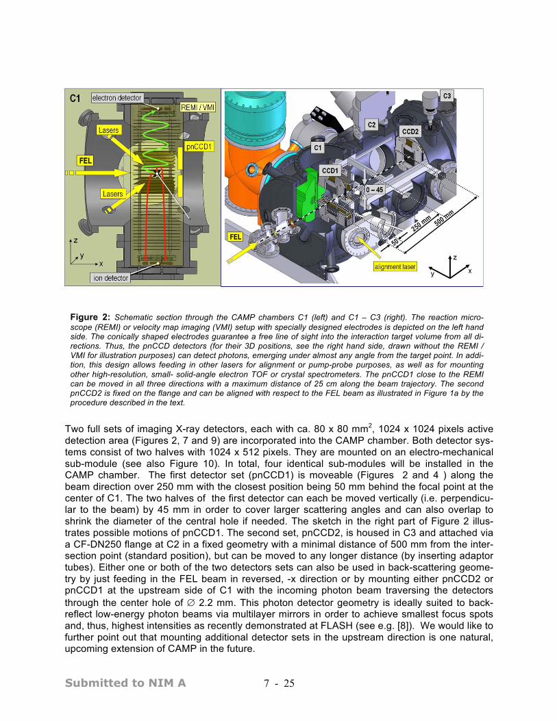
Figure 2: Schematic section through the CAMP chambers C1 (left) and C1 – C3 (right). The reaction micro-scope (REMI) or velocity map imaging (VMI) setup with specially designed electrodes is depicted on the left hand side. The conically shaped electrodes guarantee a free line of sight into the interaction target volume from all di-rections. Thus, the pnCCD detectors (for their 3D positions, see the right hand side, drawn without the REMI / VMI for illustration purposes) can detect photons, emerging under almost any angle from the target point. In addi-tion, this design allows feeding in other lasers for alignment or pump-probe purposes, as well as for mounting other high-resolution, small- solid-angle electron TOF or crystal spectrometers. The pnCCD1 close to the REMI can be moved in all three directions with a maximum distance of 25 cm along the beam trajectory. The second pnCCD2 is fixed on the flange and can be aligned with respect to the FEL beam as illustrated in Figure 1a by the procedure described in the text.
Two full sets of imaging X-ray detectors, each with ca. 80 x 80 mm2, 1024 x 1024 pixels active detection area (Figures 2, 7 and 9) are incorporated into the CAMP chamber. Both detector sys-tems consist of two halves with 1024 x 512 pixels. They are mounted on an electro-mechanical sub-module (see also Figure 10). In total, four identical sub-modules will be installed in the CAMP chamber. The first detector set (pnCCD1) is moveable (Figures 2 and 4 ) along the beam direction over 250 mm with the closest position being 50 mm behind the focal point at the center of C1. The two halves of the first detector can each be moved vertically (i.e. perpendicu-lar to the beam) by 45 mm in order to cover larger scattering angles and can also overlap to shrink the diameter of the central hole if needed. The sketch in the right part of Figure 2 illus-trates possible motions of pnCCD1. The second set, pnCCD2, is housed in C3 and attached via a CF-DN250 flange at C2 in a fixed geometry with a minimal distance of 500 mm from the inter-section point (standard position), but can be moved to any longer distance (by inserting adaptor tubes). Either one or both of the two detectors sets can also be used in back-scattering geome-try by just feeding in the FEL beam in reversed, -x direction or by mounting either pnCCD2 or pnCCD1 at the upstream side of C1 with the incoming photon beam traversing the detectors through the center hole of ∅ 2.2 mm. This photon detector geometry is ideally suited to back-reflect low-energy photon beams via multilayer mirrors in order to achieve smallest focus spots and, thus, highest intensities as recently demonstrated at FLASH (see e.g. [8]). We would like to further point out that mounting additional detector sets in the upstream direction is one natural, upcoming extension of CAMP in the future.

Submitted to NIM A 8 - 25
Figure 3: 3D model of the CAMP reac-tion microscope (a) and the velocity map imaging (b) spectrometers. The total length of both devices is 400 mm, and both are designed for ∅ 80 mm detec-tors. The conically shaped central elec-trodes are clearly visible. They provide a free line of sight for the pnCCDs over their complete active area and, at the same time, suppress stray light, which is , especially effective for the REMI ge-ometry. For the REMI typical voltages are a few V/cm. The VMI is operated at kV/cm for full solid-angle imaging of elec-trons up to 200 eV. With a magnetic field of up to 70 Gauss for the REMI, elec-trons emitted with energies of up to 2 keV into the most unfavourable direction, transverse to the electric extraction field, are confined to a spiral trajectory with a diameter of about 70 mm and, thus, are detected with a solid angle of 50 % of the full 4π steradiant. Multi-channel plate detectors are mounted at both ends and can be equipped with delay-line anodes or phosphor screen CCD camera readout (see text).
II.2 The target chamber and the reaction microscope setup
The REMI/VMI spectrometer (outer ∅ 90 mm for VMI and 135 mm for REMI, shown in yellow in left part of Figures 2), is mounted vertically in the standard setup such that it does not limit the motion of pnCCD1. This permits the mounting of different target jet devices along with lasers for alignment or pump-probe purposes. The middle part of each spectrometer consists of conically shaped, gold-plated aluminum electrodes that generate the homogeneous projecting (REMI, Figure 3a) or inhomogeneous imaging (VMI, Figure 3b) electric fields, respectively. Further out-side, two solid drift tubes (VMI) or equally spaced potential rings (REMI) guarantee a field-free drift region. The conical shape of the central electrodes within the solid angle covered by the pnCCD detectors allows unrestricted view into the scattering volume. At the same time, the cones excellently suppress scattered stray radiation emerging from outside the interaction center.
Since the operation principles of REMI/VMI spectrometers have been described extensively in the literature, only the salient features are briefly outlined in the present contribution. For the REMI configuration, illustrated in Figure 2a and 3a, the electric field forces all ions, independent of their initial momentum, onto parabolic trajectories (red lines in Figure 2a) and projects them onto the detector. The electric field, usually a few V/cm, can in most cases be adjusted such that all ions of interest are registered. Measuring the time-of-flight (TOF) and the hit position, the tra-jectory and, thus, the full three dimensional momentum vector of each individual ion can be re-constructed. Electrons are pushed towards the other hemisphere by the electric field but cannot be efficiently projected onto the detector with moderate fields. Even though their momenta are typically very similar to those of the ions, the electron energies are several thousand times larger, and accordingly, keV projection voltages would be required, leading to times-of flight of a few nanoseconds. This is too short to achieve reasonable momentum resolution along the extraction field direction. In a REMI, the dilemma is solved by maintaining a small electric field but confining the electrons’ transverse motion via an additional homogeneous (Helmholtz configuration, coil ∅ 160 cm) magnetic field (here up to 70 Gauss), oriented parallel to the electric field and forcing them onto spiral trajectories as sketched in Figure 2a (green line). Again, by measuring the TOF

Submitted to NIM A 9 - 25
and the hit position, the full initial momentum vector can be retrieved (for details, such as the at-tainable resolution, see [6]). Both detectors are equipped with either square or hexagonal delay line anodes (Roentdek HEX80 [9]) read out by an eight-channel, 2 GHz digitizer (Acquiris DC82x2) recording the complete wave form of the signal. It has been demonstrated recently at the SCSS test facility that up to 150 ions emerging from the interaction of a single EUV-FEL pulse with a single cluster could be analyzed, with their individual 3D momentum vectors [10] determined independently. In principle, the REMI allows for the coincident detection of momen-tum-resolved ions and electrons emerging from the same reaction. This feature has been used to explore sequential two-photon double ionization of Ne atoms in a kinematically complete ex-periment where two electrons and the ion have been detected in a triple coincidence [11]. Meanwhile, specially adapted REMIs have been successfully operated in many experiments at FLASH and the SCSS test facility [12-14] and the present design builds on this previous experi-ence.
Alternatively, if even more fragments are ejected per FEL shot, the delay line anode can be re-placed by a phosphor screen combined with a CCD camera readout, thus recording the image of electrons and/or ions without the magnetic field and applying non-homogeneous imaging voltag-es generated by the potential cones depicted in Figure 3b. In this “velocity map imaging” [7] mode, only two-dimensional (position) images are generated and the time information is usually lost due to short flight times of the electrons resulting from the large imaging electric fields of up to keV/cm. Still, under certain conditions and/or for low-energy electrons, three-dimensional im-ages can be retrieved (for details see [15]). Again, the applicability of this method at FELs has been proven recently at FLASH [16]. Since the standard VMI electrode configuration [7] had to be modified for our application, additional lenses are used to provide better space focusing [17].
In the standard REMI/VMI operation mode, two opposing CF-DN250 flanges in the horizontal direction in C1, perpendicular to the FEL beam, allow for installation of various targets, such as various supersonic jets (see Figure 1b and 2b), particle injectors, cluster or water droplet sources and their appropriate jet dumps. In this fully equipped setup, C1, C2, and C3 are pumped via TMPs (Turbo Molecular Pumps) mounted on four of the eight CF-DN150 flanges surrounding C2. By this means, utmost flexibility is provided for using the ports of C1 exclusively for experimental and user needs. C1 was kept as short as possible along the beam direction (400 mm) because of the relatively short X-ray focus lengths at some beamlines. Finally, the REMI/VMI setup is readily removable and other types of spectrometers (Thompson parabola, high-resolution electron TOF, magnetic bottle, high-resolution crystal or grating spectrometers, etc.) or fixed-target setups can be implemented instead. Supports in the chamber C1 allow mounting of apertures and fixed-target arrangements on breadboards. Various CF-DN38 ports allow the coupling of optical lasers from different directions, the mounting of various high-resolution VUV, X-ray or TOF electron spectrometers, beam monitors and much more. The ∅ 400 mm end-flange upstream contains additional ports for telescopes, laser injection, etc. Thin optical and mechanical blocking filters can be inserted in front of the detector pnCCD1 to prevent optical light and low-energy electrons from hitting the radiation sensitive windows of the X-ray imagers in the C2 and C3 chambers and to avoid chemical and mechanical contamination. The REMI magnetic field has the important side effect that it can effectively prevent electrons of up to 10 keV from hitting the pnCCDs, if required. Depending on the FEL beam energy and the target, the number of high-energy electrons produced might exceed that of scattered photons by orders of magnitude and therefore, could obscure many coherent imaging experiments. If de-sired, however, the magnetic field can be switched off and high-energy electrons can be detect-ed as well with the pnCCDs. Here, we would like to emphasize that the pnCCDs are also suita-ble for angle-resolved and energy-dispersive detection of high-energy electrons from at least one up to hundreds of keV. Due to the extreme granularity of the detector’s sensitive area, mil-lions of electrons emitted per shot can be recorded simultaneously, a fact that has not yet been realized by the broad scientific community. Electron detection can be of decisive advantage for many experiments, such as the investigation of plasmas generated either by optical or the X-ray

Submitted to NIM A 10 - 25
free electron laser pulses. Presently, the detection characteristics as a function of the electron energy of the pnCCDs is being investigated in a test setup and the results will be reported on in a separate, subsequent publication. III. pnCCDs for X-ray imaging spectroscopy The concept of the CAMP pn-junction charge coupled device is based on the pnCCDs [18] de-veloped for the X-ray satellite mission XMM-Newton [19]. XMM was launched in December 1999. Since then, the European Photon Imaging Camera with its pnCCD focal plane (EPICpn) has been delivering spectroscopic X-ray images of unprecedented quality. It is working reliably and stably, without the need for changing the operation conditions compared to the ground cali-brations. The maximum energy uncertainty at 6 keV has been only 2 eV over the past 10 years. In contrast to the well-known, more conventional metal-oxide-silicon based MOS CCDs, the pnCCDs are based on high-resistivity n-type silicon (typ. 5000 Ωcm) and a manufacturing pro-cess that makes use of both wafer surfaces for the sensor and electronics circuitry. This enables the full depletion of the entire silicon volume and, thus, makes use of the full depth as sensitive volume for the conversion of the incident X-rays into electron-hole pairs. Since all components of the sensor are built up with pn-junctions instead of MOS structures, the device is denoted pnCCD. A two-phase development program was started in spring 2007 in the framework of the CFEL-ASG to make specially designed pnCCD systems available to facilities where CFEL is scientifi-cally involved. Phase I comprises the commissioning of a high-speed 1024 × 1024 focal plane module in 2009 and phase II aims at providing a four times larger format module of 2048 × 2048 pixels to be operational in 2012/2013. III.1 pnCCD concept The pnCCD is fabricated on double-sided, polished, n-type 150 mm silicon wafers, typically 300 - 500 µm thick. The resistivity ρ of the bulk material varies between 3000 Ωcm and 6000 Ωcm to allow full depletion at bias voltages far below electrical breakdown. Full depletion is achieved by reverse-biased voltages applied to pn-junctions on the front and backside of the CCD, i.e. to the transfer registers (located at the “front side” of the detector) and to the photon entrance window (called “back contact” or radiation entrance window, see Fig. 5). By the choice of appropriate voltages, a potential minimum for electrons is created in the n-type silicon with an absolute min-imum at a depth of about 7 µm from the front surface. Incoming X-rays enter the pnCCD from the backside through the large-area, thin p+-implanted radiation entrance window. The energy
Figure 4: Artist’s view of the two pnCCD mount-ings. The two halves of the pnCCD on the left side (closest to the interaction point), CCD1, can be opened vertically by up to 90 mm, 45 mm each. Photons scattered under large angles can hence be detected, while the second (fixed) pnCCD2 records the X-rays under smaller angles. The dis-tance between the detectors can be changed by moving the CCD1 system up to 250 mm along the beam axis. Moreover, if needed, CCD2 can be placed at any distance larger than 550 mm away from the interaction zone by simply introducing fixed spacer tubes of the desired length.

Submitted to NIM A 11 - 25
needed to create an electron-hole pair in silicon is about 3.7 eV at a detector temperature of around -50oC. The electron-hole pairs, generated by the X-ray photons, are separated by the applied electric field of approximately 0.5 V/µm. The electrons drift to their potential minimum which is located inside an epitaxial layer of lower resistivity (approximately 40 Ωcm) on top of the bulk material. During photon integration time, the signals are stored in the potential wells of the pixels that are built up by three transfer registers with two different voltage levels applied. On command, the signal electrons are transferred with high-speed from the location where they have been stored towards the readout node. As with earlier pnCCDs, each transfer channel is terminated by an anode coupled to an on-chip amplifier (see Fig. 5), thus avoiding the time con-suming serialization (multiplexing) of a high-impedance signal. This concept was first proven with pnCCDs in 1990 in the test phase of the XMM mission [20]. The n+ anode, i.e. the arrival node of the signal charges at the end of a column, is connected to the p+ gate of an n-channel JFET, which is monolithically integrated on the pnCCD-chip (on-chip readout electronics in Fig. 5). Wire bonds connect the source of the JFET to a dedicated CAMEX preamplifier channel [28] in a source follower configuration (see Fig. 13).
Figure 5: Schematic view from the inside of a pnCCD. The X-rays enter the fully sensitive silicon volume of the pnCCD through the backside and generate electron-hole pairs at the location of their interaction with the silicon atoms. The signal electrons drift to the front side which has the pixel structure, while the holes are absorbed in the p+ back con-tact. In transfer direction a pixel is defined by three transfer registers with two different voltage levels (Φ1, Φ2 and Φ3). The signal charges are shifted in parallel to the end of the pixel column, where an on-chip amplifier serves as an input stage of a source follower. The lateral confinement of the signal charges, perpendicular to the shift direction, is guaran-teed by potential barriers created by fixed space charges introduced by ion implantation. The individual pnCCD column amplifier outputs are wire bonded in groups of 128 to an ASIC amplifier called CAMEX for further signal processing.
sensitive thickness (450 µm)
shift of sig-nal
charges
back contact
on – chip readout electronics
1 pixel (75 µm x 75 µm)
transfer regis-
ters

Submitted to NIM A 12 - 25
The extended sensitive depth of 450 µm enhances the quantum efficiency in the near infrared regime up to 1.1 µm wavelength as well as the X-ray region to about 50 % at 15 keV (see Fig. 6). The focal plane is cooled to approximately -50oC to minimize variations in pnCCD properties (noise, gain, and offset) and to improve long term stability of the devices.
Table 1: Experimental requirements for the 2-D detectors and current pnCCD properties
Parameter
2-D imager requirements for FLASH, LCLS, SCSS and XFEL requested by the user community
pnCCD properties
single photon resolu-tion
yes Yes
energy range 0.05 to 24 keV 0.05 to 25 keV signal rate/pixel/bunch 103 (105) 103 at 2 keV
charge handling ca-pacity ▬ approx. 5 x 10⁵ electrons per
pixel
quantum efficiency > 0.8 > 0.8 from 0.3 to 12 keV number of pixels, format 512 × 512 (min.) 1024 × 1024 and 2048 ×
2048
pixel size < 100 × 100 µm2 75 × 75 µm2 frame rate repetition rate
5 Hz to 120 Hz (except XFEL´s 5 MHz operation) continuous up to 200 Hz
externally triggerable ▬ yes
integrated center hole Ø 3 mm Ø 2.4 mm European XFEL burst mode 5 MHz (3 000) bunches not applicable
readout noise < 150 electrons 20 e- (low gain), 2 e- (high gain)
Figure 6: Quantum efficiency of the pnCCDs as a function of energy for a 450 µm thick pnCCD detector with different light blocking filters. The red curve shows the QE for an Al coating of 150 nm, which has a light attenua-tion of more than 106 in the visible region. The green curve corresponds to a 100 nm coating, the blue one to 50 nm of aluminum. The black curve denotes a configuration with only a thin SiO2 and Si3N4 passivation layer.. These layers are transparent for visi-ble light. For FLASH operation at 90 eV and 180 eV, the QE is 15 % with the 50 nm coating, while it is about 90 % in the LCLS energy range. At energies up to 10 keV, the QE is very close to 100 %.

Submitted to NIM A 13 - 25
III.2 pnCCD for free electron laser applications
We have proposed pnCCD modules as 2-dimensional X-ray sensitive focal plane detectors for use at 4th generation X-ray light sources. These imagers can measure either the X-ray intensity precisely or the X-ray energy in the case of single photons in one pixel. The relevant set of re-quired performance parameters for applications at the new X-ray laser sources are listed in Ta-ble 1. The main feature of the two-dimensional detector system is its capability to distinguish one photon from no photon over the full energy range and to supply a sufficiently large dynamic in-tensity range at a superior frame read-out repetition rate of 200 Hz. The measurement of up to one thousand 2 keV photons per pixel must be achieved with an intensity resolution of better than ± N , with N being the number of photons. Of course, every single shot has to be read out before the next 20 – 150 fs photon pulse hits the sample. In case of LCLS, this means that the frame time has to be shorter than 8 ms. Energy resolution as such was originally not desired ex-plicitly by the users. However, the possibility to separate the higher harmonics coming with the photon beam as well as the capability to measure fluorescence light and to discriminate against the elastically scattered photons was considered to be very helpful and essential for some of the anticipated experiments.
Figure 7: Schematic layout of the two halves of the 1024 x 1024 pnCCD sys-tem. Each half has a format of 512 x 1024 pixels of 75 µm x 75 µm size. The devices will be operated in a split frame mode, e.g. the upper (orange) pnCCD transfers the signal charges to the right (512 x 512) and to the left with the indi-cated device divider in the centre. There is no insensitive gap between the two 512 x 512 units. Both halves (1024 x 512) are operated independently. The on-chip amplifiers feed their signals in the CAMEX signal processors. Preamplification, bandwidth limitation, filtering, sample & hold multi-plexing and line driving is performed in the CAMEX chips. The CAMEX outputs are directly re-ceived by 16 ADCs located in the vicini-ty of the warm side of the DAQ electron-ics.
Submitted to NIM A 14 - 25
III. 3 Phase I: The 1024 ×1024 format
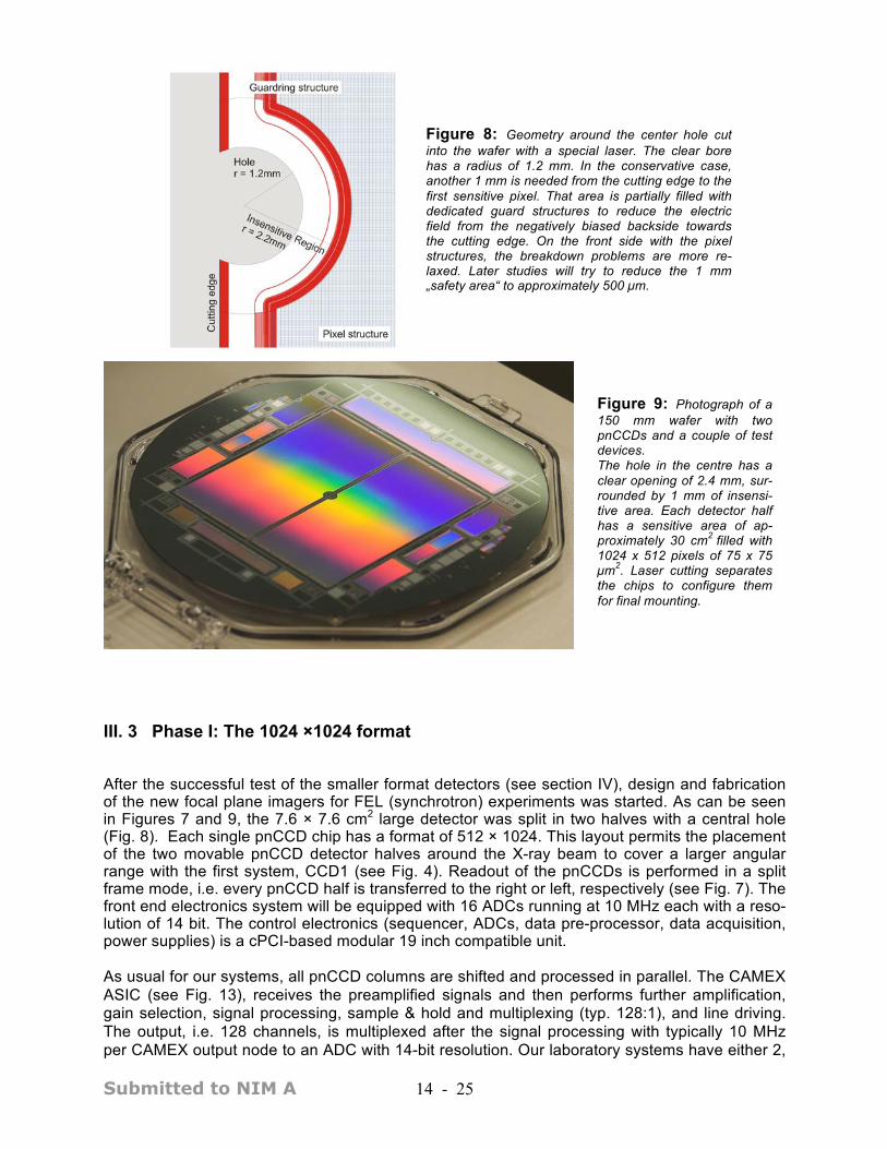
After the successful test of the smaller format detectors (see section IV), design and fabrication of the new focal plane imagers for FEL (synchrotron) experiments was started. As can be seen in Figures 7 and 9, the 7.6 × 7.6 cm2 large detector was split in two halves with a central hole (Fig. 8). Each single pnCCD chip has a format of 512 × 1024. This layout permits the placement of the two movable pnCCD detector halves around the X-ray beam to cover a larger angular range with the first system, CCD1 (see Fig. 4). Readout of the pnCCDs is performed in a split frame mode, i.e. every pnCCD half is transferred to the right or left, respectively (see Fig. 7). The front end electronics system will be equipped with 16 ADCs running at 10 MHz each with a reso-lution of 14 bit. The control electronics (sequencer, ADCs, data pre-processor, data acquisition, power supplies) is a cPCI-based modular 19 inch compatible unit. As usual for our systems, all pnCCD columns are shifted and processed in parallel. The CAMEX ASIC (see Fig. 13), receives the preamplified signals and then performs further amplification, gain selection, signal processing, sample & hold and multiplexing (typ. 128:1), and line driving. The output, i.e. 128 channels, is multiplexed after the signal processing with typically 10 MHz per CAMEX output node to an ADC with 14-bit resolution. Our laboratory systems have either 2,
Figure 9: Photograph of a 150 mm wafer with two pnCCDs and a couple of test devices. The hole in the centre has a clear opening of 2.4 mm, sur-rounded by 1 mm of insensi-tive area. Each detector half has a sensitive area of ap-proximately 30 cm2 filled with 1024 x 512 pixels of 75 x 75 µm2. Laser cutting separates the chips to configure them for final mounting.
Figure 8: Geometry around the center hole cut into the wafer with a special laser. The clear bore has a radius of 1.2 mm. In the conservative case, another 1 mm is needed from the cutting edge to the first sensitive pixel. That area is partially filled with dedicated guard structures to reduce the electric field from the negatively biased backside towards the cutting edge. On the front side with the pixel structures, the breakdown problems are more re-laxed. Later studies will try to reduce the 1 mm „safety area“ to approximately 500 µm.

Submitted to NIM A 15 - 25
4 or 8 output nodes. The digitized data are transferred to a computer through four optical 2.5 GHz links. The pnCCD data acquisition system can be upgraded to n × 4 output nodes. Every 4-channel ADC unit is housed in a 19 inch rack. The pnCCD system runs on a LINUX-based platform. Da-ta reduction can be performed with the help of an FPGA (Field Programmable Gate Array) lo-cated on the ADC motherboard. Gain correction, offset correction, common mode rejection, etc. are performed immediately after digitization. The final data analysis is done offline by the user, as the type of data analysis varies extensively for the different experiments. Data compression can be implemented in an FPGA directly behind the ADC.
The measurements shown in section 5 have been performed with an identical pnCCD system except for the format being 2 x 2562 instead of 10242. In the LCLS test case, the two pnCCD systems produce 2 x 10⁶ (2 cameras of 106 pixels each) x 120 (frames per second) x 2 (2 byte amplitude resolution) byte per second, i.e. almost 0.5 GByte of data per second, which trans-lates to 40 TByte per day. III. 4 Phase II: The 2048 × 2048 format Experimenters have requested larger fields of view and a smaller center hole, while retaining the flexibility of translating the detector halves. The ultimate reduction of the insensitive areas at the edges will be the aim of an upcoming technological study. The preliminary design and layout of a large-format subsystem (1024 x 1024 as shown in Fig. 11a) is already in progress and we plan to start the production in 2010 after the first feedback from the Phase I system has been re-ceived. Figure 11b shows the basic geometrical arrangement of the 4 Megapixel X-ray camera. It is composed of 4 identical subsystems which are joined together as shown below. The full sys-tem will have a sensitive area of 236 cm2 with approximately 0.8 % of insensitive area along the joints of the four detectors. The physical parameters of the Phase II system, such as noise, quantum efficiency, pixel size, charge handling capacity, energy range, etc., are identical to those of the Phase I system. Since the maximum number of transfers per CCD is 1024 instead of the 512 of the Phase I system, the readout of the Phase II pnCCD must be accelerated mod-erately to cope with the 120 Hz frame rate of LCLS.
Figure 10: Mechanical study of one of the movable halves of the detector system (sub-module). The pnCCD is the grey part in the center of the bottom layer, the CAMEX chips can be seen at the sides. They are wire bonded column-wise to the CAMEX chips located on the lower ceramic board. As the pnCCD is back-illuminated, the radiation of the EUROPEAN XFEL will hit the detector from the bottom. The upper board contains filter components for the DC power supplies as well as control logic and line drivers. The lower part containing the CCD and CAMEX chips is kept at a tem-perature between -50oC and room tempera-ture.
pnCCD

Submitted to NIM A 16 - 25
Correspondingly, the readout and data acquisition electronics will be upgraded to cope with the data rate of 2 GByte per second. In total, 64 ADCs will be needed to process the data in real-time. The processing time for one pixel has to be shorter than 7 µs. This translates to a CAMEX analog multiplexing (64:1) speed of approximately 10 MHz which is already achieved with to-day’s systems. III. 5 Charge spread in silicon detectors X-rays below 30 keV interacting with silicon deposit their energy predominantly through photoe-lectric absorption. Other processes like Compton scattering can be safely neglected. If the ener-gy of the incident X-ray is above 1.83 keV, the most probable process is K-shell ionization. In this case, the excess energy above the K-ionization level is transferred as kinetic energy to the outgoing electron, which then interacts with electrons in the same or neighboring silicon atoms. As the primary silicon atom is excited due to the missing K-shell electron, it relaxes either through the emission of a 1.74 keV photon or via the ejection of an Auger electron of about 1.55 keV, both of which deposit their energies in close vicinity. The size of the charge cloud as a func-
Figure 11: Next generation pnCCD device. (a) A monolithic 1024 x 1024 detector with 16 ADC ports is shown. pnCCD systems of this type can be put together on the three clear sides. According to the needs of the experi-ments, the devices can be fabricated with pixel sizes from 36 µm up to 100 µm. (b) A full 2048 x 2048 focal plane module is shown. It contains less than 1 % of insensitive gaps, and a total area of 240 cm2 can be read out in less than 8 ms.
(a) (b)

Submitted to NIM A 17 - 25
tion of the incident energy was approximated by H. J. Fitting et al. [22] to be Rel ~ ρ-0.8 E1.3el (Rel
is the radius of the electron range, ρ the density of the absorber material, and Eel the electron energy). This approximation [20] is reasonably good for energies well above the K-edge of the material. In the case of 4 keV incident X-rays, the charge cloud radius is on the order of 300 nm for back-illuminated pnCCDs. In a detector with a depleted volume depth of 500 µm and bias voltages around -200 V, electrons need about 5 ns to reach the potential minimum on the front side. During this time, electrostatic repulsion and diffusion widen the electron distribution to ap-proximately 7 µm (rms). As X-rays with energies below 4 keV are absorbed within 10 µm, i.e. close to the entrance (back-) side, the generated holes are more rapidly taken out through the negatively biased back contact. In cases where many X-rays, e.g. several thousands, hit the de-tector at the same time and position, the individual X-rays will be absorbed according to the 1/e attenuation law in point-like interactions along a line with individual but heavily overlapping charge spheres. For energies below 4 keV the length of such an “X-ray track” in silicon will be up to 10 µm long and the local charge clouds of the individual X-rays get mixed, leading to a charge “tube” with high charge densities of electrons and holes. Then, in a first step, the electric field of the detector removes only the outer skin of charges of the plasma while the inner part stays neu-tral but highly conductive – and expands further by diffusion. This is why a cloud with a high density of electrons expands more than extrapolated from low densities. We have started a project to calculate the time-dependent charge cloud expansion and are de-veloping a three dimensional device simulator solving the Poisson and continuity equations with a finite volume method on the basis of the given pnCCD geometry, under realistic operating conditions and doping concentrations. In this calculation, up to 800,000 electrons were homoge-neously deposited in a sphere of 10 µm diameter with the outer radius 2 µm above the backside of the depleted volume. The electrons were exposed to the internal electrical fields of the detec-tor. In Figure 12, the expanded electron distribution is shown after 1.3 ns in one quarter of a full pixel (75 x 75 x 150 µm3) with a footprint of 37.5 x 37.5 µm2. For technical reasons, it was not possible to simulate a larger volume with the required number of discrete elements. Moreover, we have assumed Neumann´s boundary conditions at all vertical faces of the pixels. This artifi-cially confines the signal charges inside the pixel as it assumes an infinite array of pixels and clouds. Under these conditions and with the approximations mentioned, the width of the charge cloud upon arrival in the potential minimum is on the order of half the pixel size. In the future, these model calculations will be further developed (e.g. enlarging the volume) with the goal to come to a reliable simulation of the time-dependent charge cloud expansion which should result in a simplification of the basic semiconductor structures and, thus, finally save computer re-sources.

Submitted to NIM A 18 - 25
An experimental approach to obtain information on the charge cloud expansion is the irradiation of the pnCCD entrance window with alpha particles from an 241Am source with α -energies around 5.5 MeV. They produce 1.6 x 10⁶ electron-hole pairs, about 106 of them at the end of the 28 µm track in a volume of a few tens of µm3. The spatial full width at half maximum of the measured charge distribution was approximately 150 µm. Both the simulations and measurements confirm that more detailed detector modeling is re-quired to fully characterize the response as a function of the incident X-ray energy, intensity and spatial distribution. In order to ensure observation of weak signals in the immediate neighbor-hood of a strong, intense peak, an understanding of the electron dynamics in the detector is of utmost importance. IV. Experiments at BESSY and FLASH Before integrating the pnCCD into a more complex experimental end station and in order to gain operational experience at light sources, a variety of tests were performed by (a) using medium to high energy polychromatic X-rays (5 - 35 keV, white beam) at the synchrotron BESSY and (b) low-energy, pulsed FEL X-rays from 30 eV up to 180 eV energy at the FLASH free electron laser, DESY. The measurements were performed between 2007 and 2009. For both experiments, we have used the pnCCD type shown in Fig. 13. The chips have a format of 256 × 256 in the image area (pixel size 75 × 75 µm2, A = 3.7 cm2) and the same format but smaller pixels ( 75 × 51 µm2, A = 2.5 cm2) in the frame store area. These experiments at BESSY and FLASH covered the photon energy range, the read-out frame rate and the anticipated noise figures of the pnCCD system to demonstrate the single photon detection ability over the full energy bandwidth under realistic experimental conditions. The pioneering measurements at FLASH did not allow testing the full dynamic range of the devices with X-rays nor the effects of the charge cloud expansion due to low intensities of scattered light. In these single shot cluster experiments, a maximum of
Figure 12: Results of a charge cloud calculation using a numerical three-dimensional time-dependent model. The distribution of electrons is shown in colour coded units of the intrinsic charge carrier density ni = 1.4 x 10¹⁰ per cm3. The foot-print in x and y is 37.5 x 37.5 µm2, in z it is 150 µm. The full expansion of the elec-trons is prevented by the non optimal boundary conditions of the partial, non-linear dif-ferential (van Roosbroeck equations). 1.3 ns after its generation, the original charge cloud with an initial diameter of 5 µm has ex-panded to a size of 25 µm x 65 µm. A study which solves the symmetry related cloud compression is underway.
x
Submitted to NIM A 19 - 25
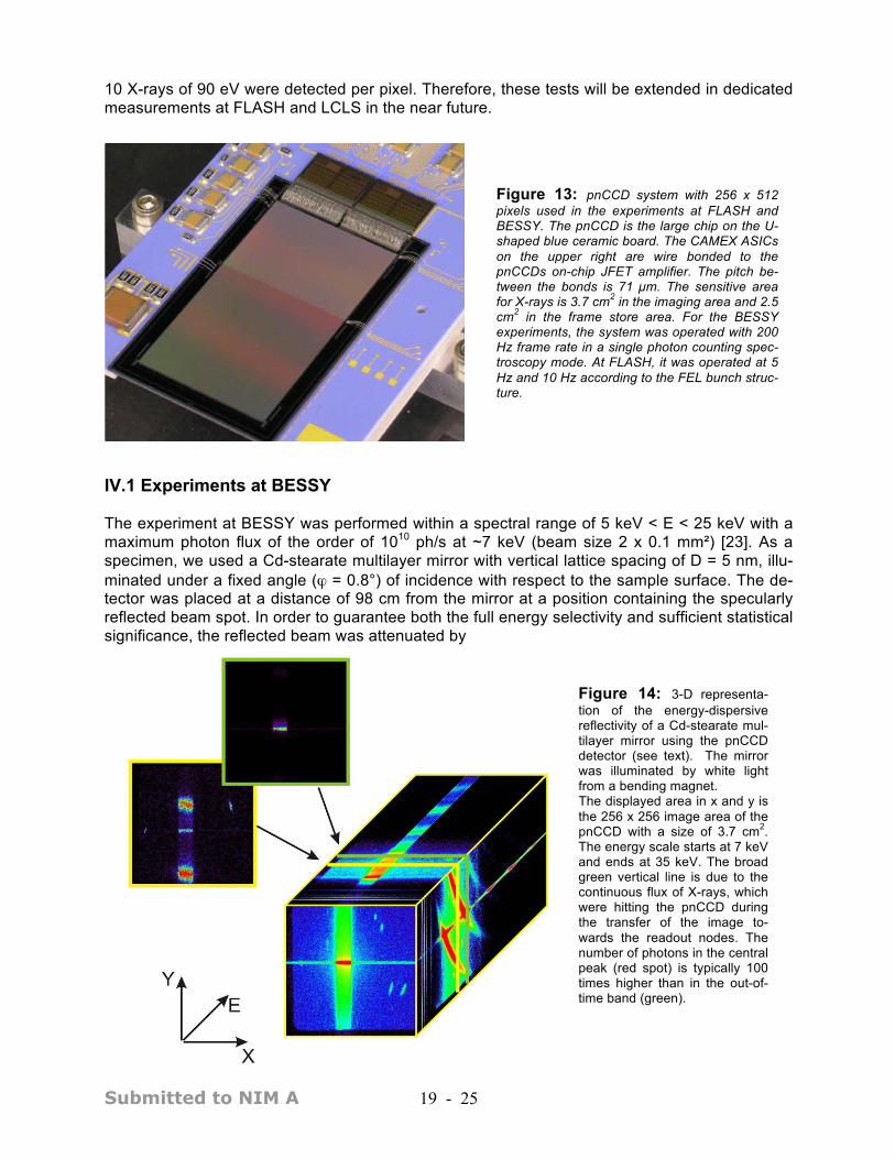
10 X-rays of 90 eV were detected per pixel. Therefore, these tests will be extended in dedicated measurements at FLASH and LCLS in the near future. IV.1 Experiments at BESSY The experiment at BESSY was performed within a spectral range of 5 keV < E < 25 keV with a maximum photon flux of the order of 1010 ph/s at ~7 keV (beam size 2 x 0.1 mm²) [23]. As a specimen, we used a Cd-stearate multilayer mirror with vertical lattice spacing of D = 5 nm, illu-minated under a fixed angle (ϕ = 0.8°) of incidence with respect to the sample surface. The de-tector was placed at a distance of 98 cm from the mirror at a position containing the specularly reflected beam spot. In order to guarantee both the full energy selectivity and sufficient statistical significance, the reflected beam was attenuated by
Figure 14: 3-D representa-tion of the energy-dispersive reflectivity of a Cd-stearate mul-tilayer mirror using the pnCCD detector (see text). The mirror was illuminated by white light from a bending magnet. The displayed area in x and y is the 256 x 256 image area of the pnCCD with a size of 3.7 cm2. The energy scale starts at 7 keV and ends at 35 keV. The broad green vertical line is due to the continuous flux of X-rays, which were hitting the pnCCD during the transfer of the image to-wards the readout nodes. The number of photons in the central peak (red spot) is typically 100 times higher than in the out-of-time band (green).
Figure 13: pnCCD system with 256 x 512 pixels used in the experiments at FLASH and BESSY. The pnCCD is the large chip on the U- shaped blue ceramic board. The CAMEX ASICs on the upper right are wire bonded to the pnCCDs on-chip JFET amplifier. The pitch be-tween the bonds is 71 µm. The sensitive area for X-rays is 3.7 cm2 in the imaging area and 2.5 cm2 in the frame store area. For the BESSY experiments, the system was operated with 200 Hz frame rate in a single photon counting spec-troscopy mode. At FLASH, it was operated at 5 Hz and 10 Hz according to the FEL bunch struc-ture.

Submitted to NIM A 20 - 25
10 15 20 25
10
100
1000
10000
Δqz = 0.115 Å-1 ( d = 27.32 Å )
qz in Å-1
0.30.20.1
In
tens
ity
Energy in keV
pn-CCD SDD
thin aluminum foils to an integrated intensity below 105 counts/s. The signal was continuously recorded for a few minutes with a read-out speed of 200 frames per second, corresponding to typical repetition rates at LCLS or SCSS. It was the aim of the experiment to simultaneously rec-ord position and energy of the incident X-rays. Therefore, we needed to make sure that any pixel on the pnCCD is hit only once during the 5 ms integration time of a single frame. After integra-tion of many frames, the data can be presented as 2D frames (X,Y spatial coordinates) repre-senting a plane perpendicular to the direction of the reflected beam stacked along a 3rd dimen-sion, i.e. the energy, E (see Fig. 14) [22]. In such a representation, each 2D frame corresponds to a single GISAXS (Grazing-Incidence Small-Angle X-ray Scattering) image as it is typically recorded in monochromatic experiments without energy dispersive detection. As can be seen clearly in the insets in Figure 14, which show the extension along the X and Y directions of the photons for different energies, the X-dimension is limited by the lateral beam size of 2 mm. The intensity band along Y contains the specularly reflected beam at the reflection angle and diffusely scattered intensity whenever αf fulfills the Bragg condition αf = 6.4/(2·D·E). αi denotes the incident angle, α f the outgoing angle with respect to the scattering plane. Additional spots seen in the front plane stem from Bragg reflection of the 2D lattice of the Cd ions. The planes (X,E) and (Y,E) show a series of Bragg peaks lined up along the E-axis at Y=0 or X=0, respectively. The Bragg peak intensity is extended along the direction oblique to the E-axis representing the diffuse-resonant scattering originating from the correlated interface rough-ness of the multilayer. In a conventional experiment using monochromatic radiation, the (X,E) 2D map is typically rec-orded by a series of consecutive scans of αf for fixed αi. Similarly, the (Y,E) map requires varia-tion of an angle perpendicular to the incident plane for fixed αf or αi. Obviously, any line scan can be extracted from the 3D data field when the 2D spatial images are taken as a function of the photon energy and using white incoming light. As an example, a line scan of specular reflectivity is presented in Fig. 15. It clearly shows two multilayer Bragg peaks and additional Kiessig fring-es with higher oscillation frequency, which provides a measure of the total thickness of the multi-layer film [8]. For comparison, we have also plotted a scan recorded by an energy-dispersive point detector (Röntec XFlash) under the same geometric conditions and which is denoted by the solid line (SDD) in the figure. The additional, upper scale in Fig. 15 represents the reciprocal
Figure 15: Energy line scan along the specular direction extracted from the 3-D data shown in Fig.15. Data from the pnCCD (filled circles) are compared to the results obtained with an en-ergy dispersive point detec-tor (line denoted by “SDD”; see text). The detector sys-tems were not cross cali-brated. For details see [22].

Submitted to NIM A 21 - 25
space coordinate qz corresponding to the real space coordinate E in the lower scale. Obviously, the results obtained by both detectors are very similar and only differ in the relative intensity at the higher photon energies. The data evaluation in terms of q-space and further experimental details have been published in [23]. In summary, the test measurements at the BESSY synchrotron clearly prove the single photon counting, energy dispersive capabilities of our detector that were recorded at a frame read-out speed matching the repetition rates at the LCLS and SCSS. Moreover, the present results im-pressively underline the advantage of using a pnCCD for such kind of experiments. In essence, the pnCCD combines 256 x 256 independent energy-dispersive point detectors which give a clear advantage for white-beam experiments if the energy resolution of the pnCCD is sufficient for the process under investigation. IV.2 Experiments at FLASH As mentioned in the introduction, intense, short-wavelength femtosecond light pulses from free electron lasers are expected to open the door to a wide variety of investigations with unprece-dented spatial and temporal resolution [24]. Along these lines, nano-sized clusters emerging from a supersonic jet were irradiated at FLASH with about 1012 photons per shot, focused to a spot size of a few microns, corresponding to power densities exceeding 1014 W/cm2. Under the-se conditions, the sample in the laser focus is completely ionized on a femtosecond time scale [25]. This initiates a whole series of secondary effects such as ultra-fast electron migration, Cou-lomb explosion [26] and plasma recombination [27], potentially accompanied by the emission of fluorescence radiation, which has yet to be observed. As outlined in the introduction, imaging of nanostructures [28] requires that their sub-nanometer order is not obscured or destroyed by the FEL beam within the timescale necessary for image detection. Gaining insight into the underly-ing ultra-short, non-linear dynamic processes in the short wavelength, intense laser regime through single shot photon scattering experiments is of utmost importance for reaching this goal.
Figure 16: Energy resolution measured at FLASH with 90 eV VUV photons. Every photon generates approximately 25 electron-hole pairs. They have been detected with a read noise of 2.5 electrons (rms). The measured FWHM is only 38.9 eV. The plot contains all events: signal pile-up as well as pattern pile-up and split events. Events hitting two neighbouring pixels have been recombined to one entry in the spectrum.
Submitted to NIM A 22 - 25
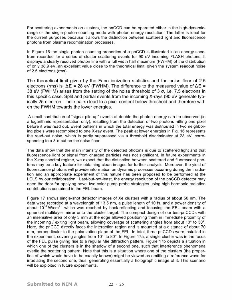
For scattering experiments on clusters, the pnCCD can be operated either in the high-dynamic-range or the single-photon-counting mode with photon energy resolution. The latter is ideal for the current purposes because it allows the distinction between scattered light and fluorescence photons from plasma recombination processes. In Figure 16 the single photon counting properties of a pnCCD is illustrated in an energy spec-trum recorded for a series of cluster scattering events for 90 eV incoming FLASH photons. It displays a clearly resolved photon line with a full width half maximum (FWHM) of the distribution of only 38.9 eV, an excellent value close to the theoretical limit, given the system readout noise of 2.5 electrons (rms). The theoretical limit given by the Fano ionization statistics and the noise floor of 2.5 electrons (rms) is ΔE = 28 eV (FWHM). The difference to the measured value of ΔE = 38 eV (FWHM) arises from the setting of the noise threshold of 3 σ, i.e. 7.5 electrons in this specific case. Split and partial events from the incoming X-rays (90 eV generate typ-ically 25 electron – hole pairs) lead to a pixel content below threshold and therefore wid-en the FWHM towards the lower energies. A small contribution of “signal pile-up” events at double the photon energy can be observed (in a logarithmic representation only), resulting from the detection of two photons hitting one pixel before it was read out. Event patterns in which the total energy was distributed in two neighbor-ing pixels were recombined to one X-ray event. The peak at lower energies in Fig. 16 represents the read-out noise, which is partly suppressed via a threshold discriminator at 28 eV, corre-sponding to a 3-σ cut on the noise floor. The data show that the main intensity of the detected photons is due to scattered light and that fluorescence light or signal from charged particles was not significant. In future experiments in the X-ray spectral regime, we expect that the distinction between scattered and fluorescent pho-tons may be a key feature for obtaining clean images for further analysis. Moreover, the yield of fluorescence photons will provide information on dynamic processes occurring during the irradia-tion and an appropriate experiment of this nature has been proposed to be performed at the LCLS by our collaboration. Last-but-not-least, the energy resolution of the pnCCD detector may open the door for applying novel two-color pump-probe strategies using high-harmonic radiation contributions contained in the FEL beam. Figure 17 shows single-shot detector images of Xe clusters with a radius of about 50 nm. The data were recorded at a wavelength of 13.5 nm, a pulse length of 10 fs, and a power density of about 1014 W/cm2 , which was reached by back-reflecting and focusing the FEL beam with a spherical multilayer mirror onto the cluster target. The compact design of our test-pnCCDs with an insensitive area of only 3 mm at the edge allowed positioning them in immediate proximity of the incoming / exiting light beam, allowing coverage of scattering angles from about 10° to 30°. Here, the pnCCD directly faces the interaction region and is mounted at a distance of about 70 mm, perpendicular to the polarization plane of the FEL. In total, three pnCCDs were installed in the experiment, covering angles from 10° to 80°. In Figure 17a, a single cluster was in the focus of the FEL pulse giving rise to a regular Mie diffraction pattern. Figure 17b depicts a situation in which one of the clusters is in the shadow of a second one, such that interference phenomena overlie the scattering pattern. Note that this is a situation where one of the clusters (the proper-ties of which would have to be exactly known) might be viewed as emitting a reference wave for irradiating the second one, thus, generating essentially a holographic image of it. This scenario will be exploited in future experiments.

Submitted to NIM A 23 - 25
Importantly, the present measurements indicate that even weakly bound van-der-Waals systems “stay intact” for the duration of the pulse insofar as the position of the atoms and their overall ex-tension is concerned. Detailed inspection of the intensity of the diffraction rings covering a larger area obtained when the three pnCCDs were in place, however, also clearly shows that the re-fractive index of the clusters has changed significantly during the pulse. This provides a first di-rect hint on the ultra-fast, few-femtosecond electron dynamics initiated by the FEL light. Since in any experiment with sub-nanometer resolution the short-wave length, keV energy FEL radiation is mainly absorbed by inner-shell electrons with cross sections exceeding those for elastic scat-tering by at least one order of magnitude at 10 keV, the ultra-fast rearrangement of the electrons might pose serious challenges. Indeed, present scenarios assume that the FEL pulse has to be shorter than 10 fs, the typical life time of a carbon K-shell hole against Auger-decay, in order to suppress effectively its decay setting free another electron from the L-shell. Under conditions that are assumed to be suited for “single-molecule imaging”, namely 1013 photons focused to a spot of 100 nm diameter, K-shell electrons are removed at an average rate of about one per 100 attoseconds. Thus, the second K-shell electron will be immediately removed as well, and, if the pulse is longer than the Auger life-time, the “refilled” K-shell electron is also removed, resulting in the delocalization of at least four electrons from each carbon atom within less than 10 fs (taking shake-off processes not into account). Our present results provide a first glimpse on such ultra-fast electronic response functions in nano-scaled, mesoscopic objects in terms of a modified refractive index that has to be used to explain the experimental data. In general, this impressively underlines the unique information that can be retrieved from single shot, energy and angular dispersive photon diffraction and fluo-rescence measurements, which will be indispensable to approach the final goal of single shot molecule imaging. The present data also clearly prove that the pnCCDs can be safely and relia-bly operated under typical FEL and single particle imaging conditions.
Figure 17: Single shot diffraction images of clusters taken with a pnCCD camera. a) a single cluster was hit by the FEL pulse. b) one cluster in the shadow of another one leads to a fine interference pattern in the scatter-ing signal. The FLASH photon energy was 91.9 eV (13.5 nm). The images are taken in the single photon per pixel counting limit, allowing spectral analysis of each pixel with the resolution shown in Fig. 17.

Submitted to NIM A 24 - 25
V. Conclusion We have planned, designed and assembled a novel multi-purpose, highly flexible end station, the CFEL-ASG Multi-Purpose (CAMP) chamber, for a large variety of applications at upcoming free electron lasers spanning the VUV to the hard X-ray wavelength regimes. The CAMP cham-ber accommodates a unique combination of various state-of-the-art imaging detector concepts. Two broad-range, energy dispersive (50 eV to 25 keV), single-photon-counting, and large area pnCCD pixel detector systems are flexibly mounted together with improved, high-resolution reac-tion microscope or velocity map imaging spectrometer devices for coincident multi-dimensional electron and ion momentum imaging. In its fully equipped operation mode, this allows, for the first time, simultaneous detection of angular- and energy- (momentum-resolved) electrons, ions, and scattered or fluorescent photons. From these correlated (in some cases, even coincident) and time-dependent many-particle data, we expect to obtain complete information on the dy-namic processes occurring when ultra-intense FEL pulses at X-ray photon energies interact with matter, with single atoms and ions, with simple to complex molecules, with clusters and other nano-particles, with solid matter, surfaces or plasmas - all of which are a completely unexplored terra incognita of light–matter interaction. Details of the chambers, the outline, design and mounting of the different targets and detectors, partly to be completed in subsequent phases, have been provided. Moreover, the results of ex-tensive tests of the pnCCDs obtained at the BESSY synchrotron as well as at FLASH have been presented and demonstrate their capabilities for future experiments at X-ray free electron laser sources. This system will be employed in the first round of experiments at the LCLS in Novem-ber 2009. VI. Acknowledgements Support by central funds of the Max-Planck Society for advancing the science with FEL sources within the Advanced Study Group at the CFEL and previous support within the “Innovation Fund” of the President is gratefully acknowledged. Production and testing of the pnCCD devices would have been impossible without the excellent work of the staff of MPI semiconductor laboratory, the help of the DESY staff during beamtimes. The project was partially supported by BMBF no 05KS7KT1 and 05KS7PSA and Virtuelles Institut grant VH-VI-302. MPI semiconductor laborato-ry acknowledges the support of the Johannes-Heidenhain-Stiftung. Funding from the European XFEL for the simulation studies of the charge spreading is gratefully acknowledged.

Submitted to NIM A 25 - 25
References [1] V. Ayvazyan et al., Eur. Phys. Lett 100 (2008) 133401; W. Ackermann et al., Nat. Photonics 1 (2007) 336 [2] LCLS Conceptual Design Report, SLAC-R-593, April 2002, UC-414 [3] T. Shintake et al., Nat. Photonics 2 (2008) 555 [4] M. Altarelli, et al., eds., European XFEL Technical Design Report (DESY 2006-097, Hamburg, Germany, 2006), ISBN 978-3-935702-17-1 [5] M. Porro et al., NSS conference record, IEEE 19-25 Oct. 2008 , Page(s): 1578-1586 [6] R. Moshammer et al., Nucl. Instr. Meth. B 108 (1996) 425 and J. Ullrich et al., Rep. Prog. Phys. 66 (2003) 223202 [7] A.T. Eppink and D.H. Parker, Rev. Sci. Instr. 68 (1997) 3477 [8] T. Geue et al., J. Chem. Phys. 110 (1999) 8104 [9] O. Jagutzki et al., IEEE Trans. Nucl. Sci. 49 (2002) 2477 [10] H. Fukuzawa et al., Phys. Rev. A 79 (2009) 031201 [11] M. Kurka et al., J. Phys. B: At. Mol. Opt. Phys. 42 (2009) 141002 [12] R. Moshammer et al., Phys. Rev. Lett. 98 (2007) 203001 [13] A. Rudenko et al., Phys. Rev. Lett. 101 (2008) 073003 [14] Y.H. Jiang et al., Phys. Rev. Lett. 102 (2009) 123002 [15] A. Vredenborg et al., Rev. Sci. Instr. 79 (2008) 063108 [16] P. Johnsson et al., J. Mod. Optics 55 (2008) 2693 [17] D. Rolles et al., Nucl. Instr. Meth. B 261 (2007) 170 [18] L. Strüder et al., Rev. Sci. Instr. 68 (1997) 4271 [19] L. Strüder et al., Astronomy & Astrophysics 365 (2001) 18 [20] L. Strüder et al., NIM A 288 (1990) 227 [21] S. Herrmann et al., NSS conf. record ’07 , Vol. 3, (2007) 2398 [22] H.J. Fitting, Phys. Stat. Sol. (a) 26 (1974) 525 [23] W. Leitenberger et al., J. Synchrotron. Rad. 15 (2008) 449 [24] C. Bostedt et al., NIM A 601 (2009), 108 [25] C. Bostedt et al., Phys. Rev. Letters, 100 (2008) 133401 [26] H. Thomas et al., J. Phys. B: At. Mol. Opt. Phys. 42 (2009) 134018 [27] M. Hoener et al., J. Phys. B: At. Mol. Opt. Phys. 41 (2008) 181001 [28] H. Chapman et al., Nature, 448 (2007) 676