large area detectors and new sensor technologies at ... · astronomical telescopes and...
TRANSCRIPT

Astronomical Telescopes and Instrumentation 24-31 May 2006, SPIE 6276-5
Large area detectors and new sensor Large area detectors and new sensor technologies at Fairchild Imaging technologies at Fairchild Imaging
Paul Vu, Chiao Liu, Dan Laxson

© Fairchild Imaging 2Astronomical Telescopes and Instrumentation
24-31 May 2006, SPIE 6276-5
OutlineOutline
• Introduction• Large area CCD detectors at Fairchild Imaging• MTF optimization of 4k x 4k CCD• CCD-CMOS hybrid technology status• Summary

© Fairchild Imaging 3Astronomical Telescopes and Instrumentation
24-31 May 2006, SPIE 6276-5
IntroductionIntroduction
• Fairchild Imaging manufactures advanced image sensors for industrial, scientific, and medical applications
• Full line of wafer-scale sensors• Monolithic sensors 8 x 8 cm2
• Pixel size 8.75 µm to 40 µm• High speed low noise CMOS• In-house CCD wafer fab• Large format back-illuminated
CCDs in high volume
Fairchild Imaging sensor manufacturing facilities are located in Milpitas, California

© Fairchild Imaging 4Astronomical Telescopes and Instrumentation
24-31 May 2006, SPIE 6276-5
OutlineOutline
• Introduction• Large area CCD detectors at Fairchild Imaging• MTF optimization of 4k x 4k CCD• CCD-CMOS hybrid technology status• Summary

© Fairchild Imaging 5Astronomical Telescopes and Instrumentation
24-31 May 2006, SPIE 6276-5
Large area CCD detectorsLarge area CCD detectors
CCD part number
Format H x V (pixels)
Pixel size (µm2)
Imaging area (H x V, mm) Features
CCD485 4k x 4k 15 x 15 61.20 x 61.21 Frontside, 3-phase, MPP, 4 outputs
CCD486 4k x 4k 15 x 15 61.44 x 61.45 Front or back-illuminated, 4 outputs
CCD595 9k x 9k 8.75 x 8.75 80.64 x 80.64 Frontside, eight 25-MHz outputs
CCD8161 4k x 4k 19.5 x 19.5 79.87 x 79.87 Frontside, 3-side butting, 4 low-noise and 4 high-speed outputs
CCD3041 2k 2k 15 x 15 30.72 x 30.72 Front or back-illuminated, 4 outputs

© Fairchild Imaging 6Astronomical Telescopes and Instrumentation
24-31 May 2006, SPIE 6276-5
Monolithic 9k x 9k CCD595Monolithic 9k x 9k CCD595
• Developed for aerial reconnaissance• 9216(H) x 9216(V) full frame CCD• 8.75 µm x 8.75 µm pixels• 80.64 x 80.64 mm image area• 100% fill factor• 3-phase parallel shift registers• 2-phase serial shift registers• Buried channel CCD• 8 high-speed output amplifiers
• Readout noise <30 e- at 25 MHz• 200 MHz data rate (25 MHz x 8)• Flight package with TEC coolers
CCD595 in ceramic package

© Fairchild Imaging 7Astronomical Telescopes and Instrumentation
24-31 May 2006, SPIE 6276-5
4k x 4k CCD81614k x 4k CCD8161
• Developed for mosaic applications• 3-side abuttable• 4096(H) x 4096(V) full frame CCD• 19.5 µm x 19.5 µm pixels• 79.87 mm x 79.87 mm active area• 100% fill factor• Front and back-illuminated• Multi-Pinned Phase (MPP)• 8 selectable output ports
– 4 low-noise– 4 high-speed
• 3-phase vertical and serial registers• Supports pixel binning
© Fairchild Imaging 8Astronomical Telescopes and Instrumentation
24-31 May 2006, SPIE 6276-5
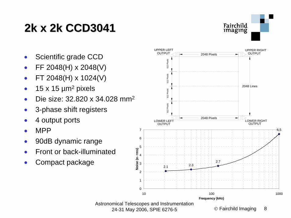
2k x 2k CCD30412k x 2k CCD3041UPPER RIGHT
LOWER RIGHT
OUTPUT
OUTPUT
2048 Pixels
2048 Pixels
512
Pixe
ls51
2 P
ixel
s51
2 P
ixel
s51
2 P
ixel
s
2048 Lines
LOWER LEFTOUTPUT
UPPER LEFTOUTPUT
6.5
2.72.32.1
0
1
2
3
4
5
6
7
10 100 1000Frequency (kHz)
Noi
se (e
- rm
s)
• Scientific grade CCD• FF 2048(H) x 2048(V)• FT 2048(H) x 1024(V)• 15 x 15 µm2 pixels• Die size: 32.820 x 34.028 mm2
• 3-phase shift registers• 4 output ports• MPP• 90dB dynamic range• Front or back-illuminated• Compact package

© Fairchild Imaging 9Astronomical Telescopes and Instrumentation
24-31 May 2006, SPIE 6276-5
OutlineOutline
• Introduction• Large area CCD detectors at Fairchild Imaging• MTF optimization of 4k x 4k CCD• CCD-CMOS hybrid technology status• Summary

© Fairchild Imaging 10Astronomical Telescopes and Instrumentation
24-31 May 2006, SPIE 6276-5
4k x 4k CCD4864k x 4k CCD486
Back-illuminated CCD486
Front-illuminated CCD486
• 4096(H) x 4097(V) full frame CCD• 15 µm x 15 µm pixels• 61.44 mm x 61.44 mm image area• 100% fill factor• Front and back-illuminated• Multi-Pinned Phase (MPP) mode• Readout noise < 3 e- at 50 kHz• Full well > 100 ke-
• 4 output ports• 3-phase buried channel CCD• Supports pixel binning• Notch channels for improved
radiation tolerance

© Fairchild Imaging 11Astronomical Telescopes and Instrumentation
24-31 May 2006, SPIE 6276-5
CCD486 performanceCCD486 performance
0
1
2
3
4
5
6
7
8
9
10
100 1000Frequency (kHz)
Rea
d no
ise
(e- r
ms)
Overscan
Image
Parameter Typical measured value Units Vertical full well (1 x 1) 102,000 e- Horizontal full well 760,000 e- Par. & Hor. CTE at 1000 e- 0.999998 Par. & Hor. CTE at 60,000 e- 0.999999 Read noise at 250 kHz < 4 e- Read noise at 1 MHz < 7 e- Dark current at -60°C 0.02 e-/pix/sec PRNU, measured at half sat 5 % full well DSNU at +30°C 25 pA/cm2 p-p Non-linearity (up to 80% FW) < 1 %

© Fairchild Imaging 12Astronomical Telescopes and Instrumentation
24-31 May 2006, SPIE 6276-5
Backside thinning processBackside thinning process
• Known-good CCD is bonded to substrate
• Special mask is applied to define thinned area
• Selective chemical etch removes bulk Si
• Perform back surface accumulation process and AR coating
• Mount die in package and wirebond
• Stable and well controlled CCD thinning process performed in high volume
P+
P-
Support Substrate
CCD die
Underfillepoxy
P-
Support Substrate
HF : HNO3 : CH3COOH
1. Bond die to substrate,protect non-active areas
2. Selective chemical etch
P-
Support Substrate
3. Back surface processing and AR coating4. Die attach and wirebond

© Fairchild Imaging 13Astronomical Telescopes and Instrumentation
24-31 May 2006, SPIE 6276-5
Diffusion MTF effectsDiffusion MTF effects
• Carrier diffusion in the field free region degrades the MTF
• Field free region is effectively eliminated by sufficiently large bias on high resistivity material
• Fully depleted CCD concept
• Fully depleted CCD offers excellent MTF characteristics, but add process complexity and increase in dark current
• The field free region can be minimized by additional thinning
Depletion layer
Undepleted neutral layer
e-
e-
e-e-
LW SW
Potential well
hν
SiO2 p-Si frontsidegate
e-
n-buriedchannel
field-freeregion
e-
depletion width ∝ SiR
depletion region
Front-Illuminated Back-Illuminated

© Fairchild Imaging 14Astronomical Telescopes and Instrumentation
24-31 May 2006, SPIE 6276-5
CCD486 MTF optimizationCCD486 MTF optimization
• Silicon thinned to ~ 10 µm compared to standard ~ 20 µm • MTF at Nyquist frequency improved ~3x at 410 nm
© Fairchild Imaging 15Astronomical Telescopes and Instrumentation
24-31 May 2006, SPIE 6276-5
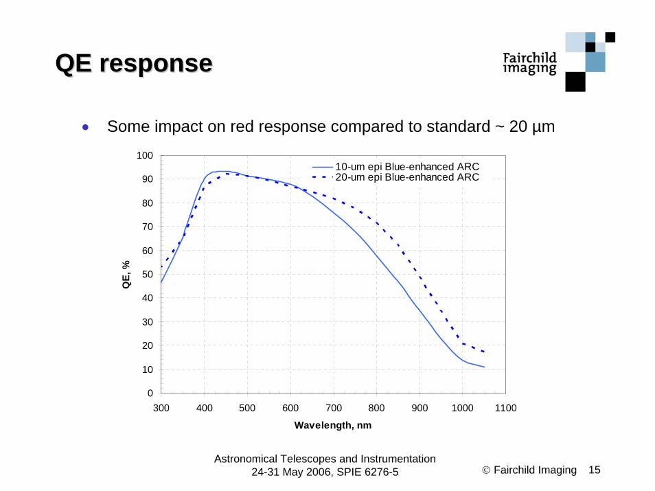
QE responseQE response
• Some impact on red response compared to standard ~ 20 µm
0
10
20
30
40
50
60
70
80
90
100
300 400 500 600 700 800 900 1000 1100
Wavelength, nm
QE,
%
10-um epi Blue-enhanced ARC20-um epi Blue-enhanced ARC

© Fairchild Imaging 16Astronomical Telescopes and Instrumentation
24-31 May 2006, SPIE 6276-5
OutlineOutline
• Introduction• Large area CCD detectors at Fairchild Imaging• MTF optimization of 4k x 4k CCD• CCD-CMOS hybrid technology status• Summary
© Fairchild Imaging 17Astronomical Telescopes and Instrumentation
24-31 May 2006, SPIE 6276-5
MotivationsMotivations
• Many scientific, medical, and military imaging applications require optical quality, high speed and low noise performance that exceed standard CCD or CMOS image sensor technology– Wavefront sensing for Adaptive Optics– Synchrotron x-ray crystallography– Night vision surveillance
• Requirements– Photon counting sensitivity – Resolution: 1M ~ 100M pixels – Frame rate: 30 Hz ~ 3 kHz– Minimal or no cooling– Low power

© Fairchild Imaging 18Astronomical Telescopes and Instrumentation
24-31 May 2006, SPIE 6276-5
Existing technologiesExisting technologies
• Monolithic CMOS image sensor– Low power, and system integration capability– High dark current, low QE, high read noise
• Conventional scientific CCD– Near ideal imaging performance — high QE, low dark
current, excellent uniformity– Elevated noise at high frame rates
• EMCCD– Very low-noise performance– Not suitable for some applications due to cooling and power
requirements

© Fairchild Imaging 19Astronomical Telescopes and Instrumentation
24-31 May 2006, SPIE 6276-5
Benefits of hybrid architectureBenefits of hybrid architecture
• Highly parallel architecture– Enables high frame rates at low noise– Eliminates high-power, high-bandwidth, on-chip CCD amplifiers– Uses low-bandwidth low-noise, high gain amplifiers in CMOS ROIC
• Low noise CMOS ROIC design– High conversion gain via LFPN CTIA– Bandwidth limiting for low noise– Low-power and high-speed performance
• Optimized CCD performance– Low dark current with MPP or pinned photodiode technology– Flexible CCD architecture: frame transfer (FT), interline transfer
(IT), front or back-illuminated– Charge binning capability for improved SNR

© Fairchild Imaging 20Astronomical Telescopes and Instrumentation
24-31 May 2006, SPIE 6276-5
CCDCCD--CMOS hybrid architectureCMOS hybrid architecture
CCD Clock Drivers
Control
Digital Output
Indium Bump Bonding
Shielded Storage Area
CMOS CIRCUIT
Shielded Storage Area
CMOS CIRCUIT
CCD Clock Drivers
Control
Digital Output
1280 Columns
1024
Row
sCharge Coupled Device
• CMOS ROICs directly coupled to CCD• CCD contains no output amplifiers• Charge to voltage conversion performed in CMOS ROIC

© Fairchild Imaging 21Astronomical Telescopes and Instrumentation
24-31 May 2006, SPIE 6276-5
Frame transfer CCDFrame transfer CCD
Shielded Storage Area
Shielded Storage Area
Sense node
V1
V4
V3
V2
V1
Channel stops
CCD channel

© Fairchild Imaging 22Astronomical Telescopes and Instrumentation
24-31 May 2006, SPIE 6276-5
Interline frame transfer CCDInterline frame transfer CCD
Shielded Storage Area
Shielded Storage Area
Photodiode
Shielded vertical registers
Sense node
1
1
3
3 4
2
2
Shielded vertical registers
Shielded vertical registers
© Fairchild Imaging 23Astronomical Telescopes and Instrumentation
24-31 May 2006, SPIE 6276-5
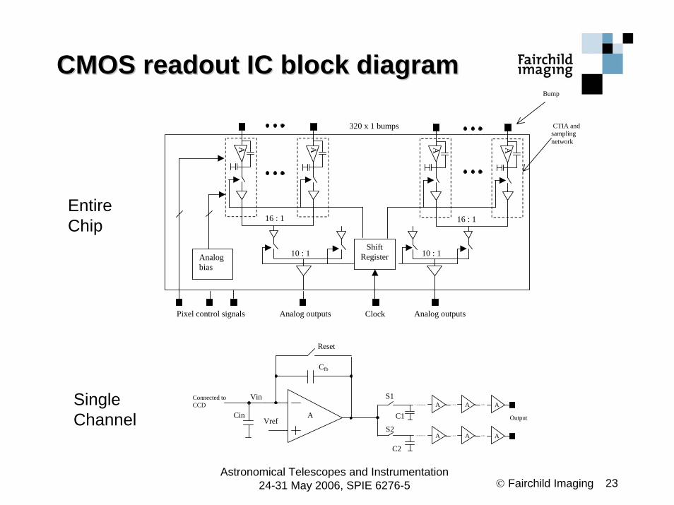
CMOS readout IC block diagramCMOS readout IC block diagram
S1
C1
S2
C2
Vref
Reset
Cfb
Cin A
VinConnected toCCD
A A A
A A A
Output
CTIA andsamplingnetworkA A A A
16 : 1 16 : 1
320 x 1 bumps
ShiftRegister
Pixel control signals Analog outputs
Bump
Analogbias
Clock
10 : 1 10 : 1
Analog outputs
Entire Chip
Single Channel

© Fairchild Imaging 24Astronomical Telescopes and Instrumentation
24-31 May 2006, SPIE 6276-5
Noise analysisNoise analysis
• CTIA is dominant noise source• The input referred noise power
spectral density includes thermal noise and 1/f
• Assuming that 1/f noise is removed by CDS, noise in e-rms is given by
Vn~
Cin
Cfb
Cload
AVout
fAmf
mn f
gKgkTfV
22
38)( +=
223
8in
m
CNBWqg
kTN ⋅⋅≈
AmplifierBWNBW2π
=where

© Fairchild Imaging 25Astronomical Telescopes and Instrumentation
24-31 May 2006, SPIE 6276-5
Estimated noise performanceEstimated noise performance
Noise as a function of frame rate

© Fairchild Imaging 26Astronomical Telescopes and Instrumentation
24-31 May 2006, SPIE 6276-5
Hybrid development statusHybrid development status
• Prototype 1280(H) x 1024(V) hybrid sensor demonstrated
• Frame transfer CCD• CMOS CTIA readout ICs• Read noise ~ 2.9 e- at 30 Hz
H1011 Characteristics
Format 1280(H) x 1024(V)Pixel size 12 x 12 µm2
Spectral range 400 - 1100 nmPeak QE 40%Conversion gain 160 uV/e-Non-linearity <1%Dynamic range high gain mode = 2000:1
low gain mode = 6000:1Dark current at 23 °C 6 - 8 pA/cm2
Smear at full saturation 0.05%Outputs 4 (multiplexed)Frame rate 1x1 unbinned 30 fps 2x2 binned 52 fps 4x4 binned 128 fps

© Fairchild Imaging 27Astronomical Telescopes and Instrumentation
24-31 May 2006, SPIE 6276-5
OutlineOutline
• Introduction• Large area CCD detectors at Fairchild Imaging• MTF optimization of 4k x 4k CCD• CCD-CMOS hybrid technology status• Summary

© Fairchild Imaging 28Astronomical Telescopes and Instrumentation
24-31 May 2006, SPIE 6276-5
SummarySummary
• Fairchild Imaging offers a unique family of scientific CCDs with ultra large imaging areas
• Reliable manufacturing capability• Improved MTF of back-illuminated 4K x 4K CCD• New breed of advanced sensors developed to
address the need for high speed and low noise performance