langmuir schaefer deposition of quantum dot multilayers
TRANSCRIPT

7732 DOI: 10.1021/la904474h Langmuir 2010, 26(11), 7732–7736Published on Web 02/03/2010
pubs.acs.org/Langmuir
© 2010 American Chemical Society
Langmuir-Schaefer Deposition of Quantum Dot Multilayers
Karel Lambert,† Richard K. �Capek,† Maryna I. Bodnarchuk,§, ) Maksym V. Kovalenko,§, )
Dries Van Thourhout,‡ Wolfgang Heiss,§ and Zeger Hens*,†
†Physics and Chemistry of Nanostructures, Ghent University, Krijgslaan 281-S3, 9000 Gent, Belgium,‡Department of Information Technology, Ghent University-IMEC, Sint-Pietersnieuwstraat 41, 9000 Gent,
Belgium, and §Institute of Semiconductor and Solid State Physics, University Linz, Altenbergerstrasse 69, 4040Linz, Austria. )Present address: Department of Chemistry, University of Chicago, Chicago, IL 60637.
Received November 26, 2009. Revised Manuscript Received January 14, 2010
The application of colloidal nanocrystals in various devices requires their assembly into well-defined mono- ormultilayers.We explore the possibilities of the Langmuir-Schaefer technique tomake such layers, using CdSe quantumdots as a model system. The layer quality is assessed using atomic force microscopy, transmission electron microscopy,andUV-vis absorption spectroscopy. For hydrophobic substrates, we find that the Langmuir-Schaefer technique is anexcellent tool for controlled multilayer production. With hydrophilic substrates, dewetting induces a cellular super-structure. Combination with photolithography leads to micropatterned multilayers, and combination of differentnanocrystal sizes allows for the formation of 2D binary superstructures.
1. Introduction
In the past 25 years, substantial progress has been made in thedevelopment of colloidal nanocrystal (NC) or quantum dot (QD)synthesis, leading to a controllable size, composition, shape, andsurface chemistry.1-3 Application of the unique QD properties indevices often requires the assembly of QDs. Single QD mono-layers have been used in the design of light-emitting diodes(LEDs),4 whereas QD multilayers are used for multicoloredlight-emitting films,5 biosensors,6 light-harvesting devices,7-9
photodetectors,10 F€orster resonant energy transfer (FRET) sen-sing,11,12 and LEDs.13 A good control over the layer quality isessential for the efficiency of these devices,4,13 and differentapproaches to achieve this have been reported.14 For example,well-definedmono- ormultilayers canbemadeusing conventional
layer-by-layer (LbL) assembly with15 or without11 polymer linkeror by spin-assisted LbL assembly,16,17 but all require water-soluble particles. For hydrophobic particles, an effective methodto produce ordered QD monolayers is their self-assembly at theair-water interface, followed by either vertical deposition(Langmuir-Blodgett technique18) or horizontal deposition(Langmuir-Schaefer technique19) on a substrate. The Langmuir-Schaefer (LS) and Langmuir-Blodgett (LB) techniques provideimportant advantages over other solution-phase processing tech-niques such as drying-mediated assembly20 and spin-coating,4 asthey allow deposition of closely packed QD layers of large areas,even on nonflat substrates.21 Moreover, the resulting layers can becombined with LbL assembly,22 used for subsequent microcontactprinting,19,23 ormicropatterning through combinationwith photo-lithography.21
Despite the importance of the technique, little attention hasbeen paid to the structure ofQDLSmultilayers. UsingCdSeQDs(Q-CdSe) as a model system, we deposit mono- and multilayerson glass and silicon and assess the layer quality using atomic forcemicroscopy (AFM),UV-vis absorption spectroscopy, and trans-mission electron microscopy (TEM). We find that the resultinglayer structure is influenced by the substrate hydrophobicity:either smooth layers or cellular networks can be obtained.Smooth multilayers contain various stacking sequences and canbe combined with optical lithography to create micropatternedmultilayers. Finally, by combination of Q-CdSe with Fe3O4
24
nanocrystals, we show how the LS technique enables the forma-tion of 2D binary QD superlattices.
*Corresponding author. E-mail: [email protected].(1) Murray, C. B.; Kagan, C. R.; Bawendi, M. G. Annu. Rev. Mater. Sci. 2000,
30, 545–610.(2) Yin, Y.; Alivisatosn, P. Nature 2005, 437, 664–670.(3) deMello Doneg�a, C.; Liljeroth, P.; Vanmaekelbergh, D. Small 2005, 1, 1152–
1162.(4) Coe, S.; Woo, W.; Bawendi, M.; Bulovic, V. Nature 2002, 420, 800–803.(5) Lin, Y.; Tseng, W.; Chang, H. Adv. Mater. 2006, 18, 1381–1386.(6) Li, X.; Zhou, Y.; Zheng, Z.; Yue, X.; Dai, Z.; Liu, S.; Tang, Z. Langmuir
2009, 25, 6580–6586.(7) Crooker, S. A.; Hollingsworth, J. A.; Tretiak, S.; Klimov, V. I. Phys. Rev.
Lett. 2002, 89, 186802.(8) Rogach, A. L.; Klar, T. A.; Lupton, J. M.; Meijerink, A.; Feldmann, J.
J. Mater. Chem. 2009, 19, 1208–1221.(9) Acherman, M.; Petruska, M. A.; Crooker, S. A.; Klimov, V. I. J. Phys.
Chem. B 2003, 107, 13782–13787.(10) Konstantatos, G.; Clifford, J.; Levina, L.; Sargent, E. H. Nat. Photonics
2007, 1, 531–534.(11) Franzl, T.; Shavel, A.; Rogach, A. L.; Gaponik, N.; Klar, T. A. Small 2005,
1, 392–395.(12) Gole, A.; Jana, N. R.; Selvan, S. T.; Ying, J. Y. Langmuir 2008, 24, 8181–
8186.(13) Bae, W. K.; Kwak, J.; Park, J. W.; Char, K.; Lee, C.; Lee, S. Adv. Mater.
2009, 21, 1690–1694.(14) Kinge, S.; Crego-Calama, M.; Reinhoudt, D. N. ChemPhysChem 2008, 9,
20–42.(15) Srivastava, S.; Kotov, N. A. Acc. Chem. Res. 2008, 41, 1831–1841.(16) Jiang, C.; Markutsya, S.; Pikus, Y.; Tsukruk, V. V. Nat. Mater. 2004, 3,
721–728.(17) Zimnitsky, D.; Jiang, C.; Xu, J.; Lin, Z.; Tsukruk, V. V. Langmuir 2007, 23,
4509–4515.
(18) Kotov, N. A.; Meldrum, F. C.; Wu, C.; Fendler, J. H. J. Phys. Chem. 1994,98, 2735–2738.
(19) Santhanam, V.; Andres, R. P. Nano Lett. 2004, 4, 41–44.(20) Lin, X.M.; Jaeger, H.M.; Sorensen, C.M.; Klabunde, K. J. J. Phys. Chem.
B 2001, 105, 3353–3357.(21) Lambert, K.; Moreels, I.; Van Thourhout, D.; Hens, Z. Langmuir 2008, 24,
5961–5966.(22) Lowman, G. M.; Nelson, S. L.; Graves, S. M.; Strouse, G. F.; Buratto, S.
Langmuir 2004, 20, 2057–2059.(23) Guo, Q.; Teng, X.; Rahman, S.; Yang, H. J. Am.Chem. Soc. 2003, 125, 630–
631.(24) Kovalenko, M. V.; Bodnarchuk, M. I.; Lechner, R. T.; Hesser, G.;
Sch€affler, F.; Heiss, W. J. Am. Chem. Soc. 2007, 129, 6352–6353.
DOI: 10.1021/la904474h 7733Langmuir 2010, 26(11), 7732–7736
Lambert et al. Article
2. Experimental Section
2.1. Nanocrystal Synthesis. Q-CdSe particles with a meandiameter of 3.1 and 3.4 nm were prepared based on the synthesisreported by Mulvaney and co-workers.25 A selenium (Se,99.999% Alfa Aesar) stock solution was made by heating amixture of Se powder (0.1263 g, 1.6 mmol) in n-octadecene(ODE, 16 mL, 90% Alfa Aesar) under a nitrogen atmosphere at195 �C for 2 h (until themixture became orange-yellow). Then themixture was cooled to room temperature, resulting in a transpar-ent yellow solution which was stable for weeks. For the nano-crystal synthesis, cadmium oxide (CdO, 0.36 mmol, 99.999%Strem), oleic acid (OA, 3.6mmol, 90%Sigma-Aldrich), andODE(12mL)weremixed anddegassed for 1 h at 100 �Cunder nitrogen,followed by heating to 250 �C until all CdO dissolved. Then thesolution was heated to 265 �C, and the Se stock solution (3.6 mL)was injected. The temperature of the mixture dropped afterinjection and the reaction continued at 235 �C for 4 min(diameter 3.1 nm, band gap absorption 544 nm) or 10 min(diameter 3.4 nm, band gap absorption 563 nm). After reaction,equal volumes of toluene and isopropanol were added, and theparticles were precipitated by adding methanol. Afterward, theparticles were further purified twice by resuspension in tolueneand precipitation with methanol. Synthesis of Fe3O4 nanoparti-cles is reported elsewhere.24
2.2. Layer Deposition. Q-CdSe and Fe3O4 monolayers wereproducedwith aNima312Dtrough.Typically, 30-50μLofaQDsuspension in toluene was spread dropwise on a water surface(250 cm2). Deinonized water with a resistivity above 5 � 104 Ωm-1 was used. The floating film was compressed at a rate of10 cm2 min-1 until a pressure of 12 mN m-1 was reached. Theresulting layer was transferred to the substrate by gently stampingthe substrate on the water surface containing the particles. Assubstrates we used glass microscopy slides and polished siliconcleaned with water and acetone. To obtain hydrophobic silicon,the native oxide of the silicon substrates was removed beforedeposition by etching with a 5% HF solution in water.
2.3. Characterization. The quality of the substrates anddeposited layers was assessed with a variety of characterizationmethods at different stages during the process. AFManalysis wasdone with a Molecular Imaging PicoPlus system in ac AFMmode. TEM samples were prepared by holding a carbon-coatedcopper grid between a pair of tweezers and briefly letting the gridtouch the nanocrystal film on thewater surface. The samples wereexamined using a Jeol 2200 FS microscope. UV-vis spectra ofnanocrystal suspensions and thin films were taken with a Perkin-Elmer Lambda 950 spectrophotometer.
2.4. Micropatterning. Local LS layer deposition was doneby LS deposition on silicon substrates covered with patternedphotoresist21 with a thickness of 300 nm. Subsequent resistdissolution is done by dipping the sample in acetone (45 s),isopropanol (30 s), and distilled water (15 s).
3. Results and Discussion
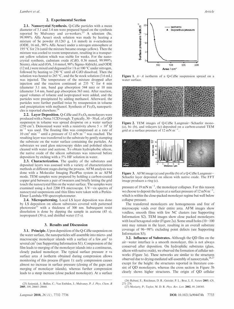
3.1. Principle.Upondeposition of theQ-CdSe suspensiononthe water surface, the nanoparticles self-assemble into micro- andmacroscopic monolayer islands with a surface of a few μm2 toseveral cm2 (see Supporting Information S1). Compression of thefilm leads to merging of the monolayer islands into a continuous,closely packed monolayer. The typical surface pressure π vssurface area A isotherm obtained during compression allowsmonitoring of this process (Figure 1): early compression causesalmost no increase in surface pressure (closing of the gaps andmerging of monolayer islands), whereas further compressionleads to a steep increase (close packed monolayer). At a surface
pressure of 19 mNm-1, the monolayer collapses. For this reasonwe choose to deposit the layers at a surface pressure of 12mNm-1,which is within the close-packedmonolayer regime but well belowcollapse pressure.
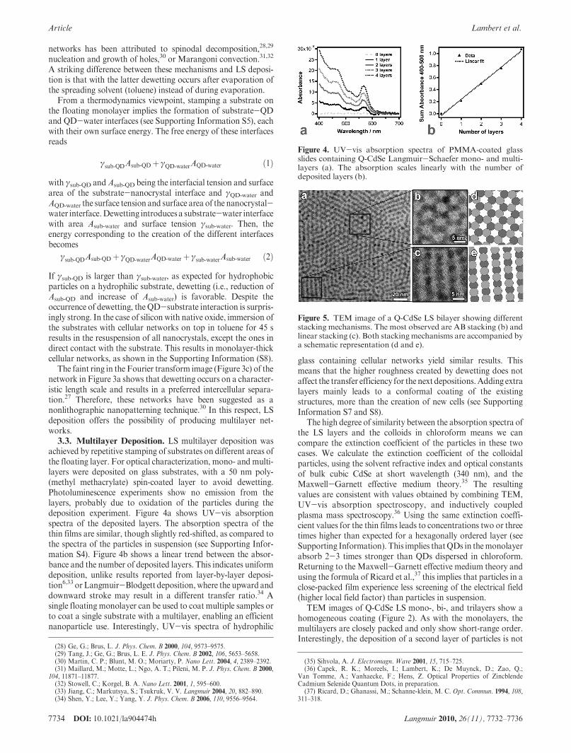
The transferred monolayers are homogeneous and free ofmicroscopic voids over their entire area. AFM images showvoidless, smooth films with few NC clusters (see SupportingInformation S2). TEM images show close packed monolayerswith local hexagonal order (Figure 2a). Some small holes (10-100nm) may remain in the layer, resulting in an overall substratecoverage of 96-98% excluding point defects (see SupportingInformation S3).3.2. Influence of Substrates. Although the QD film on the
air-water interface is a smooth monolayer, this is not alwaysconserved after deposition. On hydrophilic substrates (glass,siliconwith native oxide), we observed the formation of cellular net-works (Figure 3a). These networks are similar to the structuresobserved due to drying-mediated self-assembly of nanocrystals,26,27
except for the height: the structures reported in literature con-sist of QD monolayers, whereas the cross section in Figure 3bclearly shows higher structures. The origin of QD cellular
Figure 1. π-A isotherm of a Q-CdSe suspension spread on awater surface.
Figure 3. AFM image (a) and profile (b) of a Q-CdSe Langmuir-Schaefer layer deposited on silicon with native oxide. The FFTimage produces a ring (c).
Figure 2. TEM images of Q-CdSe Langmuir-Schaefer mono-(a), bi- (b), and trilayers (c) deposited on a carbon-coated TEMgrid at a surface pressure of 12 mNm-1.
(25) Jasieniak, J.; Bullen, C.; Van Embden, J.; Mulvaney, P. J. Phys. Chem. B2005, 109, 20665–20668.
(26) Rabani, E.; Reichman, D. R.; Geissler, P. L.; Brus, L. E. Nature 2003, 426,271–274.
(27) Moriarty, P.; Taylor, M. D. R. Phys. Rev. Lett. 2002, 89, 248303.
7734 DOI: 10.1021/la904474h Langmuir 2010, 26(11), 7732–7736
Article Lambert et al.
networks has been attributed to spinodal decomposition,28,29
nucleation and growth of holes,30 or Marangoni convection.31,32
A striking difference between these mechanisms and LS deposi-tion is that with the latter dewetting occurs after evaporation ofthe spreading solvent (toluene) instead of during evaporation.
From a thermodynamics viewpoint, stamping a substrate onthe floating monolayer implies the formation of substrate-QDand QD-water interfaces (see Supporting Information S5), eachwith their own surface energy. The free energy of these interfacesreads
γsub-QDAsub-QDþγQD-waterAQD-water ð1Þ
with γsub-QD andAsub-QD being the interfacial tension and surfacearea of the substrate-nanocrystal interface and γQD-water andAQD-water the surface tension and surface area of the nanocrystal-water interface.Dewetting introduces a substrate-water interfacewith area Asub-water and surface tension γsub-water. Then, theenergy corresponding to the creation of the different interfacesbecomes
γsub-QDAsub-QDþγQD-waterAQD-water þγsub-waterAsub-water ð2Þ
If γsub-QD is larger than γsub-water, as expected for hydrophobicparticles on a hydrophilic substrate, dewetting (i.e., reduction ofAsub-QD and increase of Asub-water) is favorable. Despite theoccurrence of dewetting, the QD-substrate interaction is surpris-ingly strong. In the case of silicon with native oxide, immersion ofthe substrates with cellular networks on top in toluene for 45 sresults in the resuspension of all nanocrystals, except the ones indirect contact with the substrate. This results in monolayer-thickcellular networks, as shown in the Supporting Information (S8).
The faint ring in the Fourier transform image (Figure 3c) of thenetwork in Figure 3a shows that dewetting occurs on a character-istic length scale and results in a preferred intercellular separa-tion.27 Therefore, these networks have been suggested as anonlithographic nanopatterning technique.30 In this respect, LSdeposition offers the possibility of producing multilayer net-works.3.3. Multilayer Deposition. LS multilayer deposition was
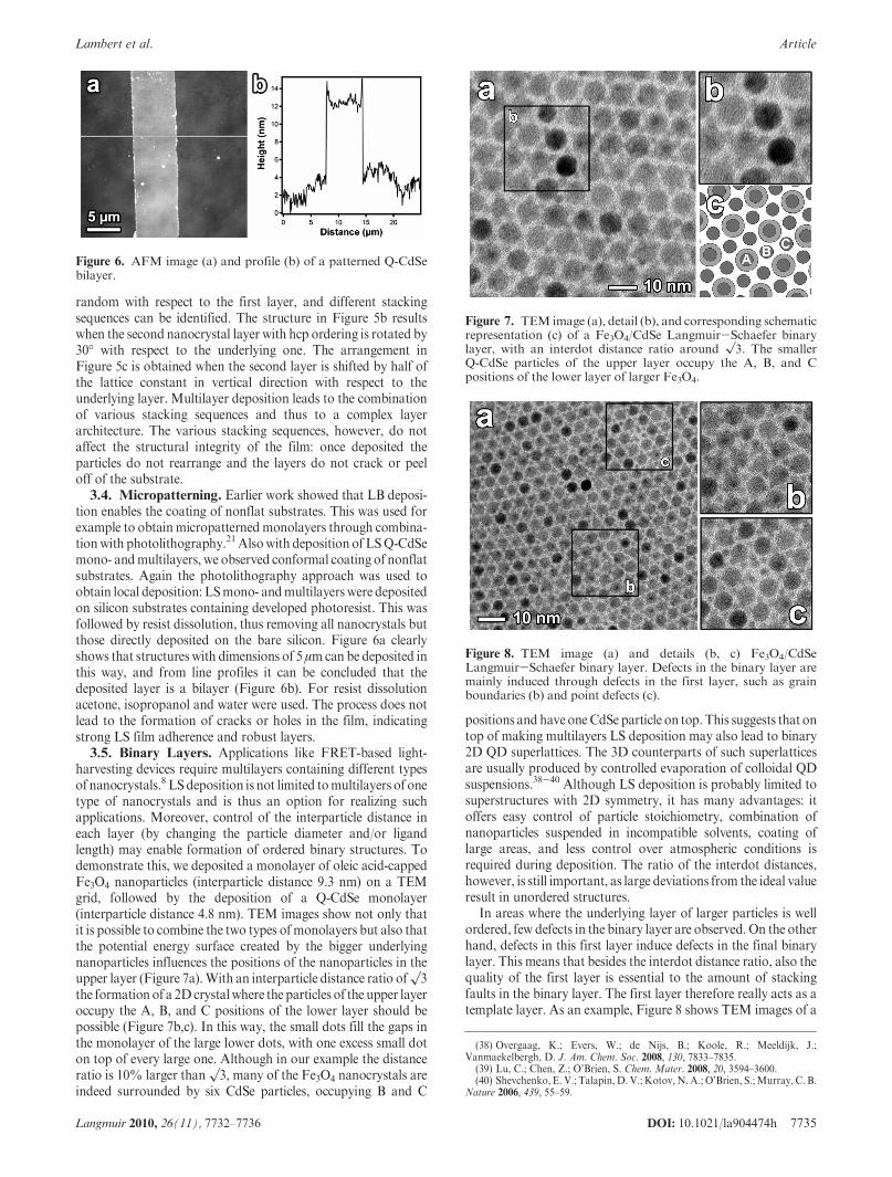
achieved by repetitive stamping of substrates on different areas ofthe floating layer. For optical characterization, mono- and multi-layers were deposited on glass substrates, with a 50 nm poly-(methyl methacrylate) spin-coated layer to avoid dewetting.Photoluminescence experiments show no emission from thelayers, probably due to oxidation of the particles during thedeposition experiment. Figure 4a shows UV-vis absorptionspectra of the deposited layers. The absorption spectra of thethin films are similar, though slightly red-shifted, as compared tothe spectra of the particles in suspension (see Supporting Infor-mation S4). Figure 4b shows a linear trend between the absor-bance and the number of deposited layers. This indicates uniformdeposition, unlike results reported from layer-by-layer deposi-tion6,33 orLangmuir-Blodgett deposition,where the upward anddownward stroke may result in a different transfer ratio.34 Asingle floating monolayer can be used to coat multiple samples orto coat a single substrate with a multilayer, enabling an efficientnanoparticle use. Interestingly, UV-vis spectra of hydrophilic
glass containing cellular networks yield similar results. Thismeans that the higher roughness created by dewetting does notaffect the transfer efficiency for the next depositions.Adding extralayers mainly leads to a conformal coating of the existingstructures, more than the creation of new cells (see SupportingInformation S7 and S8).
The high degree of similarity between the absorption spectra ofthe LS layers and the colloids in chloroform means we cancompare the extinction coefficient of the particles in these twocases. We calculate the extinction coefficient of the colloidalparticles, using the solvent refractive index and optical constantsof bulk cubic CdSe at short wavelength (340 nm), and theMaxwell-Garnett effective medium theory.35 The resultingvalues are consistent with values obtained by combining TEM,UV-vis absorption spectroscopy, and inductively coupledplasma mass spectroscopy.36 Using the same extinction coeffi-cient values for the thin films leads to concentrations two or threetimes higher than expected for a hexagonally ordered layer (seeSupporting Information). This implies thatQDs in themonolayerabsorb 2-3 times stronger than QDs dispersed in chloroform.Returning to the Maxwell-Garnett effective medium theory andusing the formula of Ricard et al.,37 this implies that particles in aclose-packed film experience less screening of the electrical field(higher local field factor) than particles in suspension.
TEM images of Q-CdSe LS mono-, bi-, and trilayers show ahomogeneous coating (Figure 2). As with the monolayers, themultilayers are closely packed and only show short-range order.Interestingly, the deposition of a second layer of particles is not
Figure 4. UV-vis absorption spectra of PMMA-coated glassslides containing Q-CdSe Langmuir-Schaefer mono- and multi-layers (a). The absorption scales linearly with the number ofdeposited layers (b).
Figure 5. TEM image of a Q-CdSe LS bilayer showing differentstacking mechanisms. The most observed are AB stacking (b) andlinear stacking (c). Both stackingmechanisms are accompanied bya schematic representation (d and e).
(28) Ge, G.; Brus, L. J. Phys. Chem. B 2000, 104, 9573–9575.(29) Tang, J.; Ge, G.; Brus, L. E. J. Phys. Chem. B 2002, 106, 5653–5658.(30) Martin, C. P.; Blunt, M. O.; Moriarty, P. Nano Lett. 2004, 4, 2389–2392.(31) Maillard, M.; Motte, L.; Ngo, A. T.; Pileni, M. P. J. Phys. Chem. B 2000,
104, 11871–11877.(32) Stowell, C.; Korgel, B. A. Nano Lett. 2001, 1, 595–600.(33) Jiang, C.; Markutsya, S.; Tsukruk, V. V. Langmuir 2004, 20, 882–890.(34) Shen, Y.; Lee, Y.; Yang, Y. J. Phys. Chem. B 2006, 110, 9556–9564.
(35) Sihvola, A. J. Electromagn. Wave 2001, 15, 715–725.(36) �Capek, R. K.; Moreels, I.; Lambert, K.; De Muynck, D.; Zao, Q.;
Van Tomme, A.; Vanhaecke, F.; Hens, Z. Optical Properties of ZincblendeCadmium Selenide Quantum Dots, in preparation.
(37) Ricard, D.; Ghanassi, M.; Schanne-klein, M. C. Opt. Commun. 1994, 108,311–318.
DOI: 10.1021/la904474h 7735Langmuir 2010, 26(11), 7732–7736
Lambert et al. Article
random with respect to the first layer, and different stackingsequences can be identified. The structure in Figure 5b resultswhen the second nanocrystal layer with hcp ordering is rotated by30� with respect to the underlying one. The arrangement inFigure 5c is obtained when the second layer is shifted by half ofthe lattice constant in vertical direction with respect to theunderlying layer. Multilayer deposition leads to the combinationof various stacking sequences and thus to a complex layerarchitecture. The various stacking sequences, however, do notaffect the structural integrity of the film: once deposited theparticles do not rearrange and the layers do not crack or peeloff of the substrate.3.4. Micropatterning. Earlier work showed that LB deposi-
tion enables the coating of nonflat substrates. This was used forexample to obtainmicropatternedmonolayers through combina-tionwith photolithography.21Alsowith deposition of LSQ-CdSemono- andmultilayers, we observed conformal coating of nonflatsubstrates. Again the photolithography approach was used toobtain local deposition: LSmono- andmultilayers were depositedon silicon substrates containing developed photoresist. This wasfollowed by resist dissolution, thus removing all nanocrystals butthose directly deposited on the bare silicon. Figure 6a clearlyshows that structures with dimensions of 5 μmcan be deposited inthis way, and from line profiles it can be concluded that thedeposited layer is a bilayer (Figure 6b). For resist dissolutionacetone, isopropanol and water were used. The process does notlead to the formation of cracks or holes in the film, indicatingstrong LS film adherence and robust layers.3.5. Binary Layers. Applications like FRET-based light-
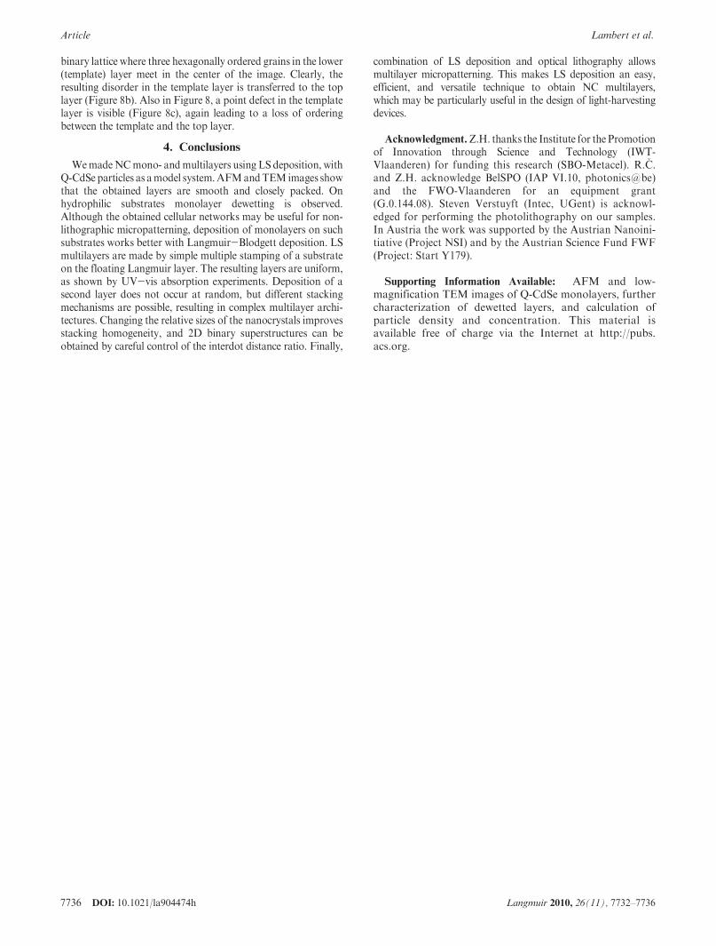
harvesting devices require multilayers containing different typesof nanocrystals.8 LSdeposition is not limited tomultilayers of onetype of nanocrystals and is thus an option for realizing suchapplications. Moreover, control of the interparticle distance ineach layer (by changing the particle diameter and/or ligandlength) may enable formation of ordered binary structures. Todemonstrate this, we deposited a monolayer of oleic acid-cappedFe3O4 nanoparticles (interparticle distance 9.3 nm) on a TEMgrid, followed by the deposition of a Q-CdSe monolayer(interparticle distance 4.8 nm). TEM images show not only thatit is possible to combine the two types ofmonolayers but also thatthe potential energy surface created by the bigger underlyingnanoparticles influences the positions of the nanoparticles in theupper layer (Figure 7a).With an interparticle distance ratio of
√3
the formation of a 2Dcrystalwhere the particles of the upper layeroccupy the A, B, and C positions of the lower layer should bepossible (Figure 7b,c). In this way, the small dots fill the gaps inthe monolayer of the large lower dots, with one excess small doton top of every large one. Although in our example the distanceratio is 10% larger than
√3, many of the Fe3O4 nanocrystals are
indeed surrounded by six CdSe particles, occupying B and C
positions and have oneCdSe particle on top.This suggests that ontop of making multilayers LS deposition may also lead to binary2D QD superlattices. The 3D counterparts of such superlatticesare usually produced by controlled evaporation of colloidal QDsuspensions.38-40 Although LS deposition is probably limited tosuperstructures with 2D symmetry, it has many advantages: itoffers easy control of particle stoichiometry, combination ofnanoparticles suspended in incompatible solvents, coating oflarge areas, and less control over atmospheric conditions isrequired during deposition. The ratio of the interdot distances,however, is still important, as large deviations from the ideal valueresult in unordered structures.
In areas where the underlying layer of larger particles is wellordered, few defects in the binary layer are observed. On the otherhand, defects in this first layer induce defects in the final binarylayer. This means that besides the interdot distance ratio, also thequality of the first layer is essential to the amount of stackingfaults in the binary layer. The first layer therefore really acts as atemplate layer. As an example, Figure 8 shows TEM images of a
Figure 6. AFM image (a) and profile (b) of a patterned Q-CdSebilayer.
Figure 7. TEM image (a), detail (b), and corresponding schematicrepresentation (c) of a Fe3O4/CdSe Langmuir-Schaefer binarylayer, with an interdot distance ratio around
√3. The smaller
Q-CdSe particles of the upper layer occupy the A, B, and Cpositions of the lower layer of larger Fe3O4.
Figure 8. TEM image (a) and details (b, c) Fe3O4/CdSeLangmuir-Schaefer binary layer. Defects in the binary layer aremainly induced through defects in the first layer, such as grainboundaries (b) and point defects (c).
(38) Overgaag, K.; Evers, W.; de Nijs, B.; Koole, R.; Meeldijk, J.;Vanmaekelbergh, D. J. Am. Chem. Soc. 2008, 130, 7833–7835.
(39) Lu, C.; Chen, Z.; O’Brien, S. Chem. Mater. 2008, 20, 3594–3600.(40) Shevchenko, E. V.; Talapin, D. V.; Kotov,N. A.; O’Brien, S.;Murray, C. B.
Nature 2006, 439, 55–59.
7736 DOI: 10.1021/la904474h Langmuir 2010, 26(11), 7732–7736
Article Lambert et al.
binary lattice where three hexagonally ordered grains in the lower(template) layer meet in the center of the image. Clearly, theresulting disorder in the template layer is transferred to the toplayer (Figure 8b). Also in Figure 8, a point defect in the templatelayer is visible (Figure 8c), again leading to a loss of orderingbetween the template and the top layer.
4. Conclusions
WemadeNCmono- andmultilayers using LS deposition, withQ-CdSe particles as amodel system.AFMandTEMimages showthat the obtained layers are smooth and closely packed. Onhydrophilic substrates monolayer dewetting is observed.Although the obtained cellular networks may be useful for non-lithographic micropatterning, deposition of monolayers on suchsubstrates works better with Langmuir-Blodgett deposition. LSmultilayers are made by simple multiple stamping of a substrateon the floating Langmuir layer. The resulting layers are uniform,as shown by UV-vis absorption experiments. Deposition of asecond layer does not occur at random, but different stackingmechanisms are possible, resulting in complex multilayer archi-tectures. Changing the relative sizes of the nanocrystals improvesstacking homogeneity, and 2D binary superstructures can beobtained by careful control of the interdot distance ratio. Finally,
combination of LS deposition and optical lithography allowsmultilayer micropatterning. This makes LS deposition an easy,efficient, and versatile technique to obtain NC multilayers,which may be particularly useful in the design of light-harvestingdevices.
Acknowledgment.Z.H. thanks the Institute for the Promotionof Innovation through Science and Technology (IWT-Vlaanderen) for funding this research (SBO-Metacel). R.�C.and Z.H. acknowledge BelSPO (IAP VI.10, photonics@be)and the FWO-Vlaanderen for an equipment grant(G.0.144.08). Steven Verstuyft (Intec, UGent) is acknowl-edged for performing the photolithography on our samples.In Austria the work was supported by the Austrian Nanoini-tiative (Project NSI) and by the Austrian Science Fund FWF(Project: Start Y179).
Supporting Information Available: AFM and low-magnification TEM images of Q-CdSe monolayers, furthercharacterization of dewetted layers, and calculation ofparticle density and concentration. This material isavailable free of charge via the Internet at http://pubs.acs.org.