labview -fpga module user manual
TRANSCRIPT
8/13/2019 LabVIEW -FPGA Module User Manual
http://slidepdf.com/reader/full/labview-fpga-module-user-manual 1/62
LabVIEW
TM
FPGA Module User Manual
FPGA Module User Manual
March 2004 Edition
Part Number 370690B-01
8/13/2019 LabVIEW -FPGA Module User Manual
http://slidepdf.com/reader/full/labview-fpga-module-user-manual 2/62
Support
Worldwide Technical Support and Product Information
ni.com
National Instruments Corporate Headquarters
11500 North Mopac Expressway Austin, Texas 78759-3504 USA Tel: 512 683 0100
Worldwide Offices
Australia 1800 300 800, Austria 43 0 662 45 79 90 0, Belgium 32 0 2 757 00 20, Brazil 55 11 3262 3599,
Canada (Calgary) 403 274 9391, Canada (Ottawa) 613 233 5949, Canada (Québec) 450 510 3055,
Canada (Toronto) 905 785 0085, Canada (Vancouver) 514 685 7530, China 86 21 6555 7838,
Czech Republic 420 224 235 774, Denmark 45 45 76 26 00, Finland 385 0 9 725 725 11,
France 33 0 1 48 14 24 24, Germany 49 0 89 741 31 30, Greece 30 2 10 42 96 427, India 91 80 51190000,
Israel 972 0 3 6393737, Italy 39 02 413091, Japan 81 3 5472 2970, Korea 82 02 3451 3400,
Malaysia 603 9131 0918, Mexico 001 800 010 0793, Netherlands 31 0 348 433 466,
New Zealand 0800 553 322, Norway 47 0 66 90 76 60, Poland 48 22 3390150, Portugal 351 210 311 210,
Russia 7 095 783 68 51, Singapore 65 6226 5886, Slovenia 386 3 425 4200, South Africa 27 0 11 805 8197,
Spain 34 91 640 0085, Sweden 46 0 8 587 895 00, Switzerland 41 56 200 51 51, Taiwan 886 2 2528 7227,
Thailand 662 992 7519, United Kingdom 44 0 1635 523545
For further support information, refer to the Technical Support and Professional Services appendix. To comment
on the documentation, send email to [email protected] .
© 2003–2004 National Instruments Corporation. All rights reserved.
8/13/2019 LabVIEW -FPGA Module User Manual
http://slidepdf.com/reader/full/labview-fpga-module-user-manual 3/62
Important Information
WarrantyThe media on which you receive National Instruments software are warranted not to fail to execute programming instructions, due to defects
in materials and workmanship, for a period of 90 days from date of shipment, as evidenced by receipts or other documentation. NationalInstruments will, at its option, repair or replace software media that do not execute programming instructions if National Instruments receivesnotice of such defects during the warranty period. National Instruments does not warrant that the operation of the software shall beuninterrupted or error free.
A Return Material Authorization (RMA) number must be obtained from the factory and clearly marked on the outside of the package beforeany equipment will be accepted for warranty work. National Instruments will pay the shipping costs of returning to the owner parts which arecovered by warranty.
National Instruments believes that the information in this document is accurate. The document has been carefully reviewed for technicalaccuracy. In the event that technical or typographical errors exist, National Instruments reserves the right to make changes to subsequenteditions of this document without prior notice to holders of this edition. The reader should consult National Instruments if errors are suspected.In no event shall National Instruments be liable for any damages arising out of or related to this document or the information contained in it.
EXCEPT AS SPECIFIED HEREIN, NATIONAL INSTRUMENTS MAKES NO WARRANTIES, EXPRESS OR IMPLIED, AND SPECIFICALLY DISCLAIMS ANY WARRANTY OF MERCHANTABILITY OR FITNESS FOR A PARTICULAR PURPOSE. CUSTOMER’S RIGHT TO RECOVER DAMAGES CAUSED BY FAULT OR NEGLIGENCE ON THE PART OF NATIONAL INSTRUMENTS SHALL BE LIMITED TO THE AMOUNT THERETOFORE PAID BY THE CUSTOMER. NATIONAL INSTRUMENTS WILL NOT BE LIABLE FOR DAMAGES RESULTING FROM LOSS OF DATA, PROFITS, USE OF PRODUCTS, OR INCIDENTAL OR CONSEQUENTIAL DAMAGES, EVEN IF ADVISED OF THE POSSIBILITY THEREOF. This limitation of the liability of National Instruments will apply regardless of the form of action, whether in contract or tort, includingnegligence. Any action against National Instruments must be brought within one year after the cause of action accrues. National Instruments
shall not be liable for any delay in performance due to causes beyond its reasonable control. The warranty provided herein does not coverdamages, defects, malfunctions, or service failures caused by owner’s failure to follow the National Instruments installation, operation, ormaintenance instructions; owner’s modification of the product; owner’s abuse, misuse, or negligent acts; and power failure or surges, fire,flood, accident, actions of third parties, or other events outside reasonable control.
CopyrightUnder the copyright laws, this publication may not be reproduced or transmitted in any form, electronic or mechanical, including photocopying,recording, storing in an information retrieval system, or translating, in whole or in part, without the prior written consent of NationalInstruments Corporation.
TrademarksLabVIEW™, National Instruments™, NI™, ni.com™, and NI Developer Zone™ are trademarks of National Instruments Corporation.
Product and company names mentioned herein are trademarks or trade names of their respective companies.
PatentsFor patents covering National Instruments products, refer to the appropriate location: Help»Patents in your software, the patents.txt fileon your CD, or ni.com/patents.
WARNING REGARDING USE OF NATIONAL INSTRUMENTS PRODUCTS(1) NATIONAL INSTRUMENTS PRODUCTS ARE NOT DESIGNED WITH COMPONENTS AND TESTING FOR A LEVEL OFRELIABILITY SUITABLE FOR USE IN OR IN CONNECTION WITH SURGICAL IMPLANTS OR AS CRITICAL COMPONENTS INANY LIFE SUPPORT SYSTEMS WHOSE FAILURE TO PERFORM CAN REASONABLY BE EXPECTED TO CAUSE SIGNIFICANTINJURY TO A HUMAN.
(2) IN ANY APPLICATION, INCLUDING THE ABOVE, RELIABILITY OF OPERATION OF THE SOFTWARE PRODUCTS CAN BEIMPAIRED BY ADVERSE FACTORS, INCLUDING BUT NOT LIMITED TO FLUCTUATIONS IN ELECTRICAL POWER SUPPLY,COMPUTER HARDWARE MALFUNCTIONS, COMPUTER OPERATING SYSTEM SOFTWARE FITNESS, FITNESS OF COMPILERSAND DEVELOPMENT SOFTWARE USED TO DEVELOP AN APPLICATION, INSTALLATION ERRORS, SOFTWARE ANDHARDWARE COMPATIBILITY PROBLEMS, MALFUNCTIONS OR FAILURES OF ELECTRONIC MONITORING OR CONTROLDEVICES, TRANSIENT FAILURES OF ELECTRONIC SYSTEMS (HARDWARE AND/OR SOFTWARE), UNANTICIPATED USES ORMISUSES, OR ERRORS ON THE PART OF THE USER OR APPLICATIONS DESIGNER (ADVERSE FACTORS SUCH AS THESE AREHEREAFTER COLLECTIVELY TERMED “SYSTEM FAILURES”). ANY APPLICATION WHERE A SYSTEM FAILURE WOULD
CREATE A RISK OF HARM TO PROPERTY OR PERSONS (INCLUDING THE RISK OF BODILY INJURY AND DEATH) SHOULDNOT BE RELIANT SOLELY UPON ONE FORM OF ELECTRONIC SYSTEM DUE TO THE RISK OF SYSTEM FAILURE. TO AVOIDDAMAGE, INJURY, OR DEATH, THE USER OR APPLICATION DESIGNER MUST TAKE REASONABLY PRUDENT STEPS TOPROTECT AGAINST SYSTEM FAILURES, INCLUDING BUT NOT LIMITED TO BACK-UP OR SHUT DOWN MECHANISMS.BECAUSE EACH END-USER SYSTEM IS CUSTOMIZED AND DIFFERS FROM NATIONAL INSTRUMENTS' TESTINGPLATFORMS AND BECAUSE A USER OR APPLICATION DESIGNER MAY USE NATIONAL INSTRUMENTS PRODUCTS INCOMBINATION WITH OTHER PRODUCTS IN A MANNER NOT EVALUATED OR CONTEMPLATED BY NATIONALINSTRUMENTS, THE USER OR APPLICATION DESIGNER IS ULTIMATELY RESPONSIBLE FOR VERIFYING AND VALIDATINGTHE SUITABILITY OF NATIONAL INSTRUMENTS PRODUCTS WHENEVER NATIONAL INSTRUMENTS PRODUCTS AREINCORPORATED IN A SYSTEM OR APPLICATION, INCLUDING, WITHOUT LIMITATION, THE APPROPRIATE DESIGN,PROCESS AND SAFETY LEVEL OF SUCH SYSTEM OR APPLICATION.
8/13/2019 LabVIEW -FPGA Module User Manual
http://slidepdf.com/reader/full/labview-fpga-module-user-manual 4/62
© National Instruments Corporation v FPGA Module User Manual
Contents
About This Manual
Conventions ................................................................................................................... ixRelated Documentation..................................................................................................x
Chapter 1Introduction
Custom Hardware from LabVIEW................................................................................1-1
Additional Advantages of the FPGA Module................................................................1-2
FPGA Module Application Development .....................................................................1-2
Execution Targets............................................................................................1-2
Execution of FPGA VIs...................................................................................1-3
Communication with FPGA VIs .....................................................................1-3Interactive Front Panel Communication ........................................... 1-3
Programmatic FPGA Interface Communication...............................1-5
FPGA Module Examples ...............................................................................................1-7
Chapter 2Creating FPGA VIs
Targeting FPGA Devices...............................................................................................2-1
Managing FPGA VIs with the Embedded Project Manager..........................................2-1
Utilizing FPGA Space ...................................................................................................2-3
Performing Basic I/O ..................................................................................................... 2-4
Analog I/O.......................................................................................................2-5
Analog Input .....................................................................................2-5
Analog Output...................................................................................2-5
Digital I/O........................................................................................................2-6
Timing FPGA VIs..........................................................................................................2-7
Creating Timed I/O Applications .................................................................... 2-7
Creating Delays between Events.....................................................................2-8
Measuring Time between Events .................................................................... 2-8
Executing Code in a Single FPGA Device Clock Cycle.................................2-9
Customizing I/O.............................................................................................................2-11Creating Triggers.............................................................................................2-12
Creating Counters............................................................................................2-13
Using Parallel Operations ..............................................................................................2-15
Parallel Operations on the FPGA .................................................................... 2-15
SubVIs on the FPGA.......................................................................................2-17
Transferring Data Among Parallel Loops .......................................................2-18
8/13/2019 LabVIEW -FPGA Module User Manual
http://slidepdf.com/reader/full/labview-fpga-module-user-manual 5/62
Contents
FPGA Module User Manual vi ni.com
Understanding How to Program FPGA VIs.................................................................. 2-19
Restricted and Unavailable VIs and Functions ............................................... 2-19
Mathematical Operations ................................................................................ 2-19
Arrays.............................................................................................................. 2-21
Memory........................................................................................................... 2-21
Using HDL Code in FPGA VIs ...................................................................... 2-22Controlling I/O Power-On States .................................................................................. 2-22
Communicating with a Host VI..................................................................................... 2-23
Interrupt-Based Communication..................................................................... 2-24
Chapter 3Managing Shared Resources
Resource Contention and Arbitration............................................................................ 3-1
Jitter ............................................................................................................................... 3-3
Arbitration Options........................................................................................................ 3-4
Normal ............................................................................................................ 3-4Normal (Optimize for Single Accessor) ......................................................... 3-5
None................................................................................................................ 3-5
Available Arbitration Options for Specific Resources ................................... 3-5
Timing ........................................................................................................................... 3-7
FPGA Utilization........................................................................................................... 3-8
Chapter 4Running FPGA VIs
Compiling FPGA VIs .................................................................................................... 4-1
Compiling FPGA VIs Using the LabVIEW FPGA Compile Server .............. 4-2
Compiling on a Remote Computer ................................................................. 4-2
Managing Compilation Files........................................................................... 4-3
Using Compiled FPGA VI Options............................................................................... 4-3
Changing the FPGA Device Clock Rate......................................................... 4-3
Configuring FPGA VIs to Run Automatically ............................................... 4-4
Downloading Compiled FPGA VIs to the FPGA Device ............................................. 4-4
Running Compiled FPGA VIs....................................................................................... 4-5
Running FPGA VIs at Power On .................................................................................. 4-5
Setting Target Configurations ....................................................................................... 4-6
8/13/2019 LabVIEW -FPGA Module User Manual
http://slidepdf.com/reader/full/labview-fpga-module-user-manual 6/62
Contents
© National Instruments Corporation vii FPGA Module User Manual
Chapter 5Debugging FPGA VIs
Testing a VI Before Compiling ..................................................................................... 5-1
Building Debugging into an FPGA VI ..........................................................................5-2
Adding Indicators ............................................................................................5-2Adding I/O.......................................................................................................5-2
Appendix ATechnical Support and Professional Services
Glossary
8/13/2019 LabVIEW -FPGA Module User Manual
http://slidepdf.com/reader/full/labview-fpga-module-user-manual 7/62
© National Instruments Corporation ix FPGA Module User Manual
About This Manual
This manual describes the LabVIEW FPGA Module software and
techniques for building applications in LabVIEW with the FPGA Module.
Use this manual to learn about FPGA Module programming features to
help you build VIs that run on National Instruments Reconfigurable I/O
(RIO) devices, also known as FPGA devices, and VIs to communicate with
FPGA devices.
Refer to the FPGA Interface User Guide for information about
communicating with the FPGA device from a host computer.
Conventions
The following conventions appear in this manual:
» The » symbol leads you through nested menu items and dialog box options
to a final action. The sequence File»Page Setup»Options directs you to
pull down the File menu, select the Page Setup item, and select Options
from the last dialog box.
This icon denotes a tip, which alerts you to advisory information.
This icon denotes a note, which alerts you to important information.
bold Bold text denotes items that you must select or click in the software, such
as menu items and dialog box options. Bold text also denotes parameter
names and palette names.
italic Italic text denotes variables, emphasis, a cross reference, or an introduction
to a key concept. This font also denotes text that is a placeholder for a word
or value that you must supply.
monospace Text in this font denotes text or characters that you should enter from the
keyboard, sections of code, programming examples, and syntax examples.
This font is also used for the proper names of disk drives, paths, directories,
programs, subprograms, subroutines, device names, functions, operations,
variables, filenames, and extensions.
monospace italic Italic text in this font denotes text that is a placeholder for a word or value
that you must supply.
8/13/2019 LabVIEW -FPGA Module User Manual
http://slidepdf.com/reader/full/labview-fpga-module-user-manual 8/62
8/13/2019 LabVIEW -FPGA Module User Manual
http://slidepdf.com/reader/full/labview-fpga-module-user-manual 9/62
© National Instruments Corporation 1-1 FPGA Module User Manual
1Introduction
With the LabVIEW FPGA Module and LabVIEW, you can create VIs
that run on National Instruments Reconfigurable I/O (RIO) devices.
Reconfigurable I/O devices, also known as FPGA devices, contain a
reconfigurable FPGA (Field-Programmable Gate Array) surrounded by
fixed I/O resources. Depending on the specific FPGA device, fixed
I/O resources can include analog and digital resources—such as
analog-to-digital converters (ADCs) and digital-to-analog converters
(DACs)—that you can control from the FPGA.
With the FPGA Module, you configure the behavior of the reconfigurableFPGA to match the requirements of a specific measurement and control
system. The VI you create to run on an FPGA device is called the FPGA VI .
Use the FPGA Module to write FPGA VIs. When you download the FPGA
VI to the FPGA, you are programming the functionality of the FPGA
device. Each new FPGA VI you create and download is a custom timing,
triggering, and I/O solution.
Custom Hardware from LabVIEW
When standard hardware did not meet your requirements for a specific
application prior to the FPGA Module, you had to create a custom
hardware design using low-level hardware description languages. With the
FPGA Module, you do not need to know a hardware description language
to design a specific hardware solution—you just need LabVIEW. With the
FPGA Module, you can design and rapidly develop hardware components
with the power of LabVIEW graphical programming.
The FPGA Module is ideal for programming applications that require
functionality such as the following:
• Custom I/O—Modified digital and analog lines with custom counters,encoders, and pulse width modulators (PWMs)
• Onboard decision making—Control, digital filtering, and Boolean
decisions
• Resource synchronization—Precise timing of FPGA device
resources, such as analog input (AI), analog output (AO), digital input
8/13/2019 LabVIEW -FPGA Module User Manual
http://slidepdf.com/reader/full/labview-fpga-module-user-manual 10/62
Chapter 1 Introduction
FPGA Module User Manual 1-2 ni.com
and output (DIO), counters, and PWMs, as well as synchronization
among multiple devices
Additional Advantages of the FPGA Module
The FPGA Module expands the functionality of LabVIEW solutions. For
example, you can design FPGA VIs that allow the FPGA device to operate
independently of the rest of the system. You can create robust FPGA VIs
that use the ability to operate independently and continue to run even if the
host computer —the computer that controls and monitors the FPGA
device—crashes. Furthermore, you can design the FPGA VI to store data
on the FPGA until the host computer can retrieve the data.
Another advantage of the FPGA Module is parallel execution of block
diagram operations in an FPGA VI. Portions of the block diagram that do
not depend on other portions execute in parallel on the FPGA device. Forexample, multiple independent While Loops on a block diagram each have
independent portions of hardware. Therefore, the multiple independent
While Loops run simultaneously on the FPGA device.
FPGA Module Application Development
FPGA Module applications range from a single FPGA VI running on an
FPGA device to large LabVIEW solutions that include multiple FPGA
devices, the LabVIEW Real-Time Module, and LabVIEW for Windows.
In any case, you need to create the FPGA VI that runs on the FPGA device.To create an FPGA VI, first select the FPGA device as the execution target
in LabVIEW. An execution target is any location—including FPGA
devices, RT targets, or the development computer—on which you can
run a VI.
Execution TargetsBy default, LabVIEW selects the development computer as the execution
target. You must change the execution target to access the FPGA Module
palettes, VIs, functions, and development tools. To change the execution
target from the LabVIEW dialog box, select an FPGA device from theExecution Target pull-down menu. The Embedded Project Manager
window appears. Refer to Chapter 2, Creating FPGA VIs, for information
about creating and managing FPGA VIs using the Embedded Project
Manager.
8/13/2019 LabVIEW -FPGA Module User Manual
http://slidepdf.com/reader/full/labview-fpga-module-user-manual 11/62
Chapter 1 Introduction
© National Instruments Corporation 1-3 FPGA Module User Manual
Even if the target device is not present, you still can target an FPGA device
to develop an FPGA VI. If you are currently working on a VI and you want
to change the execution target, you can select Target»Switch Execution
Target from the Embedded Project Manager window to set the execution
target. Refer to Chapter 2, Creating FPGA VIs, for information about good
programming techniques and the VIs, functions, and tools in the FPGAModule that you need to create efficient FPGA VIs.
Execution of FPGA VIsAfter you create an FPGA VI with the FPGA Module VIs, functions,
and tools, use LabVIEW to compile and download the FPGA VI to the
FPGA device. As you do with any other VI, click the Run button in the
Embedded Project Manager window to automatically compile,
download, and run the FPGA VI on the execution target, which in this
case is the FPGA device. Refer to Chapter 4, Running FPGA VIs, for
information about compiling, downloading, and running FPGA VIs onthe FPGA device.
Communication with FPGA VIsAfter you have an FPGA VI running on the FPGA device, you need a
way to communicate with that VI. Depending on the application
requirements, you can communicate with the FPGA VI interactively or
programmatically. Use Interactive Front Panel Communication to
communicate with the FPGA VI directly from the front panel of the
FPGA VI. Use Programmatic FPGA Interface Communication to
communicate with the FPGA VI from a VI running on the host computer.
The VI running on the host computer is called the host VI .
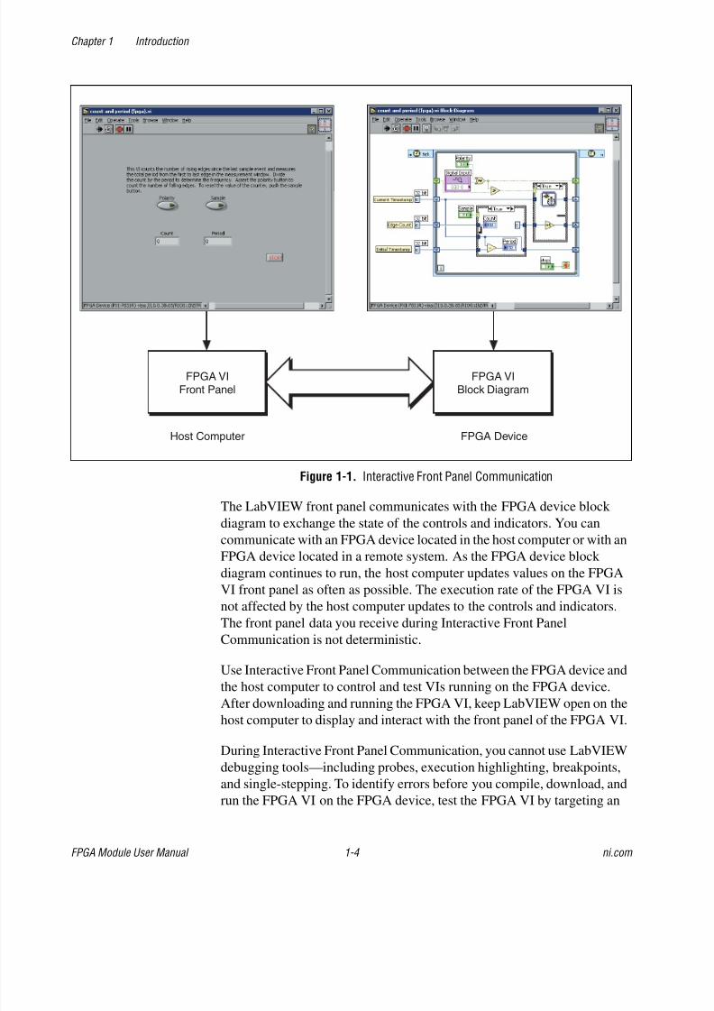
Interactive Front Panel CommunicationUse Interactive Front Panel Communication to communicate with an
FPGA VI running on an FPGA device with no additional programming.
With Interactive Front Panel Communication, the host computer displays
the FPGA VI front panel and the FPGA device executes the FPGA VI block
diagram, as shown in Figure 1-1.
8/13/2019 LabVIEW -FPGA Module User Manual
http://slidepdf.com/reader/full/labview-fpga-module-user-manual 12/62
Chapter 1 Introduction
FPGA Module User Manual 1-4 ni.com
Figure 1-1. Interactive Front Panel Communication
The LabVIEW front panel communicates with the FPGA device block
diagram to exchange the state of the controls and indicators. You cancommunicate with an FPGA device located in the host computer or with an
FPGA device located in a remote system. As the FPGA device block
diagram continues to run, the host computer updates values on the FPGA
VI front panel as often as possible. The execution rate of the FPGA VI is
not affected by the host computer updates to the controls and indicators.
The front panel data you receive during Interactive Front Panel
Communication is not deterministic.
Use Interactive Front Panel Communication between the FPGA device and
the host computer to control and test VIs running on the FPGA device.
After downloading and running the FPGA VI, keep LabVIEW open on the
host computer to display and interact with the front panel of the FPGA VI.
During Interactive Front Panel Communication, you cannot use LabVIEW
debugging tools—including probes, execution highlighting, breakpoints,
and single-stepping. To identify errors before you compile, download, and
run the FPGA VI on the FPGA device, test the FPGA VI by targeting an
FPGA VIFront Panel
Host Computer FPGA Device
FPGA VIBlock Diagram
8/13/2019 LabVIEW -FPGA Module User Manual
http://slidepdf.com/reader/full/labview-fpga-module-user-manual 13/62
Chapter 1 Introduction
© National Instruments Corporation 1-5 FPGA Module User Manual
FPGA device emulator. An emulator is an execution target that simulates
the behavior of the FPGA VI running on the FPGA device. Refer to
Chapter 5, Debugging FPGA VIs, for more information about testing
FPGA VIs with emulators.
Programmatic FPGA Interface CommunicationWith Programmatic FPGA Interface Communication, you
programmatically monitor and control an FPGA VI with a separate host VI
running on the host computer. You might write a host VI to send
information between the host computer and the FPGA device for the
following reasons:
• You want to do more data processing than you can fit on the FPGA.
• You need to perform operations not available on the FPGA device,
such as floating-point arithmetic.
• You want to create a multitiered application with the FPGA device asa component of a larger system.
• You want to log data.
• You want to run multiple VIs on the host computer. You cannot use
LabVIEW on the host computer for any other task when you target an
FPGA device or RT target while using Interactive Front Panel
Communication.
• You want to control the timing and sequencing of data transfer.
• You want to control which components are visible on the front panel
because some controls and indicators might be more important forcommunication than others.
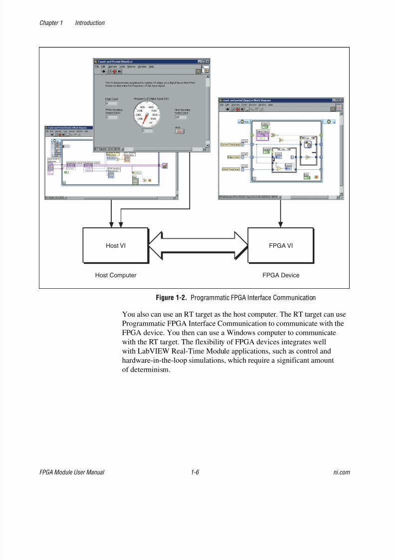
When you use Programmatic FPGA Interface Communication, the FPGA
VI runs on the FPGA device, and the host VI runs on the host computer, as
shown in Figure 1-2. Use the FPGA Interface functions available when you
target LabVIEW for Windows or an RT target to create a host VI that
communicates with the FPGA VI and performs other required functions.
Refer to the FPGA Interface User Guide for information about creating
host VIs.
8/13/2019 LabVIEW -FPGA Module User Manual
http://slidepdf.com/reader/full/labview-fpga-module-user-manual 14/62
Chapter 1 Introduction
FPGA Module User Manual 1-6 ni.com
Figure 1-2. Programmatic FPGA Interface Communication
You also can use an RT target as the host computer. The RT target can use
Programmatic FPGA Interface Communication to communicate with the
FPGA device. You then can use a Windows computer to communicate
with the RT target. The flexibility of FPGA devices integrates well
with LabVIEW Real-Time Module applications, such as control and
hardware-in-the-loop simulations, which require a significant amount
of determinism.
Host VI
Host Computer FPGA Device
FPGA VI
8/13/2019 LabVIEW -FPGA Module User Manual
http://slidepdf.com/reader/full/labview-fpga-module-user-manual 15/62
Chapter 1 Introduction
© National Instruments Corporation 1-7 FPGA Module User Manual
FPGA Module Examples
The FPGA Module includes example FPGA VIs and example host VIs
located in the examples\FPGA directory. The FPGA Module examples are
divided into categories such as Getting Started, Timing and Triggering,
Counters, and so on. The FPGA Module also includes VI templates to help
you create specific FPGA VI solutions.
Begin with the Getting Started examples to learn about simplified functions
based on actual application VIs. The Getting Started examples highlight
key concepts, such as communication between the host VI and the FPGA
VI as well as simplified timing, triggering, and data transfer. Continue
through the other categories of FPGA Module examples for more detailed
information.
Select Help»Find Examples to search the development computer and
ni.com for FPGA Module examples.
8/13/2019 LabVIEW -FPGA Module User Manual
http://slidepdf.com/reader/full/labview-fpga-module-user-manual 16/62
© National Instruments Corporation 2-1 FPGA Module User Manual
2Creating FPGA VIs
This chapter describes how to create an FPGA VI for an FPGA device.
You will learn how to perform common tasks such as I/O, timing, and
triggering, as well as more advanced tasks such as using parallel
operations.
Targeting FPGA Devices
The LabVIEW FPGA Module provides the same graphical programming
environment for the creation of FPGA VIs as LabVIEW does for standardVIs. The LabVIEW graphical programming environment includes front
panels and block diagrams, powerful editing tools, and a wide range of
included functions.
When you target LabVIEW to an FPGA device, you have access only to the
LabVIEW VIs and functions that make sense on the FPGA device. For
example, a typical FPGA device does not have access to a disk drive, so File
I/O functions are not available on the Functions palette when you target
that device. The LabVIEW VIs and functions available when you target an
FPGA device have the same behavior and functionality in FPGA VIs as in
VIs created for Windows. In addition to the subset of the standard
LabVIEW VIs and functions, the FPGA Module provides FPGA
device-specific VIs and functions. Refer to the LabVIEW Help, available by
selecting Help»VI, Function, & How-To Help, for information about VIs
and functions available when you target an FPGA device.
Tip You can identify FPGA Device I/O functions on the palettes by their purple borders.
Managing FPGA VIs with the
Embedded Project ManagerUse the Embedded Project Manager to manage groups of FPGA VIs and
the common information among the VIs, such as I/O resource aliases. You
must add an FPGA VI to a LabVIEW Embedded Project (LEP) file to
configure the FPGA Device I/O functions and to compile and run the VI.
8/13/2019 LabVIEW -FPGA Module User Manual
http://slidepdf.com/reader/full/labview-fpga-module-user-manual 17/62
Chapter 2 Creating FPGA VIs
FPGA Module User Manual 2-2 ni.com
Select an FPGA device from the Execution Target pull-down menu in
the LabVIEW dialog box to launch the Embedded Project Manager
window. You also can open the Embedded Project Manager window by
selecting Embedded Project Manager from the Open pull-down menu or
Tools»Embedded Project Manager from the LabVIEW dialog box.
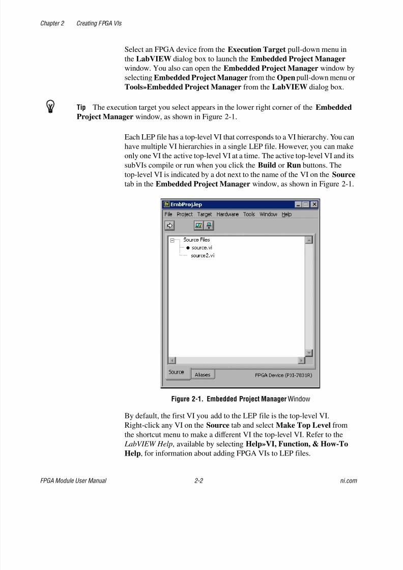
Tip The execution target you select appears in the lower right corner of the Embedded
Project Manager window, as shown in Figure 2-1.
Each LEP file has a top-level VI that corresponds to a VI hierarchy. You can
have multiple VI hierarchies in a single LEP file. However, you can make
only one VI the active top-level VI at a time. The active top-level VI and its
subVIs compile or run when you click the Build or Run buttons. The
top-level VI is indicated by a dot next to the name of the VI on the Source
tab in the Embedded Project Manager window, as shown in Figure 2-1.
Figure 2-1. Embedded Project Manager Window
By default, the first VI you add to the LEP file is the top-level VI.
Right-click any VI on the Source tab and select Make Top Level from
the shortcut menu to make a different VI the top-level VI. Refer to the
LabVIEW Help, available by selecting Help»VI, Function, & How-To
Help, for information about adding FPGA VIs to LEP files.
8/13/2019 LabVIEW -FPGA Module User Manual
http://slidepdf.com/reader/full/labview-fpga-module-user-manual 18/62
Chapter 2 Creating FPGA VIs
© National Instruments Corporation 2-3 FPGA Module User Manual
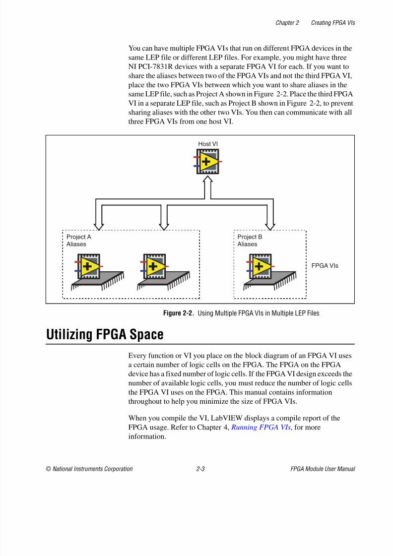
You can have multiple FPGA VIs that run on different FPGA devices in the
same LEP file or different LEP files. For example, you might have three
NI PCI-7831R devices with a separate FPGA VI for each. If you want to
share the aliases between two of the FPGA VIs and not the third FPGA VI,
place the two FPGA VIs between which you want to share aliases in the
same LEP file, such as Project A shown in Figure 2-2. Place the third FPGAVI in a separate LEP file, such as Project B shown in Figure 2-2, to prevent
sharing aliases with the other two VIs. You then can communicate with all
three FPGA VIs from one host VI.
Figure 2-2. Using Multiple FPGA VIs in Multiple LEP Files
Utilizing FPGA Space
Every function or VI you place on the block diagram of an FPGA VI uses
a certain number of logic cells on the FPGA. The FPGA on the FPGA
device has a fixed number of logic cells. If the FPGA VI design exceeds the
number of available logic cells, you must reduce the number of logic cellsthe FPGA VI uses on the FPGA. This manual contains information
throughout to help you minimize the size of FPGA VIs.
When you compile the VI, LabVIEW displays a compile report of the
FPGA usage. Refer to Chapter 4, Running FPGA VIs, for more
information.
Project AAliases
Project BAliases
Host VI
FPGA VIs
8/13/2019 LabVIEW -FPGA Module User Manual
http://slidepdf.com/reader/full/labview-fpga-module-user-manual 19/62
Chapter 2 Creating FPGA VIs
FPGA Module User Manual 2-4 ni.com
Performing Basic I/O
The FPGA Device I/O functions correspond to the fixed I/O resources on
the FPGA device. Fixed resources can include analog input, digital output,
and so on. When the FPGA VI runs on the FPGA device, it performs the
I/O operations in hardware. For example, the Analog Input function
initiates a conversion on the analog-to-digital converter (ADC) and returns
the result to the FPGA VI. Because FPGA VIs run directly on the FPGA,
you do not need driver calls or experience software delays.
Each FPGA Device I/O function corresponds to a specific type of fixed I/O
resource. An FPGA device might include multiple I/O resources of the
same type. Each individual I/O resource is a terminal on the FPGA device.
You can configure the FPGA Device I/O functions to read or write to as
many terminals as are available on the FPGA device. For example, you can
use the Analog Input function to read the data input on any of the analoginput terminals on the FPGA device.
Complete the following steps to configure an FPGA Device I/O function.
1. Create or open an LEP file.
2. Create or open a VI associated with the LEP file and open the block
diagram.
3. Place the appropriate FPGA Device I/O function on the block diagram.
The FPGA Module offers functions for analog input and output, digital
input and output, and digital port input and output.
4. Double-click or right-click the function on the block diagram and
select Properties from the shortcut menu.
Notice that the Configure dialog box contains one fixed I/O resource
in the Preview listbox.
5. Select an available fixed I/O resource with which you want to associate
inputs or outputs from the Terminal listbox on the General page.
Refer to the hardware documentation for information about terminals
and their connector assignments.
6. Type a name in the Alias listbox to specify an Alias for the fixed I/O
resource. You also can add, edit, or delete aliases in the Alias Manager dialog box, available by selecting Hardware»Alias Manager in the
Embedded Project Manager window. LabVIEW uses the terminal
name as the default Alias.

8/13/2019 LabVIEW -FPGA Module User Manual
http://slidepdf.com/reader/full/labview-fpga-module-user-manual 20/62
Chapter 2 Creating FPGA VIs
© National Instruments Corporation 2-5 FPGA Module User Manual
7. To associate more inputs or outputs with a fixed I/O resource, click the
Add Input or Add Output button and configure the fixed I/O resource
as you did in the previous step.
8. Click the OK button to save the I/O configuration and close the
Configure dialog box.
Analog I/O
Analog InputThe Analog Input function initiates a conversion, waits for the result, then
returns the binary representation of the voltage as a signed integer. The size
of the data type of the result varies by execution target. Typically you create
the FPGA VI to use the binary representation for operations within the
FPGA VI. You also can pass the binary representation back to the host VI
and convert the binary representation back to a voltage.
The equation you use to convert the binary representation back to an actual
voltage depends on the specific FPGA device. Refer to the hardware
documentation for more information. For example, with an NI PXI-7831R
device, use the following equation to convert the binary representation to
voltage:
Note Avoid executing this calculation in the FPGA VI because the FPGA only supportsinteger operations. Also, performing the equation on the FPGA uses additional space on
the FPGA. Refer to the Mathematical Operations section of this chapter for more
information.
Analog OutputThe Analog Output function writes the binary representation of the voltage
as a 16-bit signed integer to the digital-to-analog converter (DAC), which
sets the analog output voltage. You can generate voltage information in two
sources—the host VI or the FPGA VI. Typically the host VI converts the
voltage to a signed 16-bit binary representation before writing the value tothe FPGA VI. If the FPGA VI determines the voltage, typically the
FPGA VI performs the calculations using 16-bit binary representations.
In both cases, the DAC passes the binary representation out as a voltage.
Input Voltage Binary Code
32768---------------------------------- 10.0 V×=
8/13/2019 LabVIEW -FPGA Module User Manual
http://slidepdf.com/reader/full/labview-fpga-module-user-manual 21/62
Chapter 2 Creating FPGA VIs
FPGA Module User Manual 2-6 ni.com
The equation you use to convert a voltage to a binary representation
depends on the specific FPGA device. Refer to the hardware
documentation for more information. For example, with an NI PXI-7831R
device, use the following equation to convert the voltage to the binary
representation:
Note Avoid executing this calculation in the FPGA VI because the FPGA only supports
integer operations. Also, performing the equation on the FPGA uses additional space on
the FPGA. Refer to the Mathematical Operations section for more information.
Digital I/OYou can treat digital resources as individual lines or as predefined groups
of eight digital lines, also known as ports. A terminal is either an individual
digital line or a digital port depending on which FPGA Device I/O function
you use. You can perform both digital input and digital output on any
digital terminal. Refer to the LabVIEW Help, available by selecting
Help»VI, Function, & How-To Help, for information about specific
FPGA Device I/O functions and port assignments.
Use the Digital Input and Digital Port Input functions to read the state of a
digital terminal or digital port. The state of the digital terminal is commonly
determined by an external signal, such as the output generated by an
external device. Use the Digital Output and Digital Port Output functionsto set the state of a digital terminal or port. You can use the Digital Input
functions to verify the state of the same terminal to which the Digital
Output function writes.
Note If you have used a terminal for output, you must use the Digital Enable or Digital
Port Enable function to disable the terminal for output before the Digital Input function can
read the state of an external signal.
The Digital Output and Digital Port Output functions both write the data
and enable the terminal for output. You also can use the Digital Data and
Digital Port Data functions, which write data to a terminal but do not enable
the output. Use the Digital Enable and Digital Port Enable functions to
enable the digital terminal, which allows the data to be driven out. For
example, you might have one portion of the block diagram continuously
generating an internal signal. Use a Digital Enable or Digital Port Enable
function in another portion of the block diagram to independently control
when the internal signal is actually driven out to an external device.
Binary Code Output Voltage 32768×
10.0 V--------------------------------------------------------------=
8/13/2019 LabVIEW -FPGA Module User Manual
http://slidepdf.com/reader/full/labview-fpga-module-user-manual 22/62
Chapter 2 Creating FPGA VIs
© National Instruments Corporation 2-7 FPGA Module User Manual
Timing FPGA VIs
Every VI or function you place in an FPGA VI takes a certain amount of
time to execute. You can allow operations to occur at the rate determined
by the dataflow without additional programming. If you want to control or
measure the execution timing, use the Time & Dialog VIs. You also can use
the Time & Dialog VIs to create custom I/O such as counters and triggers.
Creating Timed I/O ApplicationsApplications often require the I/O to execute at a specific frequency. For
example, the algorithms used in control loops typically require the inputs
to be sampled at a known rate. Use the Loop Timer VI in a While Loop to
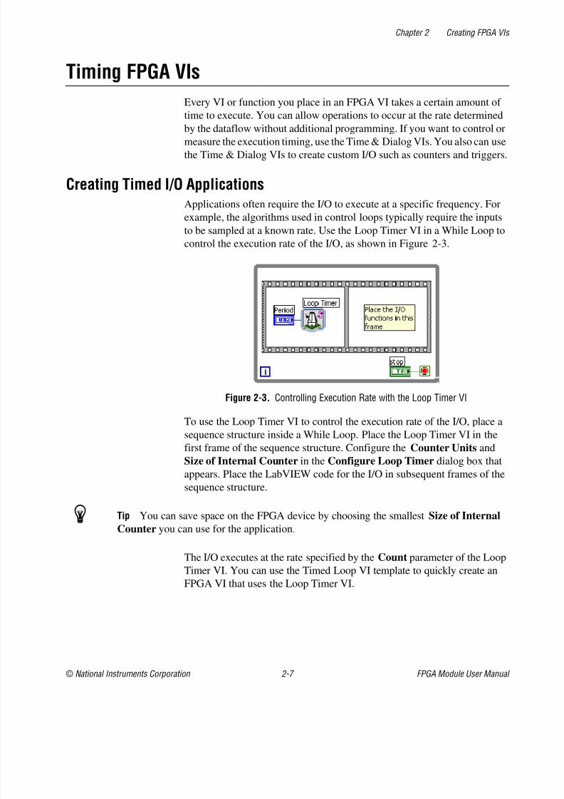
control the execution rate of the I/O, as shown in Figure 2-3.
Figure 2-3. Controlling Execution Rate with the Loop Timer VI
To use the Loop Timer VI to control the execution rate of the I/O, place a
sequence structure inside a While Loop. Place the Loop Timer VI in the
first frame of the sequence structure. Configure the Counter Units and
Size of Internal Counter in the Configure Loop Timer dialog box that
appears. Place the LabVIEW code for the I/O in subsequent frames of the
sequence structure.
Tip You can save space on the FPGA device by choosing the smallest Size of Internal
Counter you can use for the application.
The I/O executes at the rate specified by the Count parameter of the Loop
Timer VI. You can use the Timed Loop VI template to quickly create an
FPGA VI that uses the Loop Timer VI.
8/13/2019 LabVIEW -FPGA Module User Manual
http://slidepdf.com/reader/full/labview-fpga-module-user-manual 23/62
Chapter 2 Creating FPGA VIs
FPGA Module User Manual 2-8 ni.com
The first call of the Loop Timer VI does not result in any wait or delay
because it establishes a reference time stamp for subsequent calls. After the
first call of the Loop Timer VI, subsequent calls of the Loop Timer VI do
not return until the time specified by the Count parameter has elapsed since
the previous call. If the time specified by the Count parameter is less than
the time it takes the FPGA device to execute the code in the While Loop,the Loop Timer VI returns immediately and establishes a new reference
time stamp for subsequent calls.
Refer to the LabVIEW Help, available by selecting Help»VI, Function,
& How-To Help, for more information about the Loop Timer VI.
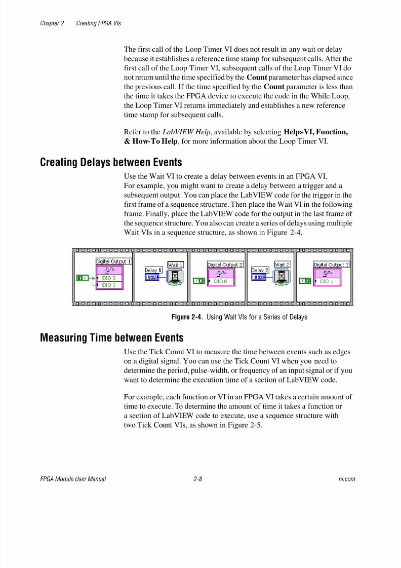
Creating Delays between EventsUse the Wait VI to create a delay between events in an FPGA VI.
For example, you might want to create a delay between a trigger and a
subsequent output. You can place the LabVIEW code for the trigger in thefirst frame of a sequence structure. Then place the Wait VI in the following
frame. Finally, place the LabVIEW code for the output in the last frame of
the sequence structure. You also can create a series of delays using multiple
Wait VIs in a sequence structure, as shown in Figure 2-4.
Figure 2-4. Using Wait VIs for a Series of Delays
Measuring Time between EventsUse the Tick Count VI to measure the time between events such as edges
on a digital signal. You can use the Tick Count VI when you need to
determine the period, pulse-width, or frequency of an input signal or if you
want to determine the execution time of a section of LabVIEW code.
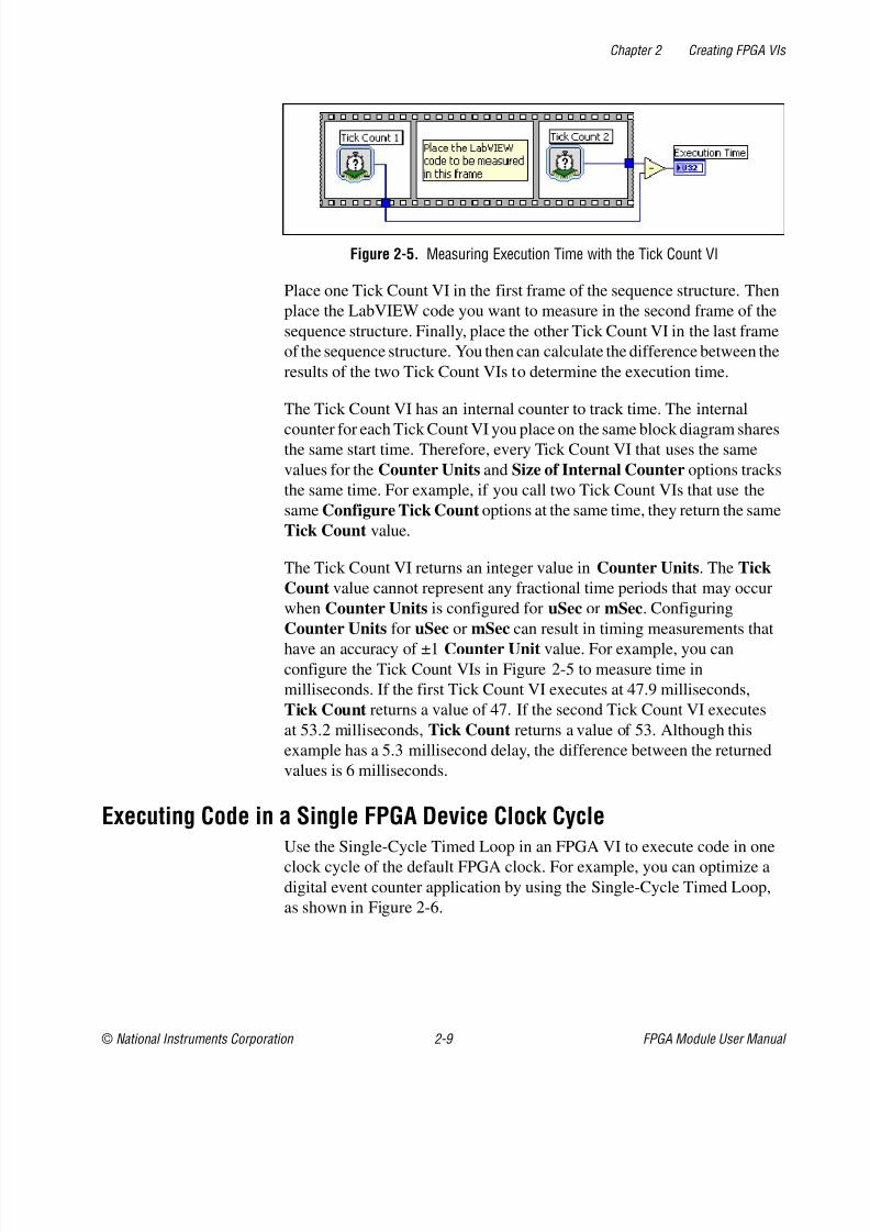
For example, each function or VI in an FPGA VI takes a certain amount of
time to execute. To determine the amount of time it takes a function or
a section of LabVIEW code to execute, use a sequence structure with
two Tick Count VIs, as shown in Figure 2-5.
8/13/2019 LabVIEW -FPGA Module User Manual
http://slidepdf.com/reader/full/labview-fpga-module-user-manual 24/62
Chapter 2 Creating FPGA VIs
© National Instruments Corporation 2-9 FPGA Module User Manual
Figure 2-5. Measuring Execution Time with the Tick Count VI
Place one Tick Count VI in the first frame of the sequence structure. Then
place the LabVIEW code you want to measure in the second frame of the
sequence structure. Finally, place the other Tick Count VI in the last frame
of the sequence structure. You then can calculate the difference between the
results of the two Tick Count VIs to determine the execution time.
The Tick Count VI has an internal counter to track time. The internal
counter for each Tick Count VI you place on the same block diagram sharesthe same start time. Therefore, every Tick Count VI that uses the same
values for the Counter Units and Size of Internal Counter options tracks
the same time. For example, if you call two Tick Count VIs that use the
same Configure Tick Count options at the same time, they return the same
Tick Count value.
The Tick Count VI returns an integer value in Counter Units. The Tick
Count value cannot represent any fractional time periods that may occur
when Counter Units is configured for uSec or mSec. Configuring
Counter Units for uSec or mSec can result in timing measurements that
have an accuracy of ±1 Counter Unit value. For example, you can
configure the Tick Count VIs in Figure 2-5 to measure time in
milliseconds. If the first Tick Count VI executes at 47.9 milliseconds,
Tick Count returns a value of 47. If the second Tick Count VI executes
at 53.2 milliseconds, Tick Count returns a value of 53. Although this
example has a 5.3 millisecond delay, the difference between the returned
values is 6 milliseconds.
Executing Code in a Single FPGA Device Clock Cycle
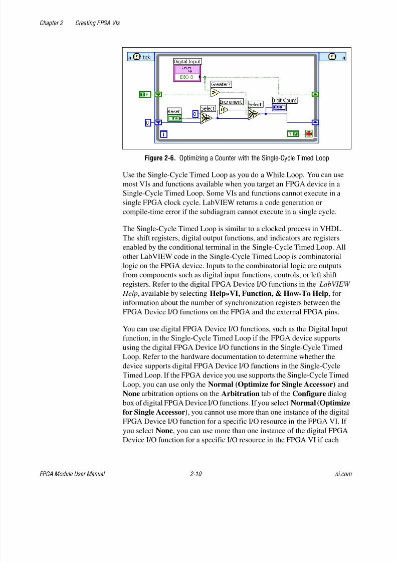
Use the Single-Cycle Timed Loop in an FPGA VI to execute code in oneclock cycle of the default FPGA clock. For example, you can optimize a
digital event counter application by using the Single-Cycle Timed Loop,
as shown in Figure 2-6.
8/13/2019 LabVIEW -FPGA Module User Manual
http://slidepdf.com/reader/full/labview-fpga-module-user-manual 25/62
8/13/2019 LabVIEW -FPGA Module User Manual
http://slidepdf.com/reader/full/labview-fpga-module-user-manual 26/62
Chapter 2 Creating FPGA VIs
© National Instruments Corporation 2-11 FPGA Module User Manual
instance is in a Single-Cycle Timed Loop. The default is Normal for the
Digital Output and Digital Port Output functions. You must manually
change the arbitration option in the Configure dialog box. Refer to
Chapter 3, Managing Shared Resources, for information about arbitration
and shared resources.
You can use the Flat Sequence or Stacked Sequence structure in the
Single-Cycle Timed Loop. However, all sequence frames execute in one
clock cycle. You cannot use any loop structures in a Single-Cycle Timed
Loop, including For Loops, While Loops, and other Single-Cycle Timed
Loops.
You cannot use more than one instance of a non-reentrant or shared subVI
in a Single-Cycle Timed Loop. You can use reentrant VIs if all instances of
the reentrant VI in the FPGA VI occur in the Single-Cycle Timed Loop.
Refer to the SubVIs on the FPGA section of this chapter for more
information about reentrant VIs.
You cannot use the Wait on Occurrence function in a Single-Cycle Timed
Loop. However, you can use the Set Occurrence function. You then can use
the Wait on Occurrence function outside the Single-Cycle Timed Loop in a
While Loop or For Loop.
You can use some functions in the Single-Cycle Timed Loop that take one
clock cycle to execute, such as the Memory Read VI. Wire the outputs of
such functions directly to uninitialized shift registers because the output
data is not valid until the next iteration of the Single-Cycle Timed Loop.
Refer to the LabVIEW Help, available by selecting Help»VI, Function,
& How-To Help, for more information about the Single-Cycle Timed
Loop and the VIs and functions you can use in the Single-Cycle Timed
Loop. Refer to the Using the Timed Loop to Write Multirate Applications
in LabVIEW Application Note and the LabVIEW Help, available by
selecting Help»VI, Function, & How-To Help, for information about
using the Timed Loop when you target LabVIEW for Windows or an RT
target.
Customizing I/OThe FPGA Module includes functions for performing basic I/O. However,
you might have applications that require more advanced or custom I/O
functionality. Use the FPGA Device I/O functions as building blocks to
create customized I/O functionality such as triggering and counters.
8/13/2019 LabVIEW -FPGA Module User Manual
http://slidepdf.com/reader/full/labview-fpga-module-user-manual 27/62
Chapter 2 Creating FPGA VIs
FPGA Module User Manual 2-12 ni.com
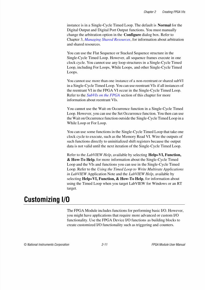
Creating TriggersIn many applications, you might need to wait for a trigger before
performing an action. You can wait for a trigger on a single digital input
using the Wait on Rising Edge method with the I/O Method Node.
Note The I/O resources available and the associated methods vary by execution target and
configuration. Refer to the hardware documentation in the LabVIEW Help, available by
selecting Help»VI, Function, & How-To Help, for information about available methods
and I/O resources.
The Wait on Rising Edge method waits until the specified condition is met
on the digital input before continuing. Place the I/O Method Node in the
first frame of a sequence structure and place the LabVIEW code for the task
in the following frame, as shown in Figure 2-7.
Figure 2-7. Creating a Trigger with the Wait on Rising Edge Method
You also can create more advanced triggering events from the FPGA
Device I/O functions. For example, you might need an application that
triggers only when multiple digital lines match a given condition, as shown
in Figure 2-8.
Figure 2-8. Triggering when Multiple Digital Lines Match a Condition
You can place the Digital Input function in a Single-Cycle Timed Loop and
exit the Single-Cycle Timed Loop only when the digital inputs match the
8/13/2019 LabVIEW -FPGA Module User Manual
http://slidepdf.com/reader/full/labview-fpga-module-user-manual 28/62
Chapter 2 Creating FPGA VIs
© National Instruments Corporation 2-13 FPGA Module User Manual
trigger pattern. Place the Single-Cycle Timed Loop in the first frame of a
sequence structure, just as you did for the Wait on Rising Edge method in
the previous example.
You can implement analog triggers using a While Loop in the same manner.
Place an Analog Input function and a Comparison function in a While Loopto trigger when the analog input value exceeds a programmable threshold.
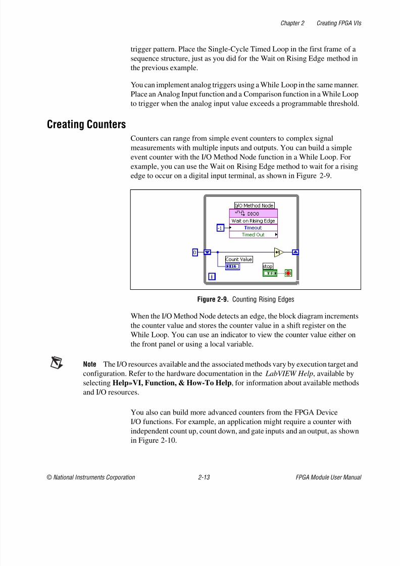
Creating CountersCounters can range from simple event counters to complex signal
measurements with multiple inputs and outputs. You can build a simple
event counter with the I/O Method Node function in a While Loop. For
example, you can use the Wait on Rising Edge method to wait for a rising
edge to occur on a digital input terminal, as shown in Figure 2-9.
Figure 2-9. Counting Rising Edges
When the I/O Method Node detects an edge, the block diagram increments
the counter value and stores the counter value in a shift register on the
While Loop. You can use an indicator to view the counter value either on
the front panel or using a local variable.
Note The I/O resources available and the associated methods vary by execution target and
configuration. Refer to the hardware documentation in the LabVIEW Help, available by
selecting Help»VI, Function, & How-To Help, for information about available methods
and I/O resources.
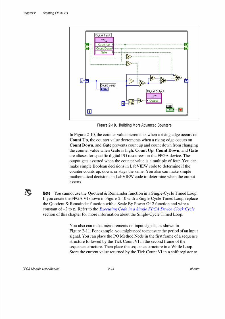
You also can build more advanced counters from the FPGA Device
I/O functions. For example, an application might require a counter with
independent count up, count down, and gate inputs and an output, as shown
in Figure 2-10.
8/13/2019 LabVIEW -FPGA Module User Manual
http://slidepdf.com/reader/full/labview-fpga-module-user-manual 29/62

8/13/2019 LabVIEW -FPGA Module User Manual
http://slidepdf.com/reader/full/labview-fpga-module-user-manual 30/62
Chapter 2 Creating FPGA VIs
© National Instruments Corporation 2-15 FPGA Module User Manual
create the previous value for the next iteration of the While Loop. Then
subtract the previous time from the current time to determine the period of
the input signal.
Figure 2-11. Measuring the Period of an Input Signal
Tip Use the Single-Cycle Timed Loop to increase execution speed and to decrease FPGA
usage and jitter in counter applications. Refer to the Executing Code in a Single FPGA
Device Clock Cycle section of this chapter for information about the Single-Cycle Timed
Loop.
Using Parallel Operations
As a fundamental part of the LabVIEW environment, LabVIEW allows
you to create VIs that include parallel operations. When the VI executes on
a processor-based target such as Windows, LabVIEW imitates parallel
operation by serially executing portions of the block diagram. In FPGA
VIs, parallel operations execute simultaneously on the FPGA device
because the FPGA Module creates dedicated hardware for each
independent VI or function in the FPGA VI.
Parallel Operations on the FPGAParallel operations on the FPGA typically increase determinism and
execution rate when compared to a processor-based target. Because the
parallel operations no longer contend over a common resource, such as
the processor LabVIEW for Windows uses, you increase determinism.
Because the overall execution time of multiple operations, with dedicated
hardware for each operation, is the execution time of the slowest operation,
8/13/2019 LabVIEW -FPGA Module User Manual
http://slidepdf.com/reader/full/labview-fpga-module-user-manual 31/62
Chapter 2 Creating FPGA VIs
FPGA Module User Manual 2-16 ni.com
you increase execution rate. With a single hardware resource, the overall
execution time for multiple operations is the sum of the execution times.
To create parallel operations, use multiple independent While Loops on
a single block diagram. For example, you can implement multiple data
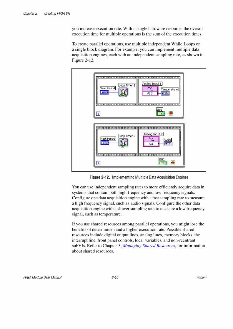
acquisition engines, each with an independent sampling rate, as shown inFigure 2-12.
Figure 2-12. Implementing Multiple Data Acquisition Engines
You can use independent sampling rates to more efficiently acquire data in
systems that contain both high frequency and low frequency signals.
Configure one data acquisition engine with a fast sampling rate to measure
a high frequency signal, such as audio signals. Configure the other data
acquisition engine with a slower sampling rate to measure a low frequency
signal, such as temperature.
If you use shared resources among parallel operations, you might lose the
benefits of determinism and a higher execution rate. Possible shared
resources include digital output lines, analog lines, memory blocks, the
interrupt line, front panel controls, local variables, and non-reentrant
subVIs. Refer to Chapter 3, Managing Shared Resources, for information
about shared resources.
8/13/2019 LabVIEW -FPGA Module User Manual
http://slidepdf.com/reader/full/labview-fpga-module-user-manual 32/62
Chapter 2 Creating FPGA VIs
© National Instruments Corporation 2-17 FPGA Module User Manual
Tip Each parallel operation uses a certain amount of space on the FPGA. If you begin to
run out of space on the FPGA and have identical parallel operations, you might save space
by creating a subVI for the operation and making it non-reentrant. However, you lose
parallel execution by creating a non-reentrant subVI for the operation.
SubVIs on the FPGALabVIEW allows you to encapsulate common sections of code as subVIs
to facilitate their reuse on the block diagram. You can configure the subVI
as a single instance shared among multiple callers, also known as a
non-reentrant VI. You also can configure the subVI to replicate itself for
each caller, also known as a reentrant VI. By default, LabVIEW subVIs are
non-reentrant VIs. To change the subVI to reentrant in the subVI, select
Execution from the Category pull-down menu of the VI Properties
dialog box and place a checkmark in the Reentrant Execution checkbox.
If you use a non-reentrant subVI in an FPGA VI, only a single copy of thesubVI becomes hardware and all callers share the hardware resource. If you
use a reentrant subVI in an FPGA VI, each call of the subVI generates a
dedicated hardware resource. For example, if you have five instances of an
event counter configured as a reentrant subVI on the block diagram,
LabVIEW implements five independent copies of the event counter
hardware on the FPGA.
Be careful not to use shared resources in reentrant subVIs when you want
to have dedicated hardware for each copy of the subVI. If you use any
shared resource in a reentrant subVI, only one copy of the shared resource
exists in hardware. Each reentrant subVI must use arbitration to access theshared resource. Refer to Chapter 3, Managing Shared Resources, for
information about shared resources.
Although non-reentrant subVIs typically consume less space in the FPGA
VI, the FPGA VI might run slower because it shares resources on the
FPGA. Reentrant VIs typically consume more space in the FPGA VI,
but the FPGA VI might run faster without shared resources. Table 2-1
summarizes the typical advantages and disadvantages of non-reentrant and
reentrant subVIs.
8/13/2019 LabVIEW -FPGA Module User Manual
http://slidepdf.com/reader/full/labview-fpga-module-user-manual 33/62
Chapter 2 Creating FPGA VIs
FPGA Module User Manual 2-18 ni.com
Transferring Data Among Parallel LoopsUse the FIFO Read and FIFO Write functions to transfer data to and from
loops, such as Single-Cycle Timed Loops, or from one subVI to another in
an FPGA VI. An FPGA FIFO acts like a fixed-length queue, where the first
value in is the first value out. Use the FIFO Write function to put data in an
FPGA FIFO. Use the FIFO Read function to retrieve the data from anotherloop or subVI.
FPGA FIFOs and LabVIEW queues both transfer data from one location to
another. However, unlike a LabVIEW queue, an FPGA FIFO imposes a
size restriction. You must configure the name, data type, and number of the
FPGA FIFO element when you place an FPGA FIFO function on the block
diagram. Both the reader and the writer can access the data in an FPGA
FIFO at the same time, allowing FPGA FIFOs to work properly in an
FPGAVI.
LabVIEW arbitrates different accessors to the same FIFO. Each FIFO has
separate arbitration for read access and write access. Right-click the FIFO
Read or FIFO Write function and select Arbitration options from the
shortcut menu to select an arbitration option. You can select Normal,
Optimize for Single, or None. LabVIEW globally applies the arbitration
option you select to all other accessors of the same FIFO. You must select
Optimize for Single if you use the FIFO Read or FIFO Write function in a
Single-Cycle Timed Loop. Refer to the Executing Code in a Single FPGA
Device Clock Cycle section of this chapter for information about using
Single-Cycle Timed Loops. Refer to Chapter 3, Managing Shared
Resources, for information about arbitration.
LabVIEW preserves the existing data when the FPGA FIFO is full. Rather
than overwriting the oldest element, the FIFO Write function returns TRUE
in the Full output to indicate the FPGA FIFO is full and no new data is
being stored in the FIFO. Refer to the LabVIEW Help, available by
Table 2-1. Non-Reentrant versus Reentrant SubVIs
VI Type FPGA Speed FPGA Utilization
Non-reentrant Slower—Each call to the subVI
waits until the previous call ends.
Lower—Only one instance of the subVI
exists on the FPGA no matter how many
times you use it.
Reentrant Faster—Multiple calls to the same
subVI run in parallel.
Higher—Each instance of the subVI on the
block diagram uses space on the FPGA.
8/13/2019 LabVIEW -FPGA Module User Manual
http://slidepdf.com/reader/full/labview-fpga-module-user-manual 34/62
8/13/2019 LabVIEW -FPGA Module User Manual
http://slidepdf.com/reader/full/labview-fpga-module-user-manual 35/62
Chapter 2 Creating FPGA VIs
FPGA Module User Manual 2-20 ni.com
range of the output data type. For example, the range of a U8 integer is 0
to 255. Adding two U8 integers together that have a result greater than 255
results in overflow, such as 200 + 70. When overflow occurs, the result rolls
over, or wraps, at the limit of the range and the result modulo 256 is
returned. For example, a result of 270 for a U8 integer wraps at 256 and
returns 14.
You can take advantage of the rollover behavior that occurs with overflow
in some applications. For example, the execution time measurement in
Figure 2-5 relies on the rollover behavior of overflow for proper operation.
The example shown in Figure 2-5 configures the Tick Count VIs with an
8-bit Size of Internal Counter and milliseconds for Counter Units. When
the internal counter of the Tick Count VI reaches 255 ms, it rolls over to 0.
If the first Tick Count VI returns a Tick Count of 132 ms and the execution
time of the LabVIEW code to be measured takes 140 ms, the internal
counter has rolled over and the second Tick Count VI returns a Tick Count
value of 16 ms. When the block diagram subtracts 132 from 16, overflowoccurs and results in the value of 140.
Note The Tick Count VI takes a single cycle to execute. In this example, if you set
Counter Units as Ticks instead of mSec, the returned result from the subtraction is 141
even though the LabVIEW code in the middle sequence takes only 140 ticks to execute.
If you want to avoid integer overflow, you can use the Scale By Power Of 2
function to reduce the magnitude of the inputs, use a larger output data type,
or use Saturation Arithmetic VIs. If you use the Scale By Power Of 2
function, you minimize the amount of space you use on the FPGA deviceto handle saturation. However, you lose precision and you also must
carefully program the FPGA VI to be sure you scale all inputs and outputs
correctly. If you use a larger output data type, you take up more space on
the FPGA device but you can program the FPGA VI more quickly and
easily and receive more accurate data. You can use the Saturation
Arithmetic VIs instead of other Numeric functions and select a larger
output type with the original input types, often resulting in more efficient
code in the FPGA VI.
Tip Use the smallest data type possible in FPGA VIs to minimize the space you use onthe FPGA.
If you want to allow overflow, you can use the Saturation Arithmetic VIs to
handle overflow if it occurs. You can saturate or wrap the result and show
the overflow terminal in the Configure dialog box of each Saturation
Arithmetic VI. Choose the Saturate option to minimize error if overflow
8/13/2019 LabVIEW -FPGA Module User Manual
http://slidepdf.com/reader/full/labview-fpga-module-user-manual 36/62
Chapter 2 Creating FPGA VIs
© National Instruments Corporation 2-21 FPGA Module User Manual
occurs and to avoid discontinuities in the signal. Choose the Wrap option
to use the smallest amount of space on the FPGA device. You also can use
the Numeric functions to implement the wrapping overflow mode.
Tip To save space on the FPGA, use the Wrap option in Saturation Arithmetic VIs when
possible. You then can use the overflow parameter to indicate when a particular result hasoverflowed.
You can configure the Saturation Arithmetic VIs to handle signed or
unsigned integer overflow. You also can configure the Saturation
Arithmetic VIs to return a maximum or minimum value if an overflow
condition occurs instead of performing modular arithmetic. Refer to the
LabVIEW Help, available by selecting Help»VI, Function, & How-To
Help, for more information about the Saturation Arithmetic VIs.
ArraysYou can use only fixed-size, one-dimensional arrays in FPGA VIs.
You can make any array constant, control, or indicator fixed-size by
right-clicking the array index and selecting Set Dimension Size from
the shortcut menu.
You cannot use an array function that returns a variable-size array.
However, if you use appropriate constants with many array functions,
the resulting array is fixed-size. For example, if you use the Array Subset
function, you must wire constants to the index and length parameters so
that the resulting subarray is fixed-size.
Tip Arrays consume significant amounts of space on the FPGA. To optimize compile
time, avoid using arrays larger than 32 elements.
MemoryYou can use FPGA memory for data storage in the FPGA VI. You access
the FPGA memory using the Memory Read and Memory Write VIs
available with the FPGA Module. You can use these VIs to perform basic
read and write operations to the FPGA memory and as building blocks to
create more advanced memory functions such as FIFOs, dual-portedmemory, look-up tables, and so on.
You can create look-up tables with constant or variable entries in FPGA
VIs. You can use fixed-size arrays for smaller look-up tables with variable
entries. You can use constant fixed-size arrays when the look-up table
entries do not need to change and you want to limit FPGA usage. For larger
8/13/2019 LabVIEW -FPGA Module User Manual
http://slidepdf.com/reader/full/labview-fpga-module-user-manual 37/62
Chapter 2 Creating FPGA VIs
FPGA Module User Manual 2-22 ni.com
look-up tables, use the Look-Up Table 1D VI available with the FPGA
Module to create look-up tables with variable entries in the FPGA memory.
Using HDL Code in FPGA VIsYou can use the LabVIEW FPGA Module to rapidly prototype and develop
hardware in the same intuitive programming environment you use to
develop software applications. However, you might have algorithms or
applications in a text-based hardware description language (HDL) that you
want to use in FPGA VIs without rewriting the code in LabVIEW. If you
have a block of HDL code you want to use in an FPGA VI, you can enter
the code in the HDL Interface Node rather than rewriting the code in
LabVIEW. You enter all the parameters and the HDL code in the
Configure HDL Interface Node dialog box. You then wire the parameters
you entered as you do any VI or function on the block diagram. Do not
use the HDL Interface Node if are not already familiar with an HDL
programming language. Refer to the NI Developer Zone at ni.com/zone and enter the info code exkta6 for more information about using HDL
code in FPGA VIs.
Controlling I/O Power-On States
An application might require that the I/O on the FPGA device be set to a
known value when the system powers on. For example, if an FPGA device
controls hydraulic valves with the digital outputs, the FPGA device must
keep the valves turned off until the host VI is launched and starts to control
the system. You can create an FPGA VI and configure the FPGA device toset the power-on states of the FPGA device.
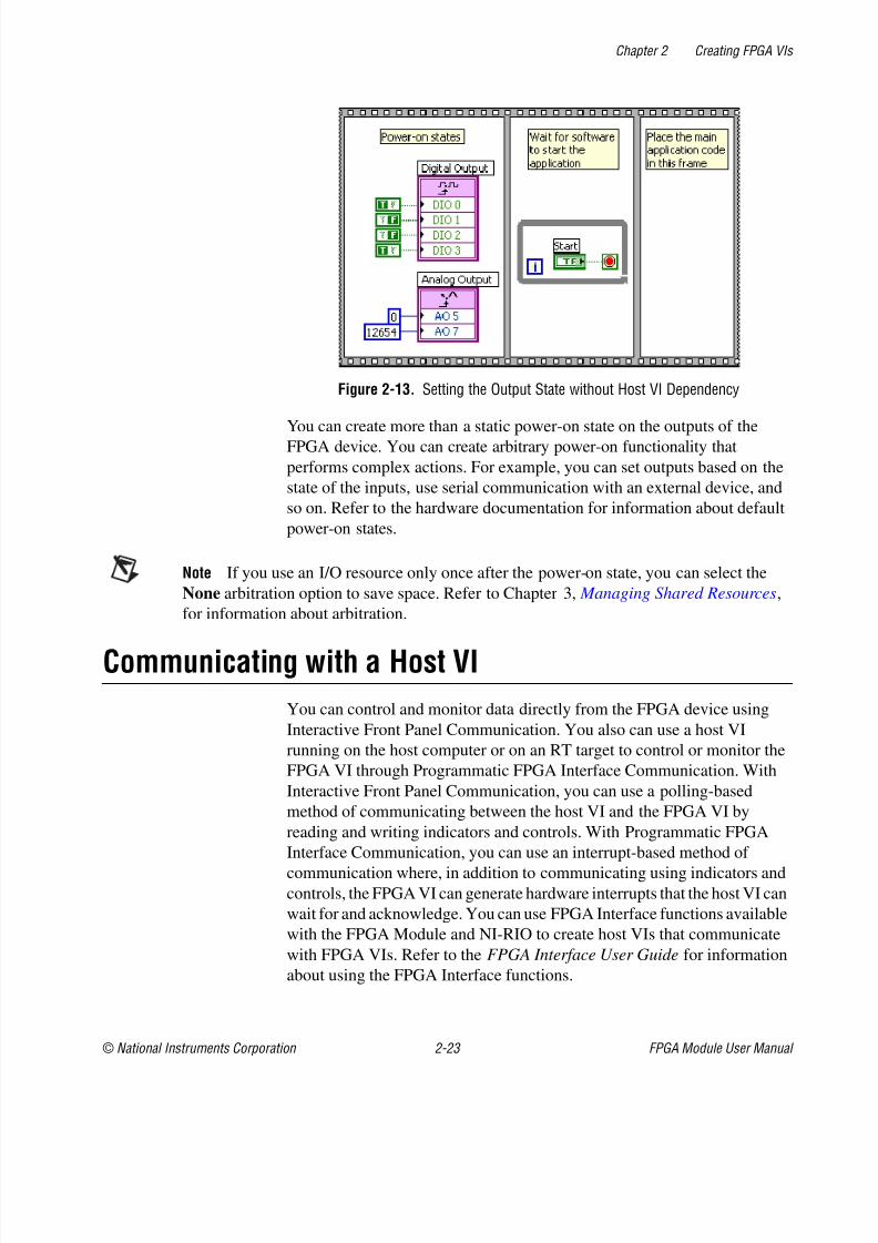
You must program the FPGA VI so that the block diagram sets the output
states without any dependencies on the host VI. For example, you can place
the digital and analog output functions in the first frame of a sequence
structure. You then place the rest of the LabVIEW code in the subsequent
frames of the sequence structure, as shown in Figure 2-13. Then configure
the FPGA VI to start executing as soon as it is loaded in the FPGA. Compile
and download the FPGA VI to the flash memory on the FPGA device and
configure the FPGA device to automatically load the FPGA VI from theflash memory when the FPGA device powers on. When the FPGA device
powers on, the FPGA VI loads into the FPGA from the flash memory, and
the FPGA VI starts executing immediately. The output functions in the first
frame of the sequence structure on the FPGA VI set the output states. Refer
to Chapter 4, Running FPGA VIs, for information about automatically
loading and running FPGA VIs.
8/13/2019 LabVIEW -FPGA Module User Manual
http://slidepdf.com/reader/full/labview-fpga-module-user-manual 38/62
Chapter 2 Creating FPGA VIs
© National Instruments Corporation 2-23 FPGA Module User Manual
Figure 2-13. Setting the Output State without Host VI Dependency
You can create more than a static power-on state on the outputs of theFPGA device. You can create arbitrary power-on functionality that
performs complex actions. For example, you can set outputs based on the
state of the inputs, use serial communication with an external device, and
so on. Refer to the hardware documentation for information about default
power-on states.
Note If you use an I/O resource only once after the power-on state, you can select the
None arbitration option to save space. Refer to Chapter 3, Managing Shared Resources,
for information about arbitration.
Communicating with a Host VI
You can control and monitor data directly from the FPGA device using
Interactive Front Panel Communication. You also can use a host VI
running on the host computer or on an RT target to control or monitor the
FPGA VI through Programmatic FPGA Interface Communication. With
Interactive Front Panel Communication, you can use a polling-based
method of communicating between the host VI and the FPGA VI by
reading and writing indicators and controls. With Programmatic FPGA
Interface Communication, you can use an interrupt-based method ofcommunication where, in addition to communicating using indicators and
controls, the FPGA VI can generate hardware interrupts that the host VI can
wait for and acknowledge. You can use FPGA Interface functions available
with the FPGA Module and NI-RIO to create host VIs that communicate
with FPGA VIs. Refer to the FPGA Interface User Guide for information
about using the FPGA Interface functions.
8/13/2019 LabVIEW -FPGA Module User Manual
http://slidepdf.com/reader/full/labview-fpga-module-user-manual 39/62
Chapter 2 Creating FPGA VIs
FPGA Module User Manual 2-24 ni.com
A host VI can control and monitor only data passed through the FPGA VI
front panel. For example, if you want the host VI to monitor the data from
an analog input terminal, you must wire an indicator to the Analog Input
function on the FPGA VI block diagram.
Interrupt-Based CommunicationYou can use interrupts to notify the host VI of events, such as data being
ready, an error occurring, or a task finishing. An interrupt is a physical
hardware line to the host that the FPGA device asserts.
Use the Interrupt VI in FPGA VIs to generate any of the 32 independent
logical interrupts available on the FPGA device. Each logical interrupt
specifies the reason for causing the interrupt and allows you to handle it
differently in software. You can set the Interrupt VI to wait until the host VI
acknowledges the interrupt on the FPGA device by wiring the Wait Until
Cleared input. In this case, the Interrupt VI waits until the host VIcontrolling the device acknowledges the interrupt. Refer to the LabVIEW
Help, available by selecting Help»VI, Function, & How-To Help, for
more information about the Interrupt VI.
Use caution when you include simultaneous interrupt calls on the FPGA
device. The interrupt becomes a shared resource if you use more than one,
and this can induce jitter. Refer to Chapter 3, Managing Shared Resources,
for more information about resolving resource contention.
The advantage of using interrupt-based communication instead of
polling-based communication is that the host VI can perform otheroperations while waiting for the interrupt. In contrast, if the host VI uses
polling-based communication, the host VI does not have time to perform
other operations while waiting for a specific data value from the FPGA
device.
8/13/2019 LabVIEW -FPGA Module User Manual
http://slidepdf.com/reader/full/labview-fpga-module-user-manual 40/62
© National Instruments Corporation 3-1 FPGA Module User Manual
3Managing Shared Resources
This chapter describes how to use arbitration on shared resources in
FPGAVIs. If the FPGA VI design fits on the FPGA and if the FPGA VI
meets the performance expectations, keep the default Arbitration options.
Resource Contention and Arbitration
Many applications contain resources that are accessed from multiple
functions or VIs in an FPGA VI. For example, an application might use the
FPGA memory to temporarily store data from two independently operatingdata acquisition loops. The FPGA Module includes arbitration to determine
which location can access the resource if the locations request access at the
same time.
Resource contention occurs when you include two or more functions or VIs
on the FPGA VI block diagram that simultaneously request access to the
same shared resource. A requestor becomes an accessor when it actively
requests information from a specific resource and is granted access by a
special component called an arbiter . The arbiter determines which
requestor becomes an accessor when resource contention occurs. Possible
shared resources include digital output lines, analog lines, memory blocks,
the interrupt line, front panel controls, local variables, and non-reentrant
subVIs.
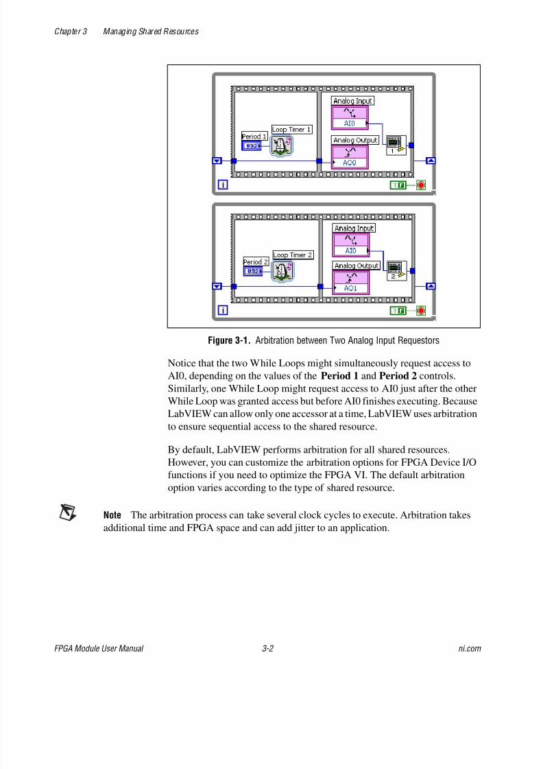
Figure 3-1 illustrates an FPGA VI with arbitration between the first and
second requestor of AI0.
8/13/2019 LabVIEW -FPGA Module User Manual
http://slidepdf.com/reader/full/labview-fpga-module-user-manual 41/62
8/13/2019 LabVIEW -FPGA Module User Manual
http://slidepdf.com/reader/full/labview-fpga-module-user-manual 42/62
Chapter 3 Managing Shared Resources
© National Instruments Corporation 3-3 FPGA Module User Manual
Jitter
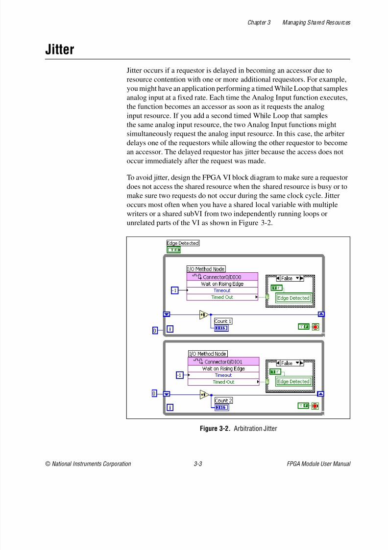
Jitter occurs if a requestor is delayed in becoming an accessor due to
resource contention with one or more additional requestors. For example,
you might have an application performing a timed While Loop that samples
analog input at a fixed rate. Each time the Analog Input function executes,
the function becomes an accessor as soon as it requests the analog
input resource. If you add a second timed While Loop that samples
the same analog input resource, the two Analog Input functions might
simultaneously request the analog input resource. In this case, the arbiter
delays one of the requestors while allowing the other requestor to become
an accessor. The delayed requestor has jitter because the access does not
occur immediately after the request was made.
To avoid jitter, design the FPGA VI block diagram to make sure a requestor
does not access the shared resource when the shared resource is busy or tomake sure two requests do not occur during the same clock cycle. Jitter
occurs most often when you have a shared local variable with multiple
writers or a shared subVI from two independently running loops or
unrelated parts of the VI as shown in Figure 3-2.
Figure 3-2. Arbitration Jitter
8/13/2019 LabVIEW -FPGA Module User Manual
http://slidepdf.com/reader/full/labview-fpga-module-user-manual 43/62
Chapter 3 Managing Shared Resources
FPGA Module User Manual 3-4 ni.com
The VI in Figure 3-2 shows two While Loops that might attempt to write to
the Edge Detected local variable simultaneously. The arbiter allows one
While Loop to access Edge Detected at a time. The other While Loop does
not access Edge Detected until after the first While Loop finishes. Jitter is
introduced into the delayed While Loop.
The possibility of jitter grows with the number of accessors. If you do not
schedule simultaneous requests, the delay through the arbiter is constant
regardless of the number of potential accessors.
Arbitration Options
The following arbitration options are available with the FPGA Module:
• Normal
• Normal (Optimize for Single Accessor)
• None
An arbiter performs the following general steps during arbitration.
1. Waits for one or more requestors. If multiple requestors request access,
the arbiter determines which requestor becomes the accessor.
2. Passes data from the accessor to the resource.
3. Begins resource execution.
4. Waits for the resource to complete execution.
5. Passes data back to the accessor.6. Prepares the resource for another execution.
7. Waits for the next requestor.
NormalA resource with the Normal arbitration option always uses an arbiter, even
if only one requestor requests access. The Normal arbiter is a fair round
robin arbiter that ensures sequential access to a shared resource. The arbiter
does not allow a requestor to become an accessor again until all other
waiting requestors have become accessors. Consequently, jitter occurs ifyou have more than one simultaneous requestor. Refer to the Jitter section
of this chapter for more information.
8/13/2019 LabVIEW -FPGA Module User Manual
http://slidepdf.com/reader/full/labview-fpga-module-user-manual 44/62
Chapter 3 Managing Shared Resources
© National Instruments Corporation 3-5 FPGA Module User Manual
Normal (Optimize for Single Accessor)A resource with the Normal (Optimize for Single Accessor) option does
not use an arbiter if the FPGA VI contains only one requestor. If the FPGA
VI has multiple requestors, LabVIEW uses Normal arbitration even if the
requests are not simultaneous. You can save time and space in FPGA VIs if
you use the Normal (Optimize for Single Accessor) arbitration option if
the FPGA VI contains only one requestor.
Use the Normal (Optimize for Single Accessor) option in the following
situations:
• You have a large FPGA VI and need to save space.
• You have only one accessor for a resource.
• You do not need single requestor channels synchronized with multiple
requestor channels. Refer to the Timing section of this chapter for
information about synchronized channels.
NoneA resource with the None option does not arbitrate simultaneous requests,
which saves significant space on the FPGA. To use the None option, you
must guarantee sequential access to the resource in the data flow of the
FPGA VI. If you attempt to make simultaneous requests in the FPGA VI,
you make simultaneous accesses and corrupt data.
Available Arbitration Options for Specific ResourcesYou can select arbitration options for most FPGA device I/O resources, as
shown in Table 3-1. D is the default option, and O indicates other available
options.
Note Available arbitration options vary by execution target. Refer to the hardware
documentation in the LabVIEW Help, available by selecting Help»VI, Function,
& How-To Help, for information about available arbitration options.
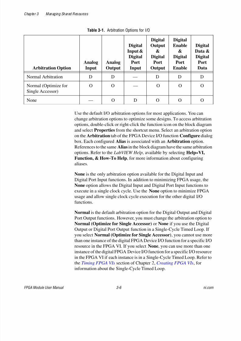
8/13/2019 LabVIEW -FPGA Module User Manual
http://slidepdf.com/reader/full/labview-fpga-module-user-manual 45/62
Chapter 3 Managing Shared Resources
FPGA Module User Manual 3-6 ni.com
Use the default I/O arbitration options for most applications. You can
change arbitration options to optimize some designs. To access arbitrationoptions, double-click or right-click the function icon on the block diagram
and select Properties from the shortcut menu. Select an arbitration option
on the Arbitration tab of the FPGA Device I/O function Configure dialog
box. Each configured Alias is associated with an Arbitration option.
References to the same Alias in the block diagram have the same arbitration
options. Refer to the LabVIEW Help, available by selecting Help»VI,
Function, & How-To Help, for more information about configuring
aliases.
None is the only arbitration option available for the Digital Input andDigital Port Input functions. In addition to minimizing FPGA usage, the
None option allows the Digital Input and Digital Port Input functions to
execute in a single clock cycle. Use the None option to minimize FPGA
usage and allow single clock cycle execution for the other digital I/O
functions.
Normal is the default arbitration option for the Digital Output and Digital
Port Output functions. However, you must change the arbitration option to
Normal (Optimize for Single Accessor) or None if you use the Digital
Output or Digital Port Output function in a Single-Cycle Timed Loop. If
you select Normal (Optimize for Single Accessor), you cannot use morethan one instance of the digital FPGA Device I/O function for a specific I/O
resource in the FPGA VI. If you select None, you can use more than one
instance of the digital FPGA Device I/O function for a specific I/O resource
in the FPGA VI if each instance is in a Single-Cycle Timed Loop. Refer to
the Timing FPGA VIs section of Chapter 2, Creating FPGA VIs, for
information about the Single-Cycle Timed Loop.
Table 3-1. Arbitration Options for I/O
Arbitration Option
Analog
Input
Analog
Output
Digital
Input &
DigitalPort
Input
Digital
Output
&
DigitalPort
Output
Digital
Enable
&
DigitalPort
Enable
Digital
Data &
DigitalPort
Data
Normal Arbitration D D — D D D
Normal (Optimize for
Single Accessor)
O O — O O O
None — O D O O O
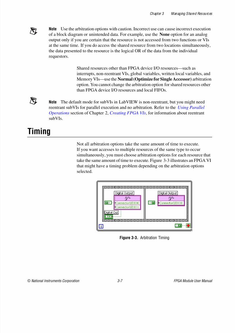
8/13/2019 LabVIEW -FPGA Module User Manual
http://slidepdf.com/reader/full/labview-fpga-module-user-manual 46/62
8/13/2019 LabVIEW -FPGA Module User Manual
http://slidepdf.com/reader/full/labview-fpga-module-user-manual 47/62
Chapter 3 Managing Shared Resources
FPGA Module User Manual 3-8 ni.com
The Digital Output functions shown in Figure 3-3 have three arbitration
options. If you choose the Normal arbitration option, LabVIEW
implements an equivalent arbiter for both Connector0/DIO0 and
Connector0/DIO1. Both arbiters take the same amount of time to execute,
so Connector0/DIO0 and Connector0/DIO1 output simultaneously in the
first frame of the Flat Sequence structure.
If you choose the Normal (Optimize for Single Accessor) arbitration
option, LabVIEW implements a different arbiter for each of
Connector0/DIO0 and Connector0/DIO1. Connector0/DIO0 uses a normal
arbiter because the block diagram requests access to Connector0/DIO0
twice. Connector0/DIO1 uses no arbiter because the block diagram
requests access to Connector0/DIO1 only once. Connector0/DIO0 takes
longer to execute than Connector0/DIO1, so Connector0/DIO0 and
Connector0/DIO1 do not output simultaneously in the first frame of the Flat
Sequence structure.
If you choose the None arbitration option for both Digital Output functions,
LabVIEW does not implement an arbiter for either Connector0/DIO0 or
Connector0/DIO1. Therefore, Connector0/DIO0 and Connector0/DIO1
output simultaneously.
FPGA Utilization
Arbitration also can use a significant amount of space on the FPGA. If you
can decrease the number of requestors of a resource to one, use the Normal
(Optimize for Single Accessor) arbitration option. The single requestorrequires no arbitration. If you have two requestors, LabVIEW uses Normal
arbitration, even if Normal (Optimize for Single Accessor) is selected.
8/13/2019 LabVIEW -FPGA Module User Manual
http://slidepdf.com/reader/full/labview-fpga-module-user-manual 48/62
8/13/2019 LabVIEW -FPGA Module User Manual
http://slidepdf.com/reader/full/labview-fpga-module-user-manual 49/62
Chapter 4 Running FPGA VIs
FPGA Module User Manual 4-2 ni.com
You can test an FPGA VI before compiling it. Refer to Chapter 5,
Debugging FPGA VIs, for information about testing FPGA VIs using
emulators.
Compiling FPGA VIs Using the LabVIEW FPGA Compile ServerLabVIEW and the LabVIEW FPGA Compile Server have a client-server
architecture, where LabVIEW is a client to the LabVIEW FPGA Compile
Server. The client-server architecture allows you to disconnect LabVIEW
from the LabVIEW FPGA Compile Server during a compile. You then can
continue to use LabVIEW while the FPGA VI compiles. You must not
modify the FPGA VI being compiled. To reconnect, you again run the
FPGA VI targeted to the FPGA device. LabVIEW displays a compile
report when the compile is complete. You can view the compile report if
you are connected to the LabVIEW FPGA Compile Server. After you click
the OK button in the Successful Compile Report window, LabVIEW
embeds the new bitstream into the FPGA VI and downloads the bitstreamto the FPGA. The FPGA VI then runs on the FPGA device and you can
interact with it through the front panel on the development computer using
Interactive Front Panel Communication.
The LabVIEW FPGA Compile Server launches automatically when you
run an FPGA VI that is not compiled or that you modified since the last
compile. LabVIEW converts the VI into intermediate files to send to the
LabVIEW FPGA Compile Server. The LabVIEW FPGA Compile Server
converts the intermediate files into a bitstream.
The compile time depends on the size of the VI, the processor speed, andamount of memory in the computer on which you are compiling. National
Instruments recommends at least 512 MB of memory for the LabVIEW
FPGA Compile Server. If you have less memory, smaller block diagrams
might compile quickly, but larger block diagrams might use large amounts
of virtual memory, which can be very slow, and compiles can take over 10
times longer to complete.
The LabVIEW FPGA Compile Server does not close automatically.
You can close it by clicking the Stop Server button.
Compiling on a Remote ComputerYou can install the LabVIEW FPGA Compile Server on a remote
computer. You might want to do this if the development computer is slow
and does not have enough memory to compile for the FPGA device.
By default, LabVIEW assumes the LabVIEW FPGA Compile Server is
installed on the local computer. To select a remote LabVIEW FPGA
8/13/2019 LabVIEW -FPGA Module User Manual
http://slidepdf.com/reader/full/labview-fpga-module-user-manual 50/62
Chapter 4 Running FPGA VIs
© National Instruments Corporation 4-3 FPGA Module User Manual
Compile Server, select Target»Build Options in the Embedded Project
Manager window and enter the name or IP address and server port of the
remote computer running the LabVIEW FPGA Compile Server.
Depending on the network, you also might need to increase the network
timeout.
Launch the LabVIEW FPGA Compile Server manually on the remote
computer by selecting Start»Programs»National Instruments»
LabVIEW»LabVIEW FPGA Utilities»CompileServer. You must
launch the LabVIEW FPGA Compile Server manually when you configure
LabVIEW clients on other computers to connect to the remote computer for
compiling.
Managing Compilation FilesThe LabVIEW FPGA Compile Server stores all files it uses to compile a
VI in a directory. Configure the directory by clicking the Configure buttonin the LabVIEW FPGA Compile Server window. Click the Compile List
button to view the compile history and delete compile files you no longer
need. Typically, you do not need compile files after the bitstream is
embedded in the FPGA VI. Delete the contents of X :\NIFPGA11\
clntTmp and X :\NIFPGA11\srvrTmp, where X is the drive where you
installed LabVIEW and the FPGA Module, to save space on the hard drive.
Using Compiled FPGA VI Options
This section describes the clock rate and auto run options available with theFPGA Module to compile into FPGA VIs. Each type of FPGA device
might have specific options available. Refer to the LabVIEW Help,
available by selecting Help»VI, Function, & How-To Help, for more
information about device-specific options.
Changing the FPGA Device Clock RateThe FPGA device provides a 40 MHz clock to control the internal
operations on the FPGA. The internal clock determines the execution time
of the individual VIs and functions on the FPGA VI block diagram.
Most FPGA VIs can execute properly using this clock. You also can
compile FPGA VIs with faster clock rates for higher performance.
However, not all FPGA VIs can compile properly with faster clock rates.
If you select a clock rate that is too fast for the FPGA VI, the Error in
Compilation dialog box tells you the compile failed. You must select a
lower clock rate and try the compile again.
8/13/2019 LabVIEW -FPGA Module User Manual
http://slidepdf.com/reader/full/labview-fpga-module-user-manual 51/62
Chapter 4 Running FPGA VIs
FPGA Module User Manual 4-4 ni.com
Note If you increase the FPGA device clock rate, less code can execute in the
Single-Cycle Timed Loop because the clock cycle is shorter. Refer to the Timing FPGA
VIs section of Chapter 2, Creating FPGA VIs, for more information about the Single-Cycle
Timed Loop.
Change the global default clock rate for an FPGA device by selectingTarget»Build Options in the Embedded Project Manager window.
All subsequent FPGA VIs you create for that FPGA device have the new
default clock rate. You can change the clock rate for a top-level FPGA VI
by selecting Target»Build in the Embedded Project Manager window.
The LabVIEW FPGA Compile Server compiles the clock rate for the
specific FPGA VI into the bitstream. Each time you compile the same
FPGA VI, the FPGA VI retains the same clock rate.
Configuring FPGA VIs to Run Automatically
Some FPGA devices have flash memory that can store FPGA VIs.If you want a VI that is loaded to the FPGA from flash memory to run
automatically on an FPGA device, change the Default Auto Run option
for the FPGA device by selecting Target»Build Options in the Embedded
Project Manager window. All subsequent FPGA VIs you create for that
FPGA device have the new Default Auto Run setting. You can change the
Auto Run VI option for every instance of a specific FPGA VI by selecting
Target»Build in the Embedded Project Manager window. Refer to the
Running FPGA VIs at Power On section of this chapter for information
about storing the FPGA VI in flash memory.
Downloading Compiled FPGA VIs to the FPGA Device
When you click the Run button on a new or changed FPGA VI
while targeting an FPGA device, LabVIEW downloads the FPGA VI to the
FPGA automatically after the compile completes. LabVIEW automatically
downloads a previously compiled VI when you target an FPGA device and
click the Run button. LabVIEW does not download the FPGA VI if it is
already on the FPGA device. You can force a download by clicking the
Download button in the Embedded Project Manager window. You might
force a download if you want to reinitialize the FPGA to its default state.
When you target LabVIEW to Windows or an RT target, you can
programmatically download FPGA VIs to FPGA devices. Refer to
the FPGA Interface User Guide and the LabVIEW Help, available by
selecting Help»VI, Function, & How-To Help, for information about
programmatically downloading FPGA VIs.
8/13/2019 LabVIEW -FPGA Module User Manual
http://slidepdf.com/reader/full/labview-fpga-module-user-manual 52/62
8/13/2019 LabVIEW -FPGA Module User Manual
http://slidepdf.com/reader/full/labview-fpga-module-user-manual 53/62
Chapter 4 Running FPGA VIs
FPGA Module User Manual 4-6 ni.com
Setting Target Configurations
Some FPGA devices have configuration information stored in flash
memory. Select Tools»Download VI or Attributes to Flash Memory in
the Embedded Project Manager window to configure the flash memory
options.
For example, the NI PXI-7831R stores two configuration options in flash
memory—Sync to PXI Clock and Analog Signal Connection. The FPGA
clock source is internal by default, or you can synchronize the FPGA device
to the 10 MHz clock of a PXI chassis. Use this feature when you want
multiple FPGA devices to synchronize the FPGA device clocks to the same
PXI clock. Refer to the hardware documentation for more information
about the configuration options.
8/13/2019 LabVIEW -FPGA Module User Manual
http://slidepdf.com/reader/full/labview-fpga-module-user-manual 54/62
© National Instruments Corporation 5-1 FPGA Module User Manual
5Debugging FPGA VIs
This chapter describes debugging techniques you can use to test FPGA VIs.
You can use traditional LabVIEW debugging techniques only when you
target the FPGA VI to an emulator or run the FPGA VI on the host
computer. You cannot use traditional LabVIEW debugging techniques,
such as execution highlighting and probing, with LabVIEW targeted to an
FPGA device.
Refer to the LabVIEW User Manual for information about traditional
LabVIEW debugging techniques.
Testing a VI Before Compiling
You can test the logic of an FPGA VI before compiling it by targeting an
emulator. To target an emulator rather than the FPGA device, select the
execution target that matches the FPGA device. For example, if the device
appears in the Operate»Switch Execution Target menu as FPGA Device
(7831R), the emulator for that device appears in the same menu as FPGA
Emulator (7831R). You can use an emulator with any available FPGA
device.
When you run an FPGA VI with an emulator, LabVIEW downloads the
pre-compiled emulation VI included with the FPGA Module to the FPGA
device to provide I/O, and the FPGA VI runs on the host computer.
LabVIEW then communicates with the emulation VI on the FPGA while
both VIs run. The FPGA Module includes a pre-compiled emulation VI for
some FPGA device targets. Refer to the hardware documentation for
information about the availability of an emulator.
You can use all traditional LabVIEW debugging tools, such as probes,
execution highlighting, breakpoints, and single-stepping. You cannot test
certain behavior, such as timing and determinism, with an emulator because
the FPGA VI runs on the host computer instead of the FPGA. The emulator
tries to preserve the timing of the Loop Timer, Wait, and Tick Count VIs as
much as possible. The emulator does not preserve the timing of the
Single-Cycle Timed Loop. The code in a Single-Cycle Timed Loop
executes as quickly as possible on the host computer. Other VIs and
functions also execute as quickly as possible.
8/13/2019 LabVIEW -FPGA Module User Manual
http://slidepdf.com/reader/full/labview-fpga-module-user-manual 55/62
Chapter 5 Debugging FPGA VIs
FPGA Module User Manual 5-2 ni.com
Note You must have an FPGA device installed to use an emulator. However, you still
can debug the FPGA VI without an FPGA device by targeting LabVIEW for Windows.
When you run an FPGA VI while targeting LabVIEW for Windows, LabVIEW generates
random data for the FPGA Device I/O functions.
Building Debugging into an FPGA VIIn addition to using emulators, you can build debugging functionality into
the FPGA VI with additional indicators or additional I/O. You can use
additional indicators and additional I/O with Interactive Front Panel
Communication or Programmatic FPGA Interface Communication.
Adding IndicatorsYou can add indicators to the FPGA VI block diagram to monitor the
internal state of the FPGA VI. Use indicators as you do probes. Place anindicator anywhere on the block diagram where you need to see data to
verify the functionality of the VI. You also can perform more advanced
debugging by using controls to change execution of the FPGA VI.
If you use additional indicators with Programmatic FPGA Interface
Communication, you must program the host VI to read the additional
indicators.
Note Adding indicators to the FPGA VI takes up more space on the FPGA. Be sure to
remove debugging indicators if you encounter space constraints on the FPGA.
An indicator consumes a small amount of execution time, which can affect
the performance of the FPGA VI. Whenever possible, add debugging
indicators in parallel to other operations in the FPGA VI to minimize the
effect on execution time.
Adding I/OIf you have unused I/O resources on the FPGA device, you can add
additional I/O terminals to the FPGA VI block diagram to aid debugging.
You can easily monitor the internal state of Boolean logic, triggers, and soon. You can create more advanced debugging tools by adding LabVIEW
code to analyze data and events and to control flow.
8/13/2019 LabVIEW -FPGA Module User Manual
http://slidepdf.com/reader/full/labview-fpga-module-user-manual 56/62
© National Instruments Corporation A-1 FPGA Module User Manual
ATechnical Support and
Professional Services
Visit the following sections of the National Instruments Web site at
ni.com for technical support and professional services:
• Support—Online technical support resources at ni.com/support
include the following:
– Self-Help Resources—For immediate answers and solutions,
visit the award-winning National Instruments Web site for
software drivers and updates, a searchable KnowledgeBase,product manuals, step-by-step troubleshooting wizards, thousands
of example programs, tutorials, application notes, instrument
drivers, and so on.
– Free Technical Support—All registered users receive free Basic
Service, which includes access to hundreds of Application
Engineers worldwide in the NI Developer Exchange at
ni.com/exchange. National Instruments Application Engineers
make sure every question receives an answer.
• Training and Certification—Visit ni.com/training for
self-paced training, eLearning virtual classrooms, interactive CDs,and Certification program information. You also can register for
instructor-led, hands-on courses at locations around the world.
• System Integration—If you have time constraints, limited in-house
technical resources, or other project challenges, NI Alliance Program
members can help. To learn more, call your local NI office or visit
ni.com/alliance.
If you searched ni.com and could not find the answers you need, contact
your local office or NI corporate headquarters. Phone numbers for our
worldwide offices are listed at the front of this manual. You also can visitthe Worldwide Offices section of ni.com/niglobal to access the branch
office Web sites, which provide up-to-date contact information, support
phone numbers, email addresses, and current events.
8/13/2019 LabVIEW -FPGA Module User Manual
http://slidepdf.com/reader/full/labview-fpga-module-user-manual 57/62
© National Instruments Corporation G-1 FPGA Module User Manual
Glossary
Symbol Prefix Value
p pico 10–12
n nano 10–9
µ micro 10– 6
m milli 10–3
k kilo 103
M mega 106
G giga 109
T tera 1012
A
accessor A hardware component that has been granted access to a specific shared
resource by an arbiter.
ADC Analog-to-digital converter—an electronic device, often an integrated
circuit, that converts an analog voltage to a digital number.
alias A user defined name for an I/O terminal, displayed on the FPGA Device
I/O function icon on the block diagram. For example, you can create an
alias for AI0 named Oven Temperature that appears in the Analog Input
function icon on the block diagram. The complete list of aliases created in
an LEP file appears in the Configure dialog box for each FPGA Device
I/O function in FPGA VIs in the LEP file as well as in the Alias Manager
dialog box. Aliases configured in one LEP file do not appear in other LEP
files.
arbiter A hardware component that controls access to a shared resource anddetermines which requestor becomes the accessor of the shared resource.
The arbiter resolves resource contention over the shared resource.
arbitration The process of resolving resource contention by determining which
requestor of a shared resource is granted access to the shared resource.
8/13/2019 LabVIEW -FPGA Module User Manual
http://slidepdf.com/reader/full/labview-fpga-module-user-manual 58/62
Glossary
FPGA Module User Manual G-2 ni.com
B
bitstream Programming information that is downloaded to an FPGA device to
determine its behavior.
C
compile for FPGA The process of creating a bitstream from an FPGA VI.
D
DAC Digital-to-analog converter—an electronic device, often an integrated
circuit, that converts a digital number into a corresponding analog voltage
or current.
default FPGA clock Clock input for all flip-flops in an FPGA VI. You can configure the default
value for a specific FPGA device in the FPGA Target Options dialog box.
You can configure the value for a specific FPGA VI in the FPGA Project
Builder dialog box.
determinism Characteristic of a system that describes how consistently it can respond to
external events or perform operations within a given time limit.
development computer The computer on which you develop LabVIEW VIs. The VIs can run on
different execution targets.
device An instrument or controller you can access as a single entity that controls
or monitors real-world I/O points. A device often is connected to a host
computer through some type of communication network.
E
emulation VI The VI that the emulator downloads to the FPGA device so you can test and
debug an FPGA VI without compiling and downloading the FPGA VI.
emulator A target you can select from the Switch Execution Target list that mimics
the behavior of an FPGA device. The emulator runs the FPGA VI on the
host computer and accesses the emulation VI running on the FPGA device
to provide real I/O. You can use the emulator to test and debug FPGA VIs
without compiling and downloading the FPGA VIs.
8/13/2019 LabVIEW -FPGA Module User Manual
http://slidepdf.com/reader/full/labview-fpga-module-user-manual 59/62
Glossary
© National Instruments Corporation G-3 FPGA Module User Manual
execution target The computer or device that runs a LabVIEW VI. An execution target can
be an FPGA device, an RT target, or the development computer.
F
FIFO First In First Out.
flash memory Non-volatile storage that retains its contents even when the device
powers off.
FPGA Field-Programmable Gate Array—programmable logic device (PLD) with
a high density of gates.
FPGA device A Reconfigurable I/O device that contains a reconfigurable FPGA
surrounded by fixed I/O resources.
FPGA DeviceI/O function
A type of function available when you target an FPGA device. Use theFPGA Device I/O functions to perform I/O operations on an FPGA device.
FPGA Interface
function
A type of function that enables communication between a host VI and an
FPGA VI. Available when you target LabVIEW for Windows or an RT
target. Refer to the FPGA Interface User Guide and the LabVIEW Help,
available by selecting Help»VI, Function, & How-To Help, for
information about using the FPGA Interface functions.
FPGA VI A VI that is downloaded to the FPGA device that determines the
functionality of the hardware.
H
HDL Hardware Description Language.
host computer The computer that controls and monitors the FPGA device.
host VI A VI that runs in software on the host computer and controls and monitors
the FPGA VI on the FPGA device using FPGA Interface functions.
8/13/2019 LabVIEW -FPGA Module User Manual
http://slidepdf.com/reader/full/labview-fpga-module-user-manual 60/62
8/13/2019 LabVIEW -FPGA Module User Manual
http://slidepdf.com/reader/full/labview-fpga-module-user-manual 61/62
8/13/2019 LabVIEW -FPGA Module User Manual
http://slidepdf.com/reader/full/labview-fpga-module-user-manual 62/62
Glossary
resource contention A situation that occurs when two requestors simultaneously attempt to
access a shared resource or when a requestor attempts to access a resource
that is currently in use by an accessor.
RIO Reconfigurable I/O.
round robin arbitration An arbitration scheme where no requestor has priority over any other
requestors. The current accessor does not become an accessor again until
any other pending requestors have become accessors.
RT target A National Instruments RT Series device you can target to run host VIs to
communicate with FPGA VIs.
S
Single-Cycle TimedLoop
Loop structure that repeats a section of code every clock cycle of the defaultFPGA clock until the conditional terminal, an input terminal, receives a
particular Boolean value.
T
terminal A specific I/O resource on an FPGA device, such as Connector0/DIO0.
See also alias.
VVHDL VHSIC (Very High-Speed Integrated Circuit) Hardware Description
Language.
VI See virtual instrument (VI).
virtual instrument (VI) Program in LabVIEW that models the appearance and function of a
physical instrument.