labs quartusii
TRANSCRIPT

Altera Technical Training
Quartus II Software Design

Exercises Quartus II Software Design Series: Foundation
Copyright © 2008 Altera Corporation A-MNL-QII-F-EX-2
2

Quartus II Software Design Series: Foundation Exercises
Copyright © 2008 Altera Corporation A-MNL-QII-F-EX-2
3
Exercise 1

Exercises Quartus II Software Design Series: Foundation
Copyright © 2008 Altera Corporation A-MNL-QII-F-EX-2
4
Exercise 1
Objectives:
• Create a project using the New Project Wizard
– Name the project
– Pick a device

Quartus II Software Design Series: Foundation Exercises
Copyright © 2008 Altera Corporation A-MNL-QII-F-EX-2
5
Step 1: Create new project for use in the lab exercises
1. Start the Quartus II software. In the Windows Start menu from the All Programs
list, go to the Altera folder and then the Quartus II 8.1 folder. Click Quartus II 8.1
(32-Bit) to start the program. There may also be a shortcut on the desktop.
2. Start the New Project Wizard. In the Tasks window, expand the Start Project folder
and double-click Open New Project Wizard. You could also select New Project
Wizard… from the File menu. The New Project Wizard appears. If the
Introduction screen appears, read it and click Next.
3. Complete the New Project Wizard to create the project. Page 1 of the wizard should
be completed with the information from Table 1 below:
Table 1. Settings for page 1 of New Project Wizard
Page 1 of the New Project Wizard should look similar to the above screenshot.
working directory for this
project
<lab_install_directory>\QIIF8_1\Ex1
name of project pipemult
top-level design entity pipemult

Exercises Quartus II Software Design Series: Foundation
Copyright © 2008 Altera Corporation A-MNL-QII-F-EX-2
6
4. Click Next to advance to page 2.
5. On page 2, click the browse button and select the top-level file pipemult.bdf. It
should already be located in the project directory. After clicking Open, click Add to
add the file to the project. Click Next.
Note that this step isn’t really necessary since the design file is already located in the
project working directory. The new project would automatically include the design
file as part of the project. Files or file directories (libraries) only need to be added
on page 2 of the New Project Wizard if they are not located in the project directory.
6. On page 3, select Cyclone III as the Family. In the Show in ‘Available device’ list
section, set Package to FBGA, Pin count to 256, and Speed grade to Fastest. This
filters the list of available devices. Select the EP3C5F256C6 device from the
Available devices: window. Click Next.

Quartus II Software Design Series: Foundation Exercises
Copyright © 2008 Altera Corporation A-MNL-QII-F-EX-2
7
7. On page 4 (above), you can specify third-party EDA tools you may be using. Since
these exercises will be done entirely within the Quartus II software without any other
tools, click Next to continue.
8. The summary screen appears as shown. Click Finish. The project is now created.

Exercises Quartus II Software Design Series: Foundation
Copyright © 2008 Altera Corporation A-MNL-QII-F-EX-2
8
Keep the project open as you continue through the exercises. There is no need to
close the project. If you do close the project for some reason, be sure to select Open
Project instead of just Open from the File menu (or Open Existing Project from the
Tasks window). The Open command is used to simply open a single file instead of a
project, preventing the ability to perform many project-based operations, such as
compilation.
Exercise Summary
• Created a project using the New Project Wizard
– Named the project
– Picked a device
END OF EXERCISE 1

Quartus II Software Design Series: Foundation Exercises
Copyright © 2008 Altera Corporation A-MNL-QII-F-EX-2
9
Exercise 2

Exercises Quartus II Software Design Series: Foundation
Copyright © 2008 Altera Corporation A-MNL-QII-F-EX-2
10
Exercise 2
Objectives:
• Create a multiplier and RAM block using the MegaWizard Plug-in Manager
• Create a HEX file to initialize the RAM block using the Memory Editor
• Analyze and elaborate the design to check for errors
Pipelined Multiplier Design
Figure 1 shows a schematic representation of the top-level design file you will be using
today. It consists of a multiplier and a RAM block. Data is fed to the multiplier from an
external source and stored in the RAM block, which is also controlled externally. The
data is then read out of the RAM block by a separate address control.
Figure 1

Quartus II Software Design Series: Foundation Exercises
Copyright © 2008 Altera Corporation A-MNL-QII-F-EX-2
11
IMPORTANT NOTE: For exercises 2-5, you should either continue working in the Ex1
directory (preferred), or you can open a project (File menu or Tasks window ⇒ Open
[Existing] Project ⇒ Select pipemult.qpf and click Open) found in one of the Ex#
directories.
Step 1: Build an 8x8 multiplier using the MegaWizard® Plug-in Manager
1. Choose Tools ⇒⇒⇒⇒ MegaWizard Plug-In Manager or double-click MegaWizard
Plug-In Manager in the Create Design folder of the Tasks window. In the window
that appears, select Create a new custom megafunction variation. Click Next.
2. Select the megafunction to create. On page 2a (shown above), expand the
Arithmetic folder and select LPM_MULT.
3. In the drop-down menu, make sure the Cyclone III device family is selected.
The selection of a device family here lets the MegaWizard Plug-In Manager know what
device resources are available as the megafunction is created. You could change the
device family if you wanted to create the same megafunction but for a different project
that uses a different device.
Exercises Quartus II Software Design Series: Foundation
Copyright © 2008 Altera Corporation A-MNL-QII-F-EX-2
12
4. Choose VHDL or Verilog HDL output depending on your choice of HDL and
exercise directory. If you are using the Schematic exercise, choose either VHDL or
Verilog.
5. For the name of the output file, type mult. You can add this to the end of the
directory path or erase the entire path to automatically place the generated
megafunction files in the project directory.
6. Click Next.
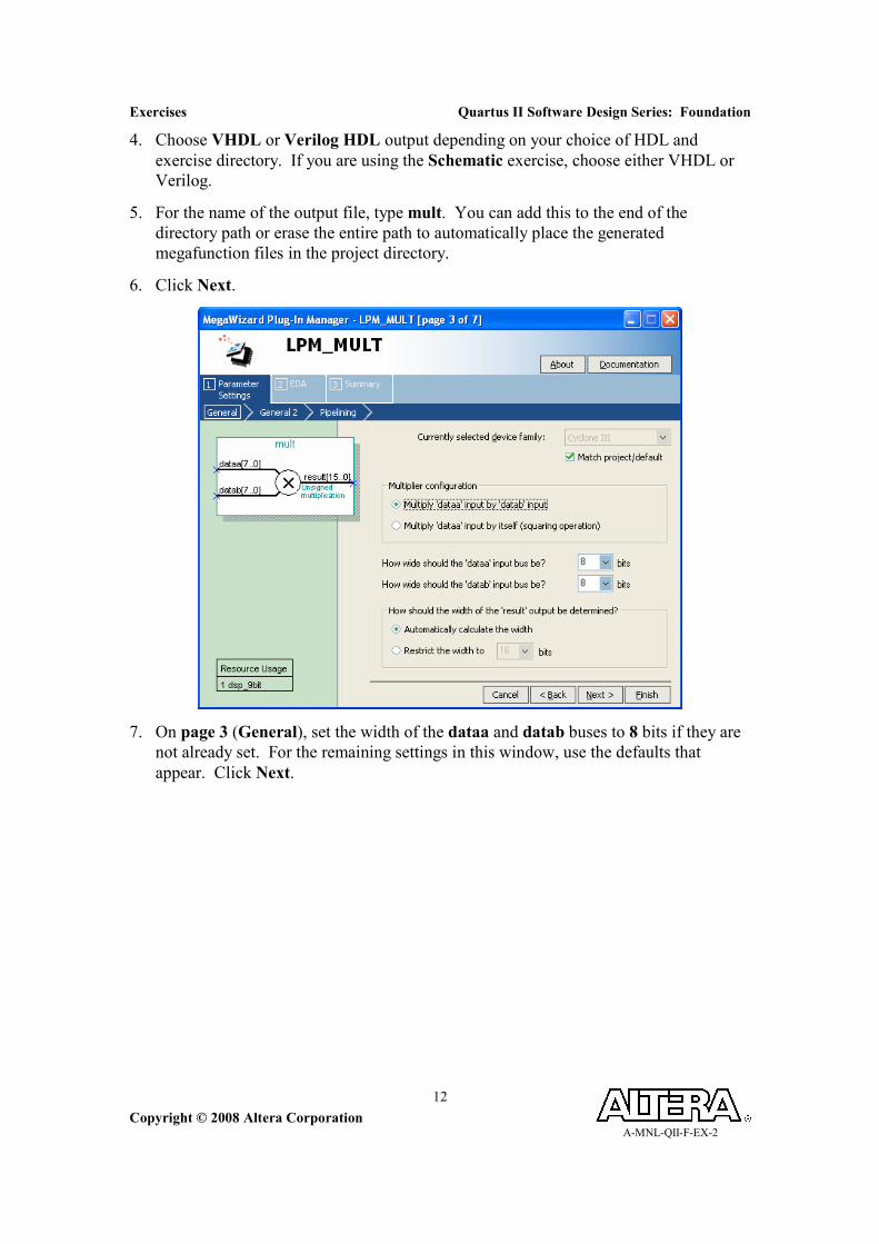
7. On page 3 (General), set the width of the dataa and datab buses to 8 bits if they are
not already set. For the remaining settings in this window, use the defaults that
appear. Click Next.

Quartus II Software Design Series: Foundation Exercises
Copyright © 2008 Altera Corporation A-MNL-QII-F-EX-2
13
8. On page 4 (General 2), use all the default settings (i.e. datab input does NOT have a
constant value, use unsigned multiplication, and select the default multiplier
implementation). Click Next.
9. On page 5 (Pipelining), choose Yes, I want an output latency of 2 clock cycles.
Click Next.

Exercises Quartus II Software Design Series: Foundation
Copyright © 2008 Altera Corporation A-MNL-QII-F-EX-2
14
10. You should now be on page 6 (section 2 of the MegaWizard called EDA). This tab
indicates the simulation model file needed to simulate LPM_MULT in an EDA
simulation tool (e.g. the ModelSim-Altera tool). The lpm simulation model file
should be indicated as shown above. You also have the option of generating an early
netlist for use by a 3rd-party synthesis tool. We are not using any third-party tools, so
just click Next.

Quartus II Software Design Series: Foundation Exercises
Copyright © 2008 Altera Corporation A-MNL-QII-F-EX-2
15
11. On page 7, the following check boxes should be enabled to generate output files
according to Table 2 below:
Table 2. MegaWizard files to generate
12. Click Finish to create the megafunction. If a dialog box appears asking about the
creation of a Quartus II IP File, click Yes.
The multiplier is built.
If for some reason your megafunction is incorrect or you forgot or missed a checkbox
for generating all the required output files, open the MegaWizard Plug-In Manager
again from the Tools menu or Tasks window. Select to edit an existing megafunction,
and go through the pages of the MegaWizard again (skip around with the tabs at the
top) to fix your mistakes or generate the missing file(s). Click Finish to update the
megafunction or files.
Design Entry Method Files to Enable in MegaWizard Plug-In
VHDL mult.vhd, mult.cmp & mult_inst.vhd
Verilog mult.v & mult_inst.v
Schematic mult(.vhd or .v) & mult.bsf

Exercises Quartus II Software Design Series: Foundation
Copyright © 2008 Altera Corporation A-MNL-QII-F-EX-2
16
Step 2: Create a 32x16 RAM using the MegaWizard Plug-In Manager
1. Open the MegaWizard Plug-In Manager again (Tools or Tasks window ⇒⇒⇒⇒
MegaWizard Plug-In Manager). Select to Create a new custom megafunction
variation, and click Next.
2. Select the megafunction to create. On page 2a (shown above), expand the Memory
Compiler folder and select RAM: 2-PORT.
3. As before, choose the Cyclone III device family and VHDL or Verilog HDL.
4. For the name of the output file, enter ram.
5. Click Next.

Quartus II Software Design Series: Foundation Exercises
Copyright © 2008 Altera Corporation A-MNL-QII-F-EX-2
17
6. On page 3, select With one read port and one write port in the section for how you
will be using the dual port ram. For the remaining setting in this window, use the
default (memory size specified as a number of words). Click Next.
7. On page 4 (Widths/Blk Type), set the width of the Read/Write Ports for the data_a
input to 16. Then choose 32 as the number of 16-bit words of memory. (Note: This
will read “8-bit words of memory” until you change the width of the read/write ports.)
Leave the memory block type selection set to its default of Auto. Click Next 2 times.

Exercises Quartus II Software Design Series: Foundation
Copyright © 2008 Altera Corporation A-MNL-QII-F-EX-2
18
8. On page 6 (Regs/Clkens/Aclrs), disable the option to register the Read output
port(s) ‘q’. Accept the remaining default settings, and click Next 2 times.
9. On page 8 (Mem Init), click Yes that you have a file to use for the memory content
data. Once enabled, type in the file name ram.hex. We’ll be creating this file next,
but we can enter it now so we don’t have to go back into the MegaWizard later. Click
Next.
10. On page 9, the altera_mf simulation model file is displayed as being needed to
simulate this function in a 3rd-party EDA simulation tool. Click Next.

Quartus II Software Design Series: Foundation Exercises
Copyright © 2008 Altera Corporation A-MNL-QII-F-EX-2
19
11. Choose the same file extensions for ram as you selected for mult earlier (Step 1,
#11). Click Finish.
You have now created the two components needed for this design. Now you will
create the HEX file needed to initialize the contents of the RAM.
Step 3: Create HEX file using Memory Editor
1. From the Tasks window, in the Create Design folder, double-click Create New
Design File. You could also go to the File menu and select New or click in the
toolbar.
2. In the New dialog box, expand the Memory Files category and select Hexadecimal
(Intel-Format) File. Click OK.
3. In the memory size dialog box, choose 32 as the number of words and 16 as the
word size. Click OK.

Exercises Quartus II Software Design Series: Foundation
Copyright © 2008 Altera Corporation A-MNL-QII-F-EX-2
20
The Memory Editor now displays your memory space. If your memory space is not
displayed exactly as above, change the number of cells per row (View menu) to 16
and the memory radix (View menu) to Hexadecimal.
4. Highlight all of the memory locations in your memory space. Right-click and select
Custom Fill Cells.
5. Use the Custom Fill Cells dialog box to enter your own values to initialize your
memory. You can enter any values you want. Do one of the following:
a. Repeating Sequence: Enter a series of numbers separated by commas or
spaces to be repeated in memory.
b. Incrementing/Decrementing: Enter a start value and another value by which to
increment or decrement the start value.
6. Save the file as ram.hex. Close ram.hex.

Quartus II Software Design Series: Foundation Exercises
Copyright © 2008 Altera Corporation A-MNL-QII-F-EX-2
21
Step 4: Instantiate and connect design blocks according to design entry method
1. Open pipemult.bdf. You can use the Open command from the File menu, click the
toolbar button, or double-click the entity in the Project Navigator. You can also
double-click Open Existing Design File in the Create Design folder of the Tasks
window.
This is the top-level schematic file for the design. Normally, you would have to
instantiate both ram and mult subdesigns and connect them together manually. In
the interest of time, the schematic file has been almost completed for you, but it is
missing the ram and mult blocks and the output pins q[15..0].
2. In the schematic file, double-click any empty area so that the Symbol window
appears. Inside the Symbol window, click to expand the symbols defined in the
Project folder. Double-click the mult symbol. Click the left mouse button to place
the symbol inside the schematic file where indicated.
Note: The three ports on the left side of the multiplier should line up exactly with the
wires coming from the input pins (no X’s). If not, you may not have specified the
multiplier parameters correctly when configuring the megafunction. If this is the
case, hit the Esc key to cancel the symbol placement, reopen the MegaWizard Plug-In
Manager, and select Edit an existing megafunction variation to open and edit the
mult megafunction to fix the problem and regenerate the symbol.
3. Right-click on the mult symbol and choose Properties. In the Symbol Properties
dialog box, change the Instance name: from inst to mult_inst. Click OK.
4. Double-click an open area again to reopen the Symbol window. This time, select the
ram symbol and place it in the schematic file where indicated.
Note: With ram, the lower 4 ports on the left side of the symbol should line up with
the wires coming from the input pins. The data port should be unconnected.
5. As you did with mult, use the Symbol Properties dialog box to change the name of
the ram instantiation from inst to ram_inst.
6. Open the Symbol window again and this time, type output in the Name: field.
The Symbol window found the output symbol automatically by name.
7. Click OK and place the output pin near the output port of the inst2 register symbol.
Double-click the pin_name and change it to q[15..0].
8. Click on the bus drawing tool , found in the schematic editor toolbar, and draw
the bus connections between mult (result) and ram (data).
Exercises Quartus II Software Design Series: Foundation
Copyright © 2008 Altera Corporation A-MNL-QII-F-EX-2
22
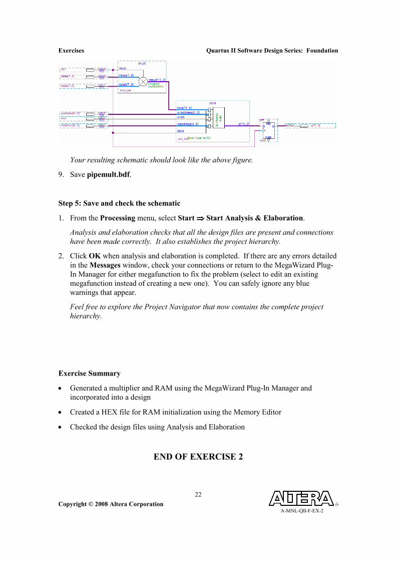
Your resulting schematic should look like the above figure.
9. Save pipemult.bdf.
Step 5: Save and check the schematic
1. From the Processing menu, select Start ⇒⇒⇒⇒ Start Analysis & Elaboration.
Analysis and elaboration checks that all the design files are present and connections
have been made correctly. It also establishes the project hierarchy.
2. Click OK when analysis and elaboration is completed. If there are any errors detailed
in the Messages window, check your connections or return to the MegaWizard Plug-
In Manager for either megafunction to fix the problem (select to edit an existing
megafunction instead of creating a new one). You can safely ignore any blue
warnings that appear.
Feel free to explore the Project Navigator that now contains the complete project
hierarchy.
Exercise Summary
• Generated a multiplier and RAM using the MegaWizard Plug-In Manager and
incorporated into a design
• Created a HEX file for RAM initialization using the Memory Editor
• Checked the design files using Analysis and Elaboration
END OF EXERCISE 2

Quartus II Software Design Series: Foundation Exercises
Copyright © 2008 Altera Corporation A-MNL-QII-F-EX-2
23
Exercise 3

Exercises Quartus II Software Design Series: Foundation
Copyright © 2008 Altera Corporation A-MNL-QII-F-EX-2
24
Exercise 3
Objectives:
• Perform full compilation
• Locate information in the Compilation Report
• Explore cross-probing capabilities by viewing logic in various windows

Quartus II Software Design Series: Foundation Exercises
Copyright © 2008 Altera Corporation A-MNL-QII-F-EX-2
25
Compilation Report
Device Name EP3C5F256C6
Total Design
Total Logic Elements
Total Memory Bits
Total Embedded Multiplier 9-Bit Elements
Total Pins
mult subdesign
Logic Cells (mult)
Dedicated Logic Registers (mult)
Memory Bits (mult)
M9Ks (mult)
DSP Elements (mult)
ram subdesign
Logic Cells (ram)
Dedicated Logic Registers (ram)
Memory Bits (ram)
M9Ks (ram)
DSP Elements (ram)
Control signals & fan-out

Exercises Quartus II Software Design Series: Foundation
Copyright © 2008 Altera Corporation A-MNL-QII-F-EX-2
26
Step 1: Compile the design
1. Select Start Compilation from the Processing menu or click located on the
toolbar to perform a full compilation of the design. You can also double-click
Compile Design in the Tasks window. A dialog box will appear when the
compilation is complete.
2. Click OK.
Step 2: Gather information from the Compilation Report)
The Compilation Report provides all information on design processing. You use it to
understand how the compiler interpreted your design and to verify results. It is
organized by compiler executables, with each one generating its own folder. By
default, the Compilation Report opens when any processing begins and displays the
Flow Summary Section when that process finishes.
1. From the Flow Summary section of the Compilation Report, record the Total logic
elements, total memory bits, total embedded multiplier 9-bit elements and total
pins in the table at the beginning of this exercise.
From these results, you can see that this design is currently using only dedicated
device resources (i.e. embedded memory, embedded multipliers) and no logic other
than the registers included within these resources.
2. Expand the Fitter folder in the Compilation Report. Locate the Resource Section
folder. From the Resource Utilization by Entity table, record in the exercise table
the requested resource counts for the mult and ram subdesigns.
3. From the Control Signals table, record the control signals found and their fan-out.
Though the clock in this design obviously drives more than 3 registers, the fan-out of
3 refers to the number of architectural blocks it drives: 1 memory block, 1 embedded
multiplier, and 1 set of output registers. But registers should be counted as used
logic elements, shouldn’t they? Why does the compilation report indicate that no
logic elements are being used by the design?
In the next few steps, you will take a look at some additional ways to analyze the
results of your compilation and determine the location of the output registers.
Step 3: Explore the design logically using the RTL Viewer
The RTL Viewer allows you to view a logical representation of an analyzed design
graphically. It is a very helpful tool for debugging HDL synthesis results.
1. From the Tools menu, open the RTL Viewer (under Netlist Viewers). You can also
access the RTL Viewer from the Compile Design section of the Tasks window.

Quartus II Software Design Series: Foundation Exercises
Copyright © 2008 Altera Corporation A-MNL-QII-F-EX-2
27
You should see the diagram shown above. This is a graphical view displaying the
logical representation of the design. Currently it shows the I/O, the instantiation of
the mult and ram subdesigns, and an additional set of output registers. Notice the
registers are external to the memory block per the original design. The output
register block is named inst2[15..0] in the schematic version of the project, but the
rest of the diagram is the same for all three versions.
2. Select the ram subdesign to highlight it. The outline of the block turns bright red
when the block is selected. Right-click and select Ungroup Selected Nodes.
The ram block is now displayed with all of the input and output buses expanded. This
operation is helpful when you want to see how individual bits are connected. This
operation can be performed on internal blocks and I/O.
3. Select the ram subdesign again if it was deselected. Right-click and select Group
Related Nodes.
This returns the RTL Viewer to the previous view.
4. Double-click on the ram subdesign block.

Exercises Quartus II Software Design Series: Foundation
Copyright © 2008 Altera Corporation A-MNL-QII-F-EX-2
28
You have now descended the hierarchy into the ram subdesign. As a result, the view
changes to the above or similar image (may appear slightly different for VHDL).
This shows that the ram subdesign is made up of a single megafunction block called
altsyncram. You can continue double-clicking blocks to descend the hierarchy to its
lowest level: single-bit RAM functions. Let’s view this lowest level of the hierarchy in
a different way.
5. Double-click in any empty space.
This returns the viewer to the top-level view of the design. If you’ve descended
further into the hierarchy, you may need to do this a few times to return to the top.
6. Select the ram subdesign again. Right-click and select Display Content.
Instead of displaying the lower hierarchical level alone, the Display Content option
displays the lower level within the current hierarchy logic (may appear differently
than above for VHDL). The green box (currently highlighted in red) around the
altsyncram subdesign indicates a hierarchical boundary.

Quartus II Software Design Series: Foundation Exercises
Copyright © 2008 Altera Corporation A-MNL-QII-F-EX-2
29
7. Select the altsyncram module, right-click, and select Display Content.
Descending the hierarchy again, the internal logic of the altsyncram module
(altsyncram_psp1) is displayed including module I/O that are not connected.
8. Select the altsyncram_psp1 module, right-click, and select Display Content. Zoom
out with the magnifying glass tool (right-click) if necessary.
Moving down into the altsyncram_psp1 module, the viewer indicates that this module
is represented by 16 smaller RAM functions, one function for each input/output data
bit. Remember, this is a FUNCTIONAL representation of the design, not how the
design will ultimately be implemented in the target Cyclone III device.

Exercises Quartus II Software Design Series: Foundation
Copyright © 2008 Altera Corporation A-MNL-QII-F-EX-2
30
Notice also in the RTL Viewer that the Hierarchy List shows how we have descended
down into the ram subdesign. For each hierarchical level, you can also see the
names of its pins and nets.
Quartus II Software Design Series: Foundation Exercises
Copyright © 2008 Altera Corporation A-MNL-QII-F-EX-2
31
Step 4: Explore the ram subdesign physically using the Technology Map Viewer
The Technology Map Viewer allows you to see how a design is actually implemented
using FPGA/CPLD resources. Use this tool as an aid during constraining and
debugging to see changes in resource usage as settings and options are adjusted.
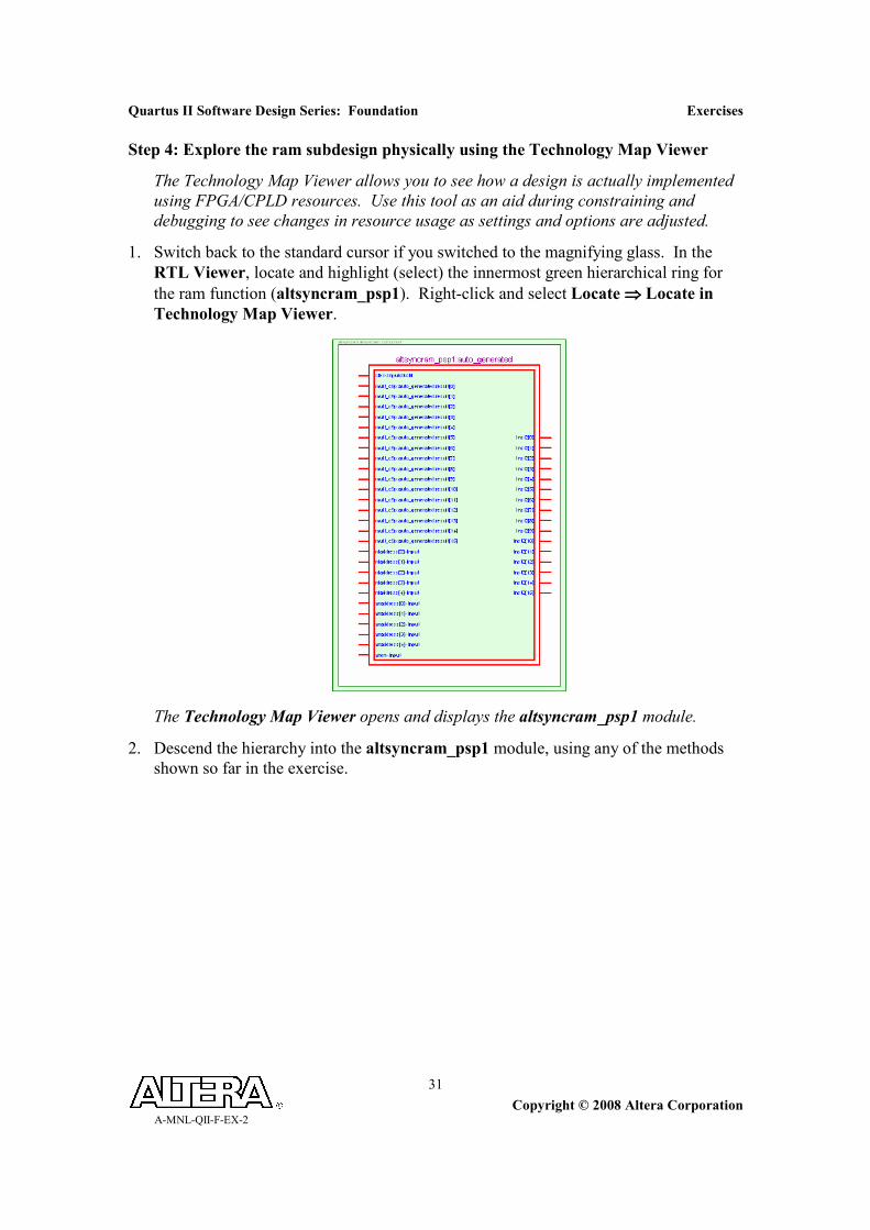
1. Switch back to the standard cursor if you switched to the magnifying glass. In the
RTL Viewer, locate and highlight (select) the innermost green hierarchical ring for
the ram function (altsyncram_psp1). Right-click and select Locate ⇒⇒⇒⇒ Locate in
Technology Map Viewer.
The Technology Map Viewer opens and displays the altsyncram_psp1 module.
2. Descend the hierarchy into the altsyncram_psp1 module, using any of the methods
shown so far in the exercise.

Exercises Quartus II Software Design Series: Foundation
Copyright © 2008 Altera Corporation A-MNL-QII-F-EX-2
32
Now, instead of showing the 16 functional memory blocks as shown in the RTL
Viewer, the Technology Map Viewer displays the ACTUAL device resource that was
used, a single RAM block (ram_block1a0).
3. Double-click on the ram_block1a0 to view the detailed implementation of the
memory block.
From this view you can see all the inputs to the RAM are registered as well as the
output. The output? Weren’t the output registers outside of the memory block in the
RTL Viewer? And didn’t we turn off the use of output registers on the q outputs
when we created the RAM megafunction? Even so, the fitter has moved those
registers into the memory block to improve memory block performance and design
density. This behavior is called register packing, and the Fitter does this to help save
device resources. There is a fitter-generated “Extra Info” message in the Message
window (possibly in the Suppressed tab) that also indicates this optimization was
performed.
This could be further verified by viewing ram_block1a0 in the Resource Property
Editor (right-click and select from the Locate submenu).
4. Click the back toolbar button to return to the view of the RAM block.
Step 5: Use the Chip Planner to view connections to the ram subdesign
The Chip Planner will give you a sense of where logic has been placed in the design.
This can be very helpful when trying to understand design performance, as proximity
is the key to performance in most newer FPGAs and CPLDs. Though the Chip

Quartus II Software Design Series: Foundation Exercises
Copyright © 2008 Altera Corporation A-MNL-QII-F-EX-2
33
Planner can be used for manually locating and moving logic, we currently only want
to evaluate results.
1. In the Technology Map Viewer, select the RAM block (ram_block1a0) to highlight
it. Right click and select Locate ⇒⇒⇒⇒ Locate in Chip Planner (Floorplan & Chip
Editor).
2. In the Chip Planner, use the zoom tool (Chip Planner toolbar) and right-click to
zoom out a few times.
You should now see the ram subdesign (highlighed in blue) and where it has been
placed in the Cyclone III device. The other shaded areas in the Chip Planner are
where the remaining logic has been placed. Since we don’t have any constraints
applied to the design, the fitter was free to place logic anywhere. This will change
later.
3. With the memory block highlighted in the Chip Planner, click the Generate Fan-In
Connections toolbar button . Click Yes on any confirmation dialog that may
appear.
The Chip Planner now displays the device resources that are feeding into the ram
subdesign (device I/O and the multiplier). Delays incurred between them for rising
and falling edges of the signals may be available (as seen on the next page).
4. Select the ram subdesign in the Chip Planner again (you may need to zoom back in a
little), and click the Generate Fan-Out Connections button .

Exercises Quartus II Software Design Series: Foundation
Copyright © 2008 Altera Corporation A-MNL-QII-F-EX-2
34
The Chip Planner now displays both fan-in and fan-out connections. The fan-out
connections are displayed in blue.
5. Turn off the fan-in/fan-out by clicking on any non-highlighted part of the device and
then clicking the Clear Unselected Connections/Paths toolbar button .
6. Close the RTL Viewer, Technology Map Viewer, and Chip Planner.
Exercise Summary
• Performed a full compilation
• Gathered information from the compilation report
• Cross-probed between windows to analyze design processing results in different ways
using the RTL Viewer, Technology Map Viewer, & Chip Planner
END OF EXERCISE 3

Quartus II Software Design Series: Foundation Exercises
Copyright © 2008 Altera Corporation A-MNL-QII-F-EX-2
35
Exercise 4

Exercises Quartus II Software Design Series: Foundation
Copyright © 2008 Altera Corporation A-MNL-QII-F-EX-2
36
Exercise 4
Objectives:
• Assign I/O pins and perform I/O Assignment Analysis
• Use the Pin Migration View to see the effect of device migration on I/O assignments

Quartus II Software Design Series: Foundation Exercises
Copyright © 2008 Altera Corporation A-MNL-QII-F-EX-2
37
Step 1: Use Pin Planner to assign I/O pins & set I/O standards
1. From the Assignments menu or the Assign Constraints folder of the Tasks window,
open the Pin Planner.
Remember that you can detach the Pin Planner from the main Quartus II application
window to make it bigger, as well as undock the Groups and All Pins lists.
2. Make sure the Top View of the device is displayed. If not, select Package Top from
the View menu.
3. In the Pin Planner toolbar, make sure that the Show I/O Banks toolbar button
has been enabled. If you are unsure of which button this is, you can also find this
option in the View menu.
4. Turn on the Live I/O checking feature to perform limited checks on your I/O
assignments you’ll be making in the following steps. To do this, click in the
toolbar or select Enable Live I/O Check from the Processing menu in the Pin
Planner.
The Live I/O Check icon will appear in the Package view to indicate the feature is
turned on.
5. From the View menu in the Pin Planner, select Live I/O Check Status Window.
This opens a small floating window that alerts you to I/O assignment errors and
warnings as you make assignments. Be sure to watch this window during the
following steps. If the status indicates an error or warning, check the Messages
window in the main Quartus II window for information.

Exercises Quartus II Software Design Series: Foundation
Copyright © 2008 Altera Corporation A-MNL-QII-F-EX-2
38
6. In the Groups List window of the Pin Planner, locate the dataa input bus, and click
it once to select it. Then, click and drag the dataa bus from the Groups List
window and drop it into the IOBANK_7 box of the Package View (the top right side
of the chip).
The display for IOBANK_7 will now change to indicate that I/O Bank 7 has 8
assigned pins out of 26 total pins. Assigning signals to an I/O bank like this gives the
Fitter the freedom to place the signals anywhere within the specified I/O bank.
7. In the Groups List, right-click on the dataa bus and select Node Properties.
8. In the Node Properties dialog box, set the I/O standard for dataa to 1.8 V. Click
OK.
Notice that the All Pins list reflects the I/O standard change for all of the individual
dataa pins. You could have assigned the location and changed the I/O standard
using the All Pins list as well. However, be aware that individual assignments made
in the All Pins list (or on individual signals within groups in the Groups list) take
precedence over group assignments made in the Groups list. The best way to ensure

Quartus II Software Design Series: Foundation Exercises
Copyright © 2008 Altera Corporation A-MNL-QII-F-EX-2
39
that all the signals in an entire bus or signal group inherit an assignment like this is
to make the assignment to the group heading (i.e. dataa[7..0]) in the Groups list.
9. Using either the Package View or the All Pins List, assign the datab bus to
IOBANK_7.
You may notice something going on with the Live I/O Check status window. Be sure
to check it out and look at the Messages window. For now, though, don’t try to fix
the problem. We want to see how the compiler handles this.
10. Assign the q output bus to IOBANK_5 (lower I/O bank on the right side of the chip)
and set the I/O standard to 1.8 V.
11. Assign both the rdaddress and wraddress buses to IOBANK_6 (upper I/O bank on
the right side of the chip) and set the I/O standard to 1.8 V.
12. Using the All Pins List, assign clk1 to Pin E15 and set the I/O standard to 1.8 V.
13. Using the All Pins list, assign wren to IOBANK_5 and set the I/O standard to 1.8
V.
Your Pin Planner should look similar to the above picture.
Exercises Quartus II Software Design Series: Foundation
Copyright © 2008 Altera Corporation A-MNL-QII-F-EX-2
40
Step 2: Analyze I/O assignments
Now that you have made general I/O assignments, you can check the validity of those
assignments without running a full compilation. This way you can quickly and easily
find I/O placement issues and correct them. This will check more I/O rules than the
live I/O check, so be sure to always run I/O Assignment Analysis even if you are using
the live I/O checking feature.
1. From the Processing menu in the main Quartus II window, go to Start and select
Start Analysis & Synthesis or click on the button in the main Quartus II toolbar.
Click OK when complete.
The compiler may turn off live I/O checking and then turn it back on. If it ever leaves
it turned off after a compilation process, simply turn it back on in the Pin Planner.
2. From the Processing menu, go to Start and select Start I/O Assignment Analysis or
click on the button in the Pin Planner toolbar. Click OK once the analysis is
complete.
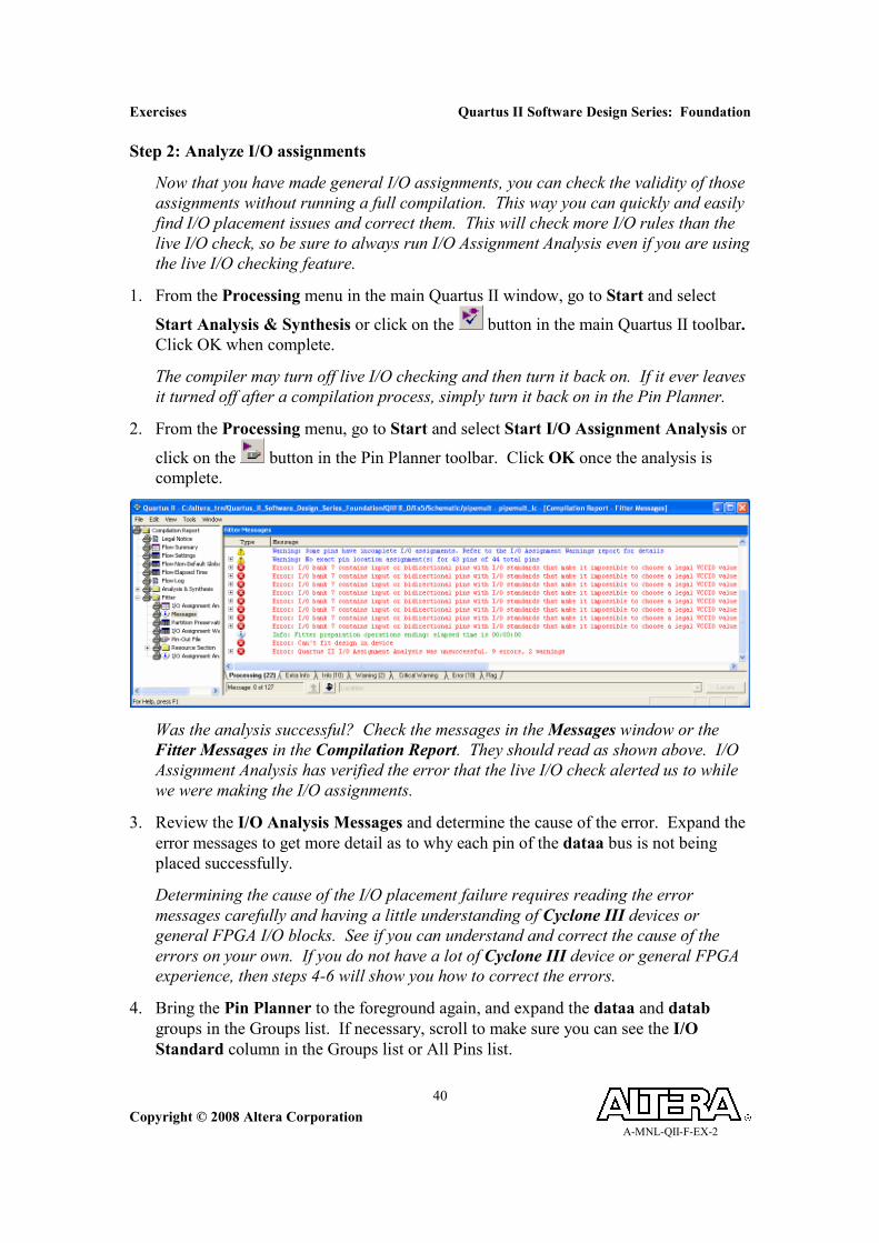
Was the analysis successful? Check the messages in the Messages window or the
Fitter Messages in the Compilation Report. They should read as shown above. I/O
Assignment Analysis has verified the error that the live I/O check alerted us to while
we were making the I/O assignments.
3. Review the I/O Analysis Messages and determine the cause of the error. Expand the
error messages to get more detail as to why each pin of the dataa bus is not being
placed successfully.
Determining the cause of the I/O placement failure requires reading the error
messages carefully and having a little understanding of Cyclone III devices or
general FPGA I/O blocks. See if you can understand and correct the cause of the
errors on your own. If you do not have a lot of Cyclone III device or general FPGA
experience, then steps 4-6 will show you how to correct the errors.
4. Bring the Pin Planner to the foreground again, and expand the dataa and datab
groups in the Groups list. If necessary, scroll to make sure you can see the I/O
Standard column in the Groups list or All Pins list.

Quartus II Software Design Series: Foundation Exercises
Copyright © 2008 Altera Corporation A-MNL-QII-F-EX-2
41
Notice that you have assigned the dataa and datab input buses to I/O Bank 7 but set
different VCCIO (1.8 & 2.5) voltage levels for them. Cyclone III FPGAs, like all
Altera FPGA devices, allow for only one VCCIO per I/O bank.
5. Using the Groups List, change the I/O standard setting for the dataa group to 2.5 V
(or 2.5 V (default)). Make sure the dataa group as well as each individual signal in
the group is set to 2.5 V.
In the Groups list, signals have individual assignments as well as group assignments,
and individual or group assignments are not automatically inherited by each other
(i.e. setting all the individual signals in dataa to 2.5 V does not automatically set the
group assignment, dataa[7..0], to 2.5 V), so make sure that both the group and
individual assignments are all set the same.
Tip: Try changing the I/O standard for just dataa[7..0] in the Groups List and placing
your cursor at the lower right corner of the I/O Standard cell for this signal. You
can use auto-fill, a standard spreadsheet operation, to fill in the changed I/O
standard for the rest of the dataa bus located below dataa[7..0] if you’ve accidentally
created any individual assignments for signals within the dataa bus.
Notice the change in the Live I/O Check Status window.
6. Re-run I/O Assignment Analysis. Click OK when complete.
See how quickly and easily you can check your I/O placement assignments without
running a full compilation!
7. To see where the Fitter placed your I/O, click on the button in the Pin Planner
toolbar or from the View menu choose Show ⇒⇒⇒⇒ Show Fitter Placements. Click OK
to turn off live I/O checking.
Live I/O checking must be turned off when viewing Fitter placements. The status
window confirms that it is off.

Exercises Quartus II Software Design Series: Foundation
Copyright © 2008 Altera Corporation A-MNL-QII-F-EX-2
42
You can see that fitter-selected pins appear in green in the Pin Planner as shown
above. Notice that clk1, the only signal you manually assigned to a specific pin
(E15), appears green with a red hatched pattern. Remember that this indicates that
your user assignment matches up with the location assignment made by the Fitter.

Quartus II Software Design Series: Foundation Exercises
Copyright © 2008 Altera Corporation A-MNL-QII-F-EX-2
43
Step 3: Back-annotate pin assignments to lock placement
At this point, you like the I/O location assignments made by the Fitter, and you’ve
verified the pin-out to begin board design. Now you need to make sure that the pin
locations are not moved during successive compilations.
1. From the Assignments menu, select Back-Annotate Assignments to open the Back-
Annotate Assignments dialog box. The dialog box may appear slightly different
from the screenshot below.
2. In Assignments to back-annotate, enable Pin & device assignments (default
setting) as shown above. Click OK.

Exercises Quartus II Software Design Series: Foundation
Copyright © 2008 Altera Corporation A-MNL-QII-F-EX-2
44
Notice how all the I/O pins that were green earlier have changed to the green and red
hatch pattern. This indicates that the locations that were fitter-assigned I/O are now
user-assigned I/O and have been written into your .QSF file as constraints.
3. Remove the group I/O assignments. For each I/O Bank box in the Package view,
click it and press Delete to remove the group assignments.
Since back-annotation has locked in the individual assignments, we no longer want or
need the group assignments we made earlier.
Exercise Summary
• Assigned pin locations using the Pin Planner
• Back-annotated pin locations from prior compilation
• Verified I/O placement and constraints using I/O assignment analysis
END OF EXERCISE 4

Quartus II Software Design Series: Foundation Exercises
Copyright © 2008 Altera Corporation A-MNL-QII-F-EX-2
45
Exercise 5

Exercises Quartus II Software Design Series: Foundation
Copyright © 2008 Altera Corporation A-MNL-QII-F-EX-2
46
Exercise 5
Objectives:
• Follow the steps to using the TimeQuest timing analyzer
• Apply constraints to a design using the SDC file editor and the TimeQuest GUI
• create_clock
• set_input_delay
• set_output_delay
Table 3
Worst Setup
Slack
(fast, slow, or
slow 0°°°°C model)
Worst Hold
Slack
(fast, slow, or
slow 0°°°°C model)
pipemult revision

Quartus II Software Design Series: Foundation Exercises
Copyright © 2008 Altera Corporation A-MNL-QII-F-EX-2
47
Step 1: Synthesize the design
1. Verify that you are using the pipemult revision and click to synthesize the design.
Though you could also perform a full compilation, performing synthesis allows you to
quickly generate a netlist in order to start constraining. And even though the
pipemult revision has been previously compiled, we want to highlight the
recommended tool flow.
Step 2: Start the TimeQuest GUI and set up timing netlist for analysis
1. From the main Quartus II toolbar, click or, from the Tools menu, select
TimeQuest Timing Analyzer. You can also start the timing analyzer from the Tasks
window (Compile Design folder). Click No that you do not want to generate a .SDC
file from a .QSF file. If you accidentally click Yes, close the TimeQuest interface,
open an Explorer window, and delete the pipemult.sdc file that got created in your
project directory. Return to the Quartus II software and open the TimeQuest interface
again.
The window above opens. You will now go through the steps to use the TimeQuest
timing analyzer in the Quartus II design flow.

Exercises Quartus II Software Design Series: Foundation
Copyright © 2008 Altera Corporation A-MNL-QII-F-EX-2
48
2. Create a timing netlist. From the Netlist menu, select Create Timing Netlist and
change the Input netlist type to Post-map. Click OK.
A green checkmark appears next to Create Timing Netlist in the Tasks pane to
indicate the command was successful. You could also have double-clicked Create
Timing Netlist in the Tasks pane, but that would have defaulted to creating a post-fit
netlist, so it was not used in this case.
3. Read an SDC file. Simply click at the tcl> prompt in the Console pane and type
read_sdc.
A message appears indicating that an SDC file has not been found. This is correct.
Since you did not specify a filename, the timing analyzer automatically looked for any
SDC files that were added to the project and then an SDC file sharing the same name
as the current revision pipemult, neither of which exists yet.
There should now be a green checkmark next to Read SDC File indicating you tried
to read an SDC file. You’ll now create an SDC file using the SDC file editor (same
as the Quartus II text editor) and the TimeQuest GUI.

Quartus II Software Design Series: Foundation Exercises
Copyright © 2008 Altera Corporation A-MNL-QII-F-EX-2
49
Your Tasks pane should look like the screenshot above at this point.
Step 3: Create a .sdc file and add a clock constraint
1. From the File menu in Timequest, select New SDC File. The SDC file editor will
open with a new, empty file.
2. From the File menu in the SDC file editor, select Save As and name the SDC file
pipemult.sdc.
Notice that Add file to current project is enabled by default in the Save As dialog
box.
3. Use the Create Clock command to add a 6 ns clock constraint to the clk1 input.
a. From the Edit menu in the SDC file editor, go to Insert Constraint and select
Create Clock…
b. In the Create Clock dialog box, type clk1 as the clock name.
We are using the same name as the clock node, but you can name the clock
whatever you want.
c. In the period field, type 6.
Notice you can enter the waveform edges to create a non-50% duty-cycle clock.
We will leave that blank since this clock’s duty cycle is 50%.
d. In the targets field, click on the browse button .
This opens the Name Finder window.
e. In the Name Finder, choose get_ports from the Collection drop-down menu. In
the Matches section, click List.
f. Double-click on clk1 in the list of matches.

Exercises Quartus II Software Design Series: Foundation
Copyright © 2008 Altera Corporation A-MNL-QII-F-EX-2
50
Notice the bottom of the dialog box shows the SDC collection command for the
target you selected.
g. Click OK.
The Create Clock dialog box should appear as shown above. Again at the
bottom, the SDC equivalent command for the options set is displayed.
h. Click Insert. Save the file.

Quartus II Software Design Series: Foundation Exercises
Copyright © 2008 Altera Corporation A-MNL-QII-F-EX-2
51
Your clock constraint gets added to the SDC file at the cursor location. At this point,
we’ll update the timing netlist to make sure that the remaining constraints we create
recognize this clock.
4. Back in the TimeQuest main window, double-click Update Timing Netlist in the
Tasks pane. Return to or reopen your SDC file.
Step 4: Add I/O constraints
1. On a new line in the file (remember, the GUI inserts commands wherever the cursor is
located), use the Set Input Delay command to set a maximum input delay of 4.5 ns
to both 8-bit input buses dataa and datab, with respect to clk1.
a. From the Insert Constraint submenu in the Edit menu, select Set Input Delay.
b. Fill in the window with the following information:
Clock name = clk1 (use drop-down)
Input Delay Options = Maximum (leave Rise/Fall to Both)
Delay Value = 4.5
Targets = [get_ports data*]
You could have used the browse button and Name Finder to locate all of the data
inputs (like you did with clk1), but sometimes, especially with buses, it is just
easier to type in a command directly and use wildcards. If you didn’t know the
name of the bus, you could still use the Name Finder and add the wildcard in the
Name Finder SDC command field after selecting the signals that make up the bus.

Exercises Quartus II Software Design Series: Foundation
Copyright © 2008 Altera Corporation A-MNL-QII-F-EX-2
52
Your Set Input Delay dialog box should look like the screenshot above.
c. Click Insert.
2. Use the Set Input Delay command to set a minimum input delay of 1.75 ns to both
8-bit input buses dataa and datab, with respect to clk1. To do this quickly, use copy
and paste to make a copy of the maximum input delay command on the next line.
Edit the line to change –max to –min and 4.5 to 1.75.
3. Similar to the above, use the Set Output Delay command to set a maximum output
delay of 0.7 ns to the 16-bit q output bus, with respect to clk1. Using a wildcard here
will be very handy.
4. Use the Set Output Delay command again to set a minimum output delay of 0.0 ns
to the 16-bit q output bus, with respect to clk1.
5. Use the Set Input Delay command again to constrain all rdaddress and wraddress
inputs to a maximum delay of 2.5 ns and a minimum of 1.0 ns, with respect to clk1.
6. Save the file.
Step 5: Update the timing netlist
1. To let TimeQuest know that we’ve added new constraints, we’ll create a new timing
netlist and update it. From the Netlist menu in the main TimeQuest window, select
Delete Timing Netlist.
2. Again from the Netlist menu, create a new, post-map netlist.
3. Update the timing netlist with the constraints we added to the SDC file. In the Tasks
pane of the TimeQuest GUI, double-click Update Timing Netlist.

Quartus II Software Design Series: Foundation Exercises
Copyright © 2008 Altera Corporation A-MNL-QII-F-EX-2
53
You could have performed the Read SDC File task manually before updating the
netlist, but skipping to updating the netlist automatically reads in the SDC file we
created and saved with the project revision’s name.
Step 6: Use TimeQuest reports to verify all constraints entered correctly
Now that the netlist has been updated, you can begin generating various reports. The
first ones you want to run are to check the timing constraints you entered.
1. In the Tasks pane, double-click Report SDC.
In the Report pane, a new folder called SDC Assignments appears containing three
reports called Create Clock, Set Input Delay and Set Output Delay. Do these look
like all of the constraints that you entered?
2. In the Tasks pane, double-click on Report Clocks.
Use this report to verify that your clock(s) have been entered correctly and applied to
the correct ports or pins.
3. In the Tasks pane, double-click on Report Ignored Constraints.
This report will list any constraints that you entered that were ignored by the timing
analyzer. For example, if you typed an incorrect port name that caused your SDC
command to be ignored, it would appear in the Ignored Constraints folder. Are any
of your constraints showing up as ignored that should not be? If so, go back to the
SDC file, fix the errors, recreate and update the netlist, then regenerate the reports.
4. In the Tasks pane, double-click on Report Unconstrained Paths.
Use this report to ensure you have a fully constrained design. Are there any missing
constraints? If so, what is missing?
5. Look through the reports in the Unconstrained Paths report folder to see what is
missing.
The Unconstrained Paths Summary (in red) should indicate to you that 1 input port
and 16 input port path have been left unconstrained. Open the Setup Analysis and
Hold Analysis folders to verify which port/path they are.
Do you see that the wren input port is not constrained? Because of this, the paths
from the wren port to the write enable input registers for ram are also
unconstrained.
6. Return to your SDC file, and use the Set Input Delay command to constrain wren to
a maximum delay of 2.5 ns and a minimum of 1.0 ns, with respect to clk1.
7. Back in the TimeQuest interface, delete and recreate your netlist (or Reset Design)
from the Constraints menu. Then regenerate the reports you created earlier.
Is your design fully constrained now?
Exercises Quartus II Software Design Series: Foundation
Copyright © 2008 Altera Corporation A-MNL-QII-F-EX-2
54
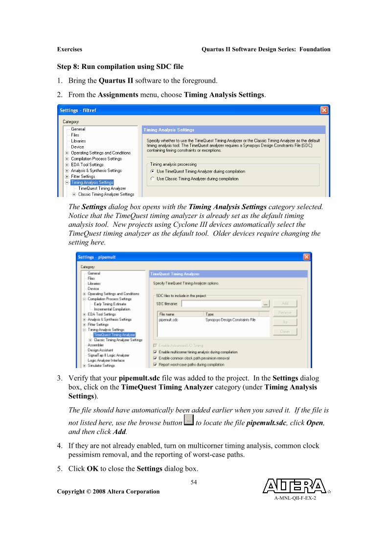
Step 8: Run compilation using SDC file
1. Bring the Quartus II software to the foreground.
2. From the Assignments menu, choose Timing Analysis Settings.
The Settings dialog box opens with the Timing Analysis Settings category selected.
Notice that the TimeQuest timing analyzer is already set as the default timing
analysis tool. New projects using Cyclone III devices automatically select the
TimeQuest timing analyzer as the default tool. Older devices require changing the
setting here.
3. Verify that your pipemult.sdc file was added to the project. In the Settings dialog
box, click on the TimeQuest Timing Analyzer category (under Timing Analysis
Settings).
The file should have automatically been added earlier when you saved it. If the file is
not listed here, use the browse button to locate the file pipemult.sdc, click Open,
and then click Add.
4. If they are not already enabled, turn on multicorner timing analysis, common clock
pessimism removal, and the reporting of worst-case paths.
5. Click OK to close the Settings dialog box.

Quartus II Software Design Series: Foundation Exercises
Copyright © 2008 Altera Corporation A-MNL-QII-F-EX-2
55
6. Click on or select Start Compilation from the Processing menu or Compile
Design from the Tasks window.
7. When compilation is complete, open the TimeQuest Timing Analyzer folder in the
Compilation Report.
Are you meeting or missing timing? A quick glance of the summary reports for each
of the three timing models will tell you. Make sure to check the fast, slow, and slow
0°C models. Are any shown in red? If not, then your timing has been validated. You
do not need to check any further.
8. Record the worst setup and hold slack in Table 3 (beginning of exercise).
Remember that the worst setup or hold slack could be either in any of the three
models. You can get this information from the Multicorner Timing Analysis
Summary report, but this report doesn’t indicate which model produced the worst-
case slack.
Exercise Summary
• Practiced basic steps for using TimeQuest
• Entered SDC timing constraints for analysis
END OF EXERCISE 5

Exercises Quartus II Software Design Series: Foundation
Copyright © 2008 Altera Corporation A-MNL-QII-F-EX-2
56
Exercise 6

Quartus II Software Design Series: Foundation Exercises
Copyright © 2008 Altera Corporation A-MNL-QII-F-EX-2
57
Exercise 6
Objectives:
• Create a chain description file (CDF) to use in programming a JTAG chain
• Use Programmer tool to configure a device
Step 1 (Connect Development Board & Open Quartus II Project)
1. Take out your development board. Connect the USB cable.
2. Open the project top_counter.qpf located in the Ex5 directory.
3. Compile the project.
This project contains a simple 2-digit decimal counter.
Step 2 (Open and Set Up Programmer to Configure Device)
1. From the Tools menu, select Programmer (or click on the or the toolbar
button).
This will open a CDF file. The CDF file lists all of the devices in your configuration
or JTAG chain along any associated programming or configuration files.
2. Save the CDF file. Use the default name.
3. Locate the Hardware Setup button at the top of the CDF file. The field to the right
of this button should read the USB-Blaster cables.
If this window reads anything else, click on the Hardware Setup button and locate
USB-Blaster cables min the drop-down menu of Currently selected hardware. Click
Close.
4. Back in the CDF file, use the drop-down Mode field to choose JTAG, if not already
selected.
5. In the main programming window, you should see the counter_<device>.sof
(configuration) file listed along with its target device.
If you do not see the counter_<device>.sof configuration file listed in the
programmer window, click on the Add File button and select it.

Exercises Quartus II Software Design Series: Foundation
Copyright © 2008 Altera Corporation A-MNL-QII-F-EX-2
58
6. Enable the Program/Configure option for the configuration file and target device as
shown above.
Remember if you want to bypass any devices in your JTAG chain, you can simply
leave this option unchecked for those devices.
7. Click on the Start button to begin configuration.
The LED display should begin counting from 0 to 99 when configuration is complete.
Exercise Summary
• Created a Chain Description File (CDF)
• Programmed an FPGA device
END OF EXERCISE 6