laboratory exercise #6 introduction to logic...
TRANSCRIPT

Laboratory Exercise #6Introduction to Logic Simulation and Verilog
ECEN 248: Introduction to Digital Design
Department of Electrical and Computer EngineeringTexas A&M University
2 Laboratory Exercise #6
1 Introduction
In the previous labs, we tested and debugged our digital designs by bread-boarding the actual circuits usingICs. For small designs, this method proved to be quite effective, and in the late 1960’s and early 1970’s,this was standard practice. However, as the gate counts of our circuits increased, this method became farless attractive. Thankfully, with advances in computer technology, there are alternatives to bread-boardingcircuits. In this day and age, we can effectively simulate the operation of our digital circuits during thedesign process without being burdened with the tedium you all have experienced up to this point. In lab thisweek, we will demonstrate the concept of digital circuit simulation and, in doing so, introduce Verilog R©
HDL, an Institute of Electrical and Electronics Engineers (IEEE) standard Hardware Description Language(HDL).
2 Background
The following subsections will provide you with some of the background necessary to understand and ap-preciate the way modern digital design is carried out. For a more in-depth treatment, please consult thecourse text book.
2.1 Verilog HDL
Programming languages have proven to be effective for software development. Interestingly, a similar truthholds for hardware development. Just as programming languages boost developer productivity, HardwareDescription Languages (HDLs) do so through various levels of abstraction, while providing a means to suc-cinctly describe digital circuits. What differentiates a traditional programming language from a standardHDL is the manner in which operations described within the language are handled. In a tradition program-ming language such as C, operations happen sequentially, and conditional statements facilitate changes inprogram flow. In contrast, the operations described in an HDL happen concurrently, and signals (often callednets) allow concurrent operations to interact with one another.
In the 1980’s, two competing HDLs were developed, namely VHDL and Verilog. Today, both languagesco-exist, encouraging tool vendors to support VHDL and Verilog simultaneously within a single design. Forour work in this lab, we will concentrate on Verilog; however, it is important to note that many of theHDL principals demonstrated here apply to VHDL as well. Verilog offers various levels of abstraction fordescribing digital circuits with structural at the bottom and behavioral at the top. Any given design couldhave a mixture of these abstraction levels, but in this lab assignment, we will start at the lowest level andmove up. The example shown below uses structural Verilog and the gate-level primitives built into Verilogto describe the 1-bit wide, 2:1 multiplexer you designed in the previous lab. The corresponding gate-level
2 ECEN 248

Laboratory Exercise #6 3
schematic in Figure 1 labels the module ports, internal wires, and gate instance names according to theprovided Verilog code.
Figure 1: Gate-level Schematic of a 1-bit wide, 2:1 MUX
1 ‘ t i m e s c a l e 1 ns / 1 ps‘ d e f a u l t n e t t y p e none
3 /∗ T h i s module d e s c r i b e s a 1− b i t wide m u l t i p l e x e r u s i n g s t r u c t u r a l c o n s t r u c t s ∗∗and gate− l e v e l p r i m i t i v e s b u i l t i n t o V e r i l o g . ∗ /
5module two one mux (Y, A, B , S ) ; / / d e f i n e t h e module name and i t s i n t e r f a c e
7/∗ d e c l a r e o u t p u t and i n p u t p o r t s ∗ /
9 output wire Y; / / d e c l a r e o u t p u t o f t y p e wi reinput wire A, B , S ; / / d e c l a r e i n p u t s o f t y p e wi re
11/∗ d e c l a r e i n t e r n a l n e t s ∗ /
13 wire notS ; / / i n v e r s e o f Swire andA ; / / o u t p u t o f and0 g a t e
15 wire andB ; / / o u t p u t o f and1 g a t e
17 /∗ i n s t a n t i a t e ga te− l e v e l modules ∗ /not no t0 ( notS , S ) ;
19 and and0 ( andA , notS , A ) ;and and1 ( andB , S , B ) ;
21 or or0 (Y, andA , andB ) ;
23 endmodule / / d e s i g n a t e end o f module
Syntactically, Verilog is very similar to the C programming language. Comments are designated ina similar fashion (i.e. \∗ ∗/ for comments which span multiple lines or \\ for single line comments),and semicolons end declarations, assignments, and statements. Verilog is case-sensitive and all keywordsare lowercase. The keyword, module, marks the beginning of the Verilog module, while the keyword,
ECEN 248 3
4 Laboratory Exercise #6
endmodule, marks the end. In the example above, the module name is two one mux, and its ports are Y,A, B, and S. The port order is not enforced by the language but follows a common convention in which theoutput ports are first, followed by the input ports. The keyword, output, is used to declare a net as an outputport, while input declares a net as an input port. Nets can be of type wire or reg. For now, we will onlybe concerned with wires. Nets can take on one of four values, namely ‘1’, ‘0’, ‘Z’, and ‘X’ for high, low,floating, and undefined, respectively. Modules, whether built-in or user-defined, are instantiated as seen inlines 14 through 19 of the code above. The module name is followed by the instance name. The instancename must obviously be unique; however, multiple instances of the same module may exist. Notice theorder of ports for the built-in primitives (i.e. not, and, or) follows the convention discussed above such thatthe output port is first, followed by the input ports. Since these operations are associative, the order of theinputs is not important.
2.2 Xilinx ISE
Xilinx R© Integrated Software Environment (ISETM) version 13.4 is the hardware development tool that wewill be using in this laboratory. Xilinx manufacturers a wide variety of reprogrammable logic devices (wewill discuss these further in the next lab) and supplies ISE as a means to develop for these devices. Conse-quently, ISE is an excellent teaching tool for modern digital design. It supports digital circuit simulation,which is the focus of this week’s lab assignment, in addition to all of the implementation processes neces-sary to load a design into an Xilinx part. It comes with an easy-to-use Graphical User Interface (GUI) andwaveform viewer and supports both VHDL and Verilog. Xilinx ISE is part of a larger class of computer-aided design (CAD) tools used to develop digital circuits. For additional information on Xilinx and ISE13.4, consult the manufacturer’s website at: www.xilinx.com
2.3 Linux OS
Linux is an open-source Unix-like operating system (OS) commonly used in industry. The open-sourcelicense allows it to be used free of charge, which makes it a big win for the university setting. The Unixaspect allows Linux to be compatible with many of the CAD tools out on the market today. The Linuxkernel along with the various support packages makeup the specific Linux distribution. The machines in theECEN248 lab (Zach 115C) have a variant of Red Hat Linux called CentOS installed on them because manyof the tool vendors will provide support for only Red Hat Linux.
The CentOS Linux installation has a window manager, which gives you the look and feel similar to thatof MS Windows or MacOS. However, the Linux terminal is available for those acquainted with Unix. As aresult, you will be provided with commands to execute in the terminal throughout the lab session. Please tryto understand what these commands do so that you can execute them in future labs without instruction. Theformat of the commands provided is shown below. The command to be executed follows the > symbol.
>command argument0 argument1
4 ECEN 248

Laboratory Exercise #6 5
Note: Please ensure that you have a Unix account with the ECE department before arriving to your labsession. It is imperative that you are able to log into the CentOS machines in Zach 115C.
3 Pre-lab
We will reuse the designs created in Lab 3 and Lab 4 for this week’s lab so no pre-lab submission is required.However, you will be expected to have the appropriate material ready for lab so please read over the entirelab manual before coming to your lab session.
4 Lab Procedure
The lab experiments below will guide you through the development of a simple 4-bit ALU in Verilog usingthe ISE software suite. Each module that you create will be individually tested using the built-in digitalcircuit simulator, ISim, with test bench files that we provide to you.
4.1 Experiment 1
The objective of this lab experiment is to familiarize you with the ISE development environment. Pleasetake note of what it is you are doing as you will be expected to perform similar exercises on your own infuture experiments.
1. Launch ISE Project Navigator and create a new design project.
(a) Open a terminal window in the CentOS workstation by selecting Applications→ Accessories→ Terminal and type the following command and hit “Enter” to create a work directory:
>mkdir $HOME/ecen248
(b) Now execute the following command to run ISE:
>/softwares/setup/xilinx/ise-13.4
(c) Once ISE loads, select File→ New ProjectThe New Project Wizard will open as illustrated below. Type a Project Name (ex. lab6) and aProject Location (ex. /ecen248/lab1 in your home directory). Then chose HDL as the Top-LevelSource Type and click “Next.”
ECEN 248 5

6 Laboratory Exercise #6
(d) Next, the ‘Project Settings’ window appears (see screenshot below).Set the following project settings:
Evaluation Development Board: Spartan-3E Starter BoardSimulator: ISim (VHDL/Verilog)Preferred Language: Verilog
6 ECEN 248

Laboratory Exercise #6 7
(e) Hit “Next” to continue. A Project Summary window will appear. Examine the summary andclick “Finish” when done.
2. Create a Verilog source file which describes the 2:1 MUX in Figure 1.
(a) From within ISE, select File→ New to create a new file.
(b) A dialog box will appear as seen above. Select “Text File” and press “OK.”
(c) Type the Verilog code example found the in the Background section of this manual into the ISEtext editor window.Note: Do NOT copy and paste text from the PDF into the editor window. Symbols within thecode do not always copy properly and will cause syntax errors when you attempt to build theproject.
(d) Select File→ Save and save the file you just created as “two one mux.v” within your lab6 di-rectory.
3. Add the 2:1 MUX source file and test bench to the ISE project.
(a) Right-click on the Xilinx part number (xc3s500e-4fg320) within the Hierarchy window andselect “Add Source...” as shown in below.
ECEN 248 7

8 Laboratory Exercise #6
(b) In the file browser, navigate to the source file you just created and hit “Open.”
(c) A window will appear with Association and Library fields. Leave these settings as default andpress “OK” to continue.
(d) Ensure the source file you just added appears under the Xilinx part number in the Hierarchywindow.
(e) Open a new terminal window and copy the appropriate test bench file from the ECEN248 direc-tory into you lab6 directory with the following commands:
>cd $HOME/ecen248/lab6>cp /homes/faculty/shared/ECEN248/two_one_mux_tb.v .
The first command changes the current directory to your lab6 directory, while the second com-mand copies the 2:1 MUX test bench into the current directory. You could also perform thisoperation in a single command by replacing the ‘.’ at the end of the copy command with thepath to your lab6 directory.
8 ECEN 248

Laboratory Exercise #6 9
(f) Add the “two one mux tb.v” file to your ISE project, leaving the source file properties as defaultagain.
(g) Change the “View” setting within the Hierarchy window to “Simulation” and ensure the hierar-chy appears as seen in below.
(h) Open the 2:1 MUX test bench file and take a moment to examine the contents. The test benchutilizes advanced concepts in Verilog that we have not discussed yet, but some things shouldlook familiar. A test bench file is nothing more than a Verilog module which instantiates theUnit Under Test (UUT) and stimulates the inputs for testing. Notice that the test bench moduledoes not have any ports of its own. The input and output ports of the UUT are what are important,and when we simulate the test bench file, we will examine those signals.
4. Simulate the 2:1 MUX test bench.
(a) Click on the ‘+’ symbol to the left of “ISim Simulator” in the Process window.
(b) Select the 2:1 MUX test bench file in the hierarchy window and then double click “SimulateBehavioral Model” from within the Process window.
ECEN 248 9

10 Laboratory Exercise #6
(c) If there are any errors or warnings, they will show up in the Console window. Correct any errorsand warnings at this time. You may re-run the simulation process once you have fixed yoursource code.
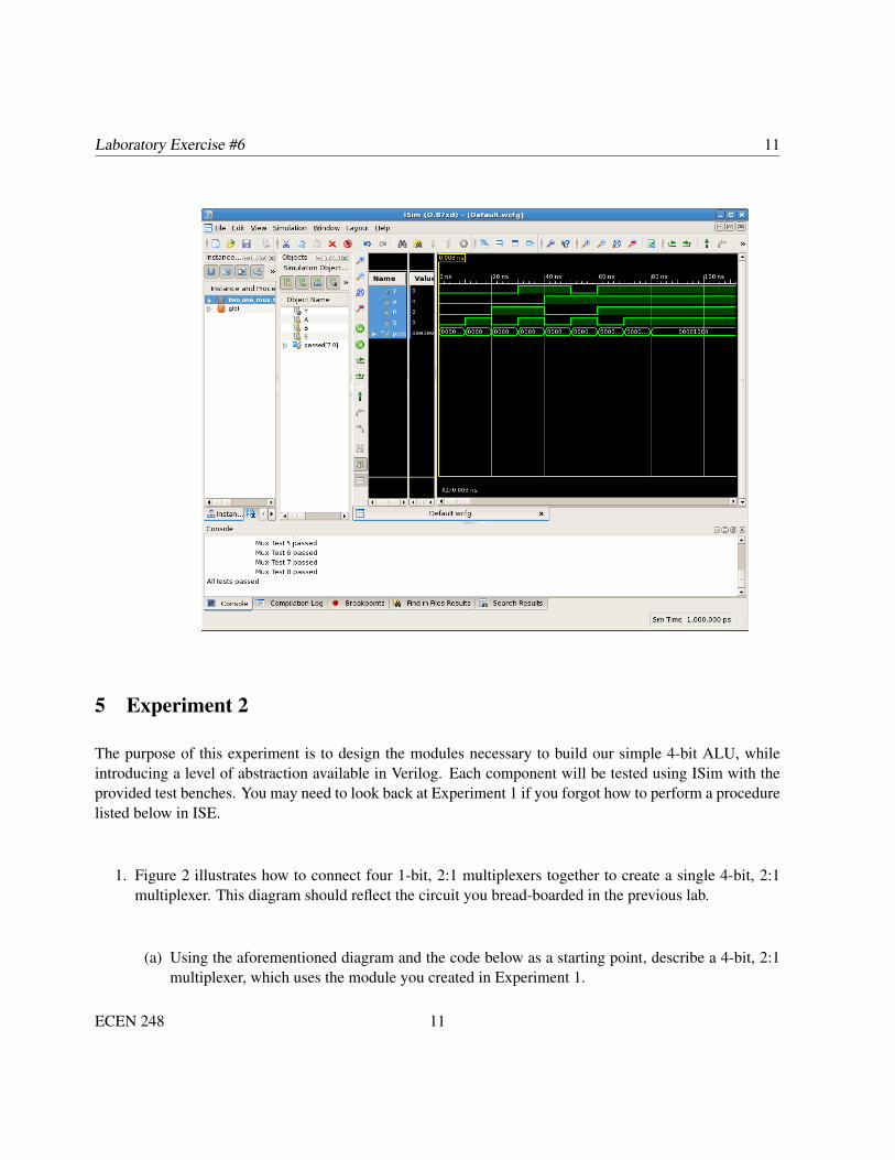
(d) The ISim window shown below will open once your design successfully compiles. Take note ofthe waveform window in the top-right corner and the Console window at the bottom. Notice thatthe test bench exercises the multiplexer through all of the possible input combinations. Ensurethat your design passes all of these tests. Please include a screenshot of the waveform in you labwrite-up along with the console output of the test bench.
10 ECEN 248
Laboratory Exercise #6 11
5 Experiment 2
The purpose of this experiment is to design the modules necessary to build our simple 4-bit ALU, whileintroducing a level of abstraction available in Verilog. Each component will be tested using ISim with theprovided test benches. You may need to look back at Experiment 1 if you forgot how to perform a procedurelisted below in ISE.
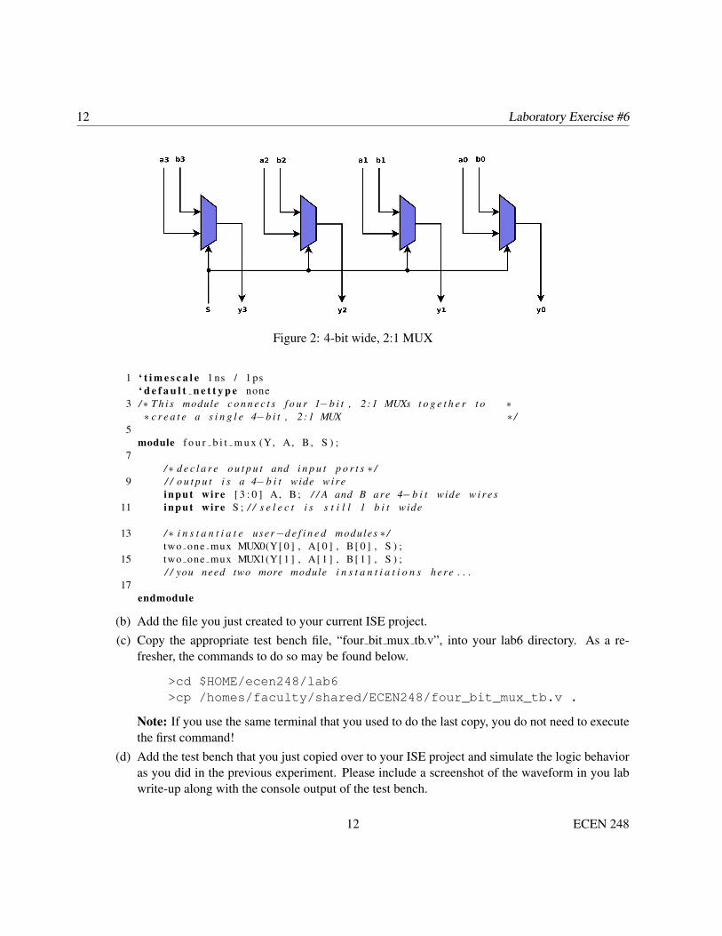
1. Figure 2 illustrates how to connect four 1-bit, 2:1 multiplexers together to create a single 4-bit, 2:1multiplexer. This diagram should reflect the circuit you bread-boarded in the previous lab.
(a) Using the aforementioned diagram and the code below as a starting point, describe a 4-bit, 2:1multiplexer, which uses the module you created in Experiment 1.
ECEN 248 11
12 Laboratory Exercise #6
Figure 2: 4-bit wide, 2:1 MUX
1 ‘ t i m e s c a l e 1 ns / 1 ps‘ d e f a u l t n e t t y p e none
3 /∗ T h i s module c o n n e c t s f o u r 1−b i t , 2 :1 MUXs t o g e t h e r t o ∗∗ c r e a t e a s i n g l e 4−b i t , 2 :1 MUX ∗ /
5module f o u r b i t m u x (Y, A, B , S ) ;
7/∗ d e c l a r e o u t p u t and i n p u t p o r t s ∗ /
9 / / o u t p u t i s a 4− b i t wide wi reinput wire [ 3 : 0 ] A, B ; / / A and B are 4− b i t wide w i r e s
11 input wire S ; / / s e l e c t i s s t i l l 1 b i t wide
13 /∗ i n s t a n t i a t e user−d e f i n e d modules ∗ /two one mux MUX0(Y[ 0 ] , A[ 0 ] , B [ 0 ] , S ) ;
15 two one mux MUX1(Y[ 1 ] , A[ 1 ] , B [ 1 ] , S ) ;/ / you need two more module i n s t a n t i a t i o n s here . . .
17endmodule
(b) Add the file you just created to your current ISE project.(c) Copy the appropriate test bench file, “four bit mux tb.v”, into your lab6 directory. As a re-
fresher, the commands to do so may be found below.
>cd $HOME/ecen248/lab6>cp /homes/faculty/shared/ECEN248/four_bit_mux_tb.v .
Note: If you use the same terminal that you used to do the last copy, you do not need to executethe first command!
(d) Add the test bench that you just copied over to your ISE project and simulate the logic behavioras you did in the previous experiment. Please include a screenshot of the waveform in you labwrite-up along with the console output of the test bench.
12 ECEN 248
Laboratory Exercise #6 13
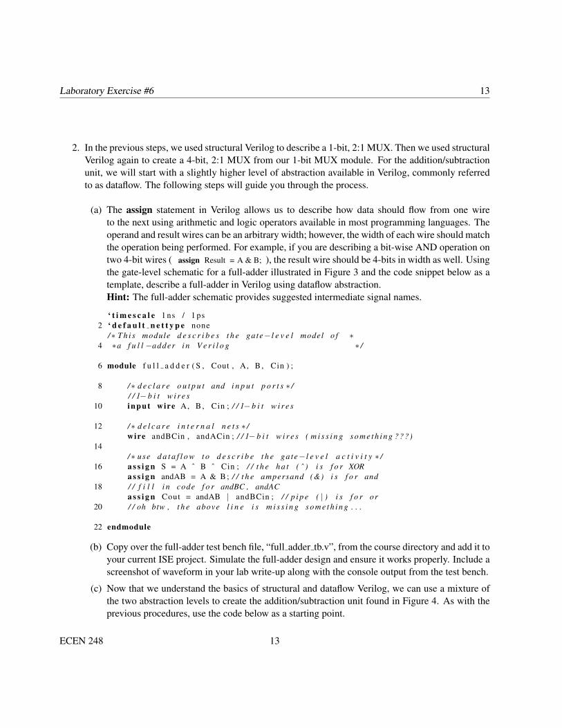
2. In the previous steps, we used structural Verilog to describe a 1-bit, 2:1 MUX. Then we used structuralVerilog again to create a 4-bit, 2:1 MUX from our 1-bit MUX module. For the addition/subtractionunit, we will start with a slightly higher level of abstraction available in Verilog, commonly referredto as dataflow. The following steps will guide you through the process.
(a) The assign statement in Verilog allows us to describe how data should flow from one wireto the next using arithmetic and logic operators available in most programming languages. Theoperand and result wires can be an arbitrary width; however, the width of each wire should matchthe operation being performed. For example, if you are describing a bit-wise AND operation ontwo 4-bit wires ( assign Result = A & B; ), the result wire should be 4-bits in width as well. Usingthe gate-level schematic for a full-adder illustrated in Figure 3 and the code snippet below as atemplate, describe a full-adder in Verilog using dataflow abstraction.Hint: The full-adder schematic provides suggested intermediate signal names.
‘ t i m e s c a l e 1 ns / 1 ps2 ‘ d e f a u l t n e t t y p e none
/∗ T h i s module d e s c r i b e s t h e gate− l e v e l model o f ∗4 ∗a f u l l −adder i n V e r i l o g ∗ /
6 module f u l l a d d e r ( S , Cout , A, B , Cin ) ;
8 /∗ d e c l a r e o u t p u t and i n p u t p o r t s ∗ // / 1− b i t w i r e s
10 input wire A, B , Cin ; / / 1− b i t w i r e s
12 /∗ d e l c a r e i n t e r n a l n e t s ∗ /wire andBCin , andACin ; / / 1− b i t w i r e s ( m i s s i n g s o m e t h i n g ???)
14/∗ use d a t a f l o w t o d e s c r i b e t h e gate− l e v e l a c t i v i t y ∗ /
16 a s s i g n S = A ˆ B ˆ Cin ; / / t h e h a t ( ˆ ) i s f o r XORa s s i g n andAB = A & B ; / / t h e ampersand (&) i s f o r and
18 / / f i l l i n code f o r andBC , andACa s s i g n Cout = andAB | andBCin ; / / p i p e ( | ) i s f o r or
20 / / oh btw , t h e above l i n e i s m i s s i n g s o m e t h i n g . . .
22 endmodule
(b) Copy over the full-adder test bench file, “full adder tb.v”, from the course directory and add it toyour current ISE project. Simulate the full-adder design and ensure it works properly. Include ascreenshot of waveform in your lab write-up along with the console output from the test bench.
(c) Now that we understand the basics of structural and dataflow Verilog, we can use a mixture ofthe two abstraction levels to create the addition/subtraction unit found in Figure 4. As with theprevious procedures, use the code below as a starting point.
ECEN 248 13

14 Laboratory Exercise #6
Figure 3: Full-Adder Gate-level Schematic
Figure 4: Addition/Subtraction Unit
1 ‘ t i m e s c a l e 1 ns / 1 ps‘ d e f a u l t n e t t y p e none
3 /∗ T h i s V e r i l o g module d e s c r i b e s a 4− b i t a d d i t i o n / s u b t r a c t i o n ∗∗ u n i t u s i n g f u l l −adder modules which have a l r e a d y been ∗
5 ∗ d e s i g n e d and t e s t e d . ∗ /
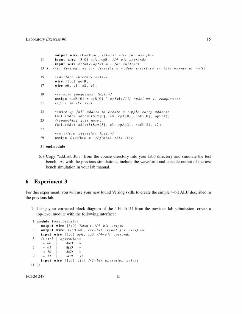
7 module a d d s u b (/∗ d e c l a r e o u t p u t and i n p u t p o r t s ∗ /
9 output wire [ 3 : 0 ] Sum , / / 4− b i t r e s u l t
14 ECEN 248
Laboratory Exercise #6 15
output wire Overflow , / / 1− b i t w i r e f o r o v e r f l o w11 input wire [ 3 : 0 ] opA , opB , / / 4− b i t operands
input wire opSe l / / o p S e l = 1 f o r s u b t r a c t13 ) ; / / i n V e r i l o g , we can d e s c r i b e a module i n t e r f a c e i n t h i s manner as w e l l !
15 /∗ d e c l a r e i n t e r n a l n e t s ∗ /wire [ 3 : 0 ] notB ;
17 wire c0 , c1 , c2 , c3 ;
19 /∗ c r e a t e complement l o g i c ∗ /a s s i g n notB [ 0 ] = opB [ 0 ] ˆ opSe l ; / / i f o p S e l == 1 , complement
21 / / f i l l i n t h e r e s t . . .
23 /∗ wire up f u l l a dde r s t o c r e a t e a r i p p l e c a r r y adder ∗ /f u l l a d d e r a dd e r0 (Sum [ 0 ] , c0 , opA [ 0 ] , notB [ 0 ] , opSe l ) ;
25 / / s o m e t h i n g goes here . . .f u l l a d d e r a dd e r3 (Sum [ 3 ] , c3 , opA [ 3 ] , notB [ 3 ] , c2 ) ;
27/∗ o v e r f l o w d e t e c t i o n l o g i c ∗ /
29 a s s i g n Overf low = ; / / f i n i s h t h i s l i n e
31 endmodule
(d) Copy “add sub tb.v” from the course directory into your lab6 directory and simulate the testbench. As with the previous simulations, include the waveform and console output of the testbench simulation in your lab manual.
6 Experiment 3
For this experiment, you will use your new found Verilog skills to create the simple 4-bit ALU described inthe previous lab.
1. Using your corrected block diagram of the 4-bit ALU from the previous lab submission, create atop-level module with the following interface:
1 module f o u r b i t a l u (output wire [ 3 : 0 ] R e s u l t , / / 4− b i t o u t p u t
3 output wire Overflow , / / 1− b i t s i g n a l f o r o v e r f l o winput wire [ 3 : 0 ] opA , opB , / / 4− b i t operands
5 /∗ c t r l | o p e r a t i o n ∗∗ 00 | AND ∗
7 ∗ 01 | ADD ∗∗ 10 | AND ∗
9 ∗ 11 | SUB ∗ /input wire [ 1 : 0 ] c t r l / / 2− b i t o p e r a t i o n s e l e c t
11 ) ;
ECEN 248 15
16 Laboratory Exercise #6
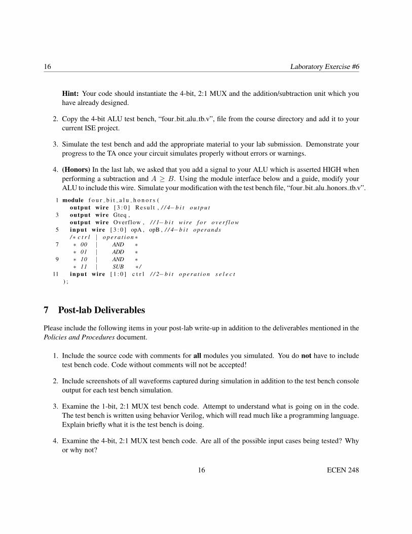
Hint: Your code should instantiate the 4-bit, 2:1 MUX and the addition/subtraction unit which youhave already designed.
2. Copy the 4-bit ALU test bench, “four bit alu tb.v”, file from the course directory and add it to yourcurrent ISE project.
3. Simulate the test bench and add the appropriate material to your lab submission. Demonstrate yourprogress to the TA once your circuit simulates properly without errors or warnings.
4. (Honors) In the last lab, we asked that you add a signal to your ALU which is asserted HIGH whenperforming a subtraction and A ≥ B. Using the module interface below and a guide, modify yourALU to include this wire. Simulate your modification with the test bench file, “four bit alu honors tb.v”.
1 module f o u r b i t a l u h o n o r s (output wire [ 3 : 0 ] R e s u l t , / / 4− b i t o u t p u t
3 output wire Gteq ,output wire Overflow , / / 1− b i t w i r e f o r o v e r f l o w
5 input wire [ 3 : 0 ] opA , opB , / / 4− b i t operands/∗ c t r l | o p e r a t i o n ∗
7 ∗ 00 | AND ∗∗ 01 | ADD ∗
9 ∗ 10 | AND ∗∗ 11 | SUB ∗ /
11 input wire [ 1 : 0 ] c t r l / / 2− b i t o p e r a t i o n s e l e c t) ;
7 Post-lab Deliverables
Please include the following items in your post-lab write-up in addition to the deliverables mentioned in thePolicies and Procedures document.
1. Include the source code with comments for all modules you simulated. You do not have to includetest bench code. Code without comments will not be accepted!
2. Include screenshots of all waveforms captured during simulation in addition to the test bench consoleoutput for each test bench simulation.
3. Examine the 1-bit, 2:1 MUX test bench code. Attempt to understand what is going on in the code.The test bench is written using behavior Verilog, which will read much like a programming language.Explain briefly what it is the test bench is doing.
4. Examine the 4-bit, 2:1 MUX test bench code. Are all of the possible input cases being tested? Whyor why not?
16 ECEN 248

Laboratory Exercise #6 17
5. In this lab, we approached circuit design in a different way compared to previous labs. Compare andcontrast bread-boarding techniques with circuit simulation. Discuss the advantages and disadvantagesof both. Which do you prefer? Similarly, provide some insight as to why HDLs might be preferredover schematics for circuit representation. Are there any disadvantages to describing a circuit usingan HDL compared to a schematic? Again, which would you prefer.
6. Two different levels of abstraction were introduced in this lab, namely structural and dataflow. Providea comparison of these approaches. When might you use one over the other?
7. (Honors) Examine the 4-bit ALU test bench code. The test bench actual computes the result it isexpecting from the hardware that it is testing and uses this result to perform a known answer com-parison. Notice that Overflow detection is done slightly different in the test bench. How is overflowdetection different in the test bench compared to the UUT? Similarly, how is the result computationdifferent?
8 Important Student Feedback
The last part of lab requests your feedback. We are continually trying to improve the laboratory exercisesto enhance your learning experience, and we are unable to do so without your feedback. Please include thefollowing post-lab deliverables in your lab write-up.
Note: If you have any other comments regarding the lab that you wish to bring to your instructor’s attention,please feel free to include them as well.
1. What did you like most about the lab assignment and why? What did you like least about it and why?
2. Were there any section of the lab manual that were unclear? If so, what was unclear? Do you haveany suggestions for improving the clarity?
3. What suggestions do you have to improve the overall lab assignment?
ECEN 248 17