lab_on_chip; opportunity for chemical engineering
DESCRIPTION
paperTRANSCRIPT
Introduction
Lab-on-a-chip is becoming an increasingly familiar termused to connote the miniaturization of chemical, biologicaland biochemical analyses. In a broad functional sense, a
lab-on-a-chip system for most (commercial) applications consistsof a microchip, an instrument for control and detection, a comput-er with control and data analysis software, and assays and reagents.The key concept is integration and the thinking is guided by a sys-tem’s viewpoint.
In one respect, a lab-on-a-chip system can be viewed as a scaled-down analog of a chemical processing plant because many processfunctions are similar. Undoubtedly, one key benefit in miniaturiza-tion is the drastic reduction of reagent consumption, which trans-lates to cost savings in many applications. There are, however, twoother important benefits that may be less obvious: integration andautomation. Integration of multiple processes or functions in a sin-gle platform offers the advantages of faster analysis and sometimesnovel, synergistic capabilities that may not be attainable otherwise.Automation allows more precise and reproducible operations result-ing in higher data quality. All three benefits combined enable high-throughput, high quality experimentation of complex processes.
The initial concept of lab-on-a-chip, or “miniaturized totalchemical analysis system,” has been accredited to Manz et al.(1990), who proposed the use of integrated microfabricateddevices for sample pretreatment, separation, and detection forchemical analysis. Reports of the early 1990s are often cited aspioneer studies that ignited the research in this field, but Terrydemonstrated a microfabricated silicon gas chromatographic ana-lyzer in 1975, which received very little attention from the scien-tific community. [For detailed history and early literature, see arecent review article by Reyes et al. (2002).] Since then, the fieldhas been growing at a rapid pace, as indicated by numerous pub-lications and citations, as well as the number of conferencesfocused on this new field.
Commercial development of lab-on-a-chip applications startedin the mid-1990s by an infusion of venture capital funds, whichsupported the startup of many microfluidics companies. In 1999,the first lab-on-a-chip commercial product was introduced basedon a collaboration between Caliper Technologies Corp. and AgilentTechnologies (see http://www.chem.agilent.com/Scripts/PCol.asp?lPage=50 for details of the Agilent 2100 bioanalyzer prod-ucts). In 2001, a journal called Lab on a Chip: Miniturisation ofChemistry and Biology was launched by the Royal Society ofChemistry to cover the growing field of research and technology
development (see http://www.rsc.org/is/journals/current/loc/locpub.htm). By all early indications and the amount of currentwork, the lab-on-a-chip concept seems exciting and extremelyviable for many applications. This technology may revolutionizethe way laboratory manipulations are performed, the basic formatof which has not changed significantly over the past 100 years.
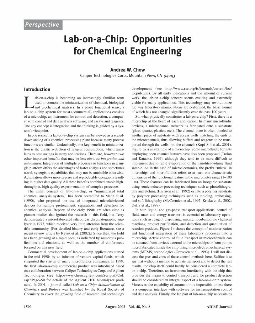
So, what physically constitutes a lab-on-a-chip? First, there is amicrochip at the heart of each application. In many microfluidicdevices, a microchannel network is fabricated onto a substrate(glass, quartz, plastics, etc.). The channel plate is often bonded toanother piece of substrate with access wells matching the ends ofthe microchannels, thus allowing buffers and reagents to be trans-ported through the wells into the channels (Kopf-Sill et al., 2001).Figure 1a is an example of a microchip. Some microfluidic formatsemploying open channel features have also been proposed (Troianand Kataoka, 1999), although they tend to be more difficult toimplement due to rapid evaporation of the nanoliter-volume fluidsample. As in the case of microelectronics, the prefix “micro” inmicrochips and microfluidics refers to at least one characteristicdimension of the functional feature in the micrometer range (1–100µm). These features can be fabricated into an inorganic substrateusing semiconductor processing techniques such as photolithogra-phy and etching (Harrison et al., 1992) or into a polymer substrateby polymer processing techniques such as molding, embossing,and soft lithography (McCormick et al., 1997; Kricka et al., 2002;Duffy et al., 1998).
In both liquid- and gas-phase transport applications, control offluid, mass and energy transport is essential to laboratory opera-tions such as reagent dispensing, mixing, incubation for chemicalreactions, product purification, and detection and quantitation ofreaction products. Figure 1b shows the concept of miniaturizationand functional integration of these laboratory processes onto amicrochip. Active control of fluid transport in microchannels canbe actuated from devices external to the microchips or from pumpsmicrofabricated inside the chip using microelectromechanical sys-tems (MEMS) technologies (Gravesen et al., 1993). I will not dis-cuss the pros and cons of these control methods here. Suffice it tosay that without a method to actuate transport and to detect the testresults, the chip itself could hardly be considered a complete lab-on-a-chip. Therefore, an instrument interfacing with the chip thatprovides the means to control transport and for product detectionshould be considered an integral aspect of a lab-on-a-chip system.Moreover, the capability of automation is impossible unless thereis a computer interface with software for instrumentation controland data analysis. Finally, the lab part of lab-on-a chip necessitates
Lab-on-a-Chip: Opportunities
for Chemical Engineering
Andrea W. ChowCaliper Technologies Corp., Mountain View, CA 94043
PPeerrssppeeccttiivvee
1590 August 2002 Vol. 48, No. 8 AIChE Journal
a reagent or assay component. Thus, in a broad functional sense, alab-on-a-chip system for most (commercial) applications consistsof the four physical components-a microchip, an instrument forcontrol and detection, a computer with control and data analysissoftware, and assays and reagents.
Scientific and Research Challenges
Two recent articles fea-tured in AIChE Journal’sPerspective column de-scribe the benefits andresearch challenges ofsome key lab-on-a-chipfunctions. Jensen (1999)addresses the area ofmicroreactors or micro-chemical systems. Im-proved thermal man-agement, controlled reac-tant distribution, and fastmass-transfer rates arecited as some of the advan-tages of these microreac-tors. The real value ofminiaturization lies in theexploration of new reac-tion pathways and findingalternative solutions tochemical manufacturing.Stone and Kim (2001) dis-cuss the scientific chal-lenges of microfluidics.Fluid and mass transportissues including Taylor-Aris dispersion, flow-field-fractionation for sep-aration processes, mixingin laminar flow, flow ofconfined polymers, andmultiphase transport arecited as current activeareas of research.
Other reviews suggestthe importance of inte-grating other lab-on-a-chip functions includingon-chip sample prepara-tion and purification,novel physical and chem-ical affinity separationprocesses, and interfacingmicrochips with detectionmethods such as massspectrometry (Sanders and Manz, 2000; de Mello, 2001). Controlof surface chemistry and interfacial interactions on channel wallsis another important aspect for many applications (Mrksich andWhitesides, 1995; Zhao et al., 2001). The importance of on-chipintegration of flow actuators and sensors for lab-on-a-chip deviceshas also been emphasized (Gravesen et al., 1993; Unger et al.,
2000). Furthermore, the development of polymeric devices to takeadvantage of polymer processing methods for fast prototyping andmass production of low cost lab-on-a-chip applications hasreceived a lot of attention (Effenhauser et al., 1997; McCormick etal., 1997; Duffy et al., 1998).
Undoubtedly, the development of lab-on-a-chip applications istremendously multidisciplinary, with research and engineering
opportunities straddlingacross chemical engi-neering, biology, chem-istry, physics, materials,processing science, sur-face science, informationscience, and other engi-neering disciplines. Withso many outstandingtechnological challenges,where does one begin toadvance the lab-on-a-chip concept from R&Dto commercialization?
Application and
Product Develop-
ment Challenges
In developing anycommercial applicationor product, one needs tounderstand clearly twoissues:
(1) What are the spe-cific features that makethe product an interestingand competitive offering(does it have the featuresneeded to do the job)?
(2) Why would peo-ple want to buy this prod-uct (is it an affordablesolution to a real need)?
The answers to thesequestions help define thefunctional specificationsof the product. For a spe-cific lab-on-a-chip appli-cation, the overall sys-tem specifications, aswell as the flow-downspecifications for each ofthe four components(chip, instrument, soft-ware, and reagents), need
to be defined specifically for that product. Functional integration ofsubcomponents in the microchip and system integration of all fourcomponents are the key challenges in developing this technologyinto viable commercial products. This point will be explainedusing a specific example of high-throughput screening for drugdiscovery, based on Caliper’s technology.
AIChE Journal August 2002 Vol. 48, No. 8 1591
Figure 1. (a) Microfluidic microchip fabricated in glass; (b) miniaturizing
and integrating laboratory processes onto a microchip device.
(a)
(b)
In developing a successful drug to treat a specific disease, one ofthe first steps used by pharmaceutical companies is to screen alarge library of compounds to identify lead compounds for furtherdevelopment (Sittampalam et al., 1997). In this initial phase of thedrug development process, tens of thousands to over a millioncompounds are routinely tested against a “target,” usually a bio-molecule such as an enzyme or a receptor on a cell membrane sur-face that has been identi-fied as playing an impor-tant role in controlling thedisease. Currently, thestandard format is amicrotiter plate for stor-ing the compounds andperforming the assays.These plastic plates areabout 5 in. × 3 in. in sizeand contain an array ofwells numbering from 48to 1,536, with the mostcommonly used onesbeing 96- and 384-wellformats. Most high-throughput screeningfacilities are equippedwith laboratories full ofrobots and automationequipment to handlethese plates, moving themfrom station to station forreagent dispensing, mix-ing, reaction incubationand readout of the assayresults mostly based onfluorescence or radiomet-ric detection methods.
System design and
integration
High-throughput screen-ing can benefit readilyfrom the miniaturization,integration, and automa-tion offered by lab-on-a-chip technologies. Indeveloping such a product,one system considerationis deciding how to parti-tion disposable and non-disposable components.Some researchers in thefield propose integratingmany functions, includingmicropumps for flow actu-ation and detection mi-crosensors, onto the chip itself as the ultimate goal of integration forlab-on-a-chip applications. However, from the economics perspective,the chip may become too expensive to manufacture if it is considereddisposable or semidisposable (e.g., a single chip is used for up to a day
for running tens of thousands of experiments.) Consequently, one rea-sonable choice is to have passive channels on a chip, with flow actu-ation mechanism and detection optics incorporated in the instrument,which is not disposable and can be less cost-sensitive.
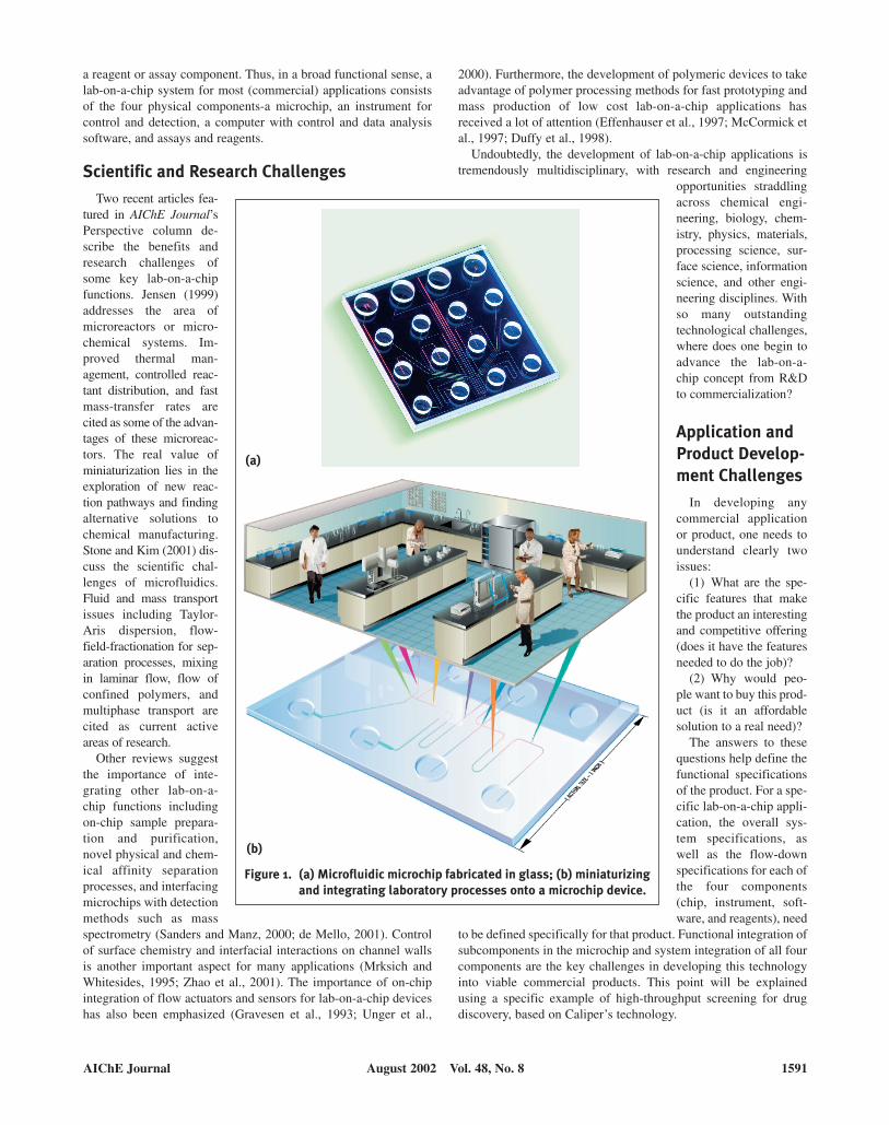
Devising a lab-on-a-chip system for high-throughput screeningrequires developing a suitable world-to-chip interface capable ofautomating compound sampling from the microtiter plate format.
This interface, integratingthe chip to the existingsample storage, must bemanufacturable, have lowdead volume such thatsample cross-contamina-tion is minimized, and bescaleable to increasethroughput via parallelprocessing. One solutionis a sipper chip formatthat uses a capillary con-nection to allow the pla-nar microchannel net-work to communicate flu-idically to the outsideworld. A few nanoliters ofeach compound in solu-tion can be brought ontothe chip serially, and adja-cent compounds are sepa-rated by a buffer spacer tokeep the samples spatiallydistinct. Figure 2a illus-trates the concept of seri-al compound accession,and Figure 2b shows thesipper chip family, from 1to 12 sipper connectionsin one single chip.
Functional integra-
tion on chip
One level down fromthe overall system, thedetailed functional specifi-cations for chip design aredetermined by the specificassays to be performed inthe chip. The number ofquestions may surprise thenonexperts. The followingis a list of the questions weneed to answer for eachassay type:
• What are the charac-teristics of the reagents andproducts for the assay?
• How should the fluids and reagents from the sipper and in themicrochannels be transported?
• In what order must the reagents be added and what are themixing requirements?
1592 August 2002 Vol. 48, No. 8 AIChE Journal
Figure 2. (a) Automated compound sampling through a sipper capillary
into a microchip device with blue sample plugs separated by
clear buffer spacers as they are brought onto the chip serially;
(b) sipper chip family including 1-, 4- and 12-sipper chips.
(a)
(b)

• What is the chemistry or biochemistry involved in the reac-tion? How long does the reaction mixture need to incubate and atwhat temperature? What are the design criteria for the reactor?
• Do the products need to be separated from the reactants beforedetection? If yes, what separation method should be used and whatare the optimal conditions?
• What are the mass and volumetric flow rates in and out of thevarious unit operations in the chip? Is the yield of products highenough to meet detection requirements?
• How much heat is generated or required in each unit operationand what method should be used to manage the heat flow in and outof the chip?
• For each unit operation, is it continuous flow or batch process?If mixed mode processes are used, how do we integrate the differ-ent processes?
• What are the key scaling parameters in the design? How do wetake bench top results and scale it down for microfluidic processing?
• When all the necessary unit operations are integrated togetheron chip, what is the overall sample throughput? Does it still makea viable product?
These issues are similar to the ones that would be asked in thebeginning of a more conventional chemical process plant designproject. It is then apparent that answering these questions most def-initely needs the analytical skills in mass and energy balance,transport phenomena, reaction kinetics, separation processes,dimensional analysis and scaling laws, unit operations, processcontrol, economic analysis, and other subjects found in most chem-ical engineering curriculum.
To complete my example on functional integration on chip, Iwill use kinase enzymatic assays for high throughput screening toillustrate the development process. Kinases are an important classof enzymes that the body uses to regulate many biochemical path-ways and are, therefore, very interesting pharmaceutical targets.Functionally, a kinase takes a phosphate group from adenosinetriphosphate (ATP) and puts it onto a peptide (called “substrate”)containing a specific sequence of amino acids that the kinase rec-ognizes, thereby turning it into a product that is more negativelycharged (this process is called “phosphorylation”). A kinasescreening assay is relatively difficult to run on the conventionalmicrotiter plate format, because no one has yet been able to find away to make the assay “fluorogenic,” meaning that the fluores-cence signal of the labeled substrate changes as it turns into a prod-uct. Without a changing fluorescence signal, one must separate theproduct from the substrate before detecting the extent of reaction.This requires chemically or physically stopping the reaction, thenusing a separation means (such as a chromatographic column) todifferentiate the product from the substrate, and then measure theproduct or substrate concentration. In a high-throughput environ-ment in traditional formats, these steps are difficult to implement.
To develop a microfluidic kinase assay for screening, we can takeadvantage of the fact that the substrate and product have differentelectrophoretic mobilities because the product is more negativelycharged than the substrate. Following reaction incubation, an elec-trophoretic separation step can be used to quantify the rate of reac-tion by comparing the ratio of the substrate to product signal. We canuse the approach of inject-and-separate using a channel intersectionas a virtual valve that many have demonstrated on chip, in which analiquot of reaction mixture can be injected into a separation channelusing an injection scheme such as pinched injection or gated injec-tion (Jacobson et al, 1994). Under adequate electric field strength
and separation time, the resulting signal shows two separate peaksbecause the two labeled species travel at different velocities underthe applied field. However, inject-and-separate is inherently a batchprocess, which makes integrating it into the continuous flow reactionincubation step more difficult. At the very least, one would need tomonitor when each sample reaction mixture arrives at the injectionintersection to time the sample injection into the separation channel.
To avoid the complexity of timing of injections, we consider thealternative of turning the separation process from batch to contin-uous flow. In this case, we use the injection of sample into the sip-per as the injection step for the reaction, as well as for the separa-tion. The potential drawback is that the sample plug injectedthrough the sipper is usually much larger (of the order 1mm in pluglength) than that injected through a microchannel intersection (ofthe order of 10–100 µm), potentially reducing the sample through-put rate because of the need for longer separation time, which hasa strong dependence on the sample plug length (Bousse et al.,2000). As demonstrated by experimental data and by simulations,however, the separation resolution criterion in the continuous flowmethod is less stringent than that for the batch inject-and-separatemethod. Thus, the requirement for separation time turns out not tobe overly cumbersome for this continuous flow method.
A single-sipper version of the chip design for the continuousflow kinase assay is shown in Figure 3a. Solutions of the kinaseenzyme and labeled substrate are placed in the chip reagent reser-voirs and fed into the reaction channel, mixed with the compoundsipped from the microtiter well, and the three reactants are allowedto incubate for a specific length of time before the mixture flowsinto the separation channel. One requirement for the continuousflow reactor is that the reactants must be co-located as they movealong the channel. Therefore, pressure-driven flow, not electroki-netic flow, is chosen as the actuation mechanism. In the simplestcase, a steady, reduced pressure is applied in the waste well (upperleft well in Figure 3a), and all other reagent reservoirs, electrodewells, and the tip of the sipper are at atmospheric pressure condi-tions. The reduced pressure at the waste well continuously drivesall reagents into the reaction and separation channels.
Two other important considerations for the reactor design are toensure adequate mixing of the reactants and to minimize samplebroadening due to dispersion to maximize sample throughput. Thenonuniform velocity gradient generated by pressure-driven flowcauses the samples to disperse, and this dispersion dictates thespacing of neighboring samples and, therefore, the throughput ofthe analysis.
In Stokes flow characteristic in these microchannels, mixingtime (t) is dictated by thermal diffusion described approximatelyby the Einstein diffusion equation
t=w2/2D
in which w is the channel width and D is the molecular diffusioncoefficient. This means that mixing time can be reduced by incor-porating a narrower width in the initial portion of the reactionchannel. A factor of two reduction in the channel width results in afactor of four reduction in mixing time, so one should design themixing part of the reaction channel to be as narrow as possible. Thequestion is whether diffusion mixing in a reasonably sized channelwidth is adequate for this assay. Or do we need to utilize addition-al mixing mechanisms? An analysis of the enzyme kinetics equa-tion indicates that it is important for the compound (from the sip-
AIChE Journal August 2002 Vol. 48, No. 8 1593

per) and the substrate (from the on-chip well) to be adequatelymixed across the channel width; whereas, the concentration profileof the enzyme is not as important, as long as the local concentra-tion of enzyme does not exceed the stoichiometric concentration ofthe substrate. Since we normally use at least an order of magnitudehigher concentration of the substrate than enzyme, the mixing timedictated by diffusion ofsubstrate only is quitereasonable and no addi-tional mixing scheme isusually required.
Within the range offlow velocity often usedin these microchannels(on the order of 0.01 to 1cm/s), the dispersion isless dramatic than in larg-er flow channels becausemolecular diffusion trans-verse to flow is an impor-tant transport means tomediate dispersion alongthe flow direction in theselength scales. Moleculesdiffuse across fast andslow streamlines in ashort period of time com-pared to the characteristictime for flow. Dispersionunder these conditions isdescribed by the Taylor-Aris models, in which thedesign parameters dictat-ing dispersion are wellunderstood (Brenner andEdwards, 1993). In thesteady-state condition,the Taylor-Aris disper-sion coefficient (DTA) isproportional to thesquared of the averagedflow velocity (u) andchannel depth (d)
DTA=Cu2d2/D
with the proportionalityconstant C determined bythe channel cross-sec-tional geometry. Thebroadening of the sample(σ) varies with squareroot of time (t)
σ=[2(D+DTA)t]1/2
Usually, the reactionincubation time require-ment dictates the choice of t. Both channel geometry and velocityare viable parameters for minimizing dispersion.
Now that we have considered fluid and mass transport, reactordesign, and separation mechanism, what do we expect the fluores-cent signal to look like when an active compound is sipped into thechannel? If the compound is an inhibitor that slows down theturnover rate of the kinase, then the substrate concentration will behigher locally and the product concentration will be lower than in
the buffer region, asillustrated in Figure 3b.Without an electric field,the total fluorescenceintensity would stay thesame since the bright-ness of fluorescence forboth species is identical.When the mixture reach-es the separation chan-nel, however, the elec-tric field retards one ofthe components, result-ing in a peak-dip signa-ture (or dip-peakdepending on the polari-ty of the electrodes).Figure 3c shows actualkinase assay data withknown inhibitors placedin the microplate wellsduring the screening runof Protein Kinase A. Theamplitude of the peak,calibrated against a con-trol 100% inhibitor,determines the potencyof the compound. It isworth noting that fromthe standpoint of assayrobustness, we haveimplemented two typesof process monitoringparameters for each 384-well plate. One is thecontrol 100% inhibitorto calibrate the fluores-cence signal at zeroenzyme activity neededfor base line signal sub-traction. Another is theperiodic dye sip to mon-itor flow rate (lowertrace of Figure 3c)ensuring that the map-ping of compoundarrival time to positionin the microtiter plate isof high fidelity.
This example that Ijust presented is a realcommercial application
to be introduced in a 4-sipper format, and it helps to illustrate twopoints. First, functional integration for lab-on-a-chip applications is
1594 August 2002 Vol. 48, No. 8 AIChE Journal
Figure 3. (a) Chip layout of a single sipper designed for high-throughput
screening of kinase assay with on-chip reaction incubation and
electrophoretic separation; (b) expected fluorescence signal
with and without an applied electric field in separation channel
(peak-and-dip signal on the right is characteristic of a kinase
inhibitor); (c) measured fluorescence of Protein Kinase A
screening with samples brought up from a microtiter plate
spiked with 3 levels of inhibitor potency (the row markers are
used as a real-time process monitor for mapping sample arrival
time to plate location).
0
50
100
0
50
100
No VoltageNo Mobility shift
With VoltageWith Mobility shift
Substrate
Product
Substrate
Product
Total signal Total signal
150(a)
(b)
(c)
very much application specific, and second, chemical engineeringcurriculum provides an excellent training for engineers to take onthe exciting challenges in system and functional integration of prod-uct development in this new and promising field of lab-on-a-chip.
Opportunities for Chemical Engineering
At this stage of development, research and engineering opportu-nities for lab-on-a-chip applications appear almost limitless. Thepotential comes not only from the multidisciplinary nature of theresearch questions, but also from the promise of a revolutionarychange in laboratory science and its potential impact in a numberof important areas including analytical chemistry, chemical syn-thesis, cell biology, molecular biology, drug discovery, genomics,proteomics, diagnostics, environmental monitoring, and nationalsecurity. The fundamental training in scientific and engineeringprinciples of fluid mechanics, heat and mass transfer, reactionchemistry, scaling laws, etc. that chemical engineers have alwaysreceived is perfect for researchers and developers in the emergingfield of lab-on-a-chip. As opportunities for chemical engineeringare evolving and expanding, curriculum electives in colloids andsurface science, physical chemistry, biochemical and cellular tech-nology, and material processing further enhance chemical engi-neers’ value to the field.
The preparation of future chemical engineers for the challengesin integration-both in the sense of integrating the subcomponentsfor an application, as well as of integrating into multidisciplinaryteams-is a topic that, I would argue, deserves some level of atten-tion and discussion. Integration is not an issue traditionallyaddressed explicitly in the chemical engineering curriculum. Oneinteresting proposal is to explore the value of exposing students toteam-oriented design projects that foster collaboration with peopleoutside the chemical engineering boundaries, involving either fac-ulties in other academic departments or researchers in the industry.
In summary, I believe that the enabling features and capabilitiesthat integrated microfluidic devices and systems bring to laborato-ry science is an exciting area in which chemical engineers can makesignificant contributions. I would argue that the chemical engineer-ing curriculum is ideally suited to prepare engineers to take on thechallenges of integration in the development of lab-on-a-chip appli-cations. Chemical engineering students are trained in mass andenergy balance, transport phenomena, chemistry, reaction kineticsand reactor design, thermodynamics, separation processes, dimen-sional analysis and scaling laws, process control, process optimiza-tion, unit operations, plant design, and economic analysis. All ofthese subjects are relevant for most lab-on-a-chip applications. Cre-ating novel and useful lab-on-a-chip products uses their fundamen-tal skills and can potentially have a tremendous impact on acceler-ating the pace of research and improving the efficiency in manyareas of applications in this rapidly growing field.
Literature Cited
Bousse, L., C. Cohen, T. Nikiforov, A. Chow, A. R. Kopf-Sill, R.Dubrow, and J. W. Parce, “Electrokinetically ControlledMicrofluidic Analysis Systems,” Ann. Rev. Biophys. Biomol.Struct., 29, 155 (2000).
Brenner H., and E. A. Edwards, Macrotransport Processes, But-terworth-Heinemann, Boston (1993).
de Mello, A. J., “Chip-MS: Coupling the Large with the Small,”Lab Chip, 1, 7N (2001).
Duffy, D. C., J. C. McDonald, O. J. A. Schueller, and G. M. White-sides, “Rapid Prototyping of Microfluidic Systems inPoly(dimethylsiloxane),” Anal. Chem., 70, 4974 (1998).
Effenhauser, C. S., G. J. M. Briun, A. Paulus, and M. Ehrat, “Inte-grated Capillary Electrophoresis on Flexible Silicone Microde-vices: Analysis of DNA Restriction Fragments and Detection ofsingle DNA Molecules on Microchips,” Anal. Chem., 69, 3451(1997).
Gravesen P., J. Branebjerg, and O. S. Jensen, “Microfluidics-AReview,” J. Micromech. Microeng., 3, 168 (1993).
Harrison, D. J., A. Manz, Z. Fan, H. Ludi, and H. M. Widmer,“Capillary Electrophoresis and Sample Injection Systems Inte-grated on a Planar Glass Chip,” Anal. Chem., 64, 1926 (1992).
Jacobson, S. C., R. Hergenroder, L. B. Koutny, R. J. Warmack, andJ. M. Ramsey, “Effects of Injection Schemes and ColumnGeometry on the Performance of Microchip ElectrophoresisDevices,” Anal. Chem., 66, 1107 (1994).
Jensen, K. F., “Microchemical Systems: Status, Challenges, andOpportunities,” AIChE J., 45, 2051 (1999).
Kopf-Sill, A. R., A. W. Chow, L. Bousee, and C. B. Cohen, “Cre-ating a Lab-on-a-Chip with Microfluidic Technologies,” bookchapter in Integrated Microfabricated Biodevices, M. J. Hellerand A. Guttman, eds., Marcel Dekker, New York (2001).
Kricka, L. J., P. Fortina, J. J. Panaro, P. Wilding, G. Alonso-Amigo,and H. Becker, “Fabrication of Plastic Microchips by HotEmbossing,” Lab Chip, 2, 1 (2002).
Manz, A., N. Grabber, and H. M. Widmer, “Miniaturized TotalChemical Analysis Systems: a Novel Concept for ChemicalSensing,” Sens. Acutators B, 1, 244 (1990).
McCormick, R. M., R. J. Nelson, M. G. Alonso-Amigo, D. J. Ben-vegnu, and H. H. Hooper, “Microchannel Electrophoretic Sepa-rations of DNA in Injection-Molded Plastic Substrates, “ Anal.Chem., 69, 2626 (1997).
Mrksich, M. and G. M. Whitesides, “Patterning Self-AssembledMonolayers Using Microcontact Printing: A New Technologyfor Biosensors,” Trends Biotechnol, 13, 228 (1995).
Reyes, D. R., D. Iossifidis, P.-A. Aurous, and A. Manz, “MicroTotal Analysis Systems. 1. Introduction, Theory, and Technolo-gy,” Anal. Chem., 74, 2623 (2002).
Sanders, G. H. W., and A. Manz, “Chip Based Microsystems forGenomic and Proteomic Analysis,” Trends Anal. Chem., 19, 364(2000).
Sittampalam, G., S. Kahl, and W. Janzen, “High-ThroughtputScreening: Advances in Assay Technologies,” Curr. Opin,Chem. Bio., 1, 384 (1997).
Stone, H. A., and S. Kim, “Microfluidics: Basic Issues, Applica-tions, and Challenges,” AIChE J., 47, 1250 (2001).
Terry, S. C., “A Gas Chromatography System Fabricated on a Sil-icon Wafer using Integrated Circuit Technology,” PhD Diss.Stanford University (1975).
Troian, S. M. and D. E. Kataoka, “Patterning Liquid Flow at theMicron Scale,” Nature, 402, 794 (1999).
Unger, M. A., H.-P. Chou, T. Thorsen, A. Scherer, and S. R. Quake,“Monolithic Microfabricated Valves and Pumps by MultilayerSoft Lithography,” Science, 288, 113 (2000).
Zhao, B. J., S. Moore, and D. J. Beebe, “Surface-Directed LiquidFlow Inside Microchannels,” Science, 291, 1023 (2001).
❘❚AIChE Journal August 2002 Vol. 48, No. 8 1595