label-free biosensor imaging on photonic crystal surfacesintegrated with an upright imaging...
TRANSCRIPT

Sensors 2015, 15, 21613-21635; doi:10.3390/s150921613
sensors ISSN 1424-8220
www.mdpi.com/journal/sensors
Review
Label-Free Biosensor Imaging on Photonic Crystal Surfaces
Yue Zhuo 1 and Brian T. Cunningham 1,2,*
1 Department of Bioengineering, University of Illinois at Urbana-Champaign, Champaign, IL 61822,
USA; E-Mail: [email protected] 2 Department of Electrical and Computer Engineering, University of Illinois at Urbana-Champaign,
Champaign, IL 61822, USA
* Author to whom correspondence should be addressed; E-Mail: [email protected];
Tel.: +1-217-265-6291, Fax: +1-217-244-6375.
Academic Editor: Stephen Holler
Received: 21 July 2015 / Accepted: 20 August 2015 / Published: 28 August 2015
Abstract: We review the development and application of nanostructured photonic crystal
surfaces and a hyperspectral reflectance imaging detection instrument which, when used
together, represent a new form of optical microscopy that enables label-free, quantitative,
and kinetic monitoring of biomaterial interaction with substrate surfaces. Photonic Crystal
Enhanced Microscopy (PCEM) has been used to detect broad classes of materials which
include dielectric nanoparticles, metal plasmonic nanoparticles, biomolecular layers, and
live cells. Because PCEM does not require cytotoxic stains or photobleachable fluorescent
dyes, it is especially useful for monitoring the long-term interactions of cells with
extracellular matrix surfaces. PCEM is only sensitive to the attachment of cell components
within ~200 nm of the photonic crystal surface, which may correspond to the region of
most interest for adhesion processes that involve stem cell differentiation, chemotaxis, and
metastasis. PCEM has also demonstrated sufficient sensitivity for sensing nanoparticle
contrast agents that are roughly the same size as protein molecules, which may enable
applications in “digital” diagnostics with single molecule sensing resolution. We will
review PCEM’s development history, operating principles, nanostructure design, and
imaging modalities that enable tracking of optical scatterers, emitters, absorbers, and
centers of dielectric permittivity.
OPEN ACCESS
Sensors 2015, 15 21614
Keywords: photonic crystal; photonic crystal surface; photonic crystal biosensor; photonic
crystal enhanced microscopy (PCEM); photonic crystal enhanced fluorescence (PCEF);
label-free bioimaging; nanophotonics; biomaterial detection; live cell imaging;
nanoparticle detection; protein-protein binding detection
1. Introduction
A photonic crystal (PC) surface is a periodic-modulated dielectric nano-structure material
(one example can be seen in Figure 1A) [1–5]. PC surfaces can be designed to provide photonic
bandgaps (Figure 1B), within which light propagation is prohibited for specific wavelengths [6–8].
Therefore, the local optical modes provided by the PC surface can be utilized as a highly sensitive and
label-free platform for biosensing and bioimaging in life science research. PC surface biosensors [9–30]
have been widely used to detect refractive index changes induced by surface-attached biomaterials
(Figure 1C,D), and for analytes spanning a wide range of dimensions, including small molecules [31–35],
virus particles [36], DNA microarrays [37], and live cells [38–45]. Generally, biosensing is realized
with a transducer surface (e.g., PC surface, waveguide or microcavity) and an instrument for collecting
the average response from the entire sensing area. When spatially resolved information is required,
such as the behavior within individual cells, it is necessary to measure localized responses that can be
differentiated from neighboring locations. Thus, spatial resolution becomes a critical factor for
biosensor imaging. Among the earliest developed label-free imaging modalities based on PC
biosensors [12,16,38,46,47], Photonic Crystal Enhanced Microscopy (PCEM) [12,38,44–51]
represents a new form of optical microscopy that uses a PC surface to dynamically detect and visualize
biomaterial-surface interactions (Figures 2–4). Because the detection is label-free, it is not limited by
the transient activity of fluorescent contrast agents that may be limited by photobleaching effects.
Hence, PCEM can be performed for extended time periods to enable study of cell functions (including
cell adhesion, migration, apoptosis, and differentiation) that take place over the course of several hours
or multiple days.
Based on the number of directions with a periodic repetition of refractive index (RI) contrast,
PC nano-structures can be categorized as one-dimensional (1D), two-dimensional (2D), or
three-dimensional (3D). A PC surface typically consists of an area of continuous 1D or 2D PC
structure on the substrate surface. Here we describe the case of a 1D PC structure as an example to
explain label-free biosensor imaging on PC surfaces. Traditionally, a 1D PC is characterized as a
multilayer stack of materials with alternating dielectric constants, which are also referred to as Bragg
mirrors (or dielectric mirrors) [52–59]. In such a 1D PC stack, the periodicity is normal to the substrate
plane and a photonic bandgap is formed for light with the evanescent part of the wavevector (which is
highly sensitive to surface RI modifications) normal to the substrate surface. When used in biosensing
and bioimaging, this PC structure utilizes the surface electromagnetic waves bound to the multilayer
(named Bloch surface waves or surface electromagnetic waves) to measure the dielectric changes at
the substrate surface. However, this type of PC structure has not been used for realizing high spatial
resolution biosensor imaging since its Bloch surface modes are not confined laterally (rather they

Sensors 2015, 15 21615
propagate along the plane of the substrate surface). Another type of important PC structure is the PC
slab, which consists of a periodicity of RI contrast in the plane of the substrate surface introduced by
alternating a high-RI guiding layer (e.g., TiO2, GaAs) with low-RI materials (e.g., air, water, Si) [7,27,60–74].
The PC slabs are typically comprised of 1D (e.g., linear) or 2D (e.g., quadratic and triangular)
structures [7,46,51,63,75], and here we focus on the 1D PC slab since it is the simplest to use for
PCEM. A PC slab not only supports in-plane guided modes that are confined by the slab completely
(which cannot couple to external radiation), but also supports guided-mode resonances (referred to as
quasi guided modes or leaky modes) which can couple to the external environment. Therefore, the
maximum intensity of the electromagnetic field can be observed both in the high RI layer and in the
evanescent part outside of the PC slab. When used in biosensing and bioimaging, the binding events of
biomaterials interacting with the evanescent field atop of the PC slab and the associated RI changes
can be obtained by detecting the peak wavelength shift (PWS) of guided-mode resonances in the
reflection/transmission spectrum. Since the periodicity is in the plane, the lateral propagation of the
modes is prohibited in the PC slab biosensor and, therefore, high spatial resolution can be realized
in bioimaging.
Figure 1. Photonic Crystal (PC) Surface Biosensor. (A) Schematic of the PC surface on a
substrate with structure parameters: grating period (Λ), grating depth (d), refractive index (RI)
of low-RI grating material (nlow) and high-RI top layer (nhigh), thickness of high-RI layer (t);
(B) Band structure of a photonic crystal biosensor calculated by FDTD simulation;
(C) Normalized reflection spectrum from the PC surface with resonant peak wavelength
value (PWV) of λ0; (D) Peak wavelength shift (PWS) of Δλ extracted from the normalized
spectra with a background pixel (PWV of λ0) and a pixel with surface-attached biomaterial
(PWV of λ1) on the PC biosensor.

Sensors 2015, 15 21616
Figure 2. Instrument 1: Label-free Biomolecular Interaction Detection (BIND) Scanner
utilizing a PC surface biosensor. (A) Schematic of excitation/detection instrument where
an imaging spectrometer gathers hundreds of reflected spectra simultaneously from one
line across the sensor surface; (B) PWS images of Protein A (bright regions represent
regions of greater PWS) gathered on a 6-mm diameter region of a PC biosensor, which is
imaged at approximately 20 µm pixel resolution after writing the letters ‘NSG’ (Nano
Sensors Group) with a microarray spotting tool (PerkinElmer, Inc. Piezoarray™)
(Reprinted in part with permission from [50], © 2006 Future Drugs Ltd.); (C) PWS images
with shift scale bars (ΔPWV) indicating the magnitude of wavelength shifts in nanometers.
Pixels with higher PWS displayed in brighter colors indicate locations where Panc-1 cell
attachment has occurred. The three columns of image sets represent the following:
(a) untreated control, (b) extract that induced 100% cell death Petunia punctata Paxton
(P. punctate), (c) extract that enhanced proliferation Anisoptera glabra Kurz (A. glabra). The
top row of images was taken before exposure and the bottom row of images was taken
after the 24 h exposure period with a plant extract at 100 μg/mL. Scale bar (white) = 300 μm
(Reprinted in part with permission from [41], © 2010 BioMed Central Ltd.).
Sensors 2015, 15 21617
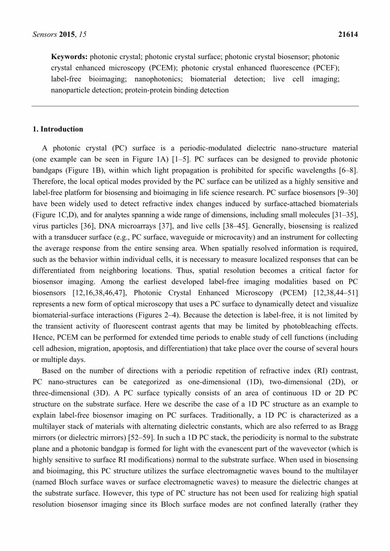
Figure 3. Instrument 2: Transmission acquisition mode of photonic crystal biosensor
integrated with an upright imaging microscope and using laser as light source.
(A) Schematic of combined label-free and enhanced-fluorescence imaging instrument;
(B) Enhanced (a) fluorescence and (b) label-free images of 50 mg/mL SA-Cy5 spots on a
PC biosensor. Inverted transmission versus angle response for a pixel inside and outside
the SA-Cy5 spot in (c), and cross-section of the label-free image through two SA-Cy5
spots in (d). Rather than measuring the PWS, the label-free imaging system measures the
angle of minimum transmission (AMT) by illuminating the PC sensor at a fixed
wavelength while scanning the angle of illumination through computer-controlled rotation
of the mirror (reprinted in part with permission from [76], © 2009 American Optical Society);
(C) Label-free image of a DNA microarray measured with a PC biosensor. The white
dashed box denotes the location of a set of 20 intentional blank spots. A line profile
running through a row containing 4 blank spots followed by 12 probe spots is shown
in (D) (Reprinted in part with permission from [37], © 2010 American Chemical Society).

Sensors 2015, 15 21618
Figure 4. Instrument 3: Reflection acquisition mode of photonic crystal biosensor
integrated with an inverted microscope and using LED as light source. (A) Schematic of
the structure of a photonic crystal (PC) surface biosensor with a surface-attached
nanoparticle, inset: photo of a PC biosensor fabricated on a glass slide; (B) Instrument
schematic of the modern Photonic Crystal Enhanced Microscopy (PCEM); (C) Scanning
electron micrograph of the photonic crystal surface, inset: zoomed-in image on the edge of
the PC biosensor; (D) Normalized spectrograph (surface plot) measured with PCEM. Inset:
PCEM-acquired 3D spectrum data; (E) AFM images of a tDPN-printed 3 × 3 array of
nano-dots (each with dimension of 5402 × 40 nm3), inset: zoomed-in AFM image of one
tDPN-printed dot; (F) PWV image of the tDPN-printed dots (displayed in a 3D surface
plot) within a 202 µm2 field of view, inset: 2D PWV image; (G) Normalized spectra of a
representative tDPN-printed dot and a background pixel, inset: zoomed-in image of the
spectra with 2D polynomial fitting (Reprinted in part with permission from [48], © 2014
RSC Publishing.).
The advantages of PCEM are inherent from the optical properties of slab-based PC surfaces, since
they can be designed as a wavelength-selective optical resonator and functionalized as a sensitive
optical transducer. For instance, high spatial resolution (in-plane) can be achieved in bioimaging due to
the restricted lateral propagation of electromagnetic waves on surface of the PC slab. Enhanced
electromagnetic fields (in the form of an evanescent field) near the PC surface (penetration depth of
~200 nm) only illuminate surface-adsorbed biomaterials, such as the extracellular matrix (ECM),
membrane components of surface-adsorbed cells, or cellular surface-attached nanoparticle tags. This
near-field high-intensity illumination regime promises a high axial resolution (out-of-plane) of
~200 nm, which is beyond the diffraction limit in the spectrum-range of the visible light (400–700 nm)
during bioimaging. Compared to the broadband resonances and lossy modes (due to absorption) on
metal surfaces, narrow line width (e.g., a few nm) resonant spectra and high reflection efficiency (e.g.,

Sensors 2015, 15 21619
nearly 100%) on dielectric surfaces of PC biosensors enable measurement of resonant wavelength
shifts with high spectral resolution. The PC resonant mode can be measured in a noncontact detection
instrument configuration, in which normal incident-angle illumination results in simple integration
with a standard microscope. The resonant wavelength can be selected on a PC surface by tuning its
geometry (e.g., grating period) or the incident angle of illumination. Thus, the sensing and imaging can
be realized in many spectral ranges, including ultraviolet, visible, and infrared (IR). Although PC
surfaces have been fabricated by expensive and time-consuming approaches (such as electron-beam
(e-beam) or nano-imprint lithography), recent developments in high-throughput and large-area
polymer-based techniques (such as nanoreplica molding at room temperature) have led to the
commercial introduction of single-use disposable PC sensors that can be manufactured in a roll-to-roll
fashion. These PC sensors can be subsequently integrated with standard format microplates,
microscope slides, and microfluidic devices for high-throughput drug or cytotoxicity screening of
biomolecule or cell assays. The goal of this review is to summarize the genesis, development, and
recent advances of PCEM.
2. Principles of Modern PCEM
2.1. Photonic Crystal Surface Biosensor
A dielectric PC surface (linear PC slab) is utilized as the optical transducer for RI sensing in the
label-free PCEM imaging system, as shown in Figure 4A. The PC surface is a resonant grating
structure with periodic modulation of the dielectric permittivity of a low-RI material in one dimension
(1D) (which provides the nano-pattern) and is then coated with a thin layer of high-RI material (which
supports the guided-mode resonances) [49,51]. When illuminated with broadband polarized light, the
incident light is coupled into the resonant modes of the PC if the Bragg condition is satisfied. As
mentioned earlier, such guided-mode resonances are referred to as “quasi guided modes” or “leaky
modes” since they are not allowed to propagate laterally (due to fact that these modes are rapidly
re-radiated out from the grating structure) and, thus, have a finite lifetime in the PC structure.
Therefore, the resulting electromagnetic standing waves that occur at the resonant wavelength inhibit
lateral propagation and open the potential for the PC surface to be utilized for label-free bioimaging.
At the combination of incident angle and incident wavelength that satisfies the resonant coupling
condition, nearly no light is transmitted through the PC and a high reflection coefficient (~100%) can
be achieved during bioimaging [1–3]. The input light can be coupled into the PC resonant mode via
wavelength or angle control, which does not require high precision position control and, thus, reduces
the complexity of the overall imaging instrument.
Fabrication of the PC surface can be performed upon large-area plastic sheets using a roll-to-roll
replica-molding procedure that is performed at room temperature [46,77–79]. The molding template,
which can be used repeatedly (up to thousands of times), can be made on silicon wafers or quartz
substrates by deep-UV lithography, nano-imprint lithography, or e-beam lithography. During the
replica-molding procedure, a thin layer of liquid ultraviolet-curable polymer (UVCP) (low-RI) is
deposited on the molding template and then compressed against the device substrate to create a
negative volume image of the grating structure from the mold. After exposure to high-intensity UV

Sensors 2015, 15 21620
light, the UVCP is cured to a solid-phase grating structure (e.g., grating period of Λ = 400 nm, grating
depth of d = 120 nm, duty cycle of f = 50%). A thin layer of high-RI material (e.g., titanium dioxide
(TiO2)) is subsequently deposited on top of the low-RI grating structure (UVCP), with its thickness
(e.g., thickness of t = 80 nm) selected to generate a resonant reflection at a specific wavelength (e.g.,
resonant wavelength of λ0 = 620 nm). A scanning electron microscope (SEM) image of a fabricated 1D
PC surface is shown in Figure 4C. This replica-molding method provides a rapid, reliable, and
inexpensive manufacturing process for PC surface fabrication.
The main criteria for measuring the performance of a PC surface biosensor include sensitivity and
spatial-resolution. The sensitivity of a PC biosensor is determined by the material (e.g., the dielectric
property of the high-RI layer) or the geometry of the nano-structure (e.g., the thickness of the high-RI
layer) [80]. The sensitivity can be estimated with Finite-difference time-domain (FDTD) computer
simulations and experimentally characterized with an optical transmission/reflection setup. As
mentioned earlier, the spatial resolution of the PC biosensor can be decomposed into in-plane and axial
resolution [81]. The in-plane resolution is characterized by the propagation length of resonant modes
along the surface plane of the nano-structure and the axial resolution is determined by the penetration
depth of the evanescent field atop of the PC surface. In addition, since the PC surface is an optical
biosensor, the selectivity is realized by coating the surface-immobilized antibody or ECM molecules
on the top of the biosensor. The absence of selectivity constraints on the biosensor avoids the specific
design for each application and, thus, enables a broad range of bio-applications for the PC biosensor.
2.2. PCEM Imaging Modality and Operating Principle
As shown in the schematic diagram (Figure 4B), the PCEM detection instrument uses a linear
scanning approach and is built upon the body of an inverted microscope (Carl Zeiss Axio Observer
Z1). In addition to ordinary brightfield imaging, a second illumination path is provided from a
fiber-coupled broadband LED, which is incident on the PC from below. The unpolarized LED output
light passes a polarized beam splitter (PBS) to illuminate the PC with light polarized with its axis
perpendicular to the grating lines (e.g., y direction), representing the transverse magnetic (TM) mode.
Since the resonant wavelength of a 1D PC surface is only sensitive to the incident angle in one angular
dimension (perpendicular to the grating) (y direction), the light can be focused in the orthogonal
angular dimension (parallel to the grating) (e.g., x direction) to strengthen the incident intensity.
Therefore, the light passing through the PBS is focused in one axis (x direction) by a cylindrical lens,
while the light remains collimated in the other angular dimension (y direction). The linear beam
(collimated direction) is focused on the back focal plane of the objective lens of the microscope. The
light emerging from the objective lens (upwards) is thus incident on the PC, so it is collimated in the
direction perpendicular to the PC grating lines (y direction) and, thus, all the light reaching the PC with
the TM polarization has the same angle of incidence. The reflected light beam passes through the
objective lens in the opposite direction (downwards), after which it is projected onto an imaging
spectrometer through a narrow entrance slit. The imaging spectrometer contains a diffraction grating
that disperses the wavelength components of the PC-reflected light. Once the spectrometer is
determined, the dimension of one imaged pixel of the PC in the direction parallel to the grating lines
(x direction) is determined by the magnification of the objective lens and the dimension of pixels

Sensors 2015, 15 21621
within the charge-coupled device (CCD) camera (Photometrics Cascade, 5122 pixels). A motorized
stage (Applied Scientific Instruments, MS2000) linearly translates the PC in the perpendicular
direction to the grating (y direction). The step-size of the stage (together with the magnifications of the
objective lens) determines the pixel size of the PCEM imaging system in the y direction. Therefore, a
large area can be scanned in a line-by-line fashion by translating the PC sensor in steps perpendicular
to the linear grating direction (y direction). For example, with a 10 × objective lens of the microscope,
a 16 µm2 pixel size of the CCD camera, and a 0.6 µm step size of the motorized stage, a final acquired
image with 0.62 µm2 pixel size can be measured in PCEM (with an acquisition speed of ~10 s per
frame for a scanning area of 3002 µm2).
For PCEM data acquisition, the linear light beam reflected from the PC that contains the resonant
biosensing signal produces a spatially resolved spectrum for each point along the line with a narrow
bandwidth (e.g., Δλ ~ 4 nm) and forms a 2D spectrograph (e.g., 5122 pixels) across the line (Figure 4D).
After line-by-line scanning, a 3D spectrum data (e.g., 5123 cube) can be acquired (Figure 4D inset) and
the signal/image processing can be performed with computational software (Matlab, MathWorks).
Specifically, the spectrum signal can be mathematically fit with a second-order polynomial or Lorentz
function for each pixel to extract the peak wavelength and intensity values. With a background
image acquired beforehand, shifts in the peak wavelength value (PWV) or shifts in the local peak
intensity value (PIV) can be calculated at each pixel location to measure the redistribution of the
attached biomaterials.
3. History of PCEM Development
The development of PCEM instrumentation can be described chronologically in three main phases
that have led to increasingly finer spatial-resolution and illumination/detection optics, which have been
designed for scanning biomolecular layers on dry PCs or cell attachment on PC surfaces exposed to
liquid media.
3.1. Instrument 1—Biomolecular Interaction Detection (BIND) Scanner
In 2002, the first PC biosensor introduced by SRU company (SRU Biosystems) was designed for
high-throughput microplate-based detection of protein-protein and protein-small molecule interactions,
using a PC with resonant reflection in the near-infrared (NIR) spectral range [49,51]. Shortly
afterwards, a PC biosensor microplate reader was introduced that incorporated a linear array of optical
fibers with illumination/detection heads that could read all the wells in one row (e.g., y direction) of a
96-well microplate at one time [46]. The illumination/detection heads were installed beneath the
microtiter plate, which sits upon a motion stage that could translate the plate in an orthogonal
dimension (e.g., x direction) to scan the entire microplate in ~15 s. This mode enabled serial
re-scanning of the microplate to generate kinetic data for the biomolecular interaction taking place in
all the wells. The PC biosensor resonant PWV was determined at each location with this linear scan
mode. Subsequently, the first-generation label-free PC biosensor imaging system was introduced and
named the “Biomolecular Interaction Detection” (BIND) Scanner (Instrument 1, Figure 2A) [12,47,50].
The optical fiber-based illumination/detection approach was replaced by free space illumination of the
bottom surface of the PC biosensor with a broadband light source, and the collection of reflected light

Sensors 2015, 15 21622
into an imaging spectrometer, which was able to rapidly acquire a spatial PWV map by scanning a
large sensor surface area. Following the light path of the system, the incoming light beam was divided
by a beam splitter, directed to the PC biosensor surface, magnified by an optional objective lens, and,
finally, projected into the imaging spectrometer via a narrow entrance slit. The illumination source in
this instrument was a white light lamp or a broadband light-emitting diode (LED) in the NIR spectral
range, and the detector was a CCD camera. In a single CCD image (Figure 2A, bottom-right inset), the
reflectance spectra of several hundred independent locations in one line that spans the PC were
gathered at one time. To construct a 2D PWV image, a scanning stage translated the PC across the
illumination line in small spatial increments.
The first generation of scanning PC imaging instruments (BIND Scanner) was developed
into a commercially available product and utilized in many life science research
applications [38–41,43,50,80,82,83]. For example, it has been reported in [83] that assessing combined
enhanced fluorescence and label-free biomolecular detection on the same PC surface. The sensitivity
of the PC biosensor has been examined in detail in [80]. The PWS image shown in Figure 2B
illustrates the detection of a microarray of Protein A printed on the biosensor surface to form the letters
‘NSG’ (Nano Sensors Group, University of Illinois at Urbana-Champaign) [50]. Cytotoxicity
screening of Bangladeshi medicinal plant extracts has been performed with pancreatic cancer cells
(Panc-1) using the BIND Scanner. As shown in Figure 2C, the untreated control group and two
representative plant extracts, Petunia punctata Paxton (P. punctate) and Anisoptera glabra Kurz (A. glabra),
demonstrate different cellular activities (apoptosis and proliferation) on the biosensor surfaces [41].
The imaging instrument was sufficient for observing large populations of cells with ~9 µm spatial
resolution, so that cells with large surface attachment footprints could be observed, although the
system lacked sufficient resolution for observing intra-cell attachment dynamics.
3.2. Instrument 2—Transmission Acquisition Mode with Upright Microscopy and Laser Source
To improve spatial resolution, an upright microscope (Olympus BX-51WI) was integrated into the
PC imaging system in 2009 [76] and the resulting system was named the “Photonic Crystal Enhanced
Microscope” [44]. Instead of measuring reflection efficiency as a function of wavelength from the
bottom of the PC surface, the second generation PCEM measured transmission efficiency as a
function of incident angle, using a fixed illumination wavelength from a beam-expanded laser
(Instrument 2, Figure 3A). This instrument was designed as a wide-field imaging system with
collimated angle-tunable laser illumination, which allowed imaging of a PC surface using the same
illumination source and imaging optics for both enhanced fluorescence (EF) and label-free (LF)
modalities. As shown in Figure 3A, the light beam generated from a HeNe laser passes through a
half-wave plate (for polarization control), a variable neutral density filter, a rotating diffuser (to reduce
speckle and fringes), a beam expander, an aperture, and a motorized angle-tunable mirror before
passing through the PC (which is positioned beneath the microscope objective lens). The
gimbal-mounted motorized mirror sits on top of a motorized linear stage in order to maintain a constant
illumination area on the PC device (as the mirror rotates) and provide selective light coupling to the
PC. Using this approach, high spatial-resolution and high sensitivity LF and EF images (Figure 3B)
can be accurately registered with each other since a common beam-path is shared for both imaging

Sensors 2015, 15 21623
modes [76]. An electron-multiplying (EM) CCD camera was used to acquire high resolution and
large-area images, and thus enable high-throughput analysis. Moreover, images can be simultaneously
acquired with other imaging techniques available on the EF/LF microscope, including reflected
brightfield (BF) and differential interference contrast (DIC) images that can be overlaid with EF and
LF images.
This transmission-based PC imaging modality that was capable of simultaneous label-free and
enhanced fluorescence imaging (EF/LF) was further developed and utilized in several follow-up
publications [20,41,42,44,76,81,84]. One of the main applications envisioned for the instrument was
for performing DNA and protein microarray analysis, in which the label-free image of immobilized
capture spots could be used to verify correct microarray printing and uniform spot density, while the
enhanced fluorescence imaging modality would be used after hybridization of the target molecules
from a test sample that carries fluorescent tags. Optimization of the imaging spatial resolution was
reported in [81]. Microplate, microfluidic channel, and spot-based affinity capture assays were also
demonstrated with this detection platform [84]. Figure 3C shows an example of a label-free image
acquired with a tunable resonant angle for a DNA microarray immobilized on the biosensor surface [37].
Figure 3D shows a line profile through a row (red line in Figure 3C) containing 4 blank spots followed
by 12 probe spots. It can be clearly observed that areas where the probe DNA has been immobilized
produce a measurable increase in the resonant angle.
3.3. Instrument 3—Reflection Acquisition Mode with Inverted Microscopy and LED Source
Recently, the PCEM instrumentation transitioned to its third generation, in which an inverted
microscope (Carl Zeiss Axio Observer Z1) body was chosen as the base of the system (Instrument 3,
Figure 4A,B) [45,48]. While the second generation PCEM was developed specifically for scanning PC
surfaces in a dry state for the detection of surface-adsorbed biomolecule patterns (such as DNA
microarrays), the third generation PCEM was designed for label-free detection of cells and real-time
detection of binding events in which the PC surface is exposed to liquid. In order to avoid scattering
and absorption or interference from cell bodies, microfluidic components, semi-opaque liquid media,
or liquid-air meniscus, bottom illumination of the PC was adopted in a reflection mode. In this system,
detection of resonant reflected wavelength shifts was adopted again as the sensing approach rather than
sensing changes in the resonant angle for a fixed illumination wavelength. An LED was chosen as the
light source to avoid the speckles in the acquired images that may be caused by a laser illumination
source. To obtain higher illumination intensity from the LED light source, a cylindrical lens was added
into the illumination light path to convert the incident light from a circular spot to a more concentrated
linear beam [45].
Label-free imaging of surface-absorbed live cells (including cell attachment, chemotaxis, and
apoptosis) [45] and nanoparticles [48] has been performed using the third generation PCEM.
Fluorescence-labeled imaging is also enabled in this system, in which the PC can be excited by a laser
illumination source that can couple with the resonant PC mode to obtain an electric field enhancement
effect. This enhancement is capable of increasing fluorescence detection sensitivity (which has been
validated previously [20,76,83,85–95]) and enabling estimation of the distance of fluorescence

Sensors 2015, 15 21624
emitters from the PC surface [96]. The most recently adopted PC surface design and PCEM detection
instrument configurations have already been described in detail in section 2.
4. Applications of PCEM
The PCEM imaging system can be applied to monitor kinetic changes in the spatial distribution of
dielectric permittivity for surface-adsorbed materials. This section describes PCEM applications with
several examples, such as label-free live cell imaging, nanoparticle and protein-protein binding
detection, and intensity enhancement of fluorescent tags embedded within live cells.
4.1. PCEM for Label-Free Live Cell Imaging
Label-free live cell imaging involves a sensing transducer surface, which typically generates an
electrical or optical signal when cells interact with it. Biosensors that measure intrinsic cellular
properties (such as dielectric permittivity) can be used to determine the number of cells in contact with
the transducer, or the distribution/redistribution of focal adhesion areas. Such transducers (e.g., PC
biosensors) may be prepared with different surface chemistry coatings that either mimic the in vivo
microenvironment within tissues or selectively capture specific cell populations through interaction
with proteins expressed on their outer cellular membranes. Therefore, the PCEM-based label-free
images of cell attachment can assist the study of cell-substrate interactions, including identifying,
capturing, and quantifying cells expressing specific surface molecules (Figure 2C) [38–45,50].
Recently, PCEM has been successfully demonstrated as a label-free live cell imaging approach to
provide visualizations of each individual cell with subcellular details [45]. As shown in Figure 5A–C,
Panc-1 cells were seeded onto a fibronectin-coated PC biosensor and allowed to incubate for 2 h
before imaging. The non-uniform distribution of the PWS and the subcellular activity can be visualized
clearly for each single cell. Figure 5B shows that the middle cell (No. 2) demonstrates higher PWS in
regions near the boundary of lamellipodia formation (consistent with the creation of actin bundles).
These darker shadings in the cell indicate regions of higher protein concentration, which may be
attributed to higher modulation in the strength of cellular material attachment.
In addition, the kinetics of dynamic interaction between cellular materials and surface coating
materials can be measured quantitatively using PCEM. As shown in Figure 5D, a sequence of movie
frames demonstrates murine dental stem cells (mHAT9a) gradually attaching on the PC surface. Cells
were seeded at 20,000 cells per mL on a fibronectin-coated PC biosensor surface. After three minutes,
initial cell attachment appears as small, round regions, which is consistent with spheroid, trypsinized
cells coming out of suspension and attaching to a surface. As time progresses, both the size of the cells
and intensity of the PWS induced by them increases, indicating a higher localization of cellular
material at the biosensor surface, which can be expected during cell spreading. Finally, once cells are
sufficiently attached, cellular processes can be observed sensing the cells’ microenvironment in all
directions. The outer irregular boundaries of the cells have a relatively low PWS (consistent with thin,
exploratory filopodia) accompanied by a more heavily attached region slightly immediately adjacent in
the cell interior (likely a result of actin bundle formation). Figure 5D illustrates distinct modulation
distributions of the attachment strength for both individual cells and the whole cell group during
different periods of the adhesion procedure.

Sensors 2015, 15 21625
Figure 5. Wavelength-sensitive live cell image from instrument 3–PCEM. (A) Brightfield
and (B) PWV images of Panc-1 cells attached to the PC surface. Lamellipodial extensions
are visible, especially from cell 2, demonstrating the ability of PCEM to resolve regional
differences in single-cell attachment; (C) Representative spectra (normalized) from
background regions and regions with cellular attachment. Selected areas of the PWV image
from beneath a cell show the PWS of a typical Panc-1 cell is ~1.0 nm; (D) Time-lapse
PWS images of cellular attachment of dental stem cells (mHAT9a) (Reprinted in part with
permission from [45], © 2013 RSC Publishing).
4.2. PCEM for Imaging of Nanoparticle and Protein-Protein Binding
Because the PC surface structure restricts lateral propagation of light at the resonant wavelength, it
is possible to create spatial maps of the resonant wavelength and the resonant damping that allow
high spatial resolution imaging of small-size biomaterials distributed across the surface. Particles
smaller than the pixel size (e.g., 6002 nm2 for our current PCEM) are very challenging to visualize and
identify. However, it is possible to detect the presence of individual particles when the PWS induced
by each particle is higher than the detection sensitivity limit of PCEM at each pixel location (the
noise-induced PWS need to be considered as well). It is noteworthy that the PWV image for a particle
is always within a diffraction-limited distance of up to five (or more) adjacent pixels and, hence, it is
not expected to observe a PWS of only one pixel when a sub-micron nanoparticle attaches to the PC.
As shown in Figure 4F, a PWV image is acquired for a 3 × 3 polystyrene particle array that is printed
by thermal Dip-Pen Nanolithography (tDPN) [97,98] with heated atomic force microscopy (AFM)
tips. Each particle has the dimension of ~5402 × 40 nm3 and ~5 µm gaps in between (Figure 4E).
Figure 4G demonstrates two acquired spectra (one from a pixel at particle location, and one from

Sensors 2015, 15 21626
background location) and each printed particle can cause ~0.5 nm PWS, which can be easily detected
and visualized using the PCEM system. Not only dielectric nanoparticles (as optical scatters) but also
metal nanoparticles (as optical absorbers) as small as ~100 nm can be detected via PIV-shift images
using PCEM [48].
Single nanoparticles allowing direct visualization in PCEM can be applied as biosensing tags to
detect protein-protein binding for multiple events on a large sensor surface synchronously. This
detection and imaging capability may be used in high-throughput screening during extended periods
while avoiding photobleaching issues that are inherent for fluorescence dye tags. Furthermore, the
resonance wavelength of nanoparticles can be conveniently tuned through the incident angle of the
illumination light [44], the dimension of the PC biosensor [80], and the size or geometry of the
nanoparticle [48,99,100]. An example is plotted in Figure 6 for PCEM detection of a target protein
molecule (e.g., Rabbit Immunoglobulin G (IgG)) binding with the immobilized capture antibodies
(e.g., anti-Rabbit IgG) using gold nanorods (AuNR) as tags [48]. The aspect ratio of the AuNR
(dimension of ~652 × 30 nm3) was tuned such that its localized surface plasmon resonance (LSPR)
matched the resonant wavelength of the PC biosensor, and thus further improved the signal-to-noise
ratio performance of the imaging system.
Figure 6. PCEM detection of protein-protein binding. (A) Schematic illustration of the
PCEM detection of protein-protein binding on the PC biosensor surface; (B) SEM images
of AuNR-IgG (AuNR conjugated with SH-PEG-IgG) attached to the PC biosensor surface.
Inset: zoomed-in image for one AuNR; (C) PCEM-detected peak intensity value (PIV)
images (in grayscale) and the PIV-shift image indicating AuNR-IgG attached on the PC
surface; (D) Two representative cross-section lines of the normalized intensity images
with/without two AuNRs-IgG on the PC surface (Reprinted in part with permission
from [48], © 2014 RSC Publishing.).
Sensors 2015, 15 21627
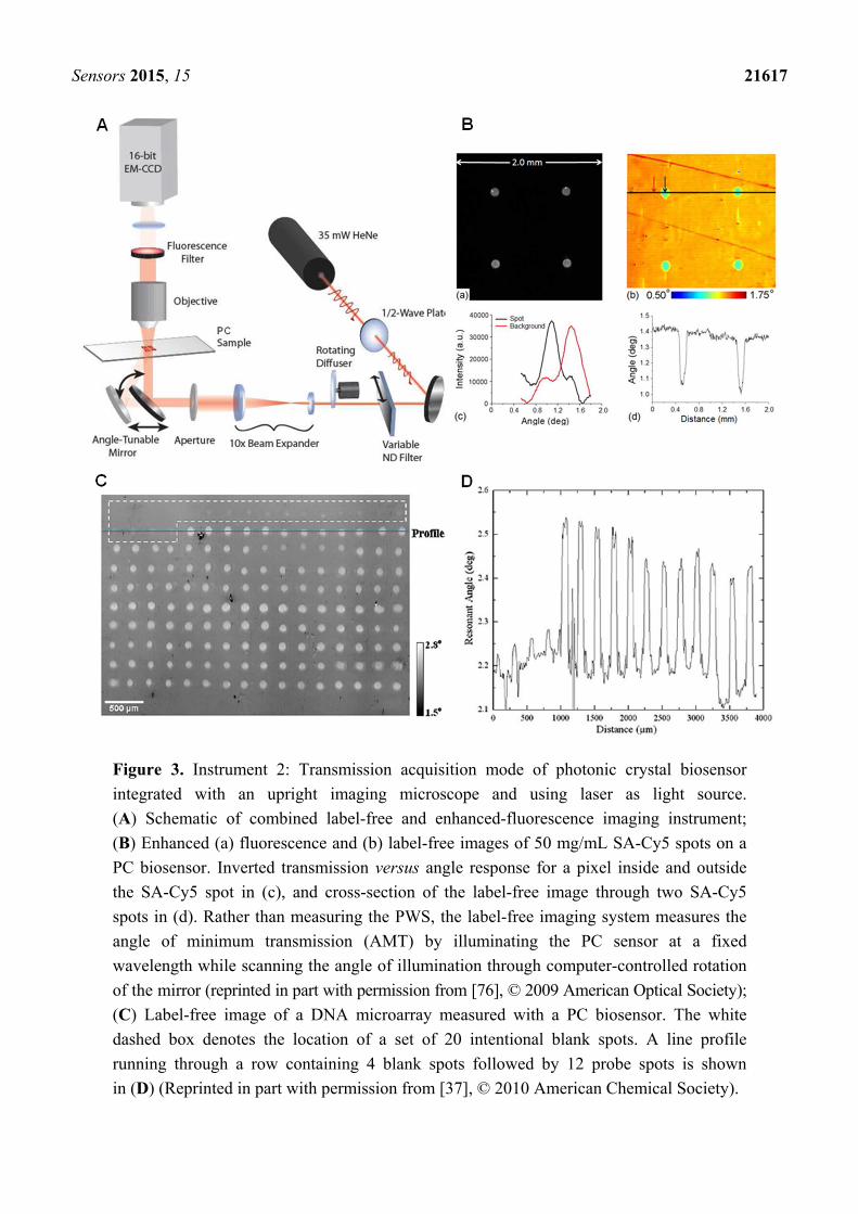
Figure 7. Photonic Crystal Enhanced Fluorescence (PCEF) portion on a PCEM imaging
system. (A) Schematic of the PCEF portion on modern PCEM detection instrumentation.
Inset (top left): angle reflection spectrum; (B) Brightfield and PCEF images of membrane
dye-stained 3T3 fibroblast cells: (a) brightfield, (b) off-resonance PCEF, (c) on-resonance
PCEF, (d) enhancement factor image, (e) 3D surface plot image of the enhancement factor
(Reprinted in part with permission from [96], © 2014 RSC Publishing).
4.3. Combination of PCEM and PCEF for Label-Free/Fluorescence-Labeled Imaging Simultaneously
The PCEM is not limited to detection of optical scatters or absorbers, but is also capable of
enhancing the emission and extraction from optical emitters (such as fluorescent dyes) in the
evanescent field of the PC biosensor. Based on this principle, the label-free PCEM system can be
slightly modified to include an additional illumination path from a laser that can excite fluorescent
emitters. The ability to tune the illumination angle of the laser to match the resonant coupling

Sensors 2015, 15 21628
condition of the PC substantially enhances the electric field intensity that is used to excite
fluorophores, resulting in higher intensity fluorescence microscope images. Photonic Crystal Enhanced
Fluorescence (PCEF) represents an additional imaging modality within the PCEM that enables rapid
switching between label-free and fluorescence-labeled imaging modes (Figure 3A) [76,83]. Figure 3B
demonstrates the enhanced fluorescence image and the label-free image of the same microarray spots
printed with cyanine-5-tagged streptavidin (Cy5-SA) proteins. Figure 7A depicts the current optical
setup for the PCEF portion of a combined imaging system. Illumination from a fiber-coupled
semiconductor laser diode is collimated and passed through a half waveplate to produce a polarization
perpendicular to the PC grating lines. Figure 7A inset (top left) plots an angle reflection spectrum of
the PC surface when illuminated with a collimated semiconductor laser at 637 nm over a range of
illumination angles. Maximum reflection intensity occurs at the on-resonance condition at an incident
angle of ±1.14° from normal direction. The off-resonance condition refers to the laser illumination
at an incidence angle of 5°. Figure 7B illustrates the corresponding enhanced fluorescence images
for membrane dye-stained 3T3 fibroblast cells [96]. The combination of both modalities
extends the PC-enhanced imaging system to be multi-functional and capable of imaging in
numerous bio-applications.
5. Summary
Nanophotonic surfaces used in label-free biosensing and bioimaging are an attractive research area
and have been involved in many biological applications, including disease diagnostics, drug discovery,
and the fundamental study of molecular and cellular activity/function. Detection and imaging tools
utilizing nanophotonic surfaces (such as PCEM) with high sensitivity, high detection throughput, and
inexpensively manufactured sensors are demanding requirements for life science research and drug
discovery applications. This paper reviewed the principles and applications along with the
development history of PCEM, which utilizes a photonic crystal surface as an optical transducer to
detect and visualize surface-absorbed biomaterials. PCEM achieves high sensitivity and high
spatial-resolution due to the narrow spectra line width, restricted lateral propagation and evanescent
field enhancement on the PC surface. The PC-enhanced imaging system can be applied to the
quantitative and dynamic measurement of cell-substrate interactions, nanoparticle attachment, and
protein-protein binding on the biosensor surface. PCEM can also be combined with PCEF to construct
a versatile imaging system for tracking and visualizing different optical phenomena that occur within
an individual sample. This novel imaging system opens new routes for the detection and visualization
of surface-attached biomaterials and holds great potential to help uncover numerous underlying
biological mechanisms.
Acknowledgments
This work is supported by the National Science Foundation (NSF Grant CBET 0427657, CBET
0754122, CBET 1132301) and National Institutes of Health (NIH R01 CA118562, R01 GM086382).
The authors would like to thank the Nano Sensors Group (NSG) and staff in Micro and
Nanotechnology Laboratory (MNTL), the Center for innovative instrumentation Technology (CiiT) at
University of Illinois at Urbana-Champaign for their support.

Sensors 2015, 15 21629
Conflicts of Interest
The authors declare no conflict of interest.
References
1. Hessel, A.; Oliner, A.A. A new theory of wood’s anomalies on optical gratings. Appl. Opt. 1965,
4, 1275–1297.
2. Mashev, L.; Popov, E. Diffraction efficiency anomalies of multicoated dielectric gratings.
Opt. Commun. 1984, 51, 131–136.
3. Popov, E.; Mashev, L.; Maystre, D. Theoretical study of the anomalies of coated dielectric
gratings. Opt. Acta 1986, 33, 607–619.
4. Yablonovitch, E. Inhibited spontaneous emission in solid-state physics and electronics.
Phys. Rev. Lett. 1987, 58, 2059–2062.
5. John, S. Strong localization of photons in certain disordered dielectric superlattices. Phys. Rev.
Lett. 1987, 58, 2486–2489.
6. Joannopoulos, J.D.; Villeneuve, P.R.; Fan, S. Photonic crystals: Putting a new twist on light.
Nature 1997, 386, 143–149.
7. Fan, S.H.; Joannopoulos, J.D. Analysis of guided resonances in photonic crystal slabs. Phys. Rev. B
2002, 65, 235112.
8. Joannopoulos, J.D.; Johnson, S.G.; Winn, J.N.; Meade, R.D. Photonic Crystals: Molding the
Flow of Light, 2nd ed.; Princeton University Press: Princeton, NJ, USA, 2008.
9. Magnusson, R.; Wang, S.S. New principle for optical filters. Appl. Phys. Lett. 1992, 61, 1022–1024.
10. Kikuta, H.; Maegawa, N.; Mizutani, A.; Iwata, K.; Toyota, H. Refractive index sensor with a
guided-mode resonant grating filter. Proc. SPIE 2001, 4416, 219–222.
11. Villa, F.; Regalado, L.E.; Ramos-Mendieta, F.; Gaspar-Armenta, J.; Lopez-Rios, T. Photonic
crystal sensor based on surface waves for thin-film characterization. Opt. Lett. 2002, 27, 646–648.
12. Cunningham, B.T.; Li, P.; Schulz, S.; Lin, B.; Baird, C.; Gerstenmaier, J.; Genick, C.; Wang, F.;
Fine, E.; Laing, L. Label-free assays on the bind system. J. Biomol. Screen. 2004, 9, 481–490.
13. Fang, Y.; Ferrie, A.M.; Fontaine, N.H.; Mauro, J.; Balakrishnan, J. Resonant waveguide grating
biosensor for living cell sensing. Biophys. J. 2006, 91, 1925–1940.
14. Skivesen, N.; Tetu, A.; Kristensen, M.; Kjems, J.; Frandsen, L.H.; Borel, P.I. Photonic-crystal
waveguide biosensor. Opt. Expr. 2007, 15, 3169–3176.
15. Konopsky, V.N.; Alieva, E.V. Photonic crystal surface waves for optical biosensors. Anal. Chem.
2007, 79, 4729–4735.
16. Nazirizadeh, Y.; Geyer, U.; Lemmer, U.; Gerken, M. Spatially resolved optical characterization
of photonic crystal slabs using direct evaluation of photonic modes. In Proceedings of the IEEE
International Conference on Optical MEMs and Nanophotonics, Freiburg, Gremany, 11 August
2008; pp. 112–113.
17. Guo, Y.B.; Divin, C.; Myc, A.; Terry, F.L.; Baker, J.R.; Norris, T.B.; Ye, J.Y. Sensitive
molecular binding assay using a photonic crystal structure in total internal reflection. Opt. Expr.
2008, 16, 11741–11749.

Sensors 2015, 15 21630
18. Fang, Y.; Frutos, A.G.; Verklereen, R. Label-free cell-based assays for gpcr screening.
Comb. Chem. High Throughput Screen. 2008, 11, 357–369.
19. Konopsky, V.N.; Alieva, E.V. Optical biosensors based on photonic crystal surface waves.
Methods Mol. Biol. 2009, 503, 49–64.
20. Cunningham, B.T. Photonic crystal surfaces as a general purpose platform for label-free and
fluorescent assays. JALA Charlottesv Va 2010, 15, 120–135.
21. El Beheiry, M.; Liu, V.; Fan, S.; Levi, O. Sensitivity enhancement in photonic crystal slab
biosensors. Opt. Expr. 2010, 18, 22702–22714.
22. Nazirizadeh, Y.; Bog, U.; Sekula, S.; Mappes, T.; Lemmer, U.; Gerken, M. Low-cost label-free
biosensors using photonic crystals embedded between crossed polarizers. Opt. Expr. 2010, 18,
19120–19128.
23. Jamois, C.; Li, C.; Gerelli, E.; Orobtchouk, R.; Benyattou, T.; Belarouci, A.; Chevolot, Y.;
Monnier, V.; Souteyrand, E. New Concepts of Integrated Photonic Biosensors Based on Porous
Silicon. In Biosensors-Emerging Materials and Applications; Serra, P.A., Ed.; InTech: Rijeka,
Croatia, 2011.
24. Magnusson, R.; Wawro, D.; Zimmerman, S.; Ding, Y. Resonant photonic biosensors with
polarization-based multiparametric discrimination in each channel. Sensors 2011, 11, 1476–1488.
25. Nazirizadeh, Y.; Becker, T.; Reverey, J.; Selhuber-Unkel, C.; Rapoport, D.H.; Lemmer, U.;
Gerken, M. Photonic crystal slabs for surface contrast enhancement in microscopy of transparent
objects. Opt. Expr. 2012, 20, 14451–14459.
26. Pal, S.; Fauchet , P.M.; Miller, B.L. 1-d and 2-d photonic crystals as optical methods for
amplifying biomolecular recognition. Anal.Chem. 2012, 84, 8900–8908.
27. Threm, D.; Nazirizadeh, Y.; Gerken, M. Photonic crystal biosensors towards on-chip integration.
J. Biophotonics 2012, 5, 601–616.
28. Carbonell, J.; Diaz-Rubio, A.; Torrent, D.; Cervera, F.; Kirleis, M.A.; Pique, A.; Sanchez-Dehesa, J.
Radial photonic crystal for detection of frequency and position of radiation sources. Sci. Rep.
2012, 2, 558.
29. Grepstad, J.O.; Kaspar, P.; Solgaard, O.; Johansen, I.R.; Sudbo, A.S. Photonic-crystal
membranes for optical detection of single nano-particles, designed for biosensor application.
Opt. Expr. 2012, 20, 7954–7956.
30. Troia, B.; Paolicelli, A.; Leonardis, F.D.; Passaro, V.M.N. Photonic crystals for optical sensing:
A review. In Advances in Photonic Crystals; Passaro, V.M.N., Ed.; InTech: Rijeka, Croatia, 2013.
31. Lin, B.; Qiu, J.; Gerstenmeier, J.; Li, P.; Pien, H.; Pepper, J.; Cunningham, B. A label-free optical
technique for detecting small molecule interactions. Biosens. Bioelectron. 2002, 17, 827–834.
32. Chan, L.L.; Cunningham, B.T.; Li, P.Y.; Puff, D. A self-referencing method for microplate
label-free photonic-crystal biosensors. IEEE Sens. J. 2006, 6, 1551–1556.
33. Chan, L.L.; Lidstone, E.A.; Finch, K.E.; Heeres, J.T.; Hergenrother, P.J.; Cunningham, B.T. A
method for identifying small molecule aggregators using photonic crystal biosensor microplates.
J. Assoc. Lab. Autom. 2009, 14, 348–359.
34. Ge, C.; Lu, M.; George, S.; Flood, T.A.; Wagner, C.; Zheng, J.; Pokhriyal, A.; Eden, J.G.;
Hergenrother, P.J.; Cunningham, B.T. External cavity laser biosensor. Lab Chip 2013, 13,
1247–1256.

Sensors 2015, 15 21631
35. Zhang, M.; Peh, J.; Hergenrother, P.J.; Cunningham, B.T. Detection of protein-small molecule
binding using a self-referencing external cavity laser biosensor. J. Am. Chem. Soc. 2014, 136,
5840–5843.
36. Shafiee, H.; Lidstone, E.A.; Jahangir, M.; Inci, F.; Hanhauser, E.; Henrich, T.J.; Kuritzkes, D.R.;
Cunningham, B.T.; Demirci, U. Nanostructured optical photonic crystal biosensor for HIV viral
load measurement. Sci. Rep. 2014, 4, 4116.
37. George, S.; Block, I.D.; Jones, S.I.; Mathias, P.C.; Chaudhery, V.; Vuttipittayamongkol, P.;
Wu, H.Y.; Vodkin, L.O.; Cunningham, B.T. Label-free prehybridization DNA microarray
imaging using photonic crystals for quantitative spot quality analysis. Anal. Chem. 2010, 82,
8551–8557.
38. Lin, B.; Li, P.; Cunningham, B.T. A label-free biosensor-based cell attachment assay for
characterization of cell surface molecules. Sens. Actuators B Chem. 2006, 114, 559–564.
39. Chan, L.L.; Gosangari, S.L.; Watkin, K.L.; Cunningham, B.T. A label-free photonic crystal
biosensor imaging method for detection of cancer cell cytotoxicity and proliferation. Apoptosis
2007, 12, 1061–1068.
40. Chan, L.L.; Gosangari, S.L.; Watkin, K.L.; Cunningham, B.T. Label-free imaging of cancer cells
using photonic crystal biosensors and application to cytotoxicity screening of a natural compound
library. Sens. Actuators B Chem. 2008, 132, 418–425.
41. George, S.; Bhalerao, S.V.; Lidstone, E.A.; Ahmad, I.S.; Abbasi, A.; Cunningham, B.T.;
Watkin, K.L. Cytotoxicity screening of bangladeshi medicinal plant extracts on pancreatic cancer
cells. Complement. Altern. Med. 2010, 10, 52.
42. Shamah, S.M.; Cunningham, B.T. Label-free cell-based assays using photonic crystal optical
biosensors. Analyst 2011, 136, 1090–1102.
43. Chan, L.L.; George, S.; Ahmad, I.; Gosangari, S.L.; Abbasi, A.; Cunningham, B.T.; Watkin, K.L.
Cytotoxicity effects of amoorarohituka and chittagonga on breast and pancreatic cancer cells.
Complement. Altern. Med. 2011, 10, 1–8.
44. Lidstone, E.A.; Chaudhery, V.; Kohl, A.; Chan, V.; Wolf-Jensen, T.; Schook, L.B.; Bashir, R.;
Cunningham, B.T. Label-free imaging of cell attachment with photonic crystal enhanced
microscopy. Analyst 2011, 136, 3608–3615.
45. Chen, W.L.; Long, K.D.; Lu, M.; Chaudhery, V.; Yu, H.; Choi, J.S.; Polans, J.; Zhuo, Y.;
Harley, B.A.C.; Cunningham, B.T. Photonic crystal enhanced microscopy for imaging of live cell
adhesion. Analyst 2013, 138, 5886–5894.
46. Cunningham, B.T.; Qiu, J.; Li, P.; Pepper, J.; Hugh, B. A plastic colorimetric resonant optical
biosensor for multiparallel detection of label-free biochemical interactions. Sens. Actuators B
Chem. 2002, 85, 219–226.
47. Li, P.; Lin, B.; Gerstenmaier, J.; Cunningham, B.T. A new method for label-free imaging of
biomolecular interactions. Sens. Actuators B Chem. 2004, 99, 6–13.
48. Zhuo, Y.; Hu, H.; Chen, W.L.; Lu, M.; Tian, L.M.; Yu, H.J.; Long, K.D.; Chow, E.; King, W.P.;
Singamaneni, S.; et al. Single nanoparticle detection using photonic crystal enhanced microscopy.
Analyst 2014, 139, 1007–1015.
49. Cunningham, B.; Qiu, J.; Li, P.; Lin, B. Enhancing the surface sensitivity of colorimetric
resonant optical biosensors. Sens. Actuators B Chem. 2002, 87, 365–370.

Sensors 2015, 15 21632
50. Cunningham, B.T.; Laing, L. Microplate-based, label-free detection of biomolecular interactions:
Applications in proteomics. Expert Rev. Proteom. 2006, 3, 271–281.
51. Cunningham, B.T.; Li, P.; Lin, B.; Pepper, J. Colorimetric resonant reflection as a direct
biochemical assay technique. Sens. Actuators B Chem. 2002, 81, 316–328.
52. Yeh, P.; Yariv, A.; Cho, A.Y. Optical surface waves in periodic layered media. Appl. Phys. Lett.
1978, 32, 104–105.
53. Meade, R.D.; Brommer, K.D.; Rappe, A.M.; Joannopoulos, J.D. Electromagnetic bloch waves at
the surface of a photonic crystal. Phys. Rev. B 1991, 44, 10961–10964.
54. Robertson, W.M.; May, M.S. Surface electromagnetic wave excitation on one-dimensional
photonic band gap arrays. Appl. Phys. Lett. 1999, 74, 1800–1802.
55. Shinn, M.; Robertson, W.M. Surface plasmon-like sensor based on surface electromagnetic
waves in a photonic band gap material. Sens. Actuators B Chem. 2005, 105, 360–364.
56. Descrovi, E.; Frascella, F.; Sciacca, B.; Geobaldo, F.; Dominici, L.; Michelotti, F. Coupling of
surface waves in highly defined one-dimensional porous silicon photonic crystals for gas sensing
applications. Appl. Phys. Lett. 2007, 91, 241109-1–241109-3.
57. Sfez, T.; Descrovi, E.; Dominici, L.; Nakagawa, W.; Michelotti, F.; Giorgis, F.; Herzig, H.P.
Near-field analysis of surface electromagnetic waves in the bandgap region of a polymeric
grating written on a one-dimensional photonic crystal. Appl. Phys. Lett. 2008, 93,
061108-1–061108-3.
58. Sinibaldi, A.; Danz, N.; Descrovi, E.; Munzertb, P.; Schulz, U.; Sonntag, F.; Dominici, L.;
Michelotti, F. Direct comparison of the performance of bloch surface wave and surface plasmon
polariton sensors. Sens. Actuators B Chem. 2012, 174, 292–298.
59. Li, Y.; Yang, T.; Pang, Z.; Du, G.; Song, S.; Han, S. Phase-sensitive bloch surface wave sensor
based on variable angle spectroscopic ellipsometry. Opt. Expr. 2014, 22, 21403–21410.
60. Fan, S.; Villeneuve, P.R.; Joannopoulos, J.D.; Schubert, E.F. High extraction efficiency of
spontaneous emission from slabs of photonic crystals. Phys. Rev. Lett. 1997, 18, 3294–3297.
61. Kanskar, M.; Paddon, P.; Pacradouni, V.; Morin, R.; Busch, A.; Young, J.F.; Johnson, S.R.;
MacKenzie, J.; Tiedje, T. Observation of leaky slab modes in an air-bridged semiconductor
waveguide with a two-dimensional photonic lattice Appl. Phys. Lett. 1997, 70, 1438–1440.
62. Villeneuve, P.R.; Fan, S.; Johnson, S.G.; Joannopoulos, J.D. Three-dimensional photon
confinement in photonic crystals of low-dimensional periodicity. IEEE Proc. Optoelectron. 1998,
145, 384–390.
63. Johnson, S.G.; Fan, S.; Villeneuve, P.R.; Joannopoulos, J.D.; Kolodziejski, L.A. Guided modes
in photonic crystal slabs. Phys. Rev. B 1999, 60, 5751–5758.
64. Painter, O.; Vuckovic, J.; Scherer, A. Defect modes of a two-dimensional photonic crystal in an
optically thin dielectric slab. J. Opt. Soc. Am. B 1999, 16, 275–285.
65. Boroditsky, M.; Vrijen, R.; Krauss, T.F.; Coccioli, R.; Bhat, R.; Yablonovitch, E. Spontaneous
emission extraction and purcell enhancement from thin-film 2-d photonic crystals.
Lightwave Technol. 1999, 17, 2096–2112.
66. Astratov, V.N.; Culshaw, I.S.; Stevenson, R.M.; Whittaker, D.M.; Skolnick, M.S.; Krauss, T.F.;
de la Rue, R.M. Resonant coupling of near-infrared radiation to photonic band structure
waveguides. Lightwave Technol. 1999, 17, 2050–2057.

Sensors 2015, 15 21633
67. Baba, T.; Fukaya, N.; Yonekura, J. Observation of light propagation in photonic crystal optical
waveguides with bends. Electron. Lett. 1999, 35, 654–655.
68. Paddon, P.; Young, J.F. Two-dimensional vector-coupled-mode theory for textured planar
waveguides. Phys. Rev. B 2000, 61, 2090–2101.
69. Pacradouni, V.; Mandeville, W.J.; Cowan, A.R.; Paddon, P.; Young, J.F.; Johnson, S.R. Photonic
band structure of dielectric membranes periodically textured in two dimensions. Phys. Rev. B
2000, 62, 4204–4207.
70. Kuchinsky, S.; Allan, D.C.; Borrelli, N.F.; Cotteverte, J.C. 3D localization in a channel
waveguide in a photonic crystal with 2d periodicity. Opt. Commun. 2000, 175, 147–152.
71. Lin, S.Y.; Chow, E.; Johnson, S.G.; Joannopoulos, J.D. Demonstration of highly efficient
waveguiding in a photonic crystal slab at the 1.5-um wavelength. Opt. Lett. 2000, 25,
1297–1299.
72. Benisty, H.; Labilloy, D.; Weisbuch, C.; Smith, C.J.M.; Krauss, T.F.; Cassagne, D.; Beraud, A.;
Jouanin, C. Radiation losses of waveguide-based two-dimensional photonic crystals: Positive
role of the substrate. Appl. Phys. Lett. 2000, 76, 532–534.
73. Chutinan, A.; Noda, S. Waveguides and waveguide bends in two-dimensional photonic crystal
slabs. Phys. Rev. B 2000, 62, 4488–4492.
74. Cowan, A.R.; Paddon, P.; Pacradouni, V.; Young, J.F. Resonant scattering and mode coupling in
two-dimensional textured planar waveguides. J. Opt. Soc. Am. A 2001, 18, 1160–1170.
75. Vahala, K. Optical Microcavities (Advanced Series in Applied Physics), 1st ed.; World Scientifc
Pubishing Company: Singapore, 2004.
76. Block, I.D.; Mathias, P.C.; Ganesh, N.; Jones, I.D.; Dorvel, B.R.; Chaudhery, V.; Vodkin, L.;
Bashir, R.; Cunningham, B.T. A detection instrument for enhanced fluorescence and label-free
imaging on photonic crystal surfaces. Opt. Expr. 2009, 17, 13222–13235.
77. Schulz, S.C. Web based photonic crystal biosensors for drug discovery & diagnostics. Vac. Coat.
2008, 68.
78. Krebs, F.C. Polymer solar cell modules prepared using roll-to-roll methods: Knife-over-edge
coating, slot-die coating and screen printing. Sol. Energy Mater. Sol. Cells 2009, 93, 465–475.
79. Ge, C.; Lu, M.; Jian, X.; Tan, Y.F.; Cunningham, B.T. Large-area organic distributed feedback
laser fabricated by nanoreplica molding and horizontal dipping. Opt. Expr. 2010, 18,
12980–12991.
80. Block, I.D.; Ganesh, N.; Lu, M.; Cunningham, B.T. A sensitivity model for predicting photonic
crystal biosensor performance. IEEE Sens. J. 2008, 8, 274–280.
81. Block, I.D.; Mathias, P.C.; Jones, S.I.; Vodkin, L.O.; Cunningham, B.T. Optimizing the spatial
resolution of photonic crystal label-free imaging. Appl. Opt. 2009, 48, 6567–6574.
82. Choi, C.J.; Cunningham, B.T. Single-step fabrication and characterization of photonic crystal
biosensors with polymer microfluidic channels. Lab Chip 2006, 6, 1373–1380.
83. Mathias, P.C.; Ganesh, N.; Chan, L.L.; Cunningham, B.T. Combined enhanced fluorescence and
label-free biomolecular detection with a photonic crystal surface. Appl. Opt. 2007, 46,
2351–2360.

Sensors 2015, 15 21634
84. Choi, C.J.; Belobraydich, A.R.; Chan, L.L.; Mathias, P.C.; Cunningham, B.T. Comparison of
label-free biosensing in microplate, microfluidic, and spot-based affinity capture assays.
Anal. Biochem. 2010, 405, 1–10.
85. Ganesh, N.; Zhang, W.; Mathias, P.C.; Chow, E.; Soares, J.A.; Malyarchuk, V.; Smith, A.D.;
Cunningham, B.T. Enhanced fluorescence emission from quantum dots on a photonic crystal
surface. Nat. Nanotechnol. 2007, 2, 515–520.
86. Ganesh, N.; Block, I.D.; Mathias, P.C.; Zhang, W.; Chow, E.; Malyarchuk, V.; Cunningham, B.T.
Leaky-mode assisted fluorescence extraction: Application to fluorescence enhancement
biosensors. Opt. Expr. 2008, 16, 21626–21640.
87. Ganesh, N.; Mathias, P.C.; Zhang, W.; Cunningham, B.T. Distance dependence of fluorescence
enhancement from photonic crystal surfaces. J. Appl. Phys. 2008, 103, 083104.
88. Pokhriyal, A.; Lu, M.; Huang, C.S.; Schulz, S.; Cunningham, B.T. Multicolor fluorescence
enhancement from a photonics crystal surface. Appl. Phys. Lett. 2010, 97, 121108.
89. Pokhriyal, A.; Lu, M.; Chaudhery, V.; Huang, C.S.; Schulz, S.; Cunningham, B.T. Photonic
crystal enhanced fluorescence using a quartz substrate to reduce limits of detection. Opt. Expr.
2010, 18, 24793–24808.
90. Mathias, P.C.; Ganesh, N.; Zhang, W.; Cunningham, B.T. Graded wavelength one-dimensional
photonic crystal reveals spectral characteristics of enhanced fluorescence. J. Appl. Phys 2008,
103, 094320.
91. Mathias, P.C.; Wu, H.Y.; Cunningham, B.T. Employing two distinct photonic crystal resonances
to improve fluorescence enhancement. Appl. Phys. Lett. 2009, 95, 201111.
92. Wu, H.Y.; Zhang, W.; Mathias, P.C.; Cunningham, B.T. Magnification of photonic crystal
fluorescence enhancement via tm resonance excitation and te resonance extraction on a dielectric
nanorod surface. Nanotechnology 2010, 21, 125203.
93. Chaudhery, V.; Lu, M.; Pokhriyal, A.; Schulz, S.C.; Cunningham, B.T. Angle-scanning photonic
crystal enhanced fluorescence microscopy. IEEE Sens. J. 2012, 12, 1272–1279.
94. George, S.; Chaudhery, V.; Lu, M.; Takagi, M.; Amro, N.; Pokhriyal, A.; Tan, Y.F.; Ferreira, P.;
Cunningham, B.T. Sensitive detection of protein and mirna cancer biomarkers using
silicon-based photonic crystals and a resonance coupling laser scanning platform. Lab Chip 2013,
13, 4053–4064.
95. Pokhriyal, A.; Lu, M.; Ge, C.; Cunningham, B.T. Coupled external cavity photonic crystal
enhanced fluorescence. J. Biophotonics 2014, 7, 332–340.
96. Chen, W.L.; Long, K.D.; Yu, H.J.; Tan, Y.F.; Choi, J.S.; Harley, B.A.; Cunningham, B.T.
Enhanced live cell imaging via photonic crystal enhanced fluorescence microscopy. Analyst
2014, 139, 5954–5963.
97. Hu, H.; Mohseni, P.K.; Pan, L.; Li, X.; Somnath, S.; Felts, J.R.; Shannon, M.A.; King, W.P.
Fabrication of arbitrarily-shaped silicon and silicon oxide nanostructures using tip-based
nanofabrication. J. Vac. Sci. Technol. B 2013, 31, 06FJ01.
98. King, W.P.; Bhatia, B.; Felts, J.R.; Kim, H.J.; Kwon, B.; Lee, B.; Somnath, S.; Rosenberger, M.
Heated atomic force microscope cantilevers and their applications. Annu. Rev. Heat Transf. 2013,
16, 287–326.
Sensors 2015, 15 21635
99. Tian, L.; Chen, E.; Gandra, N.; Abbas, A.; Singamaneni, S. Gold nanorods as plasmonic
nanotransducers: Distance-dependent refractive index sensitivity. Langmuir 2012, 28, 17435–17442.
100. Tian, L.; Morrissey, J.J.; Kattumenu, R.; Gandra, N.; Kharasch, E.D.; Singamaneni, S.
Bioplasmonic paper as a platform for detection of kidney cancer biomarkers. Anal. Chem. 2012,
84, 9928–9934.
© 2015 by the authors; licensee MDPI, Basel, Switzerland. This article is an open access article
distributed under the terms and conditions of the Creative Commons Attribution license
(http://creativecommons.org/licenses/by/4.0/).