lab manual for digital logic design - pddc...
TRANSCRIPT

L.D. COLLEGE OF ENGINEERING,AHMEDABAD
Lab Manual For
Digital Logic Design B.E. Semester III
Electronics & Communication Department
7/16/2012
NAME…………………………………………………. CLASS …………………….. ENROLLMENT NO.…………………………………… BATCH……………… LAB PARTNERS………………………………………….
Sima Gosai

USEFUL ICs
IC NUMBER Description of IC
7400 Quad 2 input NAND GATE 7401 Quad 2input NAND Gate (open collector) 7402 Quad 2 input NOR Gate 7403 Quad 2 input NOR Gates (open collector) 7404 Hex Inverts 7408 Quad 2 input AND Gate 7421 Dual 4 input AND Gate 7430 8 input NAND Gate 7432 Quad 2 input OR Gate 7486 Quad 2 input EX-OR Gate 74107 Dual J-K Flip Flop 74109 Dual J-K Flip Flop with Set and Reset 74173 Quad D Flip Flop 74174 Hex D Flip Flop 7473 Dual Master-Slave J-K Flip Flop 7474 Dual D Flip Flop 7475 Quad Bi-stable latch 7476 Dual J-K Flip Flop with Preset and Clear

7400(Quad 2 Input NAND)
Useful IC Pin detail
7402(Quad 2 Input NOR)
7404 Hex Inverter (NOT)
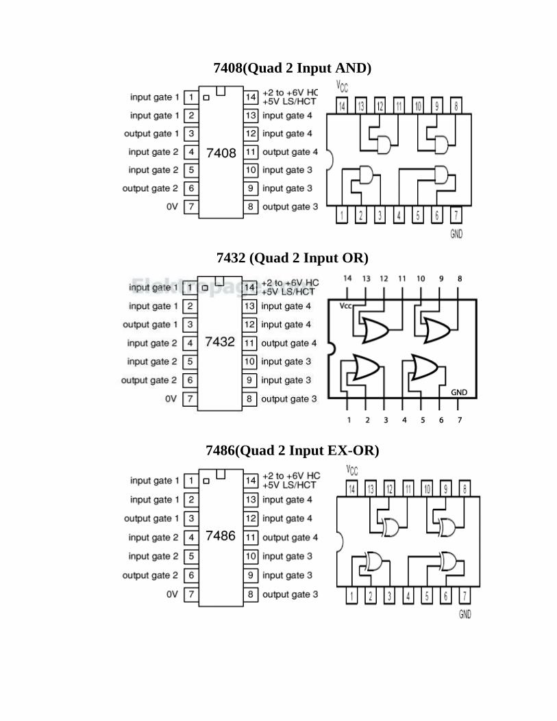
7408(Quad 2 Input AND)
7432 (Quad 2 Input OR)
7486(Quad 2 Input EX-OR)
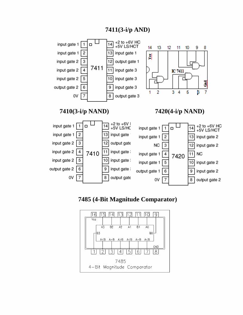
7411(3-i/p AND)
7410(3-i/p NAND) 7420(4-i/p NAND)
7485 (4-Bit Magnitude Comparator)
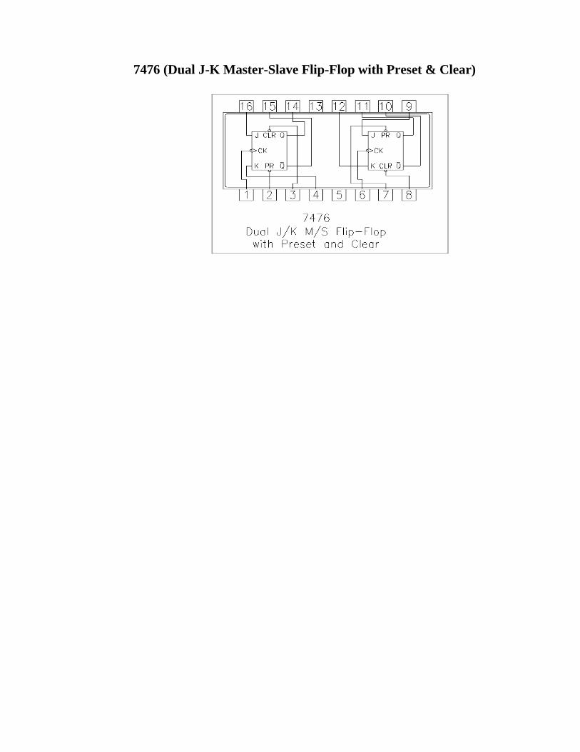
7476 (Dual J-K Master-Slave Flip-Flop with Preset & Clear)
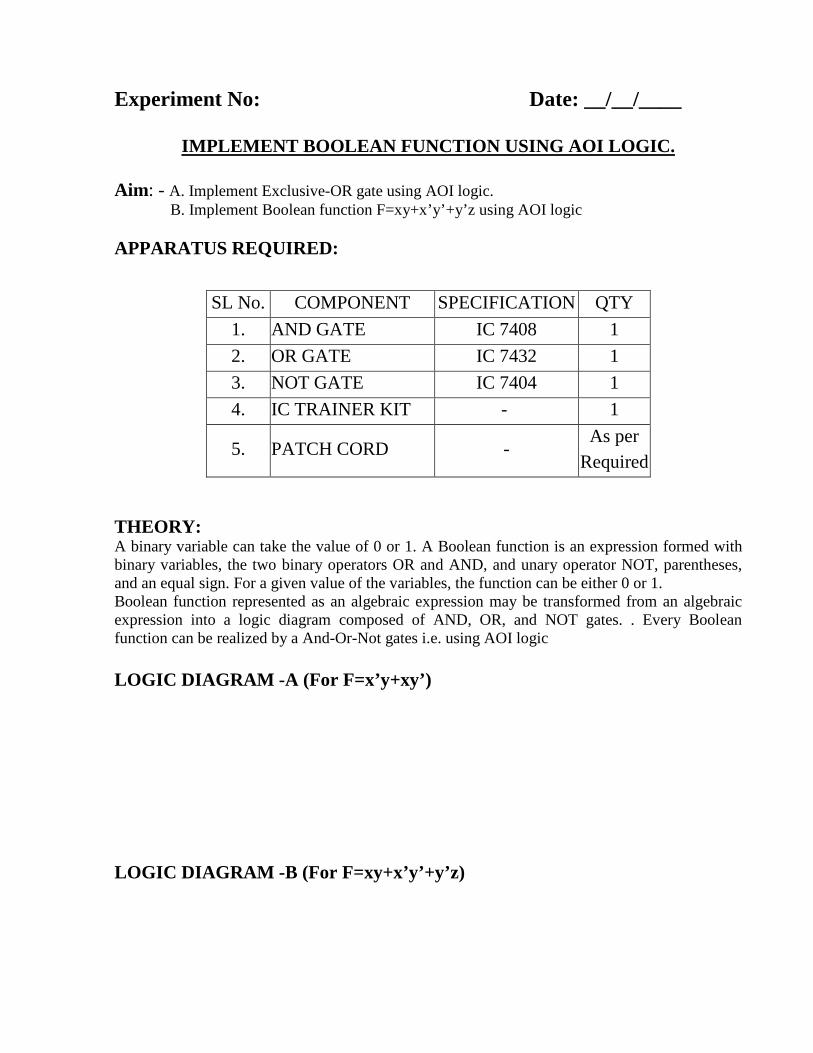
Experiment No: Date: __/__/____
STUDY OF LOGIC GATES AND VERIFY THEIR TRUTH TABLES. Aim: - Verification and interpretation of truth tables for AND, OR, NOT, NAND, NOR
Exclusive OR (EX-OR), Exclusive NOR (EX-NOR) Gates. APPARATUS REQUIRED:
THEORY: Logic gates are electronic circuits which perform logical functions on one or more inputs to produce one output. There are seven logic gates. When all the input combinations of a logic gate are written in a series and their corresponding outputs written along them, then this input/ output combination is called Truth Table. OR, AND and NOT are basic gates. NAND, NOR are known as universal gates. Various gates and their working is explained here. AND GATE: The AND gate performs a logical multiplication commonly known as AND function. The output is high when both the inputs are high. The output is low level when any one of the inputs is low.
OR GATE: The OR gate performs a logical addition commonly known as OR function. The output is high when any one of the inputs is high. The output is low level when both the inputs are low. NOT GATE: The NOT gate is called an inverter. The output is high when the input is low. The output is low when the input is high.
SL No. COMPONENT SPECIFICATION QTY 1. AND GATE IC 7408 1 2. OR GATE IC 7432 1 3. NOT GATE IC 7404 1 4. NAND GATE 2 I/P IC 7400 1 5. NOR GATE IC 7402 1 6. X-OR GATE IC 7486 1 7. IC TRAINER KIT - 1
8. PATCH CORD - As per
Required

NAND GATE: The NAND gate is a contraction of AND-NOT. The output is high when both inputs are low and any one of the input is low .The output is low level when both inputs are high. NOR GATE: The NOR gate is a contraction of OR-NOT. The output is high when both inputs are low. The output is low when one or both inputs are high.
X-OR GATE: The output is high when any one of the inputs is high. The output is low when both the inputs are low and both the inputs are high. PROCEDURE:
1. Connect the trainer kit to ac power supply. 2. Connect the inputs of any one logic gate to the logic sources and its output to the logic
indicator. 3. Apply various input combinations and observe output for each one. 4. Verify the truth table for each input/ output combination. 5. Repeat the process for all other logic gates. 6. Switch off the ac power supply.
GA
TE
SYMBOL FUNCTION OBSERVATION TRUTH TABLE
AN
D
OR

NO
T
NA
ND
NO
R
EX
-OR
EX
-NO
R
CONCLUSION:
Experiment No: Date: __/__/____
IMPLEMENT BOOLEAN FUNCTION USING AOI LOGIC. Aim: - A. Implement Exclusive-OR gate using AOI logic. B. Implement Boolean function F=xy+x’y’+y’z using AOI logic APPARATUS REQUIRED:
THEORY: A binary variable can take the value of 0 or 1. A Boolean function is an expression formed with binary variables, the two binary operators OR and AND, and unary operator NOT, parentheses, and an equal sign. For a given value of the variables, the function can be either 0 or 1. Boolean function represented as an algebraic expression may be transformed from an algebraic expression into a logic diagram composed of AND, OR, and NOT gates. . Every Boolean function can be realized by a And-Or-Not gates i.e. using AOI logic LOGIC DIAGRAM -A (For F=x’y+xy’) LOGIC DIAGRAM -B (For F=xy+x’y’+y’z)
SL No. COMPONENT SPECIFICATION QTY 1. AND GATE IC 7408 1 2. OR GATE IC 7432 1 3. NOT GATE IC 7404 1 4. IC TRAINER KIT - 1
5. PATCH CORD - As per
Required

PROCEDURE:
1. Connect the trainer kit to ac power supply. 2. Verify the gates and make connections as per circuit diagram-A. 3. Apply various input combinations and observe output for each one. 4. Verify the truth table for each input/ output combination. 5. Repeat the process for circuit diagram-B. 6. Switch off the ac power supply.
TRUTH TABLE: FOR A
FOR B
INPUT OUTPUT
x y z F
CONCLUSION:
INPUT OUTPUT x y F
Experiment No: Date: __/__/____
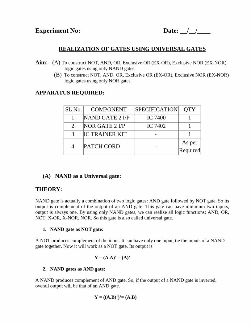
REALIZATION OF GATES USING UNIVERSAL GATES Aim: - (A) To construct NOT, AND, OR, Exclusive OR (EX-OR), Exclusive NOR (EX-NOR)
logic gates using only NAND gates. (B) To construct NOT, AND, OR, Exclusive OR (EX-OR), Exclusive NOR (EX-NOR)
logic gates using only NOR gates. APPARATUS REQUIRED:
(A) NAND as a Universal gate:
THEORY: NAND gate is actually a combination of two logic gates: AND gate followed by NOT gate. So its output is complement of the output of an AND gate. This gate can have minimum two inputs, output is always one. By using only NAND gates, we can realize all logic functions: AND, OR, NOT, X-OR, X-NOR, NOR. So this gate is also called universal gate.
1. NAND gate as NOT gate:
A NOT produces complement of the input. It can have only one input, tie the inputs of a NAND gate together. Now it will work as a NOT gate. Its output is
Y = (A.A)’ = (A)’
2. NAND gates as AND gate:
A NAND produces complement of AND gate. So, if the output of a NAND gate is inverted, overall output will be that of an AND gate. Y = ((A.B)’)’= (A.B)
SL No. COMPONENT SPECIFICATION QTY 1. NAND GATE 2 I/P IC 7400 1 2. NOR GATE 2 I/P IC 7402 1 3. IC TRAINER KIT - 1
4. PATCH CORD - As per
Required

3. NAND gates as OR gate:
From DeMorgan’s theorems: (A.B)’ = A’ + B’. Similarly, (A’.B’)’ = A’’ + B’’ = A + B So, give the inverted inputs to a NAND gate, obtain OR operation at output.
4. NAND gates as EX-OR gate:
The output of a two input EX-OR gate is given by: Y = A’B + AB’. EX-OR gate can be implemented using four NAND gates as follows. Gate No. Inputs Output 1 A, B (AB)’ 2 A, (AB)’ (A (AB)’)’ 3 (AB)’, B (B (AB)’)’ 4 (A (AB)’)’, (B (AB)’)’ A’B + AB’ Now the ouput from gate no. 4 is the overall output of the configuration.
Y = ((A (AB)’)’ (B (AB)’)’)’ = (A(AB)’)’’ + (B(AB)’)’’ = (A(AB)’) + (B(AB)’) = (A(A’ + B)’) + (B(A’ + B’))
= (AA’ + AB’) + (BA’ + BB’) = ( 0 + AB’ + BA’ + 0 ) = AB’ + BA’
So Y = AB’ + A’B
5. NAND gates as EX-NOR gate EX-NOR gate is actually EX-OR gate followed by NOT gate. So give the output of EX-OR gate to a NOT gate, overall ouput is that of an EX-NOR gate. Y = AB+ A’B’ PROCEDURE:
(i) Verify the gates and connect the NAND gates as per logic diagrams (A) for any of the logic functions to be realised.
(ii) Connect Pin-14 of all ICs to +5V and Pin-7 to ground. (iii) Feed the logic 0 (0V) or 1(5V) in different combinations at the inputs A & B
according to truth table. (iv) Observe and note down the output readings for Y for different combinations of
inputs and verify the truth table for input/output combination (v) Repeat the process for all logic functions/gates.
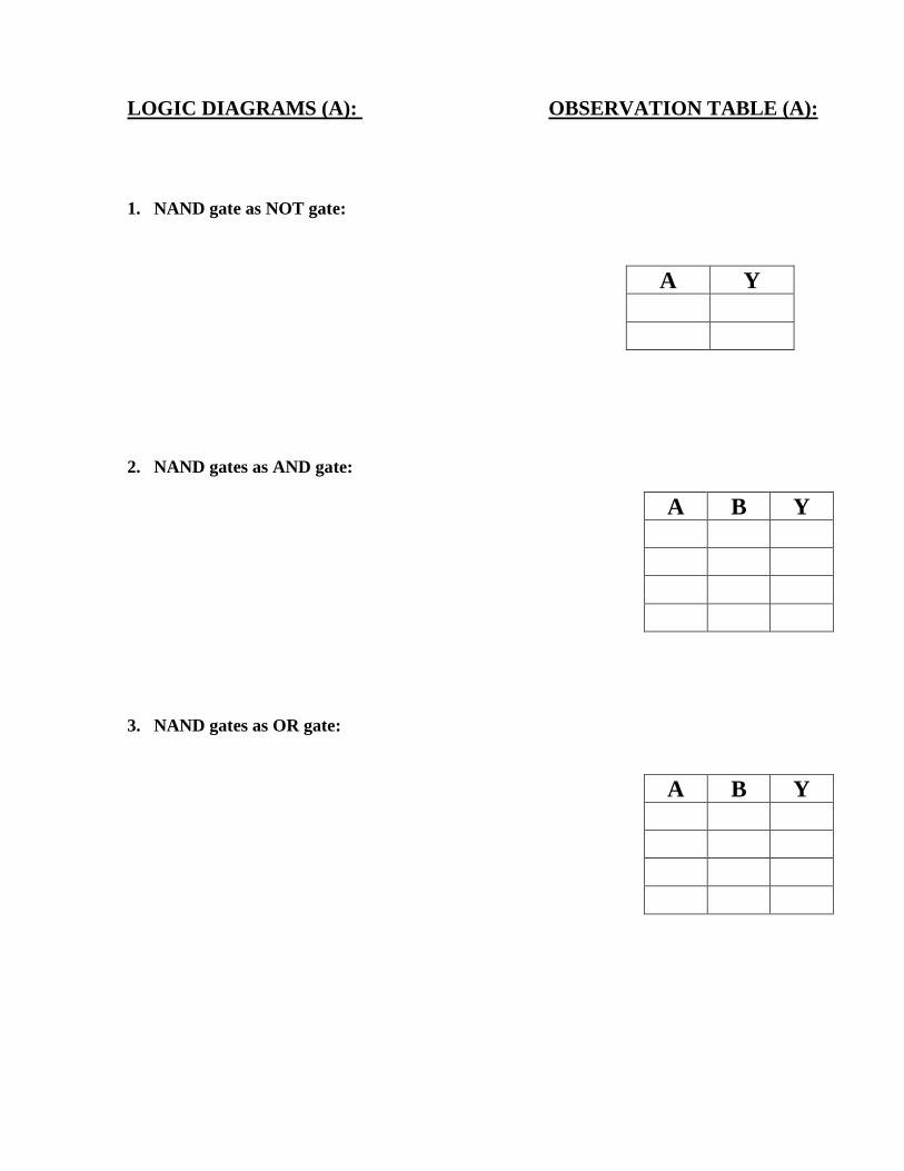
LOGIC DIAGRAMS (A): OBSERVATION TABLE (A): 1. NAND gate as NOT gate:
2. NAND gates as AND gate:
3. NAND gates as OR gate:
A Y
A B Y
A B Y
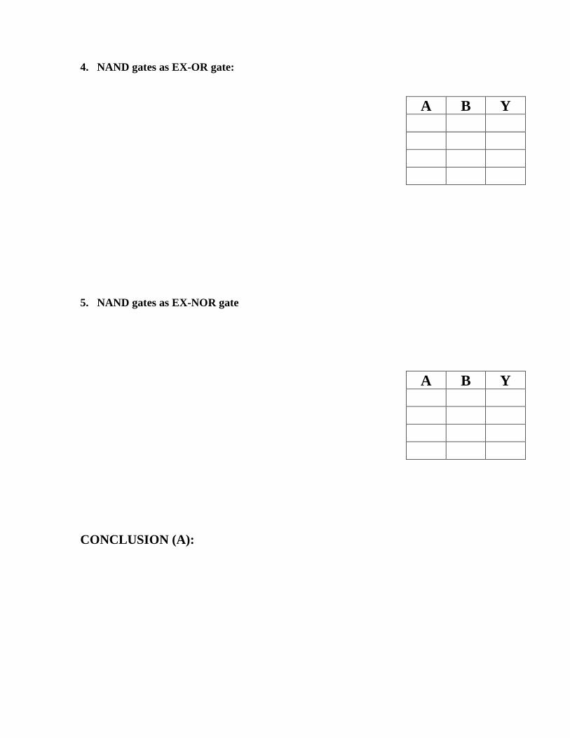
4. NAND gates as EX-OR gate:
5. NAND gates as EX-NOR gate CONCLUSION (A):
A B Y
A B Y
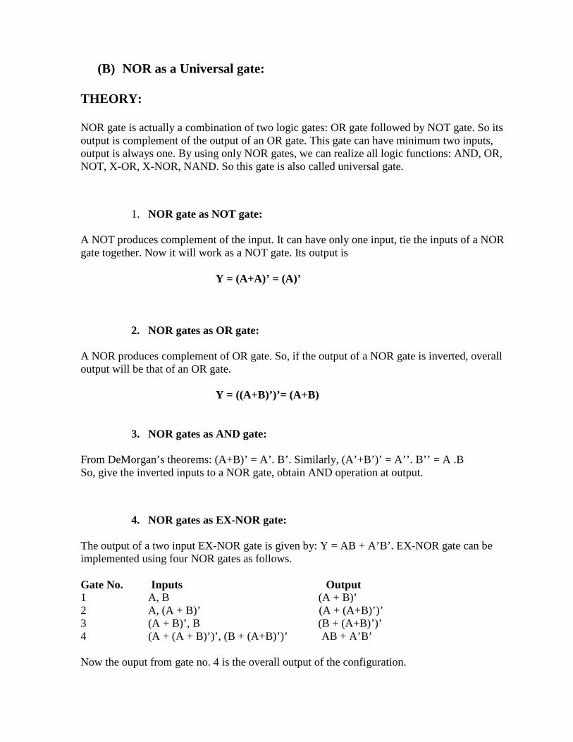
(B) NOR as a Universal gate:
THEORY: NOR gate is actually a combination of two logic gates: OR gate followed by NOT gate. So its output is complement of the output of an OR gate. This gate can have minimum two inputs, output is always one. By using only NOR gates, we can realize all logic functions: AND, OR, NOT, X-OR, X-NOR, NAND. So this gate is also called universal gate.
1. NOR gate as NOT gate:
A NOT produces complement of the input. It can have only one input, tie the inputs of a NOR gate together. Now it will work as a NOT gate. Its output is
Y = (A+A)’ = (A)’
2. NOR gates as OR gate:
A NOR produces complement of OR gate. So, if the output of a NOR gate is inverted, overall output will be that of an OR gate. Y = ((A+B)’)’= (A+B)
3. NOR gates as AND gate:
From DeMorgan’s theorems: (A+B)’ = A’. B’. Similarly, (A’+B’)’ = A’’. B’’ = A .B So, give the inverted inputs to a NOR gate, obtain AND operation at output.
4. NOR gates as EX-NOR gate:
The output of a two input EX-NOR gate is given by: Y = AB + A’B’. EX-NOR gate can be implemented using four NOR gates as follows. Gate No. Inputs Output 1 A, B (A + B)’ 2 A, (A + B)’ (A + (A+B)’)’ 3 (A + B)’, B (B + (A+B)’)’ 4 (A + (A + B)’)’, (B + (A+B)’)’ AB + A’B’ Now the ouput from gate no. 4 is the overall output of the configuration.
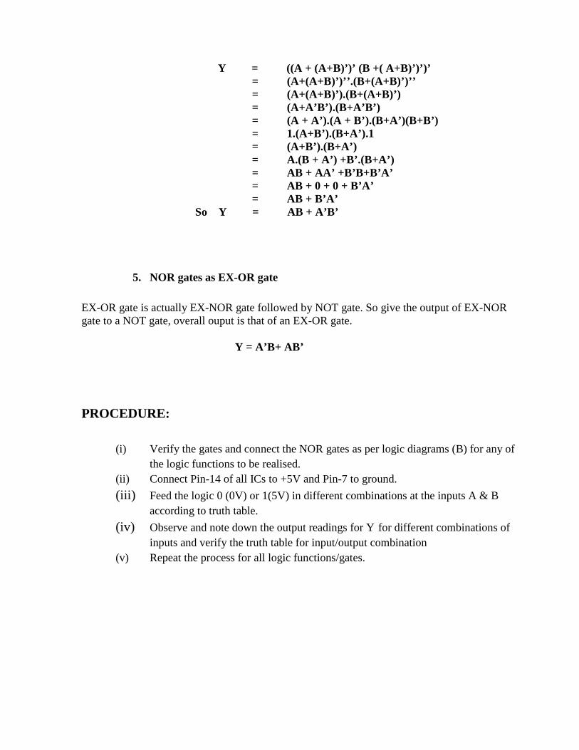
Y = ((A + (A+B)’)’ (B +( A+B)’)’)’ = (A+(A+B)’)’’.(B+(A+B)’)’’ = (A+(A+B)’).(B+(A+B)’) = (A+A’B’).(B+A’B’)
= (A + A’).(A + B’).(B+A’)(B+B’) = 1.(A+B’).(B+A’).1 = (A+B’).(B+A’)
= A.(B + A’) +B’.(B+A’) = AB + AA’ +B’B+B’A’ = AB + 0 + 0 + B’A’ = AB + B’A’ So Y = AB + A’B’
5. NOR gates as EX-OR gate EX-OR gate is actually EX-NOR gate followed by NOT gate. So give the output of EX-NOR gate to a NOT gate, overall ouput is that of an EX-OR gate. Y = A’B+ AB’ PROCEDURE:
(i) Verify the gates and connect the NOR gates as per logic diagrams (B) for any of the logic functions to be realised.
(ii) Connect Pin-14 of all ICs to +5V and Pin-7 to ground. (iii) Feed the logic 0 (0V) or 1(5V) in different combinations at the inputs A & B
according to truth table. (iv) Observe and note down the output readings for Y for different combinations of
inputs and verify the truth table for input/output combination (v) Repeat the process for all logic functions/gates.
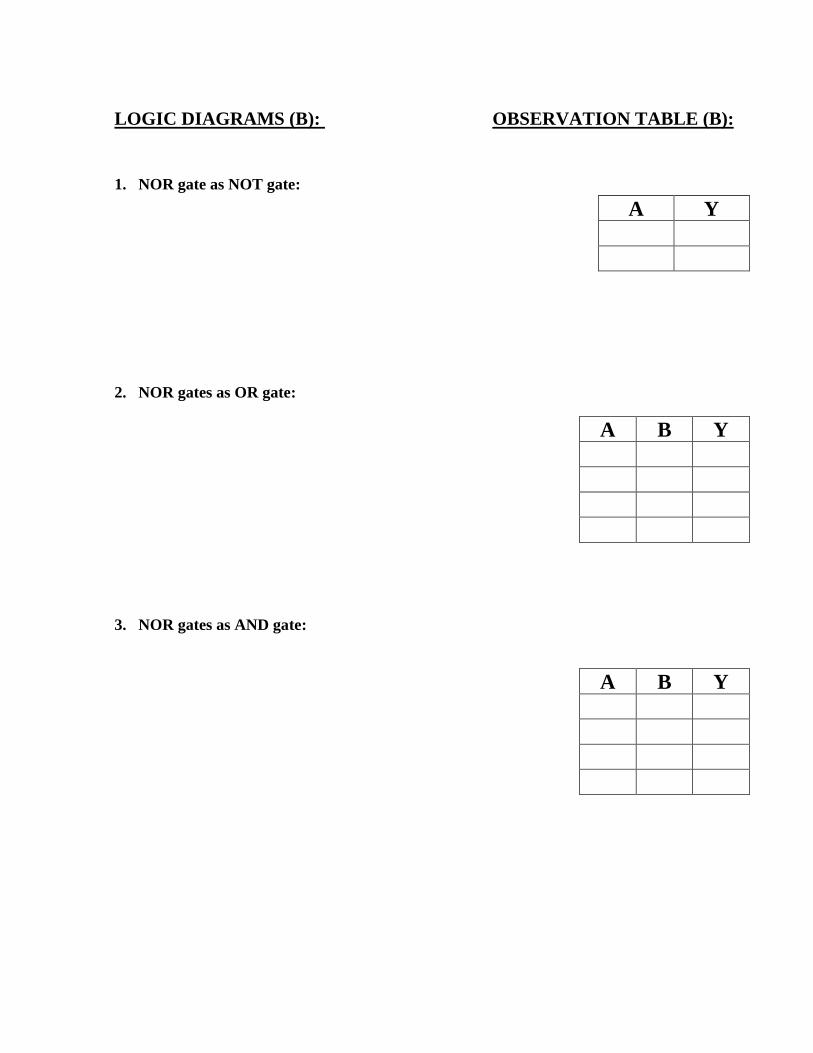
LOGIC DIAGRAMS (B): OBSERVATION TABLE (B): 1. NOR gate as NOT gate:
2. NOR gates as OR gate:
3. NOR gates as AND gate:
A Y
A B Y
A B Y

4. NOR gates as EX-NOR gate:
5. NOR gates as EX-OR gate CONCLUSION (B) :
A B Y
A B Y

Experiment No: Date: __/__/____
VERIFICATION OF K-MAP. Aim: - Simplify the Boolean function F(w, x, y, z) = Σ (0, 1,2,4,5,6,8,9, 12, 13, 14) using 4-
variable K-Map, implement it and verify it using truth-table. APPARATUS REQUIRED:
THEORY: The complexity of the digital logic gates that implement a Boolean function is directly related to the complexity of the algebraic expression from which the function is implemented. Although the truth table representation of a function is unique, expressed algebraically, it can appear in many different forms. Boolean functions may be simplified by algebraic means. However, this procedure of minimization is awkward because it lacks specific rules to predict each succeeding step in the manipulative process. The map method provides a simple straightforward procedure for minimizing Boolean functions. This method may be regarded either as a pictorial form of a truth table or as an extension of the Venn diagram. The map method, first proposed by Veitch and modified by Karnaugh, is also known as the "Veitch diagram" or the "Karnaugh map." The map is a diagram made up of squares. Each square represents one minterm. Since any Boolean function can be expressed as a sl1m of minterms, it follows that a Boolean function is recognized graphically in the map from the area enclosed by those squares whose min terms are included in the function. In fact, the map presents a visual diagram of all possible ways a function may be expressed in a standard form. By recognizing various patterns, the user can derive alternative algebraic expressions for the same function, from which he can select the simplest one. We shall assume that the simplest algebraic expression is anyone in a sum of products or product of sums that has a minimum number of literals. (This expression is not necessarily unique.) The map for Boolean functions of four binary variables has 16 minterms and the square is assigned to each. The rows and columns are numbered in a reflected-code sequence, with only one digit changing value between two adjacent rows or columns. The minterm corresponding to each square can be obtained from the concatenation of the row number with the column number. For example, the numbers of the third row (11) and the second column (01), when concatenated,
SL No. COMPONENT SPECIFICATION QTY 1. AND GATE IC 7408 1 2. OR GATE IC 7432 1 3. NOT GATE IC 7404 1 4. NAND GATE 2 I/P IC 7400 1 5. NOR GATE IC 7402 1 6. X-OR GATE IC 7486 1 7. IC TRAINER KIT - 1
8. PATCH CORD - As per
Required
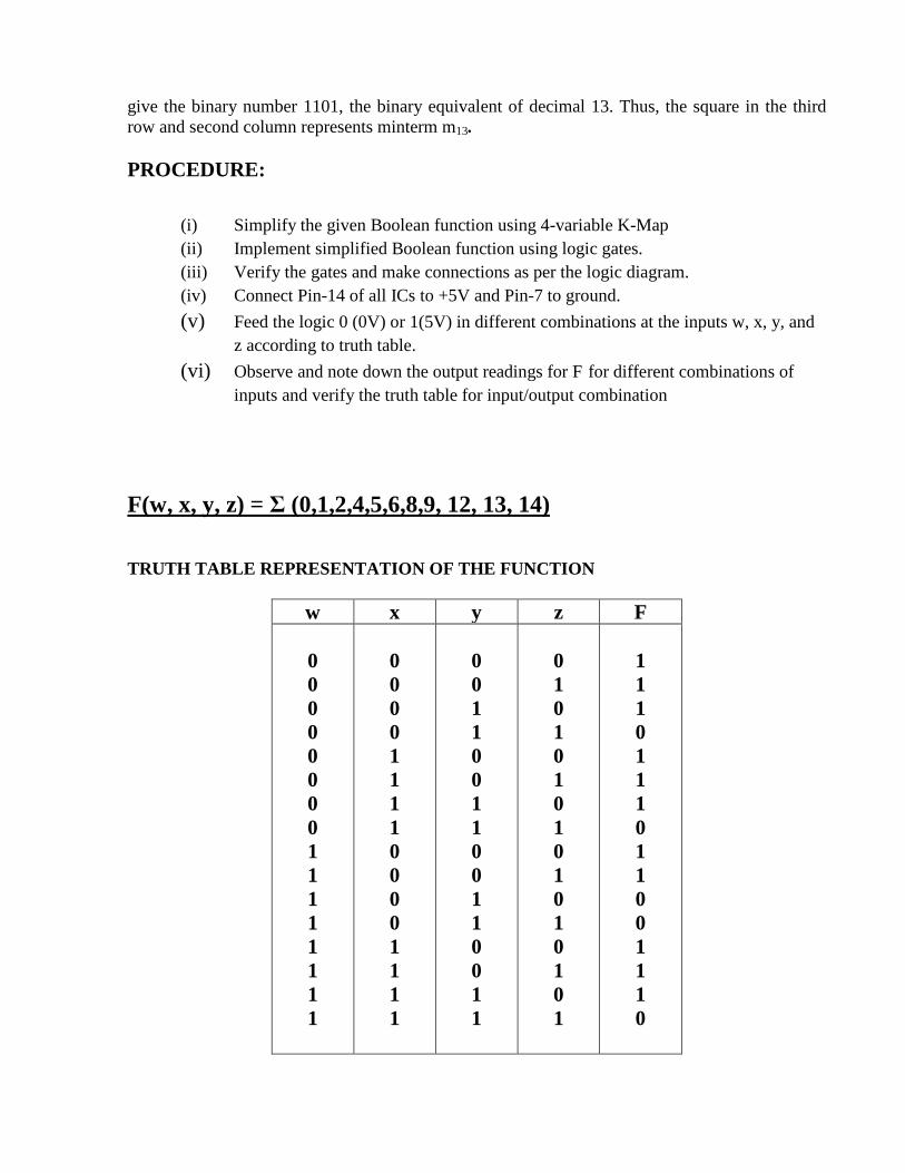
give the binary number 1101, the binary equivalent of decimal 13. Thus, the square in the third row and second column represents minterm m13. PROCEDURE:
(i) Simplify the given Boolean function using 4-variable K-Map (ii) Implement simplified Boolean function using logic gates. (iii) Verify the gates and make connections as per the logic diagram. (iv) Connect Pin-14 of all ICs to +5V and Pin-7 to ground. (v) Feed the logic 0 (0V) or 1(5V) in different combinations at the inputs w, x, y, and
z according to truth table. (vi) Observe and note down the output readings for F for different combinations of
inputs and verify the truth table for input/output combination F(w, x, y, z) = Σ (0,1,2,4,5,6,8,9, 12, 13, 14) TRUTH TABLE REPRESENTATION OF THE FUNCTION
w x y z F 0 0 0 0 0 0 0 0 1 1 1 1 1 1 1 1
0 0 0 0 1 1 1 1 0 0 0 0 1 1 1 1
0 0 1 1 0 0 1 1 0 0 1 1 0 0 1 1
0 1 0 1 0 1 0 1 0 1 0 1 0 1 0 1
1 1 1 0 1 1 1 0 1 1 0 0 1 1 1 0

SIMPLIFICATION USING 4-VARIABLE K-MAP
Simplified Boolean function F=_______________________
LOGIC DIAGRAM OF SIMPLIFIED BOOLEAN FUNCTION
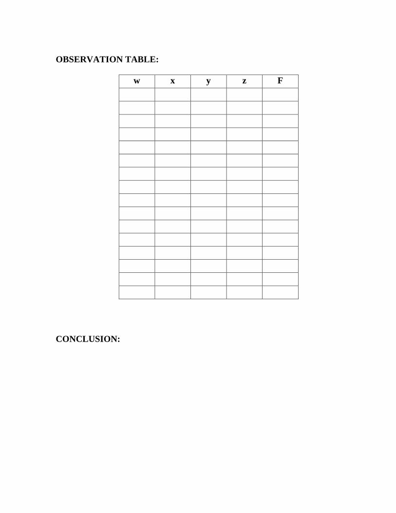
OBSERVATION TABLE:
w x y z F
CONCLUSION:
Experiment No: Date: __/__/____
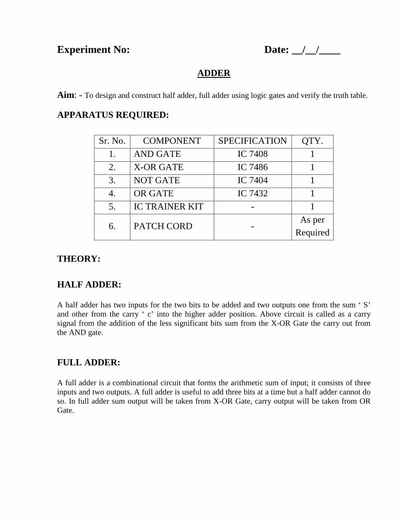
ADDER Aim: - To design and construct half adder, full adder using logic gates and verify the truth table. APPARATUS REQUIRED:
Sr. No. COMPONENT SPECIFICATION QTY. 1. AND GATE IC 7408 1 2. X-OR GATE IC 7486 1 3. NOT GATE IC 7404 1 4. OR GATE IC 7432 1 5. IC TRAINER KIT - 1
6. PATCH CORD - As per
Required THEORY: HALF ADDER:
A half adder has two inputs for the two bits to be added and two outputs one from the sum ‘ S’ and other from the carry ‘ c’ into the higher adder position. Above circuit is called as a carry signal from the addition of the less significant bits sum from the X-OR Gate the carry out from the AND gate. FULL ADDER:
A full adder is a combinational circuit that forms the arithmetic sum of input; it consists of three inputs and two outputs. A full adder is useful to add three bits at a time but a half adder cannot do so. In full adder sum output will be taken from X-OR Gate, carry output will be taken from OR Gate.
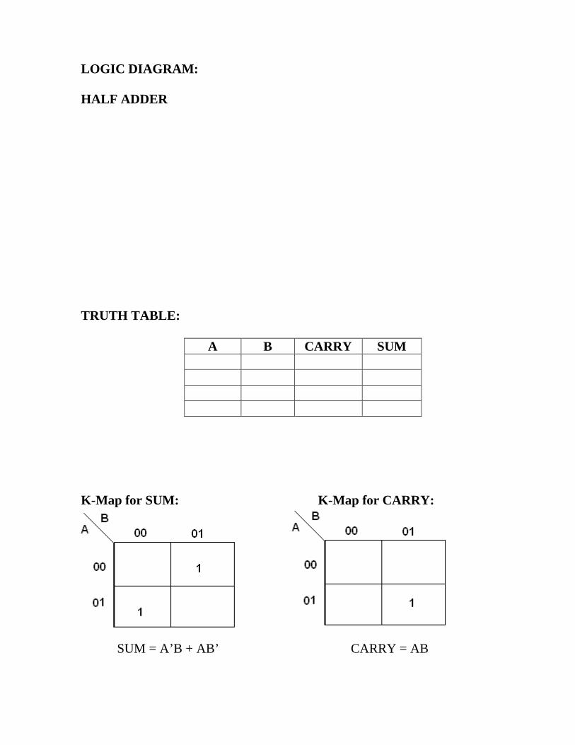
LOGIC DIAGRAM: HALF ADDER
TRUTH TABLE:
A B CARRY SUM
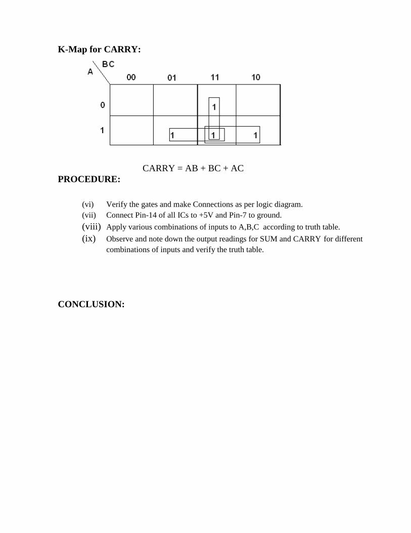
K-Map for SUM: K-Map for CARRY:
SUM = A’B + AB’ CARRY = AB
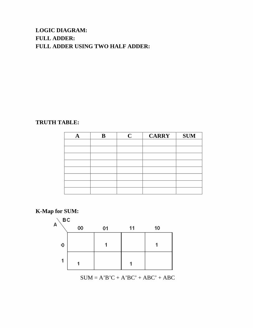
LOGIC DIAGRAM: FULL ADDER: FULL ADDER USING TWO HALF ADDER: TRUTH TABLE:
A B C CARRY SUM
K-Map for SUM:
SUM = A’B’C + A’BC’ + ABC’ + ABC
K-Map for CARRY:
CARRY = AB + BC + AC PROCEDURE:
(vi) Verify the gates and make Connections as per logic diagram. (vii) Connect Pin-14 of all ICs to +5V and Pin-7 to ground. (viii) Apply various combinations of inputs to A,B,C according to truth table. (ix) Observe and note down the output readings for SUM and CARRY for different
combinations of inputs and verify the truth table.
CONCLUSION:

Experiment No: Date: __/__/____
SUBTRACTOR
AIM: To design and construct half subtractor and full subtractor circuits using logic gates and verify the truth table.
APPARATUS REQUIRED:
Sr. No. COMPONENT SPECIFICATION QTY. 1. AND GATE IC 7408 1 2. X-OR GATE IC 7486 1 3. NOT GATE IC 7404 1 4. OR GATE IC 7432 1 5. IC TRAINER KIT - 1
6. PATCH CORD - As per
Required THEORY: HALF SUBTRACTOR:
The half subtractor is constructed using X-OR and AND Gate. The half subtractor has two input and two outputs. The outputs are difference and borrow. The difference can be applied using X-OR Gate, borrow output can be implemented using an AND Gate and an inverter. FULL SUBTRACTOR:
The full subtractor is a combination of X-OR, AND, OR, NOT Gates. In a full subtractor the logic circuit should have three inputs and two outputs. The two half subtractor put together gives a full subtractor .The first half subtractor will be C and A B. The output will be difference output of full subtractor. The expression AB assembles the borrow output of the half subtractor and the second term is the inverted difference output of first X-OR.

LOGIC DIAGRAM: HALF SUBTRACTOR
TRUTH TABLE:
A B BORROW DIFFERENCE
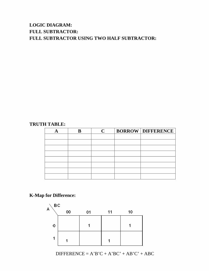
K-Map for DIFFERENCE:
DIFFERENCE = A’B + AB’ K-Map for BORROW:
BORROW = A’B
LOGIC DIAGRAM: FULL SUBTRACTOR: FULL SUBTRACTOR USING TWO HALF SUBTRACTOR: TRUTH TABLE:
A B C BORROW DIFFERENCE
K-Map for Difference:
DIFFERENCE = A’B’C + A’BC’ + AB’C’ + ABC

K-Map for Borrow:
BORROW = A’B + BC + A’C PROCEDURE:
(i) Verify the gates and make connections as per logic diagram. (ii) Connect Pin-14 of all ICs to +5V and Pin-7 to ground. (iii) Apply various combinations of inputs to A,B,C according to truth table. (iv) Observe and note down the output readings for SUM and CARRY for different
combinations of inputs and verify the truth table.
CONCLUSION:
Experiment No: Date: __/__/____
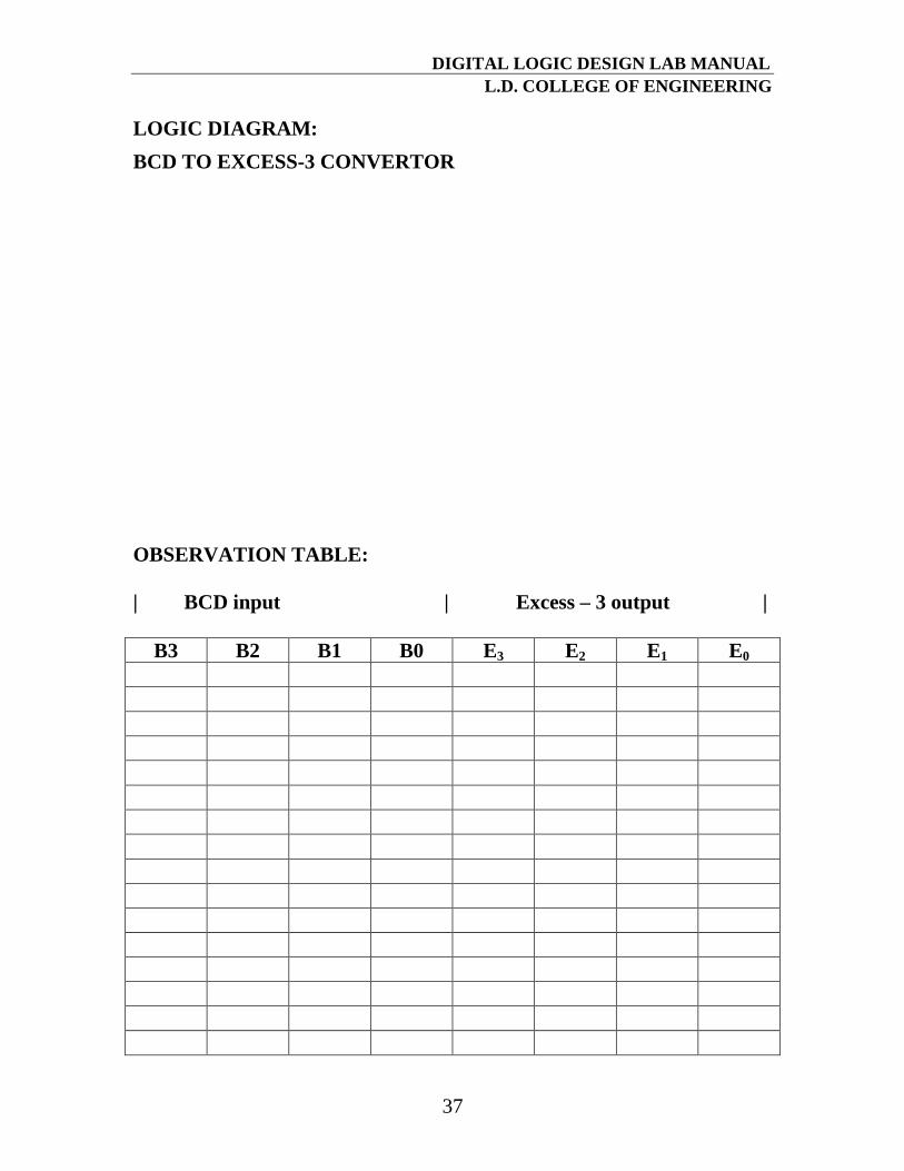
BCD TO EXCESS-3 CODE CONVERTER
AIM: To Design and Implement BCD TO EXCESS-3 CONVERTER and verify the truth table APPARATUS REQUIRED:
Sr. No. COMPONENT SPECIFICATION QTY.
1. AND GATE IC 7408 1 2. X-OR GATE IC 7486 1 3. NOT GATE IC 7404 1 4. OR GATE IC 7432 1 5. IC TRAINER KIT - 1
6. PATCH CORD - As per
Required THEORY:
The availability of large variety of codes for the same discrete elements of information results in the use of different codes by different systems. A conversion circuit must be inserted between the two systems if each uses different codes for same information. Thus, code converter is a circuit that makes the two systems compatible even though each uses different binary code. Binary Coded Decimal: Binary Coded Decimal is a method of using binary digits to represent the decimal digits 0 through 9. It is possible to assign weights to the binary bits according to their positions. The weights in the BCD code are 8, 4, 2 and 1. Ex: (137)10 - BCD equivalent (0001 0011 0111)2. Excess-3 Code: This is an un-weighted code. Its code assignment is obtained from the corresponding value of BCD after the addition of (0011)2.
BCD to Excess-3 (or) Excess-3 to BCD: Since each code uses four bits to represent a decimal digit, there must be four inputs and four output variables. The input variable are designated as B3, B2, B1, B0 and the output variables are designated as E3, E2, E1, E0 in the truth table. Four binary variables have sixteen different input combinations, only ten of the input combinations are listed in the truth table. The six bit combinations not listed for the input variables are don’t care combination. The Boolean functions are obtained from K-Map for each output variable. The combinational logic for t h e code converters are designed according the Boolean expressions from K -Map

simplification. The Boolean expressions from the K-Map are shown below. Each one of the four maps represents one of the four outputs of the circuit as a function of the four input variables. A two-level logic diagram may be obtained directly from the Boolean expressions derived by the maps. These are various other possibilities for a logic diagram that implements this circuit. PROCEDURE:
(i) Determine number of available input variables and required output variables and assign letter symbols to them.
(ii) Derive appropriate truth table. (iii) Obtain simplified Boolean function for each output variable. (iv) Draw logic diagram. (v) Verify the gates. (vi) Make connections as per the logic diagram. (vii) Connect Pin-14 of all ICs to +5V and Pin-7 to ground. (viii) Apply various combinations of inputs to B3, B2, B1, B0 for BCD according to
truth table. (ix) Observe and note down the output readings for E3, E2, E1, E0 for different
combinations of inputs for corresponding Excess-3. (x) Verify the truth table.
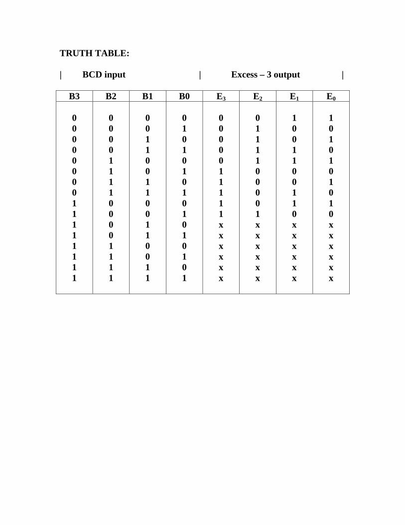
TRUTH TABLE: | BCD input | Excess – 3 output |
B3 B2 B1 B0 E3 E2 E1 E0 0 0 0 0 0 0 0 0 1 1 1 1 1 1 1 1
0 0 0 0 1 1 1 1 0 0 0 0 1 1 1 1
0 0 1 1 0 0 1 1 0 0 1 1 0 0 1 1
0 1 0 1 0 1 0 1 0 1 0 1 0 1 0 1
0 0 0 0 0 1 1 1 1 1 x x x x x x
0 1 1 1 1 0 0 0 0 1 x x x x x x
1 0 0 1 1 0 0 1 1 0 x x x x x x
1 0 1 0 1 0 1 0 1 0 x x x x x x
DIGITAL LOGIC DESIGN LAB MANUAL L.D. COLLEGE OF ENGINEERING
35
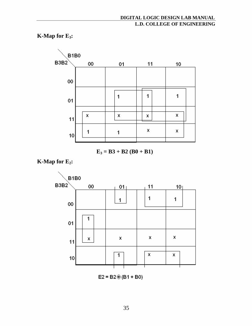
K-Map for E3:
E3 = B3 + B2 (B0 + B1)
K-Map for E2:
DIGITAL LOGIC DESIGN LAB MANUAL L.D. COLLEGE OF ENGINEERING
36
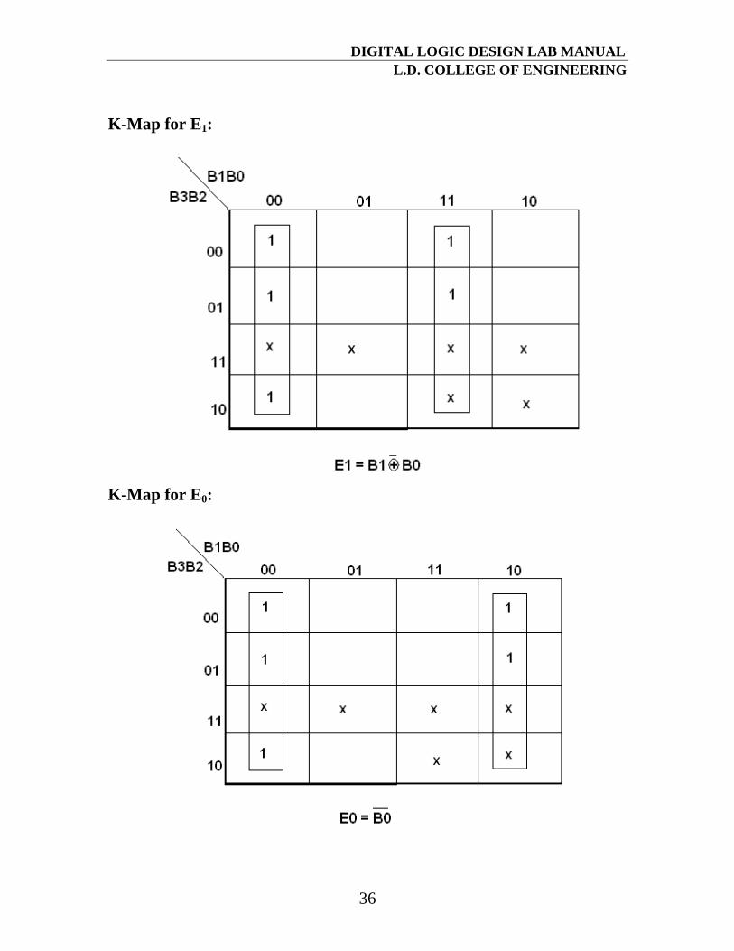
K-Map for E1:
K-Map for E0:
DIGITAL LOGIC DESIGN LAB MANUAL L.D. COLLEGE OF ENGINEERING
37
LOGIC DIAGRAM: BCD TO EXCESS-3 CONVERTOR
OBSERVATION TABLE: | BCD input | Excess – 3 output |
B3 B2 B1 B0 E3 E2 E1 E0

DIGITAL LOGIC DESIGN LAB MANUAL L.D. COLLEGE OF ENGINEERING
38
CONCLUSION:
DIGITAL LOGIC DESIGN LAB MANUAL L.D. COLLEGE OF ENGINEERING
39
Experiment No: Date: __/__/____
BINARY TO GRAY /GRAY TO BINARY CODE CONVERTER
AIM: To Design & implement 4-bit Binary to gray code converter/ 4-bit Gray to Binary code converter and verify the truth table.
APPARATUS REQUIRED:
Sr. No. COMPONENT SPECIFICATION QTY.
1. X-OR GATE IC 7486 1 2. IC TRAINER KIT - 1
3. PATCH CORD - As per
Required THEORY: Gray Code: To obtain a different gray code, one can start with any bit information and proceed to obtain the next bit combination by changing only one bit from 0 to 1 (or) 1 to 0 in any desired random fashion provided any two numbers do not have identical code assignments. Binary to Gray (or) Gray to Binary conversion: To convert from binary code to Gray code, the input lines must supply the bit combination of elements as specified by the code and the output lines generate the corresponding bit combination of code. In the case of binary to gray conversion, the input variable are designated as B3, B2, B1, B0 and the output variables are designated as G3, G2, G1, G0. While in the case of gray to binary conversion, the input variable are designated as G3, G2, G1, G0 and the output variables are designated as B3, B2, B1, B0 in the truth table . Four binary variables have sixteen different input combinations. The Boolean functions are obtained from K-Map for each output variable. The combinational logic for t h e code converters are designed according the Boolean expressions from K -Map simplification. The Boolean expressions from the K-Map are shown below. Each one of the four maps represents one of the four outputs of the circuit as a function of the four input variables.
DIGITAL LOGIC DESIGN LAB MANUAL L.D. COLLEGE OF ENGINEERING
40
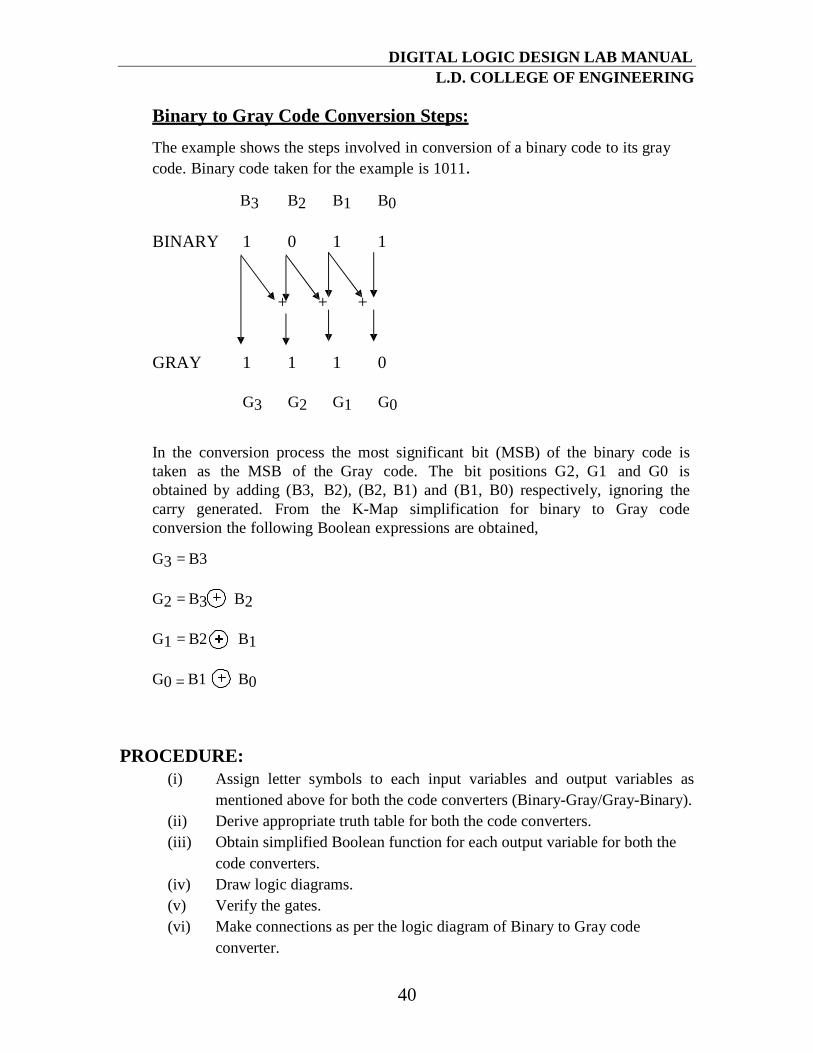
Binary to Gray Code Conversion Steps:
The example shows the steps involved in conversion of a binary code to its gray code. Binary code taken for the example is 1011.
B3 B2 B1 B0
BINARY
1
0
1
1
+ + +
GRAY 1 1 1 0
G3
G2
G1
G0
In the conversion process the most significant bit (MSB) of the binary code is taken as the MSB of the Gray code. The bit positions G2, G1 and G0 is obtained by adding (B3, B2), (B2, B1) and (B1, B0) respectively, ignoring the carry generated. From the K-Map simplification for binary to Gray code conversion the following Boolean expressions are obtained,
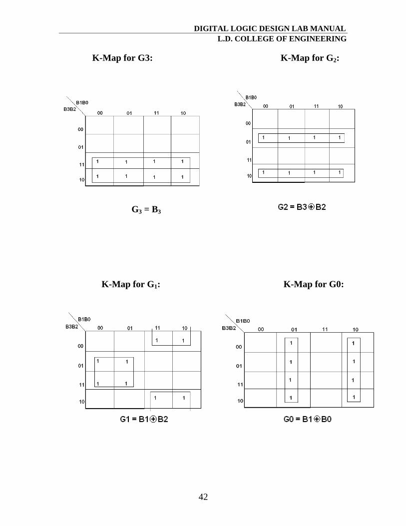
G3 = B3
G2 = B3 B2
G1 = B2 B1
G0 = B1 B0
PROCEDURE:
(i) Assign letter symbols to each input variables and output variables as mentioned above for both the code converters (Binary-Gray/Gray-Binary).
(ii) Derive appropriate truth table for both the code converters. (iii) Obtain simplified Boolean function for each output variable for both the
code converters. (iv) Draw logic diagrams. (v) Verify the gates. (vi) Make connections as per the logic diagram of Binary to Gray code
converter.

DIGITAL LOGIC DESIGN LAB MANUAL L.D. COLLEGE OF ENGINEERING
41
(vii) Connect Pin-14 of IC to +5V and Pin-7 to ground. (viii) Apply various combinations of inputs to B3, B2, B1, and B0 according to
truth table. (ix) Observe and note down the output readings for G3, G2, G1, and G0 for all
the 16 combinations of the inputs for corresponding Gray code. (x) Verify the truth table. (xi) Now make connections as per the logic diagram of Gray to Binary code
converter. (xii) Apply various combinations of inputs to G3, G2, G1, and G0 according to
truth table. (xiii) Observe and note down the output readings for B3, B2, B1, and B0 for all
the 16 combinations of the inputs for corresponding Binary code. (xiv) Verify the truth table.
BINARY TO GRAY CODE CONVERTOR TRUTH TABLE: | Binary input | Gray code output |
B3 B2 B1 B0 G3 G2 G1 G0 0 0 0 0 0 0 0 0 1 1 1 1 1 1 1 1
0 0 0 0 1 1 1 1 0 0 0 0 1 1 1 1
0 0 1 1 0 0 1 1 0 0 1 1 0 0 1 1
0 1 0 1 0 1 0 1 0 1 0 1 0 1 0 1
0 0 0 0 0 0 0 0 1 1 1 1 1 1 1 1
0 0 0 0 1 1 1 1 1 1 1 1 0 0 0 0
0 0 1 1 1 1 0 0 0 0 1 1 1 1 0 0
0 1 1 0 0 1 1 0 0 1 1 0 0 1 1 0
DIGITAL LOGIC DESIGN LAB MANUAL L.D. COLLEGE OF ENGINEERING
42
K-Map for G3: K-Map for G2:
G3 = B3 K-Map for G1: K-Map for G0:
DIGITAL LOGIC DESIGN LAB MANUAL L.D. COLLEGE OF ENGINEERING
43
LOGIC DIAGRAM:
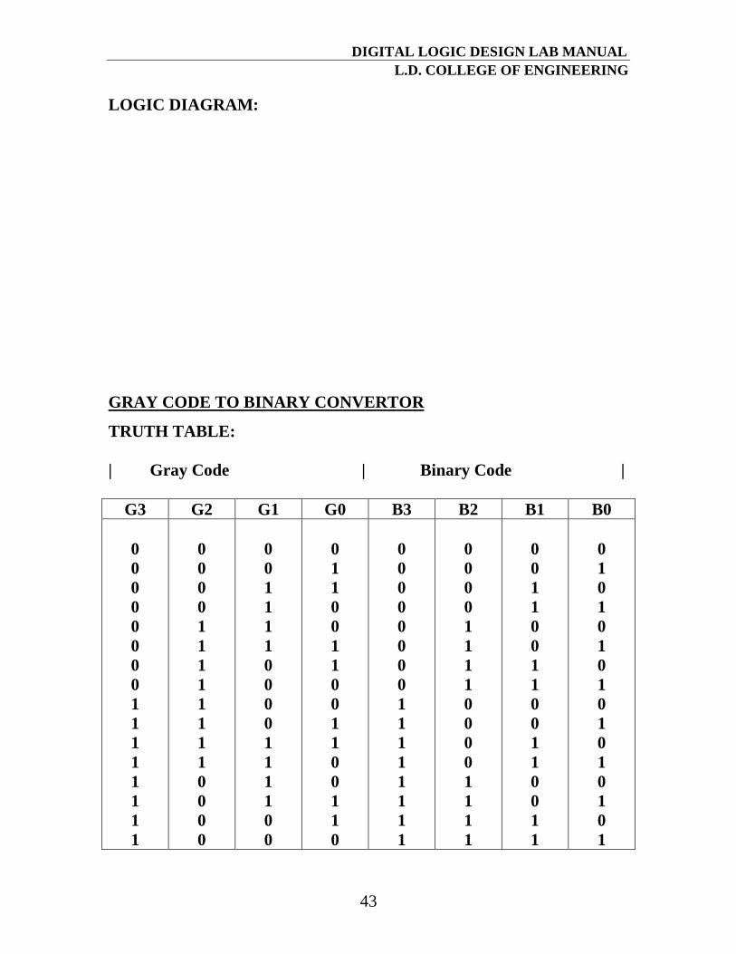
GRAY CODE TO BINARY CONVERTOR
TRUTH TABLE:
| Gray Code | Binary Code |
G3 G2 G1 G0 B3 B2 B1 B0 0 0 0 0 0 0 0 0 1 1 1 1 1 1 1 1
0 0 0 0 1 1 1 1 1 1 1 1 0 0 0 0
0 0 1 1 1 1 0 0 0 0 1 1 1 1 0 0
0 1 1 0 0 1 1 0 0 1 1 0 0 1 1 0
0 0 0 0 0 0 0 0 1 1 1 1 1 1 1 1
0 0 0 0 1 1 1 1 0 0 0 0 1 1 1 1
0 0 1 1 0 0 1 1 0 0 1 1 0 0 1 1
0 1 0 1 0 1 0 1 0 1 0 1 0 1 0 1
DIGITAL LOGIC DESIGN LAB MANUAL L.D. COLLEGE OF ENGINEERING
44
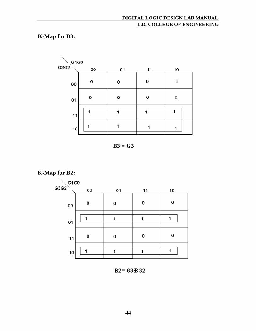
K-Map for B3:
B3 = G3
K-Map for B2:
DIGITAL LOGIC DESIGN LAB MANUAL L.D. COLLEGE OF ENGINEERING
45
K-Map for B1:
K-Map for B0:

DIGITAL LOGIC DESIGN LAB MANUAL L.D. COLLEGE OF ENGINEERING
46
LOGIC DIAGRAM:
DIGITAL LOGIC DESIGN LAB MANUAL L.D. COLLEGE OF ENGINEERING
47
OBSERVATION TABLE:
CONCLUSION:
G3 G2 G1 G0 B3 B2 B1 B0
G3 G2 G1 G0 B3 B2 B1 B0