lab 3 - tec
DESCRIPTION
electronics labTRANSCRIPT

LABORATORUL 3
TRANZISTORUL CU EFECT DE CAMP
The object of this module is to study the behavior of a field effect transistor in common source and common drain configurations and to highlight the differences between FETs and bipolar transistors.
Field Effect Transistors SO 4201-7J
Technical data:
Power requirements: +15V 0-10Vpp / 1kHz
Polarity protected,
Overvoltage protection up to 24 V
Dimensions: Euro-card 160x100 mm
Circuit groups: - Transistor circuit with single 2N 3819 field effect transistor
- 3 simulated faults
Description
This card contains a simple circuit incorporating an N-channel, depletion layer field effect transistor. The FET can be connected for common source or common drain operation. DC or AC feedback can be applied by inserting and removing jumpers. This simple circuit can be used for illustrating the advantages of FETs as compared to bipolar transistors (e.g. their use as impedance converters and HF pre-amp's).
The circuit features 3 simulated faults that can be separately activated.
Field effect transistors
Introduction
Study objectives:
Field effect transistor in common source configuration
Field effect transistor in common drain configuration
Differences and similarities to bipolar transistors

The earliest design of transistor consisted of a "sandwich" of N and P-doped silicon that involved two PN junctions. Nowadays, in many applications, this type of bipolar transistor has been replaced by newer types that contain only one PN junction. These components are called Field Effect Transistors or FETs. FETs are frequently cheaper and easier to manufacture than bipolars and their design lends itself to even greater miniaturisation. The overwhelming majority of transistors built into ICs and microprocessors are field effect types.
N-channel FET
The basic design of an FET involves a thin block of doped silicon. In the middle of the block, a region of oppositely doped material is produced. This can be achieved by introducing appropriate impurities at a single point and allowing them to diffuse into the silicon. An electrical connection is made to this region as well as two more, one at each end of the block. The connection to the oppositely doped region in the middle is called the gate and those at either end are called the source and the drain. The size of the doped region at the gate is so controlled that a narrow channel of silicon with the original doping is left. If the original doping of the silicon was N-type, the gate will be P-type and a narrow channel of N-type material will be left. Such components are therefore called n-channel FETs. The corresponding design using P-type material with an N-type gate is called a p-channel FET. N-channel FETs tend to be used more often than p-channel types. This is because their majority charge carriers are electrons which are more mobile than the holes that are the principle carriers in a P-channel FET. This means that n-channel FETs are usually faster than their P-type equivalents.
The n-channel FET is usually operated with the gate at a more negative voltage than the source. This means that the PN junction in the FET is reverse-biased. The transistor effect is produced by the depletion layer that forms at the reverse-biased junction. A depletion layer is caused by electrons from the N-type material combining with holes in the P-type material along the surface of the junction. It results in a relative lack of majority charge carriers on each side of the junction. The N-type material near the junction is depleted of electrons and the P-type material is depleted of holes.
Now when a voltage is applied across the junction to make it reverse-biased, the minority carriers, electrons in the P-type material and holes in the N-type material, are drawn towards the junction so that there is more recombination in the vicinity of junction and the depletion layer becomes wider.
In the FET, any increase in the size of the depletion layer has the effect of narrowing the conducting channel. The depletion layer itself is less conductive because there are relatively fewer available charge carriers. The result is that the increase in the size of the depletion layer caused by the gate becoming more negative results in constriction of the channel and less current flowing between drain and source. Similarly as the gate becomes more positive the depletion layer shrinks, the channel becomes wider and more current

flows between drain and source. Small variations in gate voltage may lead to quite large variations in drain-source current and thus to the voltage at the drain itself. Therefore, the FET acts as a current and voltage amplifier in the same way as a bipolar transistor (see Basic Transistor Circuits SO4203-7E).
As with bipolar transistors, there are standard configurations for an amplifier circuit using FETs. The two most basic are the common source circuit, which is analogous to a bipolar transistor's common emitter configuration, and the common drain which resembles a common collector circuit in many respects. Both these two configurations are investigated in the following experiments.
The illustration below shows the i) output and ii) input characteristics of a typical FET in common source configuration.
Experiment 1
Common source circuit
This experiment investigates the amplification of a signal by an FET in a common source circuit
Experiment set-up

Procedure
1. Connect an Experimenter to the UniTr@in-I Interface and insert the experiment card Field effect transistors SO4201-7J.
Insert the jumpers shown by solid lines in the circuit diagram and connect the card to the UniTr@in-I Interface as shown in the list of connections
List of connections
From To
Interface S (ANALOG OUT)
MP3
Interface (ANALOG OUT)
MP5 (may be omitted)
Interface S (ANALOG OUT)
Interface A+
Interface (ANALOG OUT)
Interface A-
MP2 (operating point) / MP7 (output)
Interface B+
Interface A- Interface B-
Jumpers
B1, B2 (initially) B4 (added later)
2. Close any virtual instruments you may have open and open the following virtual instruments from the Instruments menu: - Voltmeter B - Function Generator - Oscilloscope (close Voltmeters first) and adjust them as shown in the table.
Since the voltmeters and the oscilloscope cannot be used at the same time, it may be helpful to save one workspace with the voltmeter set up and another with the settings for the oscilloscope. Then you can switch between workspaces instead of having to open and close the
Settings
Voltmeter B
Range 10V, DC & AV for operating point measurement, AC & Vpp for gain measurement,
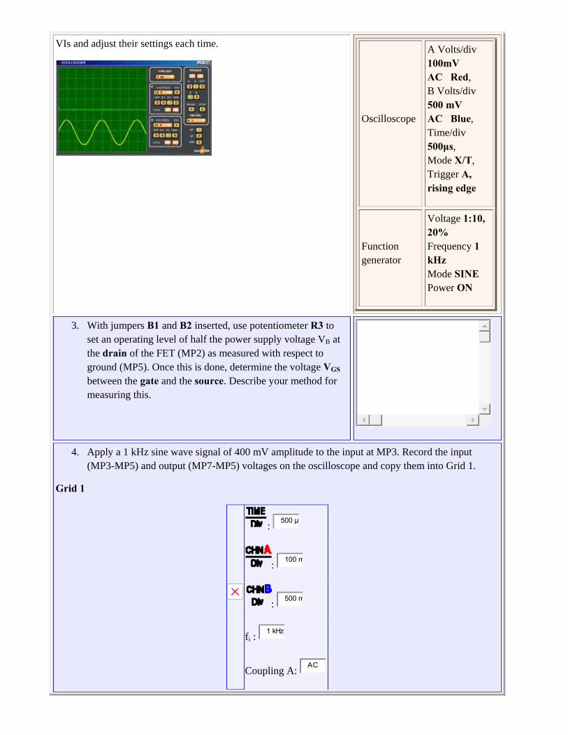
VIs and adjust their settings each time.
Oscilloscope
A Volts/div 100mV AC Red, B Volts/div 500 mV AC Blue, Time/div 500μs, Mode X/T, Trigger A, rising edge
Function generator
Voltage 1:10, 20% Frequency 1 kHz Mode SINE Power ON
3. With jumpers B1 and B2 inserted, use potentiometer R3 to set an operating level of half the power supply voltage VB at the drain of the FET (MP2) as measured with respect to ground (MP5). Once this is done, determine the voltage VGS between the gate and the source. Describe your method for measuring this.
4. Apply a 1 kHz sine wave signal of 400 mV amplitude to the input at MP3. Record the input (MP3-MP5) and output (MP7-MP5) voltages on the oscilloscope and copy them into Grid 1.
Grid 1
: 500 μ
: 100 m
: 500 m
fi : 1 kHz
Coupling A: AC

Coupling B: AC
5. Determine the voltage gain of the circuit Gain vu =
6. Add jumper B4 so that the source is connected to ground via capacitor C4. Apply the same 1 kHz sine wave signal of 400 mV amplitude to the input at MP3. Record the input and output voltages on the oscilloscope and copy them into Grid 2.
Grid 2
: 500 μ
: 100 m
: 500 m
fi : 1 kHz
Coupling A: AC
Coupling B: AC
7. Determine the voltage gain of the circuit with the capacitor at the source. Gain vu =
8. What do you conclude from the results you have obtained?
9. Describe how the circuit operates, highlighting similarities and differences with amplifier circuits using bipolar transistors.
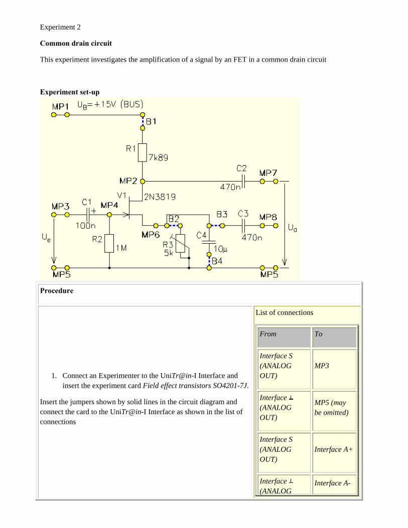
Experiment 2
Common drain circuit
This experiment investigates the amplification of a signal by an FET in a common drain circuit
Experiment set-up
Procedure
1. Connect an Experimenter to the UniTr@in-I Interface and insert the experiment card Field effect transistors SO4201-7J.
Insert the jumpers shown by solid lines in the circuit diagram and connect the card to the UniTr@in-I Interface as shown in the list of connections
List of connections
From To
Interface S (ANALOG OUT)
MP3
Interface (ANALOG OUT)
MP5 (may be omitted)
Interface S (ANALOG OUT)
Interface A+
Interface (ANALOG
Interface A-

OUT)
MP6 (operating point) / MP8 (output)
Interface B+
Interface A- Interface B-
Jumpers
B1, B2, B3
2. Close any virtual instruments you may have open and open the following virtual instruments from the Instruments menu: - Voltmeter B - Function Generator - Oscilloscope (close Voltmeters first) and adjust them as shown in the table.
Since the voltmeters and the oscilloscope cannot be used at the same time, it may be helpful to save one workspace with the voltmeter set up and another with the settings for the oscilloscope. Then you can switch between workspaces instead of having to open and close the VIs and adjust their settings each time.
Settings
Voltmeter B
Range 10V, DC & AV for operating point measurement, AC & Vpp for gain measurement,
Oscilloscope
A Volts/div 500 mV AC Red, B Volts/div 500 mV AC Blue, Time/div 500μs, Mode X/T, Trigger A, rising edge
Function generator
Voltage 1:10, 20% Frequency 1 kHz Mode SINE

Power ON
3. With jumpers B1, B2 and B3 inserted, use potentiometer R3 to set an operating level of half the power supply voltage VB at the drain of the FET (MP2) as measured with respect to ground (MP5). Once this is done, determine the voltage VGS between the gate and the source. Describe your method for measuring this.
4. Apply a 1 kHz sine wave signal of 4 V amplitude to the input at MP3. Record the input (MP3-MP5) and output(MP8-MP5) voltages on the oscilloscope and copy them into Grid 1.
Grid 1
: 500 μ
: 500 m
: 500 m
fi : 1 kHz
Coupling A: AC
Coupling B: AC
5. Determine the voltage gain of the circuit Gain vu =

6. Describe how the circuit operates highlighting similarities and differences with amplifier circuits using bipolar transistors.
7. Summarise the differences between common source and common drain circuits by filling in the following table with the characteristics you have observed during your experiments.
Common source
Common drain
Input resistance re
Output resistance ra
Voltage gain vu
Phase difference j ° °
8. Suggest some applications for the common source and common drain circuits with an FET.
Common source:
Common drain:
