lab 3 revisited - mit opencourseware iap 2008 lecture 4 2 lab 3 revisited ... +2.0v 0.7v 0.4v input...
TRANSCRIPT

6.091 IAP 2008 Lecture 4 1
Lab 3 Revisited
• Zener diodes
R
C

6.091 IAP 2008 Lecture 4 2
Lab 3 Revisited
⎟⎟⎠
⎞⎜⎜⎝
⎛−=
−RCt
sc eVV 1
Vo
V+
V-
.
+
_
+
_
1
2
6
5
5k
5k
5k
3
7
8
4
VCC
Threshold
Control Voltage
Trigger
Output
Discharge
Gnd Reset
CompA
CompB
FlipFlop
Inhibit/Reset
R
S
Q
270
+15
0.1uf
5Kpot
2N2222
0.1uf
1N758
Vin
Vc
Vs = 5 V
• Voltage regulators• 555 timers
Figure by MIT OpenCourseWare.
ready
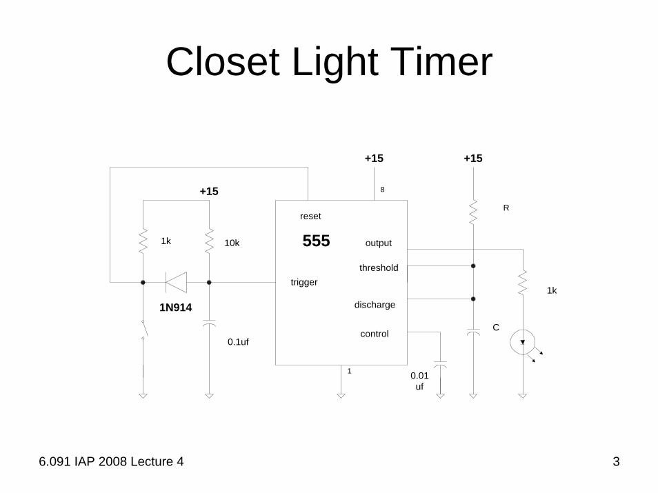
6.091 IAP 2008 Lecture 4 3
Closet Light Timer
+15+15
+15 8
1
reset
trigger
control
threshold
discharge
output10k1k
0.1uf
0.01uf
1k
R
C
555
1N914

6.091 IAP 2008 Lecture 4 4
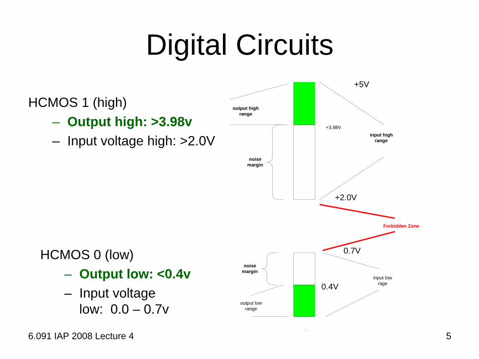
Digital Circuits• Real world analog signals have noise – unavoidable.• Digital circuits offers better noise immunity.• Use voltage to represent “0” and “1”
– Avoid forbidden voltage zone.– Make standards tighter for output than for inputs.
• Data (HCMOS family): 0 (low), 1 (high) – Input voltage low: 0.0 – 0.7v– Input voltage high: >2.0V– Output low: <0.4v– Output high: >3.98v
6.091 IAP 2008 Lecture 4 5.
Digital Circuits
HCMOS 1 (high) – Output high: >3.98v– Input voltage high: >2.0V
output highrange
input highrange
+5V
+3.98V
+2.0V
0.7V
0.4Vinput low
rage
output lowrange
noisemargin
noisemargin
Forbidden Zone
HCMOS 0 (low)– Output low: <0.4v– Input voltage
low: 0.0 – 0.7v

6.091 IAP 2008 Lecture 4 6
Power Requirements• The following power supplies are common for analog
and digital circuits:
+5v for digital circuits, +15v, -15v for analog,-5v, +12v, -12v also used+3.3
• Other voltages generally derived.

6.091 IAP 2008 Lecture 4 7

6.091 IAP 2008 Lecture 4 8
Boolean AlgebraA B = A & B
A = Inverse of A
A B = Inverse of [A&B]
DeMorgan's Law
A B = A + B
A + B = A & B
6.091 IAP 2008 Lecture 4 9
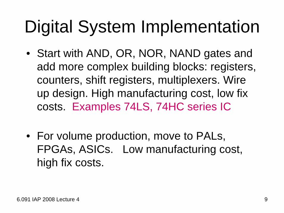
Digital System Implementation• Start with AND, OR, NOR, NAND gates and
add more complex building blocks: registers, counters, shift registers, multiplexers. Wire up design. High manufacturing cost, low fix costs. Examples 74LS, 74HC series IC
• For volume production, move to PALs, FPGAs, ASICs. Low manufacturing cost, high fix costs.

6.091 IAP 2008 Lecture 4 10
Basic Gates
Circle indicates inversion

6.091 IAP 2008 Lecture 4 11
74LS00 NAND Gate
1 2 3 4 5 6 7
A1 B1 Y1 A2 B2 Y2 GND
VCC
Dual-In-Line Package
14 13 12 11 10 9 8
B4 A4 Y4 B3 A3 Y3
This device contains four independent gates eachof which performs the logic NAND function.
Figure by MIT OpenCourseWare, adapted from the National Semiconductor 54LS00 datasheet.

6.091 IAP 2008 Lecture 4 12
74LS02 NOR Gate
Dual-In-Line Package
This device contains four independent gates eachof which performs the logic NOR function.
Figure by MIT OpenCourseWare, adapted from the National Semiconductor 54LS02 datasheet.
1 2 3 4 5 6 7
Y1 A1 B1 Y2 A2 B2 GND
VCC
14 13 12 11 10 9 8
Y4 B4 A4 Y3 B3 A3

6.091 IAP 2008 Lecture 4 13
74LS08 AND Gate
1 2 3 4 5 6 7
A1 B1 Y1 A2 B2 Y2 GND
VCC
Dual-In-Line Package
14 13 12 11 10 9 8
B4 A4 Y4 B3 A3 Y3
This device contains four independent gates eachof which performs the logic AND function.
Figure by MIT OpenCourseWare, adapted from the National Semiconductor 54LS08 datasheet.

6.091 IAP 2008 Lecture 4 14
74LS151 8-1 Multiplexer
ready
1 2 3 4 5 6 7 8
D3 D2 D1 D0 Y W Strobe GND
VCC
16 15 14 13 12 11 10 9
D4 D5 D6 D7 A B C
Data Inputs Outputs
Data Inputs
Dual-in-line Package
Data Select
Select
C B A
X X XL L LL L HL H LL H HH L LH L HH H LH H H
H
SStrobe
LLLLLLLL
LD0D1D2D3D4D5D6D7
H
Y W
D0D1D2D3D4D5D6D7
H = High Level, L = Low Level, X = Don’t Care
D0, D1_D7 = Level of the Respective D Input
InputsOutputs
Figures by MIT OpenCourseWare.

6.091 IAP 2008 Lecture 4 15
Building Logic
• From basic gates, we can build other functions: Exclusive OR Gate
X Y Z0 0 00 1 11 0 11 1 0
XZ
Y
X
Y Z
6.091 IAP 2008 Lecture 4 16
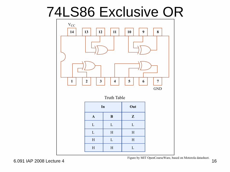
74LS86 Exclusive OR
Figure by MIT OpenCourseWare, based on Motorola datasheet.
In
Truth Table
A
L
L
L
L
H H
H
H
H
H
L L
B Z
Out
1 2 3 4 5 6 7
14 13 12 11 10 9 8
GND
VCC

6.091 IAP 2008 Lecture 4 17
74LS74 D Flip Flop
Q
QSET
CLR
D
CLK
SET-PRESET
CLR
circle indicatesinversion
(active low)
Note both Q and Qbar
Reprinted with permission of National Semiconductor Corporation.
CLK
Q
D

6.091 IAP 2008 Lecture 4 18
Counters
• Ripple carry– Previous stage
used to clock next bit;
• Synchronous– Same clock used
for each bit
B1 B0
0 00 11 01 1
Q
QSET
CLR
D
Q
QSET
CLR
D
Q
QSET
CLR
D
Q
QSET
CLR
D
CLK
CLK
B1
B1
B0
B0
Power connections not shown

6.091 IAP 2008 Lecture 4 19
Building a Synchronous CounterB1 B0 B1 Next0 0 00 1 11 0 11 1 0
• All bits clock on the same clock signal.
• Next count based on current count.
Q
QSET
CLR
D
Q
QSET
CLR
D
CLK
B1B0
B1Next
Power connections not shown

6.091 IAP 2008 Lecture 4 20
Shift Register
Q
QSET
CLR
D
Q
QSET
CLR
D
Q
QSET
CLR
D
Q
QSET
CLR
D
QBQCQDDATA
QA
QB
QC
QD
DATA
CLK
Converts serial data to parallel data or parallel data to serial data.

6.091 IAP 2008 Lecture 4 21
74LS175 4 Bit Shift RegisterClock and Clear are common for all FF. The D FF will store the state of
7 their individual D inputs on the LOW to HIGH Clock transition, causing the individual Q and to follow.
A LOW input on the Clear will force all Q outputs LOW and outputs HIGH independent of Clock or Data inputs.
DSET
Q
CLR Q
DSET
Q
CLR Q
DSET
Q
CLR Q
DSET
Q
CLR Q
74LS175
13 15 12 10 5 4 2
9 1 14 11 6 3clock clear
Q
Q

6.091 IAP 2008 Lecture 4 22
Binary Numbers
• MSB – Most Significant Bit
• LSB – Least Significant Bit
• Let’s build an adder: A+B=S where A,B,S are m bits wide:A: AmAm-1 …A1A0
Dec Binary Hex Dec Binary Hex0 0000 0 8 1000 8
1 0001 1 9 1001 9
2 0010 2 10 1010 A3 0011 3 11 1011 B4 0100 4 12 1100 C5 0101 5 13 1101 D
6 0110 6 14 1110 E7 0111 7 15 1111 F

6.091 IAP 2008 Lecture 4 23
Binary Adder – mth bitCin A B Sum Cout
0 0 0 0 00 0 1 1 00 1 0 1 00 1 1 0 11 0 0 1 01 0 1 0 11 1 0 0 11 1 1 1 1
ADDER
A B
Cin Cout
Sum
Sum =
Cout =
6.091 IAP 2008 Lecture 4 24
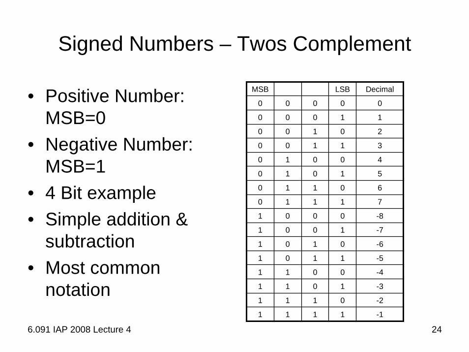
Signed Numbers – Twos Complement
• Positive Number: MSB=0
• Negative Number: MSB=1
• 4 Bit example• Simple addition &
subtraction• Most common
notation
MSB LSB Decimal
0 0 0 0 0
0 0 0 1 1
0 0 1 0 2
0 0 1 1 3
0 1 0 0 4
0 1 0 1 5
0 1 1 0 6
0 1 1 1 7
1 0 0 0 -8
1 0 0 1 -7
1 0 1 0 -6
1 0 1 1 -5
1 1 0 0 -4
1 1 0 1 -3
1 1 1 0 -2
1 1 1 1 -1
6.091 IAP 2008 Lecture 4 25
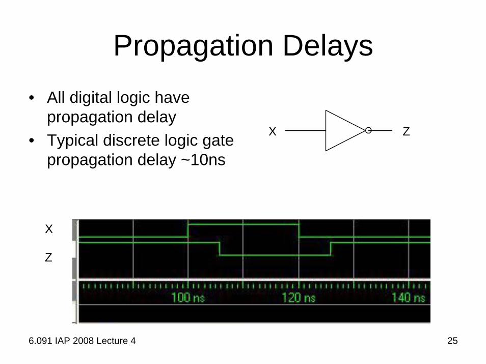
Propagation Delays• All digital logic have
propagation delay• Typical discrete logic gate
propagation delay ~10ns
X Z
Z
X

6.091 IAP 2008 Lecture 4 26
Lab Exercise Ring Oscillator
.
1 110 00

Lab Exercise 4 Bit Counter – Logic Analyzer
1.8432Mhz
crystalosc.
74LS163counter
triangle is symbolfor clock input
6.091 IAP 2008 Lecture 4 27
P
T
LD
CLR
7
10QA
QC
QB
QD
9
1
14
11
12
13
+5
+5
Attach LA probe A2 to QA-QD
Power connections not shown for 74LS163

6.091 IAP 2008 Lecture 4 28
Lab Exercise Ramp Generator
1.8432Mhz
crystalosc.
74LS163counter
triangle is symbolfor clock input
P
T
LD
CLR
7
10QA
QC
QB
QD
9
1
14
11
12
13
+5
+5
4
3
2 2
R
R R R R
2R 2R 2R 2R
Vo
QA
QD
QC
QB
B0
B3
B2
B1
74HC08

6.091 IAP 2008 Lecture 4 29
RAMP Generator Output
6.091 IAP 2008 Lecture 4 30
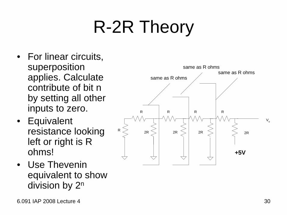
R-2R Theory• For linear circuits,
superposition applies. Calculate contribute of bit n by setting all other inputs to zero.
• Equivalent resistance looking left or right is R ohms!
• Use Thevenin equivalent to show division by 2n
R
R R R R
2R 2R 2R 2R
Vo
+5V
same as R ohmssame as R ohms
same as R ohms

6.091 IAP 2008 Lecture 4 31
DA Summary
• Output from digital to analog conversion are discrete levels.
• More bits means better resolution.• An example of DA conversion
– Current audio CD’s have 16 bit resolution or 65,536 possible output levels
– New DVD audio samples at 192 khz with 24 bit resolution or 224 = 16,777,216
6.091 IAP 2008 Lecture 4 32
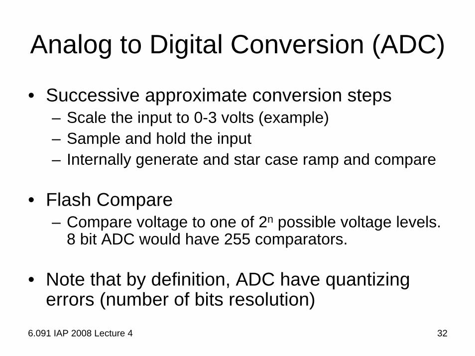
Analog to Digital Conversion (ADC)
• Successive approximate conversion steps– Scale the input to 0-3 volts (example)– Sample and hold the input– Internally generate and star case ramp and compare
• Flash Compare– Compare voltage to one of 2n possible voltage levels.
8 bit ADC would have 255 comparators.
• Note that by definition, ADC have quantizing errors (number of bits resolution)
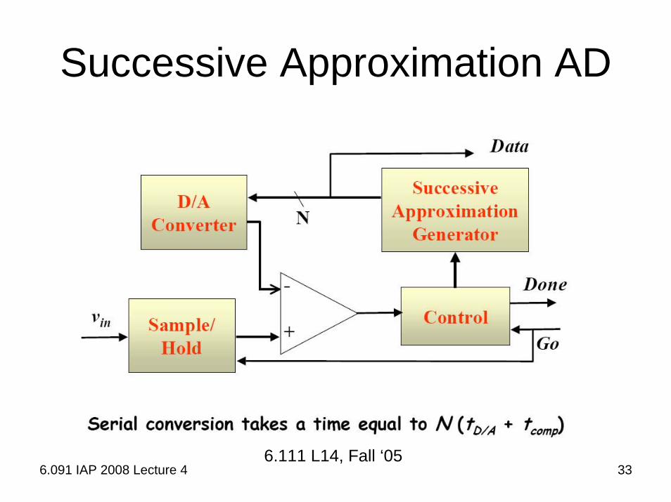
Successive Approximation AD
6.111 L14, Fall ‘056.091 IAP 2008 Lecture 4 33

6.091 IAP 2008 Lecture 4 34
AD7871
Courtesy of Analog Devices. Used with permission.

6.091 IAP 2008 Lecture 4 35
Switch Bounce• All mechanical switches
have “switch bounce”
+5V
Vout

6.091 IAP 2008 Lecture 4 36
Debounce Circuit
+5v
1K
+5v
1K
Q
Qbar
SPDTswitch
T
B
B
T
Q
Qbar
Requires SPDT switch

6.091 IAP 2008 Lecture 4 37
Lab 4
• Use last three aisles on the left at the end of the 6.111 lab
• Pick up IC’s and tools from LA’s.• Return IC’s and tools to LA’s at the
end of the lab

6.091 IAP 2008 Lecture 4 38
Lab 5• Design, build and keep
the electronics for a digital lock.
• Unlock key based on sequence of 0, 1.