lab 2: developing and debugging c programs in mdk-arm …nelsovp/courses...elec 3040/3050 lab manual...
TRANSCRIPT
ELEC 3040/3050 Lab Manual Lab 2 Revised 8/20/14
~ 1 ~
LAB 2: Developing and Debugging C Programs in MDK-ARM for the STM32L100RC Microcontroller
The objective of this laboratory session is to become more familiar with the process for creating, executing and debugging application programs, written in the C language, for the ST Microelectronics ultra-low-power STM32L100RC microcontroller, using the Keil Microcomputer Development Kit for ARM Processors (MDK-ARM). You are to design a C program, containing a “main” program and two subroutines, to exercise various I/O ports and elements of the microcontroller. In the lab, you will also exercise a number of the debug support elements of MDK-ARM, so that you will be better prepared for debugging larger projects later in the semester. An outline of this lab write-up is organized as follows.
A. STM32L100RC microcontroller block diagram and GPIO ports. 1. Block diagram and GPIO ports 2. Configuring the GPIO ports 3. Transferring data to and from GPIO pins
B. Microcontroller Software Setup in C and MDK-ARM C. Data types and variables in C D. Laboratory Exercise E. Lab 2 Deliverables
For reference, the tutorial C Programming for Embedded Systems is available on the course web page, which includes links to additional on-line tutorials. The ARM C Compiler manual is available from the MDK-ARM Help menu, or from the Books pane of your project in the MDK-ARM IDE. A. STM32L100RC General-Purpose Input/Output (GPIO) Pins 1. Microcontroller block diagram and GPIO ports
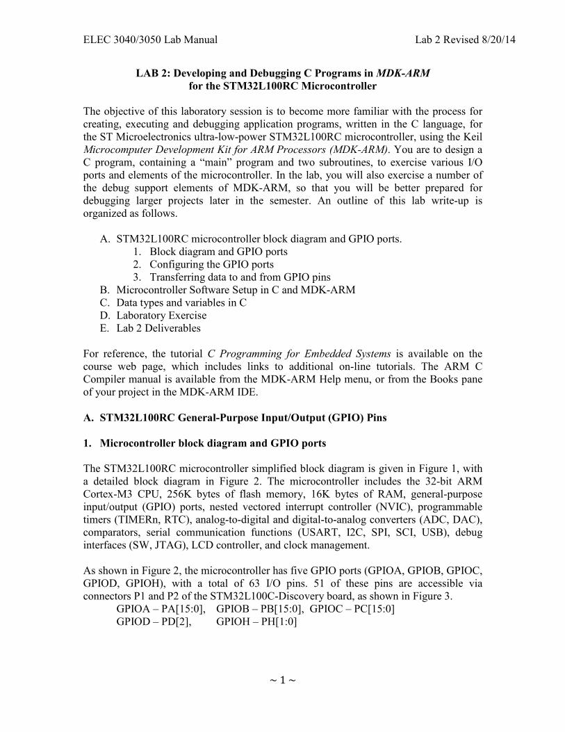
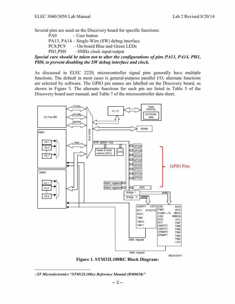
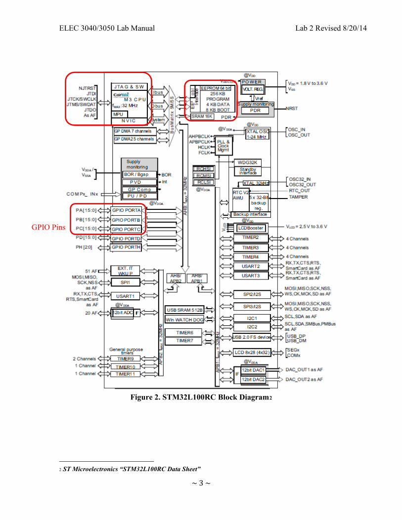
The STM32L100RC microcontroller simplified block diagram is given in Figure 1, with a detailed block diagram in Figure 2. The microcontroller includes the 32-bit ARM Cortex-M3 CPU, 256K bytes of flash memory, 16K bytes of RAM, general-purpose input/output (GPIO) ports, nested vectored interrupt controller (NVIC), programmable timers (TIMERn, RTC), analog-to-digital and digital-to-analog converters (ADC, DAC), comparators, serial communication functions (USART, I2C, SPI, SCI, USB), debug interfaces (SW, JTAG), LCD controller, and clock management. As shown in Figure 2, the microcontroller has five GPIO ports (GPIOA, GPIOB, GPIOC, GPIOD, GPIOH), with a total of 63 I/O pins. 51 of these pins are accessible via connectors P1 and P2 of the STM32L100C-Discovery board, as shown in Figure 3. GPIOA – PA[15:0], GPIOB – PB[15:0], GPIOC – PC[15:0] GPIOD – PD[2], GPIOH – PH[1:0]
ELEC 3040/3050 Lab Manual Lab 2 Revised 8/20/14
~ 2 ~
Several pins are used on the Discovery board for specific functions: PA0 – User button PA13, PA14 – Single-Wire (SW) debug interface PC8,PC9 – On-board Blue and Green LEDs PH1,PH0 – 8MHz clock input/output Special care should be taken not to alter the configurations of pins PA13, PA14, PH1, PH0, to prevent disabling the SW debug interface and clock. As discussed in ELEC 2220, microcontroller signal pins generally have multiple functions. The default in most cases is general-purpose parallel I/O; alternate functions are selected by software. The GPIO pin names are labelled on the Discovery board, as shown in Figure 3. The alternate functions for each pin are listed in Table 5 of the Discovery board user manual, and Table 7 of the microcontroller data sheet.
Figure 1. STM32L100RC Block Diagram1
1 ST Microelectronics “STM32L100xx Reference Manual (RM0038)”
GPIO Pins
ELEC 3040/3050 Lab Manual Lab 2 Revised 8/20/14
~ 3 ~
Figure 2. STM32L100RC Block Diagram2
2 ST Microelectronics “STM32L100RC Data Sheet”
GPIO Pins
ELEC 3040/3050 Lab Manual Lab 2 Revised 8/20/14
~ 4 ~
Figure 3. Top view of the STM32L100C-Discovery Board, showing pin assignments
on 33-pin connectors P1 and P23
3 ST Microelectronics “STM32L100CDiscovery Kit User Manual (UM1656)”
STM32F103C8T6 Microcontroller
ELEC 3040/3050 Lab Manual Lab 2 Revised 8/20/14
~ 5 ~
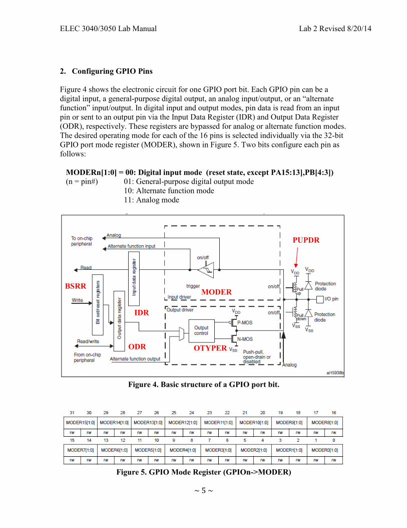
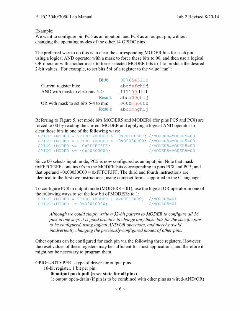
2. Configuring GPIO Pins Figure 4 shows the electronic circuit for one GPIO port bit. Each GPIO pin can be a digital input, a general-purpose digital output, an analog input/output, or an “alternate function” input/output. In digital input and output modes, pin data is read from an input pin or sent to an output pin via the Input Data Register (IDR) and Output Data Register (ODR), respectively. These registers are bypassed for analog or alternate function modes. The desired operating mode for each of the 16 pins is selected individually via the 32-bit GPIO port mode register (MODER), shown in Figure 5. Two bits configure each pin as follows: MODERn[1:0] = 00: Digital input mode (reset state, except PA15:13],PB[4:3]) (n = pin#) 01: General-purpose digital output mode 10: Alternate function mode 11: Analog mode
Figure 4. Basic structure of a GPIO port bit.
Figure 5. GPIO Mode Register (GPIOn->MODER)
OTYPER
PUPDR
ODR
MODER
IDR
BSRR
ELEC 3040/3050 Lab Manual Lab 2 Revised 8/20/14
~ 6 ~
Example: We want to configure pin PC5 as an input pin and PC8 as an output pin, without changing the operating modes of the other 14 GPIOC pins. The preferred way to do this is to clear the corresponding MODER bits for each pin, using a logical AND operator with a mask to force these bits to 00, and then use a logical OR operator with another mask to force selected MODER bits to 1 to produce the desired 2-bit values. For example, to set bits 5:4 of a register to the value “mn”: Bit#: 9876543210 Current register bits: abcdefghij AND with mask to clear bits 5-4: 111100 1111 Result: abcd00ghij OR with mask to set bits 5-4 to mn: 0000mn0000 Result: abcdmnghij Referring to Figure 5, set mode bits MODER5 and MODER8 (for pins PC5 and PC8) are forced to 00 by reading the current MODER and applying a logical AND operator to clear those bits in one of the following ways: GPIOC->MODER = GPIOC->MODER & 0xFFFCF3FF; //MODER8=MODER5=00 GPIOC->MODER = GPIOC->MODER & ~0x00030C00; //MODER8=MODER5=00 GPIOC->MODER &= 0xFFCFF3FF; //MODER8=MODER5=00 GPIOC->MODER &= ~0x00300C00; //MODER8=MODER5=00 Since 00 selects input mode, PC5 is now configured as an input pin. Note that mask 0xFFFCF3FF contains 0’s in the MODER bits corresponding to pins PC8 and PC5, and that operand ~0x00030C00 = 0xFFFCF3FF. The third and fourth instructions are identical to the first two instructions, using compact forms supported in the C language. To configure PC8 in output mode (MODER8 = 01), use the logical OR operator in one of the following ways to set the low bit of MODER8 to 1: GPIOC->MODER = GPIOC->MODER | 0x00010000; //MODER8=01 GPIOC->MODER |= 0x00010000; //MODER8=01
Although we could simply write a 32-bit pattern to MODER to configure all 16 pins in one step, it is good practice to change only those bits for the specific pins to be configured, using logical AND/OR operators, and thereby avoid inadvertently changing the previously-configured modes of other pins.
Other options can be configured for each pin via the following three registers. However, the reset values of these registers may be sufficient for most applications, and therefore it might not be necessary to program them. GPIOn->OTYPER - type of driver for output pins 16-bit register, 1 bit per pin: 0: output push-pull (reset state for all pins) 1: output open-drain (if pin is to be combined with other pins as wired-AND/OR)
ELEC 3040/3050 Lab Manual Lab 2 Revised 8/20/14
~ 7 ~
GPIOn->OSPEEDR – output pin switching speed (lower speeds consume less power) 32-bit register, 2-bits per pin: 00: 400 KHz (reset state for all but PB[3]) 01: 2 MHz, 10: 10MHz, 11: 40MHz GPIOn->PUPDR - activate a pull-up or pull-down resistor on the pin 32-bit register, 2-bits per pin: 00: No pull-up or pull-down (reset state for all but PA[15:13], PB[4]) 01: Pull-up 10: Pull-down 3. Transferring data to and from GPIO pins The states of one or more GPIO pins are determined by reading the 16-bit Input Data Register (IDR) of the GPIO port, and then masking all but the bit(s) of interest. For example, to determine the state of pin PA0: uint16_t bob; //16-bit variable matches IDR size bob = GPIOA->IDR; //read states of all 16 PA[15:0] pins bob &= 0x0001; //mask all but bit 0 to test PA0 if (bob == 0x0001) //do something if PA0=1 Alternatively: if ((GPIOA->IDR & 0x0001) == 0x0001) //do something if PA0=1 A common error is to overlook the fact that reading IDR returns all 16 pin states. For example: if (GPIOA->IDR == 0x0001) //do something if PA0=1 would be true only if all 16 bits of GPIOA match the pattern 0000000000000001. Output pin states are changed by writing to the 16-bit Output Data Register (ODR) of the GPIO port. Note that this changes all pins in that port that are configured as digital general-purpose outputs, but has no effect on pins configured in other modes. GPIOB->ODR = 0x1234; //set PB[15:0] = 0001001000110100 Reading the ODR returns the last value written to it, enabling masks and logical operators (AND, OR, XOR) to change the states of selected pins, without affecting the other pins. GPIOB->ODR &= 0xFFFE; //reset PB0=0 (without changing PB[15:1]) GPIOB->ODR |= 0x0001; //set PB0=1 (without changing PB[15:1]) GPIOB->ODR ^= 0x0001; //complement PB0 state To facilitate changing selected bits, in lieu of using masks and logical operators, each GPIO port has a 32-bit Bit Set/Reset Register (BSSR). Writing 1’s to one or more of the lower 16 bits of BSRR sets those output bits to 1, without affecting the others. Writing 1’s to one or more of the upper 16 bits of BSRR resets those output bits to 0, without affecting the others. Writing 0’s to BSRR has no effect on the corresponding pins. For example, to set and then clear pins PB5 and PB0: GPIOB->BSRR = 0x0021; //set PB5 and PB0 to 1 GPIOB->BSRR = 0x0021 << 16; //reset PB5 and PB0 to 0
ELEC 3040/3050 Lab Manual Lab 2 Revised 8/20/14
~ 8 ~
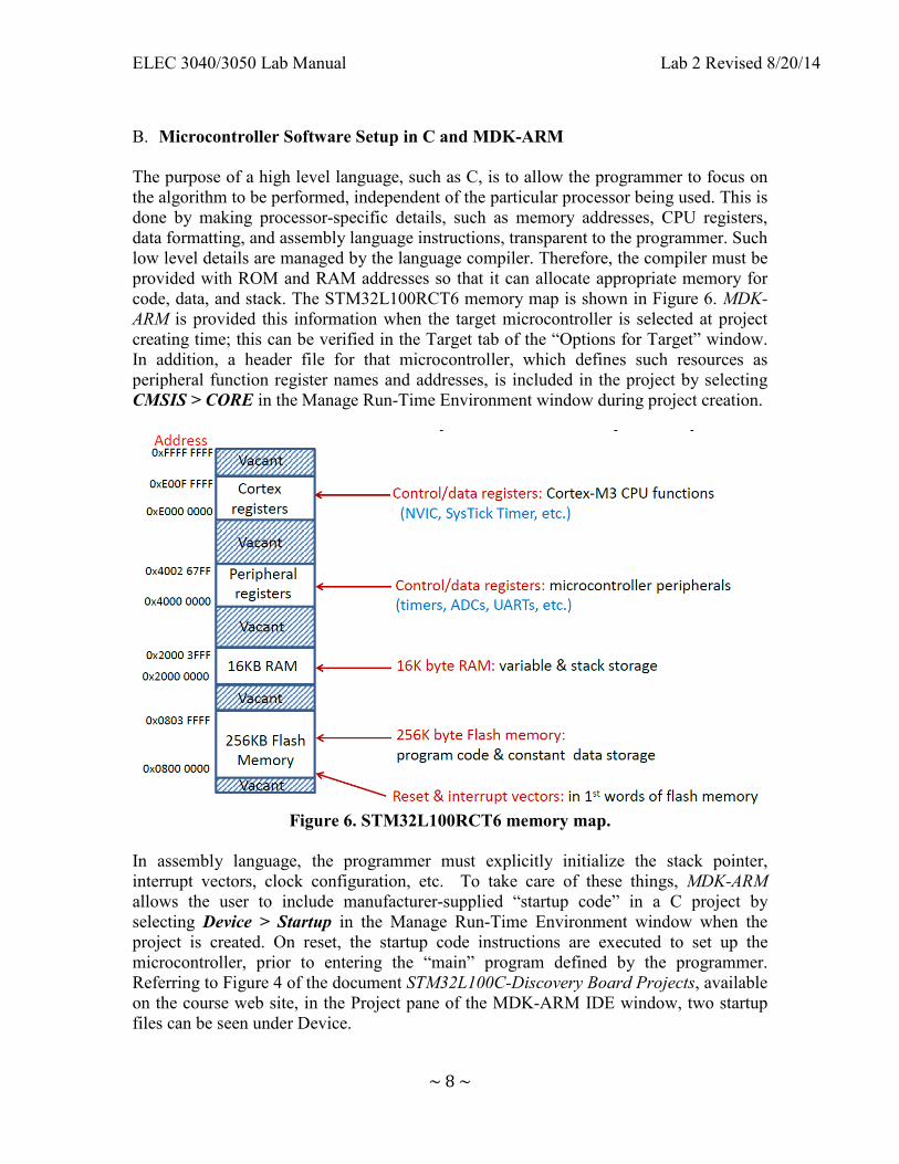
B. Microcontroller Software Setup in C and MDK-ARM The purpose of a high level language, such as C, is to allow the programmer to focus on the algorithm to be performed, independent of the particular processor being used. This is done by making processor-specific details, such as memory addresses, CPU registers, data formatting, and assembly language instructions, transparent to the programmer. Such low level details are managed by the language compiler. Therefore, the compiler must be provided with ROM and RAM addresses so that it can allocate appropriate memory for code, data, and stack. The STM32L100RCT6 memory map is shown in Figure 6. MDK-ARM is provided this information when the target microcontroller is selected at project creating time; this can be verified in the Target tab of the “Options for Target” window. In addition, a header file for that microcontroller, which defines such resources as peripheral function register names and addresses, is included in the project by selecting CMSIS > CORE in the Manage Run-Time Environment window during project creation.
Figure 6. STM32L100RCT6 memory map.
In assembly language, the programmer must explicitly initialize the stack pointer, interrupt vectors, clock configuration, etc. To take care of these things, MDK-ARM allows the user to include manufacturer-supplied “startup code” in a C project by selecting Device > Startup in the Manage Run-Time Environment window when the project is created. On reset, the startup code instructions are executed to set up the microcontroller, prior to entering the “main” program defined by the programmer. Referring to Figure 4 of the document STM32L100C-Discovery Board Projects, available on the course web site, in the Project pane of the MDK-ARM IDE window, two startup files can be seen under Device.
ELEC 3040/3050 Lab Manual Lab 2 Revised 8/20/14
~ 9 ~
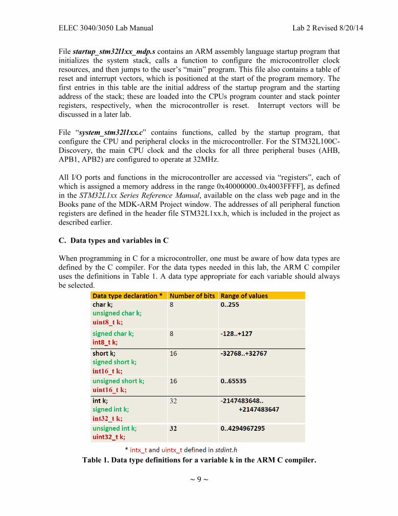
File startup_stm32l1xx_mdp.s contains an ARM assembly language startup program that initializes the system stack, calls a function to configure the microcontroller clock resources, and then jumps to the user’s “main” program. This file also contains a table of reset and interrupt vectors, which is positioned at the start of the program memory. The first entries in this table are the initial address of the startup program and the starting address of the stack; these are loaded into the CPUs program counter and stack pointer registers, respectively, when the microcontroller is reset. Interrupt vectors will be discussed in a later lab. File “system_stm32l1xx.c” contains functions, called by the startup program, that configure the CPU and peripheral clocks in the microcontroller. For the STM32L100C-Discovery, the main CPU clock and the clocks for all three peripheral buses (AHB, APB1, APB2) are configured to operate at 32MHz. All I/O ports and functions in the microcontroller are accessed via “registers”, each of which is assigned a memory address in the range 0x40000000..0x4003FFFF], as defined in the STM32L1xx Series Reference Manual, available on the class web page and in the Books pane of the MDK-ARM Project window. The addresses of all peripheral function registers are defined in the header file STM32L1xx.h, which is included in the project as described earlier. C. Data types and variables in C When programming in C for a microcontroller, one must be aware of how data types are defined by the C compiler. For the data types needed in this lab, the ARM C compiler uses the definitions in Table 1. A data type appropriate for each variable should always be selected.
Table 1. Data type definitions for a variable k in the ARM C compiler.
ELEC 3040/3050 Lab Manual Lab 2 Revised 8/20/14
~ 10 ~
Variables in C can be automatic or static. An automatic variable is declared within a function and is local in scope, i.e. the variable is only accessible within that function. Space for the variable is allocated on the system stack when the function is entered, and then de-allocated when the function is exited. Therefore, values are not retained from one function call to the next. The compiler may choose to allocate CPU registers, instead of memory, for some local variables while in a function, but as with memory, register-based local variable values are not retained between function calls. A static variable can be declared either within or outside of a function. Values of these variables are retained throughout the execution of the program by assigning them to RAM locations that are not reallocated during execution of the program. Any variable defined outside of a function is referred to as global, and has universal scope, i.e. it can be referenced by any function of a program. int count; //global variable void function1 () { count = 1; //function1 writes global variable count } void function2 () { count = count + 1; //function2 modifies global variable count } A static variable can also be defined within a function by inserting the word “static” in front of the variable definition, as in the following character variable declaration. In this case, the variable is local in scope, i.e. accessible only within the defining function. static char bob; Some compilers support volatile variables, whose values can be changed by outside influences, i.e. by factors other than program instructions, such as the value of a timer register or the output of an analog to digital converter. The most common use of volatile variable definitions in embedded systems will be for I/O ports and peripheral function registers. For example, the following defines the addresses of 8-bit I/O ports A and B of a Freescale HCS12 microcontroller.
#define PORTA (*((volatile unsigned char*)(0x0000))) #define PORTB (*((volatile unsigned char*)(0x0001)))
Values read via port A or B are supplied by sources external to the microcontroller, and therefore such ports are declared as data type “volatile unsigned char” at addresses $0000 and $0001, with identifiers PORTA and PORTB, respectively, defined as pointers to these addresses. This allows these identifiers to be used as any other program variable, as illustrated in the following example.. c = PORTB; /* read value from PORTB into variable c */ PORTA = c; /* write value to PORTA from variable c */ The convention for defining peripheral register addresses for ARM microcontrollers is illustrated by the following example, taken from the header file stm32l1xx.h.
ELEC 3040/3050 Lab Manual Lab 2 Revised 8/20/14
~ 11 ~
/*-----------------------------------------------------------------------------------------------------------------------*/ /* Base address of all STM microcontroller peripherals */ #define PERIPH_BASE ((uint32_t)0x40000000) //Peripheral base address #define AHBPERIPH_BASE (PERIPH_BASE + 0x20000) //AHB peripherals /* Base addresses of blocks of GPIO control/data registers */ #define GPIOA_BASE (AHBPERIPH_BASE + 0x0000) //Registers for GPIOA #define GPIOB_BASE (AHBPERIPH_BASE + 0x0400) //Registers for GPIOB /* Address offsets from GPIO base address – block of registers defined as a “structure” */ typedef struct { __IO uint32_t MODER; // GPIO port mode register, Address offset: 0x00 __IO uint16_t OTYPER; // GPIO port output type register, Address offset: 0x04 uint16_t RESERVED0; // Reserved, 0x06 __IO uint32_t OSPEEDR; // GPIO port output speed register, Address offset: 0x08 __IO uint32_t PUPDR; // GPIO port pull-up/pull-down register, Address offset: 0x0C __IO uint16_t IDR; // GPIO port input data register, Address offset: 0x10 uint16_t RESERVED1; // Reserved, 0x12 __IO uint16_t ODR; // GPIO port output data register, Address offset: 0x14 uint16_t RESERVED2; // Reserved, 0x16 __IO uint16_t BSRR; // GPIO port bit set/reset register BSRR, Address offset: 0x18 __IO uint32_t LCKR; // GPIO port configuration lock register, Address offset: 0x1C __IO uint32_t AFR[2]; // GPIO alternate function low register, Address offset: 0x20-0x24 } GPIO_TypeDef; /*-----------------------------------------------------------------------------------------------------------------------*/ The following instruction writes to the output data register of GPIO port B, GPIOB->ODR = 0x1122; The memory address of this register is: 0x40000000 + 0x20000 + 0x0400 + 0x14 = 0x40020414 Peripheral base + AHB peripherals base + GPIOB base + ODR offset The following reads the input data register of GPIO port A and assigns it to variable N. N = GPIOA->IDR; The address of this register is: 0x40000000 + 0x20000 + 0x0000 + 0x10 = 0x40020010 Peripheral base + AHB peripherals base + GPIOA base + IDR offset The programmer should always ensure that the size of the data transferred to and from a register matches the register size and the data type. In the previous examples, 16-bit values are written to/read from the 16-bit ODR and IDR registers.
ELEC 3040/3050 Lab Manual Lab 2 Revised 8/20/14
~ 12 ~
To test or change individual bits of a data value, logical operators (AND, OR, XOR) must be used with a “mask”, as in assembly language. c = GPIOB->IDR & 0x0001; // mask all but bit 0 of data copied to variable c if ((GPIOA->IDR & 0x0001) == 0) // test bit 0 of GPIO port A GPIOA->ODR = c | 0x0001; // write c to GPIO port A, with bit 0 set to 1 Note that there is a difference between bit-parallel operators & (AND) and | (OR), which produce bit-wise results of the corresponding logical operation, and relational operators && (AND) and || (OR), which test and produce TRUE/FALSE results (in C, any non-zero value is considered “TRUE” and a zero value is considered “FALSE”). Consider the difference between the following two statements, where a and b are 32-bit variables: if (a & b) /* test bitwise AND of variables a and b */ if (a && b) /* TRUE only if both a is TRUE and b is TRUE */ if (1) /* non-zero is always TRUE */ if (0) /* zero is always FALSE */ In the first case, the bitwise logical AND of the 32-bit values of a and b is computed, and if all bits = 0, the result would be FALSE, otherwise the result would be TRUE. In the second case, the result is TRUE if variable a is TRUE and if variable b is TRUE. Variables a and b are not combined in the second case. The third case is often used for endless loops – since any non-zero value is always considered TRUE. The fourth case would never be TRUE. D. Pre-lab assignment Each team is to create and debug a C program to meet the following specifications:
1. decade up/down counter: count up or down from 0 to 9, and repeat 2. controlled by two switches, S1 and S2
a. S1: start/stop (1=start, 0 = stop) b. S2: direction (1 = count down, 0 = count up)
3. switch connections on the microcontroller a. S1: I/O port pin PA1 connected to DIO0 on the EEBoard b. S2: I/O port pin PA2 connected to DIO1 on the EEBoard
4. Changing S2 while counting is enabled (S1=1) should change the count direction on the next count change.
5. Display the count value by writing to port pins PC[3:0]. In the laboratory, these lines will be connected to four virtual LEDs.
6. Count period is to be approximately 0.5 s Prior to lab, design the C program with a main program, and two separate ``functions’’ as follows.
• The main program is to initialize port directions and variables, and then execute in an endless loop, calling the delay function, setting the direction variable based on position of switch S2, and calling the counting function if counting is enabled by switch S1.
ELEC 3040/3050 Lab Manual Lab 2 Revised 8/20/14
~ 13 ~
• A delay function is to implement a half-second time delay (“do nothing” for about half a second). If time permits, try to get the delay function to be accurate within 10% of the nominal value (0.5 seconds +/- 10%), or better.
• A counting function is to increment or decrement the count, according to the setting of a direction variable passed as a parameter from main, and display the new value on the LEDs. The count value is to be a static global variable.
In your laboratory notebook, record the following.
1. program flowcharts 2. draft program and functions (or directions to where they are stored on your H:
drive) If program is not in the notebook, be prepared to show the GTA the draft program and functions on your computer at the start of lab.
3. a plan for testing (a test procedure) Teams should be ready to compile their programs and begin testing at the start of the lab period. E. Laboratory exercise Make the following connections between the microcontroller and Digilent EEBoard.
1. The switches are to be push/pull switches, set up for EEBoard digital I/O lines DIO0 and DIO1, and in the Static I/O instrument of Waveforms.
a. S1: DIO0 on the EEBoard b. S2: DIO1 on the EEBoard
2. To display the count value on virtual LEDS, first connect port pins PC[3:0] to EEBoard digital I/O line DIO7-DIO4. Then configure DIO7-DIO4 as LEDS in Waveforms.
Compile and debug the program. In debugging the program, you are expected to demonstrate the use of breakpoints, watch windows, single-step, and other debug features in MDK-ARM. These are described in the document Project Debugging with MDK-ARM, used in the first lab, and available on the course web site. Specifically, do the following in the debugger.
1. Set breakpoints in the main program and in each of the two functions, and verify that the program reaches these breakpoints as expected.
2. While stopped at a breakpoint, record the values of your different program variables (from Watch and/or Call Stack+Locals windows.) Note that the only data values displayed are global variables, and those in the current “scope”, i.e. in the currently-executing function/procedure. So, if you wish to examine a variable in a function F, then you’ll need a breakpoint in F and view the variable in the Call Stack + Locals window.
3. After stopping at a breakpoint, single-step through a few instructions, and record any changes to the variables. Then you may click “run” to continue the program.
4. Using the disassembled program window (upper right), see if you can determine the memory addresses assigned to one of your program variables. Then, in the memory window (bottom right), display the memory area containing that address and verify that the values match those in the variables window.
5. Remove the breakpoints and run the program to verify correct operation.